WO2019116646A1 - 撮像素子および撮像装置 - Google Patents
撮像素子および撮像装置 Download PDFInfo
- Publication number
- WO2019116646A1 WO2019116646A1 PCT/JP2018/032769 JP2018032769W WO2019116646A1 WO 2019116646 A1 WO2019116646 A1 WO 2019116646A1 JP 2018032769 W JP2018032769 W JP 2018032769W WO 2019116646 A1 WO2019116646 A1 WO 2019116646A1
- Authority
- WO
- WIPO (PCT)
- Prior art keywords
- polarization
- type
- members
- types
- polarization member
- Prior art date
- Legal status (The legal status is an assumption and is not a legal conclusion. Google has not performed a legal analysis and makes no representation as to the accuracy of the status listed.)
- Ceased
Links
Images






Classifications
-
- H—ELECTRICITY
- H10—SEMICONDUCTOR DEVICES; ELECTRIC SOLID-STATE DEVICES NOT OTHERWISE PROVIDED FOR
- H10F—INORGANIC SEMICONDUCTOR DEVICES SENSITIVE TO INFRARED RADIATION, LIGHT, ELECTROMAGNETIC RADIATION OF SHORTER WAVELENGTH OR CORPUSCULAR RADIATION
- H10F39/00—Integrated devices, or assemblies of multiple devices, comprising at least one element covered by group H10F30/00, e.g. radiation detectors comprising photodiode arrays
- H10F39/80—Constructional details of image sensors
- H10F39/805—Coatings
- H10F39/8053—Colour filters
-
- H—ELECTRICITY
- H10—SEMICONDUCTOR DEVICES; ELECTRIC SOLID-STATE DEVICES NOT OTHERWISE PROVIDED FOR
- H10F—INORGANIC SEMICONDUCTOR DEVICES SENSITIVE TO INFRARED RADIATION, LIGHT, ELECTROMAGNETIC RADIATION OF SHORTER WAVELENGTH OR CORPUSCULAR RADIATION
- H10F39/00—Integrated devices, or assemblies of multiple devices, comprising at least one element covered by group H10F30/00, e.g. radiation detectors comprising photodiode arrays
- H10F39/80—Constructional details of image sensors
- H10F39/805—Coatings
- H10F39/8057—Optical shielding
-
- G—PHYSICS
- G02—OPTICS
- G02B—OPTICAL ELEMENTS, SYSTEMS OR APPARATUS
- G02B5/00—Optical elements other than lenses
- G02B5/30—Polarising elements
- G02B5/3025—Polarisers, i.e. arrangements capable of producing a definite output polarisation state from an unpolarised input state
- G02B5/3033—Polarisers, i.e. arrangements capable of producing a definite output polarisation state from an unpolarised input state in the form of a thin sheet or foil, e.g. Polaroid
-
- G—PHYSICS
- G02—OPTICS
- G02B—OPTICAL ELEMENTS, SYSTEMS OR APPARATUS
- G02B5/00—Optical elements other than lenses
- G02B5/30—Polarising elements
- G02B5/3025—Polarisers, i.e. arrangements capable of producing a definite output polarisation state from an unpolarised input state
- G02B5/3058—Polarisers, i.e. arrangements capable of producing a definite output polarisation state from an unpolarised input state comprising electrically conductive elements, e.g. wire grids, conductive particles
-
- H—ELECTRICITY
- H04—ELECTRIC COMMUNICATION TECHNIQUE
- H04N—PICTORIAL COMMUNICATION, e.g. TELEVISION
- H04N25/00—Circuitry of solid-state image sensors [SSIS]; Control thereof
- H04N25/70—SSIS architectures; Circuits associated therewith
-
- H—ELECTRICITY
- H10—SEMICONDUCTOR DEVICES; ELECTRIC SOLID-STATE DEVICES NOT OTHERWISE PROVIDED FOR
- H10F—INORGANIC SEMICONDUCTOR DEVICES SENSITIVE TO INFRARED RADIATION, LIGHT, ELECTROMAGNETIC RADIATION OF SHORTER WAVELENGTH OR CORPUSCULAR RADIATION
- H10F39/00—Integrated devices, or assemblies of multiple devices, comprising at least one element covered by group H10F30/00, e.g. radiation detectors comprising photodiode arrays
- H10F39/80—Constructional details of image sensors
- H10F39/806—Optical elements or arrangements associated with the image sensors
Definitions
- the present technology relates to an imaging device.
- the present invention relates to an imaging device and an imaging device including a polarizer.
- an imaging device capable of acquiring polarization information is known. By utilizing polarization information, the contrast of the image can be improved or unnecessary information can be deleted.
- an imaging device for acquiring such polarization information for example, an imaging device provided with a polarization member using a wire grid has been proposed (for example, see Patent Document 1).
- polarization information is acquired by providing a plurality of types of polarization members having different polarization angles on the photoelectric conversion element incident light side.
- polarization members having different internal structures are combined.
- the present technology is produced in view of such a situation, and it is an object of the present technology to improve the accuracy of polarization information obtained in an imaging device including a polarizer.
- the present technology has been made to solve the above-mentioned problems, and the first side surface of the present technology arranges a plurality of types of polarization members formed by rotating or symmetrically moving polarization members having the same internal structure.
- It is an imaging device provided with an image sensor which comprises a light polarizer, a photoelectric conversion element which changes into a charge the light which entered via each of a plurality of kinds of polarization members, and the image sensor. This brings about the effect of making the characteristics of the polarization pixel uniform by using a plurality of types of polarization members obtained by rotating or symmetrically moving the polarization members having the same internal structure.
- At least one of the plurality of types of polarization members may be formed by at least symmetrically moving another type of polarization member. This brings about the effect
- the plurality of types of polarization members are the first type of polarization members and the second type of polarization members rotated 90 degrees clockwise with the left and right of the first type of polarization members reversed. And the third type of polarization member in which the first type of polarization member is rotated 90 degrees counterclockwise, and the fourth type of polarization member in which the first type of polarization member is horizontally reversed. Good.
- the polarization angle of the first type polarization member may be in the range of 5 degrees to 40 degrees.
- the plurality of types of polarization members are a first type of polarization member, and a second type of polarization member obtained by rotating the first type of polarization member by 45 degrees counterclockwise.
- a third type of polarization member obtained by rotating the first type of polarization member by 90 degrees counterclockwise and a fourth type of polarization member obtained by rotating the first type of polarization member by 135 degrees counterclockwise May be
- the shape of the area of the plurality of types of polarizing members may be a regular octagon or a circle.
- the first side surface may further include a light shielding film disposed in an area outside the plurality of types of polarizing members. This brings about the effect
- the first side surface may further include a lens disposed so as to be inscribed on the incident side of the plurality of types of polarizing members. This brings about the effect
- the plurality of types of polarization members are a first type of polarization member, and a second type of polarization member obtained by rotating the first type of polarization member by 60 degrees counterclockwise.
- the first type of polarizing member may be provided with a third type of polarizing member rotated 120 degrees counterclockwise.
- the shape of the area of the plurality of types of polarizing members may be a regular hexagon.
- the plurality of types of polarization members are a first type of polarization member and a second type of polarization member rotated 120 degrees clockwise with the left and right of the first type of polarization member reversed.
- a third type of polarization member obtained by rotating the first type of polarization member by 60 degrees counterclockwise, and a fourth type of polarization obtained by horizontally reversing the first type of polarization member and rotated 60 degrees clockwise
- each of the plurality of types of polarizers may be arranged such that the shapes of the regions of the plurality of types of polarizing members overlap due to parallel movement.
- the shape of the area of the plurality of types of polarization members is n ⁇ m square (n and m are integers) It may be.
- the plurality of types of polarization members have a parallelogram shape and a wire grid type having a plurality of line-shaped conductive light shielding material layers parallel to one side of the parallelogram It may be a polarization member.
- the plurality of linear conductive light shielding material layers in the plurality of types of polarizing members be parallel to the long side of the parallelogram.
- the plurality of types of polarizing members may have a parallelogram shape in which the length of each side is equal, and the inner angle may be a combination of 60 degrees and 120 degrees.
- the plurality of types of polarization members are at least three types of polarization members.
- an imaging device including a polarizer in an imaging device including a polarizer, it is possible to achieve an excellent effect that the accuracy of polarization information to be obtained can be improved.
- the effect described here is not necessarily limited, and may be any effect described in the present disclosure.
- FIG. 1 is a diagram illustrating an example of an entire configuration of an imaging device according to an embodiment of the present technology. It is a figure showing an example of a sectional view of image sensor 11 in an embodiment of this art. It is a top view showing an example of arrangement of light polarizer 14 in a 1st embodiment of this art. It is a figure which shows the example of a relation of the polarization direction of light polarizer 14 and a sine function in a 1st embodiment of this art. It is a top view showing an example of arrangement of light polarizer 14 in a 2nd embodiment of this art. It is a top view which shows the other example of arrangement
- Imaging device First embodiment (example of four kinds of polarizing members by rotational movement and symmetrical movement) 3. Second embodiment (example of four types of polarization members by rotational movement) 4. Third embodiment (example in which the shape of the area of the polarizing member is a regular octagon) 5. Fourth embodiment (example in which the shape of the area of the polarizing member is circular) 6. Fifth embodiment (example of three types of polarization members by rotational movement) 7. Sixth embodiment (example of six kinds of polarizing members by rotational movement and symmetrical movement) 8. Seventh Embodiment (an example in which the shape of the region of the polarizing member is a parallelogram)
- FIG. 1 is a diagram illustrating an example of an entire configuration of an imaging device according to an embodiment of the present technology.
- This imaging device comprises a pixel area 10 and a peripheral circuit unit.
- the peripheral circuit unit includes a vertical drive circuit 20, a horizontal drive circuit 30, a control circuit 40, a column signal processing circuit 50, and an output circuit 60.
- the pixel area 10 is a pixel array in which a plurality of imaging elements 11 including photoelectric conversion units are arranged in a two-dimensional array.
- the imaging device 11 includes, for example, a photodiode serving as a photoelectric conversion unit and a plurality of pixel transistors.
- the vertical drive circuit 20 drives the imaging element 11 in units of rows.
- the vertical drive circuit 20 is configured of, for example, a shift register.
- the vertical drive circuit 20 selects a pixel drive wiring, and supplies a pulse for driving the imaging element 11 to the selected pixel drive wiring.
- the vertical drive circuit 20 selectively scans the respective imaging elements 11 of the pixel area 10 sequentially in the vertical direction in row units, and based on the signal charges generated in the photoelectric conversion units of the respective imaging elements 11 according to the light reception amount.
- the pixel signal is supplied to the column signal processing circuit 50 via the vertical signal line 19.
- the horizontal drive circuit 30 drives the column signal processing circuit 50 in units of columns.
- the horizontal drive circuit 30 is configured of, for example, a shift register.
- the horizontal drive circuit 30 sequentially selects each of the column signal processing circuits 50 by sequentially outputting horizontal scanning pulses, and pixel signals from each of the column signal processing circuits 50 are transmitted via the horizontal signal line 59.
- the output circuit 60 is made to output.
- the control circuit 40 controls the entire imaging device.
- the control circuit 40 receives an input clock and data instructing an operation mode and the like, and outputs data such as internal information of the imaging device. That is, the control circuit 40 generates clock signals and control signals that become the reference of operations of the vertical drive circuit 20, the column signal processing circuit 50, the horizontal drive circuit 30, etc. based on the vertical synchronization signal, horizontal synchronization signal and master clock. Generate Then, these signals are input to the vertical drive circuit 20, the column signal processing circuit 50, the horizontal drive circuit 30, and the like.
- the column signal processing circuit 50 is disposed, for example, for each column of the imaging elements 11, and performs signal processing such as noise removal for each pixel column on signals output from the imaging elements 11 for one row. That is, the column signal processing circuit 50 performs signal processing such as CDS (Correlated Double Sampling) for removing fixed pattern noise unique to the imaging device 11, signal amplification, AD (Analog to Digital) conversion, and the like.
- a horizontal selection switch (not shown) is connected between the output stage of the column signal processing circuit 50 and the horizontal signal line 59.
- the output circuit 60 performs signal processing on signals sequentially supplied from each of the column signal processing circuits 50 through the horizontal signal line 59 and outputs the processed signals. At this time, the output circuit 60 buffers the signal from the column signal processing circuit 50.
- the output circuit 60 may perform black level adjustment, column variation correction, various digital signal processing, and the like on the signal from the column signal processing circuit 50.
- FIG. 2 is a diagram illustrating an example of a cross-sectional view of the imaging element 11 according to the embodiment of the present technology.
- the imaging device 11 has a structure in which the lens 12, the color filter 13, the polarizer 14, the wiring layer 15, and the substrate 17 are sequentially stacked from the incident light side.
- this structure is merely an example, and for example, it may be a backside illumination type structure in which light is irradiated from a surface different from that of the wiring layer 15.
- the lens 12 is a condensing element provided for each imaging element 11. Incident light is collected by the lens 12 and taken into the imaging device 11.
- the color filter 13 is a filter that passes a specific wavelength range. For example, a filter that passes red, blue, green, etc. is assumed. However, this color filter 13 is provided as needed, and can be omitted when acquiring only polarization information.
- the polarizer 14 is an element for acquiring polarization information.
- the polarization member used as the polarizer 14 is, for example, a wire grid type having a plurality of linear conductive light shielding material layers. The light passing through the polarizer 14 is incident on the substrate 17 through the wiring layer 15.
- the substrate 17 is a substrate on which the circuit of the imaging device 11 is formed.
- the photoelectric conversion element 16 is formed on the substrate 17.
- the photoelectric conversion element 16 is an element that converts incident light into charge, and for example, a photodiode is used.
- the wiring layer 15 is a region in which a metal layer which is a wiring between circuits formed on the substrate 17 is formed.
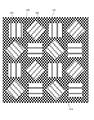
- FIG. 3 is a top view showing an arrangement example of the polarizers 14 in the first embodiment of the present technology.
- a rectangular square polarization member having the same internal structure is used to rotationally or symmetrically move (invert) the polarization member to form four types of polarization members.
- the internal structure of the polarization member is determined by the length, pitch, etc. of the linear conductive light shielding material layer (wire grid).
- the angle of the wire grid is the polarization angle. In this case, the length of the wire grid does not change even if it is rotationally moved or symmetrically moved.
- the internal structure of the polarization member is the same, even if it is rotated or moved symmetrically, only the polarization angle changes, and the characteristics as the polarization member (for example, transmission axis transmittance, reflection axis transmittance, extinction ratio Etc.) is not considered.
- the first type polarization member 111 the second type polarization member 112
- the third type polarization member 113 the fourth type polarization member 114
- the polarization members 111 to 114 all have the same internal structure.
- these polarization members 111 to 114 are arranged so as to overlap by translational movement.
- characters are attached so that the angle can be easily understood visually, but this is merely a mark for describing rotational movement and symmetrical movement. In fact, these letters are not engraved.
- the second type of polarizing member 112 is obtained by horizontally inverting the first type of polarizing member 111 and rotating it 90 degrees clockwise.
- the third type of polarization member 113 is obtained by rotating the first type of polarization member 111 by 90 degrees counterclockwise.
- the fourth type of polarization member 114 is formed by horizontally reversing the first type of polarization member 111.
- these polarization members 111 to 114 are formed by rotationally moving or symmetrically moving polarization members having the same internal structure.
- at least one type of polarization members (in this example, the second type polarization member 112 and the fourth type polarization member 114) are other types of polarization members (in this example, the first type)
- the polarization member 111) is formed by at least a symmetrical movement.
- FIG. 4 is a diagram showing an example of the relationship between the polarization direction of the polarizer 14 and the sine function in the first embodiment of the present technology.
- the polarization angles of the four types of polarization members 111 to 114 be ⁇ 1 to ⁇ 4 . These four polarization angles ⁇ 1 to ⁇ 4 are plotted in the horizontal axis direction, and the corresponding pixel output values are plotted in the vertical direction, and fitting is performed on a sine function (or cosine function). As a result, it is possible to obtain polarization information (degree of polarization and polarization angle) of incident light by finding the angle ⁇ when the pixel output value indicates the maximum value Imax. Thus, to obtain polarization information, at least three polarizer angles are required to perform fitting to a sine function or the like. Therefore, although polarization information can be obtained by four types of pixels as in this example, polarization information can not be correctly obtained by, for example, two types of pixels.
- the polarization angle theta 1 of the first type of polarization member 111 approaches 0 degrees or 45 degrees, the polarization angle of the two pixels are substantially the same, thus resulting in longer obtained only two pixels . Therefore, the polarization angle theta 1 of the first type of polarization member 111, as shown below, it is assumed that in the range of 5 degrees to 40 degrees. 5 ⁇ ⁇ 1 ⁇ 40 At this time, the polarization angle theta 1 is more desirably 22.5 degrees of the center value.
- the transmission axis transmittance, the reflection axis transmittance, and the extinction ratio of the plurality of types of polarization members are all equal in principle. This improves the accuracy of the maximum value, the minimum value, and the angle at which the maximum value is obtained of the sine function derived from a plurality of types of pixel outputs. Therefore, it is possible to improve the accuracy of the degree of polarization of light obtained by computing them, the azimuth angle of the object normal, the zenith angle, and the distance information and shape information of the object calculated based on them.
- FIG. 5 is a top view showing an arrangement example of the polarizers 14 in the second embodiment of the present technology.
- the polarization member is rotationally moved to form four types of polarization members 121 to 124 by using a square polarization member having the same internal structure.
- the second type of polarization member 122 is obtained by rotating the first type of polarization member 121 by 45 degrees counterclockwise.
- the third type of polarization member 123 is obtained by rotating the first type of polarization member 121 counterclockwise by 90 degrees.
- the fourth type of polarization member 124 is obtained by rotating the first type of polarization member 121 by 135 degrees counterclockwise. This makes it possible to form four types of pixels in which polarizing members having the same transmittance but different angles are disposed.
- FIG. 6 is a top view showing another arrangement example of the polarizer 14 in the second embodiment of the present technology.
- the lens 125 is disposed on the upper surface of each of the polarization members 121 to 124.
- the lens 125 corresponds to the lens 12 shown in the above cross-sectional view.
- the polarizing members 121 to 124 be disposed so as to be inscribed in the lens 125.
- the lenses 125 are disposed so as to be inscribed on the incident side of the polarization members 121 to 124, and the condensed light can be efficiently incident on the polarization members 121 to 124.
- the characteristics as the polarization member are matched by using four types of polarization members in which the square member having the same internal structure is rotationally moved. Polarization information with high accuracy.
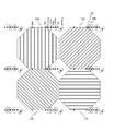
- FIG. 7 is a top view showing an arrangement example of the polarizers 14 in the third embodiment of the present technology.
- the polarization members are rotationally moved to form four types of polarization members 131 to 134. These polarization members 131 to 134 are arranged to overlap by translation.
- the aperture ratio of the imaging device can be increased by making the shape of the polarization member a regular octagon.
- the second type of polarization member 132 is formed by rotating the first type of polarization member 131 counterclockwise by 45 degrees.
- the third type of polarization member 133 is formed by rotating the first type of polarization member 131 counterclockwise by 90 degrees.
- the fourth type of polarization member 134 is formed by rotating the first type of polarization member 131 counterclockwise by 135 degrees. This makes it possible to form four types of pixels in which polarizing members having the same transmittance but different angles are disposed.
- the third embodiment when there is a gap between the polarization members 131 to 134, it is desirable to dispose the light shielding film 139 outside the polarization members 131 to 134. Thereby, it is possible to prevent the light from entering the light other than the polarization members 131 to 134.
- Drawing 8 is a figure showing an example of arrangement layout of light polarizer 14 in a 3rd embodiment of this art.
- the transistor 136 and the contact 137 on the substrate 17 are shown.
- the arrangement of transistors and the arrangement of wirings are translationally symmetrical.
- the shape of the area of each polarizing member can be made translationally symmetrical by making the shape of the area of the polarizing member regular octagon. This makes it possible to equalize the optical properties other than the polarization angles of the four pixels.
- FIG. 9 is a top view showing another arrangement example of the polarizer 14 in the third embodiment of the present technology.
- the lens 135 is disposed on the upper surface of each of the polarization members 131 to 134.
- the lens 135 corresponds to the lens 12 shown in the above-described cross-sectional view.
- the lenses 135 are disposed so as to be inscribed on the incident side of the polarization members 131 to 134, and the condensed light can be efficiently incident on the polarization members 131 to 134.
- the characteristics as the polarization member are matched by using four types of polarization members in which the regular octagonal polarization members having the same internal structure are rotationally moved. Polarization information with high accuracy.
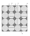
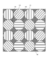
- FIG. 10 is a top view showing an arrangement example of the polarizers 14 in the fourth embodiment of the present technology.
- circular polarization members having the same internal structure are used to rotationally move the polarization members to form four types of polarization members 141 to 144.
- the second type of polarization member 142 is formed by rotating the first type of polarization member 141 counterclockwise by 45 degrees.
- the third type of polarization member 143 is obtained by rotating the first type of polarization member 141 counterclockwise by 90 degrees.
- the fourth type of polarization member 144 is formed by rotating the first type of polarization member 141 counterclockwise by 135 degrees.
- the characteristics as the polarization member are made to match by using four types of polarization members in which the circular polarization members having the same internal structure are rotationally moved. Polarization information with high accuracy can be obtained.
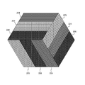
- FIG. 11 is a top view showing an exemplary arrangement of polarizers 14 according to the fifth embodiment of the present technology.
- the polarization member is rotationally moved to form three types of polarization members 151 to 153 by using a regular hexagonal polarization member having the same internal structure. As described above, polarization information can be obtained with polarization members of three different angles.
- the second type of polarization member 152 is obtained by rotating the first type of polarization member 151 counterclockwise by 60 degrees.
- the third type of polarization member 153 is formed by rotating the first type of polarization member 151 counterclockwise by 120 degrees.
- the shape of the area of the second type of polarization member 152 and the area of the third type of polarization member 153 is the same as the shape of the area of the first type of polarization member 151.
- the imaging elements are arranged in a honeycomb arrangement, and no gap can be formed between the polarization members 151 to 153.
- the characteristics as a polarizing member are matched by using three types of polarizing members in which the regular hexagonal polarizing members having the same internal structure are rotationally moved. Polarization information with high accuracy.
- FIG. 12 is a top view showing an arrangement example of the polarizer 14 in the sixth embodiment of the present technology.
- the polarization member is rotationally moved or symmetrically moved (reversed movement) using a regular hexagonal polarization member having the same internal structure to form six kinds of polarization members 161 to 166. .
- the second type of polarization member 162 is formed by rotating the first type of polarization member 161 horizontally and rotating it clockwise by 120 degrees.
- the third type of polarization member 163 is formed by rotating the first type of polarization member 161 counterclockwise by 60 degrees.
- the fourth type of polarization member 164 is obtained by inverting the first type of polarization member 161 horizontally and rotating it clockwise by 60 degrees.
- the fifth type of polarization member 165 is obtained by rotating the first type of polarization member 161 counterclockwise by 120 degrees.
- the sixth type of polarization member 166 is formed by reversing the left and right of the first type of polarization member 161.
- the polarization angle theta 1 of the first type of polarization member 161 approaches 0 ° or 30 °, the polarization angles of the two types of pixels become substantially the same, and as a result, only three types of pixels can be obtained. . Therefore, the polarization angle theta 1 of the first type of polarization member 161, as shown below, it is assumed that in the range of 5 degrees to 25 degrees. 5 ⁇ ⁇ 1 ⁇ 25 At this time, the polarization angle theta 1 is more desirably 15 degrees of the median.
- FIG. 13 is a top view showing a first arrangement example of the polarizer 14 in the seventh embodiment of the present technology.
- three types of polarization members 211 to 213 are formed by rotating the polarization members using parallelogram polarization members having the same internal structure.
- a line-shaped conductive light shielding material layer (wire grid) is formed in parallel to any one side of the parallelogram.
- the second type of polarization member 212 is obtained by rotating the first type of polarization member 211 counterclockwise by 60 degrees.
- the third type of polarization member 213 is obtained by rotating the first type of polarization member 211 clockwise by 60 degrees.
- each side of the parallelogram is equal and has a rhombus shape.
- the internal angle is a combination of 60 degrees and 120 degrees.
- FIG. 14 is a top view showing a second arrangement example of the polarizer 14 in the seventh embodiment of the present technology.
- the polarization member is rotationally moved using a parallelogram polarization member having the same internal structure. Form two types of polarization members 221-223. The manner of rotational movement is also the same as in the first arrangement example described above.
- adjacent sides of the parallelogram have different lengths. Thus, when placed, gaps may occur. In that case, it is desirable to dispose a light shielding film on the outside of the polarizing members 221 to 223. Thereby, it is possible to prevent the light from entering the light other than the polarization members 221 to 223.
- the wire grid is formed parallel to any one side of the parallelogram, but in this second arrangement example, the wire grid is a parallelogram It is desirable to be parallel to the long side.
- FIG. 16 is a top view showing a third arrangement example of the polarizer 14 in the seventh embodiment of the present technology.
- four types of polarization members 231 to 234 are formed by rotating the polarization members using parallelogram polarization members having the same internal structure. .
- the second type of polarization member 232 is obtained by horizontally inverting the first type of polarization member 231 and rotating it 90 degrees clockwise.
- the third type of polarization member 233 is obtained by rotating the first type of polarization member 231 counterclockwise by 90 degrees.
- the fourth type of polarization member 234 is formed by reversing the left and right of the first type of polarization member 231.
- adjacent sides of the parallelogram may have different lengths.
- a gap may be generated between the polarization members 231 to 234, it is desirable to dispose a light shielding film outside the polarization members 231 to 234 as in the second arrangement example described above.
- the wire grid is parallel to the longer side of the parallelogram, as in the second arrangement example described above.
- the present technology can also be configured as follows.
- a polarizer having a plurality of types of polarization members disposed by rotating or symmetrically moving polarization members having the same internal structure;
- An image pickup device comprising: a photoelectric conversion element that converts light incident through each of the plurality of types of polarization members into an electric charge.
- the plurality of types of polarization members are a first type of polarization member, a second type of polarization member in which the first type of polarization member is horizontally turned 90 degrees clockwise, and the first type of polarization member In the above (1) or (2), provided with a third type of polarization member obtained by rotating the polarization member of the present invention by 90 degrees counterclockwise and a fourth type of polarization member obtained by reversing the first type of polarization member left and right Image sensor.
- a polarization angle of the first type of polarization member is in a range of 5 degrees to 40 degrees.
- the plurality of types of polarization members are a first type of polarization member, a second type of polarization member in which the first type of polarization member is rotated 45 degrees counterclockwise, and the first type of polarization member
- the imaging according to (1) further including: a third type of polarization member rotated 90 degrees counterclockwise, and a fourth type of polarization member rotated 135 degrees counterclockwise of the first type polarization member element.
- the imaging device according to (5), wherein the shape of the region of the plurality of types of polarization members is a regular octagon.
- the imaging device according to (5), wherein the shape of the region of the plurality of types of polarization members is circular.
- the image pickup device further including a light shielding film disposed in an area outside the plurality of types of polarizing members.
- the plurality of types of polarization members are a first type of polarization member, a second type of polarization member obtained by rotating the first type of polarization member by 60 degrees counterclockwise, and the first type of polarization member
- the imaging device according to (1) or (2), further including: a third type of polarization member rotated counterclockwise by 120 degrees.
- the imaging device wherein the shape of the region of the plurality of types of polarization members is a regular hexagon.
- the plurality of types of polarization members are a first type of polarization member, a second type of polarization member in which the first type of polarization member is horizontally reversed and rotated clockwise by 120 degrees, and the first type of polarization member A third type of polarization member rotated counterclockwise by 60 degrees, a fourth type polarization member rotated leftwardly by 60 degrees clockwise, and the first type of polarization member;
- a fifth type of polarization member obtained by rotating a type of polarization member by 120 degrees counterclockwise and a sixth type of polarization member obtained by inverting the first type of polarization member left and right The imaging device of description.
- the imaging device according to (1) or (2), wherein the plurality of types of polarizers are arranged such that the shapes of the regions of the plurality of types of polarization members overlap due to parallel movement.
- the shape of the region of the plurality of types of polarizing members is n ⁇ m square (where n and m are integers); The imaging device of description.
- the plurality of types of polarization members described above are wire grid type polarization members having a shape of a parallelogram, and having a plurality of line-shaped conductive light shielding material layers parallel to one side of the parallelogram The imaging element as described in (1).
- a polarizer in which a plurality of types of polarization members are disposed by rotating or symmetrically moving polarization members having the same internal structure, and light incident through each of the plurality of types of polarization members is converted into charge
- An imaging device in which a plurality of imaging devices including a photoelectric conversion device are arranged.
- Reference Signs List 10 10 pixel area 11 imaging device 12 lens 13 color filter 14 polarizer 15 wiring layer 16 photoelectric conversion device 17 substrate 19 vertical signal line 20 vertical drive circuit 30 horizontal drive circuit 40 control circuit 50 column signal processing circuit 59 horizontal signal line 60 output circuit 111 to 114, 121 to 124, 131 to 134, 141 to 144, 151 to 153, 161 to 166, 211 to 213, 221 to 223, 231 to 234 Polarizing members 125, 135 Lenses 129, 139, 149 Light shielding film 136 transistor 137 contacts
Landscapes
- Physics & Mathematics (AREA)
- General Physics & Mathematics (AREA)
- Optics & Photonics (AREA)
- Engineering & Computer Science (AREA)
- Multimedia (AREA)
- Signal Processing (AREA)
- Polarising Elements (AREA)
- Solid State Image Pick-Up Elements (AREA)
- Optical Filters (AREA)
Abstract
偏光子を備える撮像素子において、得られる偏光情報の精度を向上させる。 撮像素子は、入射光側から、偏光子および光電変換素子を備える。偏光子は、複数種類の偏光部材を配置したものである。複数種類の偏光部材は、内部構造が同一の偏光部材であり、それを回転移動または対称移動させることにより複数種類の偏光部材として形成される。光電変換素子は、複数種類の偏光部材のそれぞれを介して入射した光を電荷に変換するものである。
Description
本技術は、撮像素子に関する。詳しくは、偏光子を備える撮像素子および撮像装置に関する。
従来、偏光情報を取得することを可能とする撮像装置が知られている。偏光情報を利用することにより、画像のコントラストを改善し、または、不要な情報を削除することができる。このような偏光情報を取得する撮像装置として、例えば、ワイヤーグリッドを利用した偏光部材を備える撮像装置が提案されている(例えば、特許文献1参照。)。
上述の従来技術では、光電変換素子入射光側に、偏光角度の異なる複数種類の偏光部材を設けて偏光情報を取得している。しかしながら、従来技術においては、偏光部材の内部構造が異なるものを組み合わせるため、偏光画素の特性に差が生じ、得られる偏光情報の精度が悪化するおそれがある。
本技術はこのような状況に鑑みて生み出されたものであり、偏光子を備える撮像素子において、得られる偏光情報の精度を向上させることを目的とする。
本技術は、上述の問題点を解消するためになされたものであり、その第1の側面は、内部構造が同一の偏光部材を回転移動または対称移動させてなる複数種類の偏光部材を配置した偏光子と、上記複数種類の偏光部材のそれぞれを介して入射した光を電荷に変換する光電変換素子とを具備する撮像素子およびその撮像素子を備える撮像装置である。これにより、内部構造が同一の偏光部材を回転移動または対称移動させてなる複数種類の偏光部材を使用することにより、偏光画素の特性を均一化させるという作用をもたらす。
また、この第1の側面において、上記複数種類の偏光部材の少なくとも何れか一種類の偏光部材は、他の種類の偏光部材を少なくとも対称移動させてなるものであってもよい。これにより、偏光画素の特性の均一化を容易にするという作用をもたらす。
また、この第1の側面において、上記複数種類の偏光部材は、第1種類の偏光部材と、上記第1種類の偏光部材を左右反転して時計回りに90度回転した第2種類の偏光部材と、上記第1種類の偏光部材を反時計回りに90度回転した第3種類の偏光部材と、上記第1種類の偏光部材を左右反転した第4種類の偏光部材とを備えるようにしてもよい。このとき、上記第1種類の偏光部材の偏光角度は、5度から40度の範囲内であってもよい。
また、この第1の側面において、上記複数種類の偏光部材は、第1種類の偏光部材と、上記第1種類の偏光部材を反時計回りに45度回転した第2種類の偏光部材と、上記第1種類の偏光部材を反時計回りに90度回転した第3種類の偏光部材と、上記第1種類の偏光部材を反時計回りに135度回転した第4種類の偏光部材とを備えるようにしてもよい。この場合において、上記複数種類の偏光部材の領域の形状は、正八角形または円形であってもよい。
また、この第1の側面において、上記複数種類の偏光部材の外側の領域に配置された遮光膜をさらに具備してもよい。これにより、偏光部材以外への光の入射を防ぐという作用をもたらす。
また、この第1の側面において、上記複数種類の偏光部材の入射側においてそれぞれ内接するように配置されたレンズをさらに具備してもよい。これにより、集光された光を効率良く偏光部材に入射させるという作用をもたらす。
また、この第1の側面において、上記複数種類の偏光部材は、第1種類の偏光部材と、上記第1種類の偏光部材を反時計回りに60度回転した第2種類の偏光部材と、上記第1種類の偏光部材を反時計回りに120度回転した第3種類の偏光部材とを備えるようにしてもよい。この場合において、上記複数種類の偏光部材の領域の形状は、正六角形であってもよい。
また、この第1の側面において、上記複数種類の偏光部材は、第1種類の偏光部材と、上記第1種類の偏光部材を左右反転して時計回りに120度回転した第2種類の偏光部材と、上記第1種類の偏光部材を反時計回りに60度回転した第3種類の偏光部材と、上記第1種類の偏光部材を左右反転して時計回りに60度回転した第4種類の偏光部材と、上記第1種類の偏光部材を反時計回りに120度回転した第5種類の偏光部材と、上記第1種類の偏光部材を左右反転した第6種類の偏光部材とを備えるようにしてもよい。
また、この第1の側面において、上記偏光子は、上記複数種類の偏光部材の領域の形状が平行移動によって重なるように上記複数種類のそれぞれを配置したものであってもよい。
また、この第1の側面において、上記複数種類の偏光部材における回転移動の角度がn種類であるとき、上記複数種類の偏光部材の領域の形状はn×m角形(nおよびmは整数)であってもよい。
また、この第1の側面において、上記複数種類の偏光部材は、平行四辺形の形状を有し、その平行四辺形の一辺に平行である複数のライン状の導電遮光材料層を有するワイヤーグリッドタイプの偏光部材であってもよい。この場合において、上記複数種類の偏光部材における上記複数のライン状の導電遮光材料層は、平行四辺形の長い辺に平行であることが望ましい。また、上記複数種類の偏光部材は、各辺の長さが等しい平行四辺形の形状を有し、その内角の角度を60度と120度の組合せとしてもよい。また、上記複数種類の偏光部材は、少なくとも3種類の偏光部材である。
本技術によれば、偏光子を備える撮像素子において、得られる偏光情報の精度を向上させることができるという優れた効果を奏し得る。なお、ここに記載された効果は必ずしも限定されるものではなく、本開示中に記載されたいずれかの効果であってもよい。
以下、本技術を実施するための形態(以下、実施の形態と称する)について説明する。説明は以下の順序により行う。
1.撮像装置
2.第1の実施の形態(回転移動および対称移動による4種類の偏光部材の例)
3.第2の実施の形態(回転移動による4種類の偏光部材の例)
4.第3の実施の形態(偏光部材の領域の形状を正八角形とした例)
5.第4の実施の形態(偏光部材の領域の形状を円形とした例)
6.第5の実施の形態(回転移動による3種類の偏光部材の例)
7.第6の実施の形態(回転移動および対称移動による6種類の偏光部材の例)
8.第7の実施の形態(偏光部材の領域の形状を平行四辺形とした例)
1.撮像装置
2.第1の実施の形態(回転移動および対称移動による4種類の偏光部材の例)
3.第2の実施の形態(回転移動による4種類の偏光部材の例)
4.第3の実施の形態(偏光部材の領域の形状を正八角形とした例)
5.第4の実施の形態(偏光部材の領域の形状を円形とした例)
6.第5の実施の形態(回転移動による3種類の偏光部材の例)
7.第6の実施の形態(回転移動および対称移動による6種類の偏光部材の例)
8.第7の実施の形態(偏光部材の領域の形状を平行四辺形とした例)
<1.撮像装置>
[撮像装置の全体構成]
図1は、本技術の実施の形態における撮像装置の全体構成の一例を示す図である。この撮像装置は、画素領域10および周辺回路部からなる。周辺回路部は、垂直駆動回路20と、水平駆動回路30と、制御回路40と、カラム信号処理回路50と、出力回路60とを備える。
[撮像装置の全体構成]
図1は、本技術の実施の形態における撮像装置の全体構成の一例を示す図である。この撮像装置は、画素領域10および周辺回路部からなる。周辺回路部は、垂直駆動回路20と、水平駆動回路30と、制御回路40と、カラム信号処理回路50と、出力回路60とを備える。
画素領域10は、光電変換部を含む複数の撮像素子11を、2次元アレイ状に配列した画素アレイである。この撮像素子11は、光電変換部となる例えばフォトダイオードと、複数の画素トランジスタを含む。
垂直駆動回路20は、行単位で撮像素子11を駆動するものである。この垂直駆動回路20は、例えばシフトレジスタによって構成される。この垂直駆動回路20は、画素駆動配線を選択して、その選択された画素駆動配線に撮像素子11を駆動するためのパルスを供給する。これにより、垂直駆動回路20は、画素領域10の各撮像素子11を行単位で順次垂直方向に選択走査し、各撮像素子11の光電変換部において受光量に応じて生成された信号電荷に基づく画素信号を、垂直信号線19を介して、カラム信号処理回路50に供給する。
水平駆動回路30は、列単位にカラム信号処理回路50を駆動するものである。この水平駆動回路30は、例えばシフトレジスタによって構成される。この水平駆動回路30は、水平走査パルスを順次出力することによって、カラム信号処理回路50の各々を順番に選択し、カラム信号処理回路50の各々から画素信号を、水平信号線59を介して、出力回路60に出力させる。
制御回路40は、撮像装置の全体を制御するものである。この制御回路40は、入力クロックと、動作モードなどを指令するデータとを受け取り、撮像装置の内部情報などのデータを出力する。すなわち、この制御回路40は、垂直同期信号、水平同期信号およびマスタクロックに基いて、垂直駆動回路20、カラム信号処理回路50および水平駆動回路30などの動作の基準となるクロック信号や制御信号を生成する。そして、これらの信号を垂直駆動回路20、カラム信号処理回路50および水平駆動回路30等に入力する。
カラム信号処理回路50は、撮像素子11の例えば列ごとに配置され、1行分の撮像素子11から出力される信号に対し、画素列ごとにノイズ除去などの信号処理を行うものである。すなわち、このカラム信号処理回路50は、撮像素子11固有の固定パターンノイズを除去するためのCDS(Correlated Double Sampling)や、信号増幅、AD(Analog to Digital)変換等の信号処理を行う。カラム信号処理回路50の出力段には、図示しない水平選択スイッチが水平信号線59との間に接続される。
出力回路60は、カラム信号処理回路50の各々から水平信号線59を通して順次に供給される信号に対し、信号処理を行って出力するものである。その際、この出力回路60は、カラム信号処理回路50からの信号をバッファリングする。また、この出力回路60は、カラム信号処理回路50からの信号に対して、黒レベル調整、列ばらつき補正、各種デジタル信号処理などを行うようにしてもよい。
[撮像素子の構成]
図2は、本技術の実施の形態における撮像素子11の断面図の一例を示す図である。
図2は、本技術の実施の形態における撮像素子11の断面図の一例を示す図である。
この例では、撮像素子11は、入射光側から、レンズ12、カラーフィルタ13、偏光子14、配線層15、基板17の順に重ねた構造を想定する。ただし、この構造は一例に過ぎず、例えば、配線層15とは異なる面から光を照射させる裏面照射型の構造であってもよい。
レンズ12は、撮像素子11毎に設けられる集光素子である。入射光は、このレンズ12によって集光されて撮像素子11内に取り込まれる。
カラーフィルタ13は、特定の波長域を通過させるフィルタである。例えば、赤、青、緑などを通過させるフィルタが想定される。ただし、このカラーフィルタ13は、必要に応じて設けられるものであり、偏光情報のみを取得する場合には省くことができる。
偏光子14は、偏光情報を取得するための素子である。この偏光子14として用いられる偏光部材は、例えば複数のライン状の導電遮光材料層を有するワイヤーグリッドタイプのものが用いられる。この偏光子14を通過した光は、配線層15を介して基板17に入射する。
基板17は、撮像素子11の回路が形成される基板である。この基板17には、光電変換素子16が形成される。この光電変換素子16は、入射した光を電荷に変換する素子であり、例えばフォトダイオードが用いられる。
配線層15は、基板17に形成された回路間の配線であるメタル層が形成される領域である。
<2.第1の実施の形態>
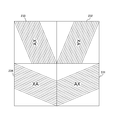
図3は、本技術の第1の実施の形態における偏光子14の配置例を示す上面図である。
図3は、本技術の第1の実施の形態における偏光子14の配置例を示す上面図である。
この第1の実施の形態では、内部構造が同一の正四角形の偏光部材を用いて、その偏光部材を回転移動または対称移動(反転移動)させて4つの種類の偏光部材を形成する。ワイヤーグリッドタイプの偏光部材を想定すると、偏光部材の内部構造は、ライン状の導電遮光材料層(ワイヤーグリッド)の長さやピッチなどにより決定される。ワイヤーグリッドの角度が偏光角度となる。この場合、ワイヤーグリッドの長さは、回転移動または対称移動させても変わらない。すなわち、偏光部材の内部構造が同一であれば、回転移動または対称移動させても、偏光角度が変わるだけであり、偏光部材としての特性(例えば、透過軸透過率、反射軸透過率、消光比など)には影響しないと考えられる。
この例では、第1種類の偏光部材111、第2種類の偏光部材112、第3種類の偏光部材113、第4種類の偏光部材114の4つの種類の偏光部材を示している。偏光部材111乃至114は、全て同一の内部構造を有している。また、これらの偏光部材111乃至114は、平行移動によって重なるように配置される。なお、この実施の形態および以降の一部の実施の形態においては、角度を視覚的に容易に理解できるよう文字を付しているが、これはあくまでも回転移動および対称移動を説明するための目印であり、実際にこれらの文字が刻印されているわけでない。
第1種類の偏光部材111を基準とすると、第2種類の偏光部材112は、第1種類の偏光部材111を左右反転して、それを時計回りに90度回転したものとなっている。また、第3種類の偏光部材113は、第1種類の偏光部材111を反時計回りに90度回転したものとなっている。また、第4種類の偏光部材114は、第1種類の偏光部材111を左右反転したものとなっている。
すなわち、これら偏光部材111乃至114は、内部構造が同一の偏光部材を回転移動または対称移動させて形成されたものである。また、その中の少なくとも何れか一種類の偏光部材(この例では、第2種類の偏光部材112および第4種類の偏光部材114)は、他の種類の偏光部材(この例では、第1種類の偏光部材111)を少なくとも対称移動させて形成されたものである。
図4は、本技術の第1の実施の形態における偏光子14の偏光方向と正弦関数との関係例を示す図である。
4種類の偏光部材111乃至114のそれぞれの偏光角度をθ1乃至θ4とする。これら4種類の偏光角度θ1乃至θ4を横軸方向にプロットし、対応する画素出力値を縦方向にプロットして、正弦関数(または余弦関数)に対してフィッティングを行う。その結果、画素出力値が最大値Imaxを示すときの角度φを求めることにより、入射光の偏光情報(偏光度や偏光角)を得ることができる。このように、偏光情報を得るために、正弦関数等に対するフィッティングを行うため、最低3種類の偏光子角度が必要である。したがって、この例のように4種類の画素では偏光情報が得られるが、例えば2種類の画素では偏光情報を正しく得ることができない。
この第1の実施の形態においては、4種類の偏光部材111乃至114の偏光角度θ1乃至θ4は、
θ2=90-θ1
θ3=90+θ1
θ4=180-θ1
の関係を有している。
θ2=90-θ1
θ3=90+θ1
θ4=180-θ1
の関係を有している。
ただし、第1種類の偏光部材111の偏光角度θ1が0度や45度に近づくと、2種類の画素の偏光角度が略同じになり、結果的に2種類の画素しか得られなくなってしまう。そこで、第1種類の偏光部材111の偏光角度θ1は、以下に示すように、5度から40度の範囲内にあることを想定する。
5≦θ1≦40
このとき、偏光角度θ1は、中央値の22.5度であることがより望ましい。
5≦θ1≦40
このとき、偏光角度θ1は、中央値の22.5度であることがより望ましい。
このように、本技術の第1の実施の形態によれば、内部構造が同一の正四角形の偏光部材を回転移動または対称移動させた4つの種類の偏光部材を用いることにより、偏光部材としての特性を一致させ、精度の高い偏光情報を得ることができる。すなわち、角度が異なる複数種類の偏光部材を配した撮像素子において、複数種類の偏光部材の透過軸透過率、反射軸透過率、消光比が全て原理的に等しくなる。これにより、複数種類の画素出力から導出される正弦関数の最大値、最小値、および、最大値が得られる角度の精度が向上する。したがって、それらを演算することにより得られる光の偏光度や、物体法線の方位角、天頂角、それらに基づいて計算される物体の距離情報や形状情報の正確性を向上させることができる。
<3.第2の実施の形態>
図5は、本技術の第2の実施の形態における偏光子14の配置例を示す上面図である。
図5は、本技術の第2の実施の形態における偏光子14の配置例を示す上面図である。
この第2の実施の形態では、内部構造が同一の正四角形の偏光部材を用いて、その偏光部材を回転移動させて4つの種類の偏光部材121乃至124を形成する。
第1種類の偏光部材121を基準とすると、第2種類の偏光部材122は、第1種類の偏光部材121を反時計回りに45度回転したものとなっている。また、第3種類の偏光部材123は、第1種類の偏光部材121を反時計回りに90度回転したものとなっている。また、第4種類の偏光部材124は、第1種類の偏光部材121を反時計回りに135度回転したものとなっている。これにより、透過率が等しく角度のみが異なる偏光部材を配した4種類の画素を形成することができる。
この第2の実施の形態のように、偏光部材121乃至124の間に隙間ができる場合には、偏光部材121乃至124の外側に遮光膜129を配置することが望ましい。これにより、偏光部材121乃至124以外への光の入射を防ぐことができる。
図6は、本技術の第2の実施の形態における偏光子14の他の配置例を示す上面図である。
この例では、偏光部材121乃至124のそれぞれの上面にレンズ125を配置している。このレンズ125は、上述の断面図に示したレンズ12に相当するものである。レンズ125が設けられている場合、偏光部材121乃至124は、レンズ125に内接するように配置することが望ましい。これにより、レンズ125が偏光部材121乃至124の入射側においてそれぞれ内接するように配置され、集光された光を効率よく偏光部材121乃至124に入射させることができる。
このように、本技術の第2の実施の形態によれば、内部構造が同一の正四角形の偏光部材を回転移動させた4つの種類の偏光部材を用いることにより、偏光部材としての特性を一致させ、精度の高い偏光情報を得ることができる。
<4.第3の実施の形態>
図7は、本技術の第3の実施の形態における偏光子14の配置例を示す上面図である。
図7は、本技術の第3の実施の形態における偏光子14の配置例を示す上面図である。
この第3の実施の形態では、内部構造が同一の正八角形の偏光部材を用いて、その偏光部材を回転移動させて4つの種類の偏光部材131乃至134を形成する。これらの偏光部材131乃至134は、平行移動によって重なるように配置される。特に、この第3の実施の形態では、偏光部材の形状を正八角形とすることにより、撮像素子の開口率を高くすることができる。
第1種類の偏光部材131を基準とすると、第2種類の偏光部材132は、第1種類の偏光部材131を反時計回りに45度回転したものとなっている。また、第3種類の偏光部材133は、第1種類の偏光部材131を反時計回りに90度回転したものとなっている。また、第4種類の偏光部材134は、第1種類の偏光部材131を反時計回りに135度回転したものとなっている。これにより、透過率が等しく角度のみが異なる偏光部材を配した4種類の画素を形成することができる。
この第3の実施の形態のように、偏光部材131乃至134の間に隙間ができる場合には、偏光部材131乃至134の外側に遮光膜139を配置することが望ましい。これにより、偏光部材131乃至134以外への光の入射を防ぐことができる。
図8は、本技術の第3の実施の形態における偏光子14の配置レイアウトの一例を示す図である。
この例では、偏光部材131乃至134に加えて、基板17上のトランジスタ136やコンタクト137を示している。ここに示したように、一般的に画素レイアウトはトランジスタの配置や配線の配置が並進対称である。この第3の実施の形態では、偏光部材の領域の形状を正八角形にすることにより、個々の偏光部材の領域の形状を並進対称にすることができる。これにより、4つの画素の偏光角度以外の光学的性質を等しくすることができる。
図9は、本技術の第3の実施の形態における偏光子14の他の配置例を示す上面図である。
この例では、偏光部材131乃至134のそれぞれの上面にレンズ135を配置している。このレンズ135は、上述の断面図に示したレンズ12に相当するものである。レンズ135が設けられている場合、レンズ135は、偏光部材131乃至134に内接するように配置することが望ましい。これにより、レンズ135が偏光部材131乃至134の入射側においてそれぞれ内接するように配置され、集光された光を効率良く偏光部材131乃至134に入射させることができる。
このように、本技術の第3の実施の形態によれば、内部構造が同一の正八角形の偏光部材を回転移動させた4つの種類の偏光部材を用いることにより、偏光部材としての特性を一致させ、精度の高い偏光情報を得ることができる。
<5.第4の実施の形態>
図10は、本技術の第4の実施の形態における偏光子14の配置例を示す上面図である。
図10は、本技術の第4の実施の形態における偏光子14の配置例を示す上面図である。
この第4の実施の形態では、内部構造が同一の円形の偏光部材を用いて、その偏光部材を回転移動させて4つの種類の偏光部材141乃至144を形成する。
第1種類の偏光部材141を基準とすると、第2種類の偏光部材142は、第1種類の偏光部材141を反時計回りに45度回転したものとなっている。また、第3種類の偏光部材143は、第1種類の偏光部材141を反時計回りに90度回転したものとなっている。また、第4種類の偏光部材144は、第1種類の偏光部材141を反時計回りに135度回転したものとなっている。これにより、透過率が等しく、各画素の偏光角度以外の光学的性質を等しい偏光部材を配した4種類の画素を形成することができる。
この第4の実施の形態のように、偏光部材141乃至144の間に隙間ができる場合には、偏光部材141乃至144の外側に遮光膜149を配置することが望ましい。これにより、偏光部材141乃至144以外への光の入射を防ぐことができる。
このように、本技術の第4の実施の形態によれば、内部構造が同一の円形の偏光部材を回転移動させた4つの種類の偏光部材を用いることにより、偏光部材としての特性を一致させ、精度の高い偏光情報を得ることができる。
<6.第5の実施の形態>
図11は、本技術の第5の実施の形態における偏光子14の配置例を示す上面図である。
図11は、本技術の第5の実施の形態における偏光子14の配置例を示す上面図である。
この第5の実施の形態では、内部構造が同一の正六角形の偏光部材を用いて、その偏光部材を回転移動させて3つの種類の偏光部材151乃至153を形成する。上述のように、異なる3種類の角度の偏光部材があれば偏光情報を取得することができる。
第1種類の偏光部材151を基準とすると、第2種類の偏光部材152は、第1種類の偏光部材151を反時計回りに60度回転したものとなっている。また、第3種類の偏光部材153は、第1種類の偏光部材151を反時計回りに120度回転したものとなっている。なお、第2種類の偏光部材152と第3種類の偏光部材153の領域の形状は、第1種類の偏光部材151の領域の形状と同一になる。
この第5の実施の形態では、撮像素子をハニカム配列により配置しており、偏光部材151乃至153の間に隙間はできないようになっている。
このように、本技術の第5の実施の形態によれば、内部構造が同一の正六角形の偏光部材を回転移動させた3つの種類の偏光部材を用いることにより、偏光部材としての特性を一致させ、精度の高い偏光情報を得ることができる。
<7.第6の実施の形態>
図12は、本技術の第6の実施の形態における偏光子14の配置例を示す上面図である。
図12は、本技術の第6の実施の形態における偏光子14の配置例を示す上面図である。
この第6の実施の形態では、内部構造が同一の正六角形の偏光部材を用いて、その偏光部材を回転移動または対称移動(反転移動)させて6つの種類の偏光部材161乃至166を形成する。
第1種類の偏光部材161を基準とすると、第2種類の偏光部材162は、第1種類の偏光部材161を左右反転して、それを時計回りに120度回転したものとなっている。また、第3種類の偏光部材163は、第1種類の偏光部材161を反時計回りに60度回転したものとなっている。また、第4種類の偏光部材164は、第1種類の偏光部材161を左右反転して、それを時計回りに60度回転したものとなっている。また、第5種類の偏光部材165は、第1種類の偏光部材161を反時計回りに120度回転したものとなっている。また、第6種類の偏光部材166は、第1種類の偏光部材161を左右反転したものとなっている。
この第1の実施の形態においては、6種類の偏光部材161乃至166の偏光角度θ1乃至θ6は、
θ2=60-θ1
θ3=60+θ1
θ4=120-θ1
θ5=120+θ1
θ6=180-θ1
の関係を有している。
θ2=60-θ1
θ3=60+θ1
θ4=120-θ1
θ5=120+θ1
θ6=180-θ1
の関係を有している。
ただし、第1種類の偏光部材161の偏光角度θ1が0度や30度に近づくと、2種類の画素の偏光角度が略同じになり、結果的に3種類の画素しか得られなくなってしまう。そこで、第1種類の偏光部材161の偏光角度θ1は、以下に示すように、5度から25度の範囲内にあることを想定する。
5≦θ1≦25
このとき、偏光角度θ1は、中央値の15度であることがより望ましい。
5≦θ1≦25
このとき、偏光角度θ1は、中央値の15度であることがより望ましい。
このように、本技術の第6の実施の形態によれば、内部構造が同一の正六角形の偏光部材を回転移動または対称移動させた6つの種類の偏光部材を用いることにより、偏光部材としての特性を一致させ、精度の高い偏光情報を得ることができる。
<8.第7の実施の形態>
図13は、本技術の第7の実施の形態における偏光子14の第1の配置例を示す上面図である。
図13は、本技術の第7の実施の形態における偏光子14の第1の配置例を示す上面図である。
この第7の実施の形態の第1の配置例では、内部構造が同一の平行四辺形の偏光部材を用いて、その偏光部材を回転移動させて3つの種類の偏光部材211乃至213を形成する。ワイヤーグリッドタイプの偏光部材を想定すると、この第7の実施の形態では、ライン状の導電遮光材料層(ワイヤーグリッド)が平行四辺形の何れか一辺に平行に形成される。
第1種類の偏光部材211を基準とすると、第2種類の偏光部材212は、第1種類の偏光部材211を反時計回りに60度回転したものとなっている。また、第3種類の偏光部材213は、第1種類の偏光部材211を時計回りに60度回転したものとなっている。
この第1の配置例においては、平行四辺形の各辺は等しく、菱形の形状を有する。また、内角の角度は、60度と120度の組合せとなる。これにより、3つの種類の偏光部材211乃至213を密に配置することができ、3つの種類の偏光部材211乃至213の間に隙間が生じない。
図14は、本技術の第7の実施の形態における偏光子14の第2の配置例を示す上面図である。
この第7の実施の形態の第2の配置例では、上述の第1の配置例と同様に、内部構造が同一の平行四辺形の偏光部材を用いて、その偏光部材を回転移動させて3つの種類の偏光部材221乃至223を形成する。回転移動の態様についても上述の第1の配置例と同様である。
この第2の配置例においては、平行四辺形の隣り合う辺は異なる長さを有する。したがって、配置した際には隙間が生じ得る。その場合には、偏光部材221乃至223の外側には遮光膜を配置することが望ましい。これにより、偏光部材221乃至223以外への光の入射を防ぐことができる。
なお、カラーの撮像素子を用いる場合、偏光部材221乃至223と平行に異なるカラーの撮像素子を配置することが望ましい。これにより、上述の隙間を無くすことができる。例えば、図15に示すように、青色画素224、緑色画素225および赤色画素226の撮像素子を配置することが想定される。
また、上述のようにこの第7の実施の形態では、ワイヤーグリッドが平行四辺形の何れか一辺に平行に形成されるが、この第2の配置例においては、ワイヤーグリッドが平行四辺形のより長い辺に平行であることが望ましい。
図16は、本技術の第7の実施の形態における偏光子14の第3の配置例を示す上面図である。
この第7の実施の形態の第3の配置例では、内部構造が同一の平行四辺形の偏光部材を用いて、その偏光部材を回転移動させて4つの種類の偏光部材231乃至234を形成する。
第1種類の偏光部材231を基準とすると、第2種類の偏光部材232は、第1種類の偏光部材231を左右反転して、それを時計回りに90度回転したものとなっている。また、第3種類の偏光部材233は、第1種類の偏光部材231を反時計回りに90度回転したものとなっている。また、第4種類の偏光部材234は、第1種類の偏光部材231を左右反転したものとなっている。
この第3の配置例においては、平行四辺形の隣り合う辺は異なる長さを有してもよい。その場合には、偏光部材231乃至234の間には隙間が生じ得るが、上述の第2の配置例と同様に、偏光部材231乃至234の外側には遮光膜を配置することが望ましい。
また、この第3の配置例においては、上述の第2の配置例と同様に、ワイヤーグリッドが平行四辺形のより長い辺に平行であることが望ましい。
このように、本技術の第7の実施の形態によれば、内部構造が同一の平行四辺形の偏光部材を回転移動させた少なくとも3つの種類の偏光部材を用いることにより、偏光部材としての特性を一致させ、精度の高い偏光情報を得ることができる。
なお、上述の実施の形態は本技術を具現化するための一例を示したものであり、実施の形態における事項と、特許請求の範囲における発明特定事項とはそれぞれ対応関係を有する。同様に、特許請求の範囲における発明特定事項と、これと同一名称を付した本技術の実施の形態における事項とはそれぞれ対応関係を有する。ただし、本技術は実施の形態に限定されるものではなく、その要旨を逸脱しない範囲において実施の形態に種々の変形を施すことにより具現化することができる。
なお、本明細書に記載された効果はあくまで例示であって、限定されるものではなく、また、他の効果があってもよい。
なお、本技術は以下のような構成もとることができる。
(1)内部構造が同一の偏光部材を回転移動または対称移動させてなる複数種類の偏光部材を配置した偏光子と、
前記複数種類の偏光部材のそれぞれを介して入射した光を電荷に変換する光電変換素子と
を具備する撮像素子。
(2)前記複数種類の偏光部材の少なくとも何れか一種類の偏光部材は、他の種類の偏光部材を少なくとも対称移動させてなるものである
前記(1)に記載の撮像素子。
(3)前記複数種類の偏光部材は、第1種類の偏光部材と、前記第1種類の偏光部材を左右反転して時計回りに90度回転した第2種類の偏光部材と、前記第1種類の偏光部材を反時計回りに90度回転した第3種類の偏光部材と、前記第1種類の偏光部材を左右反転した第4種類の偏光部材とを備える
前記(1)または(2)に記載の撮像素子。
(4)前記第1種類の偏光部材の偏光角度は、5度から40度の範囲内である
前記(3)に記載の撮像素子。
(5)前記複数種類の偏光部材は、第1種類の偏光部材と、前記第1種類の偏光部材を反時計回りに45度回転した第2種類の偏光部材と、前記第1種類の偏光部材を反時計回りに90度回転した第3種類の偏光部材と、前記第1種類の偏光部材を反時計回りに135度回転した第4種類の偏光部材とを備える
前記(1)に記載の撮像素子。
(6)前記複数種類の偏光部材の領域の形状は、正八角形である
前記(5)に記載の撮像素子。
(7)前記複数種類の偏光部材の領域の形状は、円形である
前記(5)に記載の撮像素子。
(8)前記複数種類の偏光部材の外側の領域に配置された遮光膜をさらに具備する前記(1)に記載の撮像素子。
(9)前記複数種類の偏光部材の入射側においてそれぞれ内接するように配置されたレンズをさらに具備する前記(1)から(8)のいずれかに記載の撮像素子。
(10)前記複数種類の偏光部材は、第1種類の偏光部材と、前記第1種類の偏光部材を反時計回りに60度回転した第2種類の偏光部材と、前記第1種類の偏光部材を反時計回りに120度回転した第3種類の偏光部材とを備える
前記(1)または(2)に記載の撮像素子。
(11)前記複数種類の偏光部材の領域の形状は、正六角形である
前記(10)に記載の撮像素子。
(12)前記複数種類の偏光部材は、第1種類の偏光部材と、前記第1種類の偏光部材を左右反転して時計回りに120度回転した第2種類の偏光部材と、前記第1種類の偏光部材を反時計回りに60度回転した第3種類の偏光部材と、前記第1種類の偏光部材を左右反転して時計回りに60度回転した第4種類の偏光部材と、前記第1種類の偏光部材を反時計回りに120度回転した第5種類の偏光部材と、前記第1種類の偏光部材を左右反転した第6種類の偏光部材とを備える
前記(1)または(2)に記載の撮像素子。
(13)前記偏光子は、前記複数種類の偏光部材の領域の形状が平行移動によって重なるように前記複数種類のそれぞれを配置した
前記(1)または(2)に記載の撮像素子。
(14)前記複数種類の偏光部材における回転移動の角度がn種類であるとき、前記複数種類の偏光部材の領域の形状はn×m角形(nおよびmは整数)である
前記(13)に記載の撮像素子。
(15)前記複数種類の偏光部材は、平行四辺形の形状を有し、その平行四辺形の一辺に平行である複数のライン状の導電遮光材料層を有するワイヤーグリッドタイプの偏光部材である
前記(1)に記載の撮像素子。
(16)前記複数種類の偏光部材における前記複数のライン状の導電遮光材料層は、平行四辺形の長い辺に平行である
前記(15)に記載の撮像素子。
(17)前記複数種類の偏光部材は、各辺の長さが等しい平行四辺形の形状を有し、その内角の角度を60度と120度の組合せとする
前記(15)に記載の撮像素子。
(18)前記複数種類の偏光部材は、少なくとも3種類の偏光部材である
前記(15)に記載の撮像素子。
(19)内部構造が同一の偏光部材を回転移動または対称移動させてなる複数種類の偏光部材を配置した偏光子と、前記複数種類の偏光部材のそれぞれを介して入射した光を電荷に変換する光電変換素子とを備える撮像素子を複数配置した撮像装置。
(1)内部構造が同一の偏光部材を回転移動または対称移動させてなる複数種類の偏光部材を配置した偏光子と、
前記複数種類の偏光部材のそれぞれを介して入射した光を電荷に変換する光電変換素子と
を具備する撮像素子。
(2)前記複数種類の偏光部材の少なくとも何れか一種類の偏光部材は、他の種類の偏光部材を少なくとも対称移動させてなるものである
前記(1)に記載の撮像素子。
(3)前記複数種類の偏光部材は、第1種類の偏光部材と、前記第1種類の偏光部材を左右反転して時計回りに90度回転した第2種類の偏光部材と、前記第1種類の偏光部材を反時計回りに90度回転した第3種類の偏光部材と、前記第1種類の偏光部材を左右反転した第4種類の偏光部材とを備える
前記(1)または(2)に記載の撮像素子。
(4)前記第1種類の偏光部材の偏光角度は、5度から40度の範囲内である
前記(3)に記載の撮像素子。
(5)前記複数種類の偏光部材は、第1種類の偏光部材と、前記第1種類の偏光部材を反時計回りに45度回転した第2種類の偏光部材と、前記第1種類の偏光部材を反時計回りに90度回転した第3種類の偏光部材と、前記第1種類の偏光部材を反時計回りに135度回転した第4種類の偏光部材とを備える
前記(1)に記載の撮像素子。
(6)前記複数種類の偏光部材の領域の形状は、正八角形である
前記(5)に記載の撮像素子。
(7)前記複数種類の偏光部材の領域の形状は、円形である
前記(5)に記載の撮像素子。
(8)前記複数種類の偏光部材の外側の領域に配置された遮光膜をさらに具備する前記(1)に記載の撮像素子。
(9)前記複数種類の偏光部材の入射側においてそれぞれ内接するように配置されたレンズをさらに具備する前記(1)から(8)のいずれかに記載の撮像素子。
(10)前記複数種類の偏光部材は、第1種類の偏光部材と、前記第1種類の偏光部材を反時計回りに60度回転した第2種類の偏光部材と、前記第1種類の偏光部材を反時計回りに120度回転した第3種類の偏光部材とを備える
前記(1)または(2)に記載の撮像素子。
(11)前記複数種類の偏光部材の領域の形状は、正六角形である
前記(10)に記載の撮像素子。
(12)前記複数種類の偏光部材は、第1種類の偏光部材と、前記第1種類の偏光部材を左右反転して時計回りに120度回転した第2種類の偏光部材と、前記第1種類の偏光部材を反時計回りに60度回転した第3種類の偏光部材と、前記第1種類の偏光部材を左右反転して時計回りに60度回転した第4種類の偏光部材と、前記第1種類の偏光部材を反時計回りに120度回転した第5種類の偏光部材と、前記第1種類の偏光部材を左右反転した第6種類の偏光部材とを備える
前記(1)または(2)に記載の撮像素子。
(13)前記偏光子は、前記複数種類の偏光部材の領域の形状が平行移動によって重なるように前記複数種類のそれぞれを配置した
前記(1)または(2)に記載の撮像素子。
(14)前記複数種類の偏光部材における回転移動の角度がn種類であるとき、前記複数種類の偏光部材の領域の形状はn×m角形(nおよびmは整数)である
前記(13)に記載の撮像素子。
(15)前記複数種類の偏光部材は、平行四辺形の形状を有し、その平行四辺形の一辺に平行である複数のライン状の導電遮光材料層を有するワイヤーグリッドタイプの偏光部材である
前記(1)に記載の撮像素子。
(16)前記複数種類の偏光部材における前記複数のライン状の導電遮光材料層は、平行四辺形の長い辺に平行である
前記(15)に記載の撮像素子。
(17)前記複数種類の偏光部材は、各辺の長さが等しい平行四辺形の形状を有し、その内角の角度を60度と120度の組合せとする
前記(15)に記載の撮像素子。
(18)前記複数種類の偏光部材は、少なくとも3種類の偏光部材である
前記(15)に記載の撮像素子。
(19)内部構造が同一の偏光部材を回転移動または対称移動させてなる複数種類の偏光部材を配置した偏光子と、前記複数種類の偏光部材のそれぞれを介して入射した光を電荷に変換する光電変換素子とを備える撮像素子を複数配置した撮像装置。
10 画素領域
11 撮像素子
12 レンズ
13 カラーフィルタ
14 偏光子
15 配線層
16 光電変換素子
17 基板
19 垂直信号線
20 垂直駆動回路
30 水平駆動回路
40 制御回路
50 カラム信号処理回路
59 水平信号線
60 出力回路
111~114、121~124、131~134、141~144、151~153、161~166、211~213、221~223、231~234 偏光部材
125、135 レンズ
129、139、149 遮光膜
136 トランジスタ
137 コンタクト
11 撮像素子
12 レンズ
13 カラーフィルタ
14 偏光子
15 配線層
16 光電変換素子
17 基板
19 垂直信号線
20 垂直駆動回路
30 水平駆動回路
40 制御回路
50 カラム信号処理回路
59 水平信号線
60 出力回路
111~114、121~124、131~134、141~144、151~153、161~166、211~213、221~223、231~234 偏光部材
125、135 レンズ
129、139、149 遮光膜
136 トランジスタ
137 コンタクト
Claims (19)
- 内部構造が同一の偏光部材を回転移動または対称移動させてなる複数種類の偏光部材を配置した偏光子と、
前記複数種類の偏光部材のそれぞれを介して入射した光を電荷に変換する光電変換素子と
を具備する撮像素子。 - 前記複数種類の偏光部材の少なくとも何れか一種類の偏光部材は、他の種類の偏光部材を少なくとも対称移動させてなるものである
請求項1記載の撮像素子。 - 前記複数種類の偏光部材は、第1種類の偏光部材と、前記第1種類の偏光部材を左右反転して時計回りに90度回転した第2種類の偏光部材と、前記第1種類の偏光部材を反時計回りに90度回転した第3種類の偏光部材と、前記第1種類の偏光部材を左右反転した第4種類の偏光部材とを備える
請求項1記載の撮像素子。 - 前記第1種類の偏光部材の偏光角度は、5度から40度の範囲内である
請求項3記載の撮像素子。 - 前記複数種類の偏光部材は、第1種類の偏光部材と、前記第1種類の偏光部材を反時計回りに45度回転した第2種類の偏光部材と、前記第1種類の偏光部材を反時計回りに90度回転した第3種類の偏光部材と、前記第1種類の偏光部材を反時計回りに135度回転した第4種類の偏光部材とを備える
請求項1記載の撮像素子。 - 前記複数種類の偏光部材の領域の形状は、正八角形である
請求項5記載の撮像素子。 - 前記複数種類の偏光部材の領域の形状は、円形である
請求項5記載の撮像素子。 - 前記複数種類の偏光部材の外側の領域に配置された遮光膜をさらに具備する請求項1記載の撮像素子。
- 前記複数種類の偏光部材の入射側においてそれぞれ内接するように配置されたレンズをさらに具備する請求項1記載の撮像素子。
- 前記複数種類の偏光部材は、第1種類の偏光部材と、前記第1種類の偏光部材を反時計回りに60度回転した第2種類の偏光部材と、前記第1種類の偏光部材を反時計回りに120度回転した第3種類の偏光部材とを備える
請求項1記載の撮像素子。 - 前記複数種類の偏光部材の領域の形状は、正六角形である
請求項10記載の撮像素子。 - 前記複数種類の偏光部材は、第1種類の偏光部材と、前記第1種類の偏光部材を左右反転して時計回りに120度回転した第2種類の偏光部材と、前記第1種類の偏光部材を反時計回りに60度回転した第3種類の偏光部材と、前記第1種類の偏光部材を左右反転して時計回りに60度回転した第4種類の偏光部材と、前記第1種類の偏光部材を反時計回りに120度回転した第5種類の偏光部材と、前記第1種類の偏光部材を左右反転した第6種類の偏光部材とを備える
請求項1記載の撮像素子。 - 前記偏光子は、前記複数種類の偏光部材の領域の形状が平行移動によって重なるように前記複数種類のそれぞれを配置した
請求項1記載の撮像素子。 - 前記複数種類の偏光部材における回転移動の角度がn種類であるとき、前記複数種類の偏光部材の領域の形状はn×m角形(nおよびmは整数)である
請求項13記載の撮像素子。 - 前記複数種類の偏光部材は、平行四辺形の形状を有し、その平行四辺形の一辺に平行である複数のライン状の導電遮光材料層を有するワイヤーグリッドタイプの偏光部材である
請求項1記載の撮像素子。 - 前記複数種類の偏光部材における前記複数のライン状の導電遮光材料層は、平行四辺形の長い辺に平行である
請求項15記載の撮像素子。 - 前記複数種類の偏光部材は、各辺の長さが等しい平行四辺形の形状を有し、その内角の角度を60度と120度の組合せとする
請求項15記載の撮像素子。 - 前記複数種類の偏光部材は、少なくとも3種類の偏光部材である
請求項15記載の撮像素子。 - 内部構造が同一の偏光部材を回転移動または対称移動させてなる複数種類の偏光部材を配置した偏光子と、前記複数種類の偏光部材のそれぞれを介して入射した光を電荷に変換する光電変換素子とを備える撮像素子を複数配置した撮像装置。
Priority Applications (2)
| Application Number | Priority Date | Filing Date | Title |
|---|---|---|---|
| JP2019558902A JP7245170B2 (ja) | 2017-12-14 | 2018-09-04 | 撮像素子および撮像装置 |
| US16/769,577 US11646333B2 (en) | 2017-12-14 | 2018-09-04 | Imaging element and imaging device for improving accuracy of polarization information |
Applications Claiming Priority (2)
| Application Number | Priority Date | Filing Date | Title |
|---|---|---|---|
| JP2017-239220 | 2017-12-14 | ||
| JP2017239220 | 2017-12-14 |
Publications (1)
| Publication Number | Publication Date |
|---|---|
| WO2019116646A1 true WO2019116646A1 (ja) | 2019-06-20 |
Family
ID=66819656
Family Applications (1)
| Application Number | Title | Priority Date | Filing Date |
|---|---|---|---|
| PCT/JP2018/032769 Ceased WO2019116646A1 (ja) | 2017-12-14 | 2018-09-04 | 撮像素子および撮像装置 |
Country Status (3)
| Country | Link |
|---|---|
| US (1) | US11646333B2 (ja) |
| JP (1) | JP7245170B2 (ja) |
| WO (1) | WO2019116646A1 (ja) |
Cited By (2)
| Publication number | Priority date | Publication date | Assignee | Title |
|---|---|---|---|---|
| WO2022270023A1 (ja) * | 2021-06-21 | 2022-12-29 | ソニーセミコンダクタソリューションズ株式会社 | 光検出器及び電子機器 |
| JP2024057568A (ja) * | 2022-10-12 | 2024-04-24 | 采▲ぎょく▼科技股▲ふん▼有限公司 | イメージセンサ |
Families Citing this family (1)
| Publication number | Priority date | Publication date | Assignee | Title |
|---|---|---|---|---|
| JP7227235B2 (ja) * | 2018-05-14 | 2023-02-21 | ソニーセミコンダクタソリューションズ株式会社 | 撮像素子および撮像装置 |
Citations (4)
| Publication number | Priority date | Publication date | Assignee | Title |
|---|---|---|---|---|
| JP2010263158A (ja) * | 2009-05-11 | 2010-11-18 | Sony Corp | 2次元固体撮像装置、及び、2次元固体撮像装置における偏光光データ処理方法 |
| JP2017005111A (ja) * | 2015-06-10 | 2017-01-05 | ソニー株式会社 | 固体撮像装置及び電子機器 |
| WO2017018258A1 (ja) * | 2015-07-30 | 2017-02-02 | ソニーセミコンダクタソリューションズ株式会社 | 固体撮像装置及び電子機器 |
| JP2017076683A (ja) * | 2015-10-14 | 2017-04-20 | ソニーセミコンダクタソリューションズ株式会社 | 撮像素子及びその製造方法、並びに、撮像装置及びその製造方法 |
Family Cites Families (3)
| Publication number | Priority date | Publication date | Assignee | Title |
|---|---|---|---|---|
| WO2013175686A1 (ja) * | 2012-05-22 | 2013-11-28 | パナソニック株式会社 | 撮像処理装置および内視鏡 |
| US10367020B2 (en) * | 2017-11-15 | 2019-07-30 | Taiwan Semiconductor Manufacturing Co., Ltd. | Polarizers for image sensor devices |
| US11003048B1 (en) * | 2019-12-13 | 2021-05-11 | VG Technology Inc. | Polarized imaging apparatus for use with a mobile device |
-
2018
- 2018-09-04 WO PCT/JP2018/032769 patent/WO2019116646A1/ja not_active Ceased
- 2018-09-04 JP JP2019558902A patent/JP7245170B2/ja active Active
- 2018-09-04 US US16/769,577 patent/US11646333B2/en active Active
Patent Citations (4)
| Publication number | Priority date | Publication date | Assignee | Title |
|---|---|---|---|---|
| JP2010263158A (ja) * | 2009-05-11 | 2010-11-18 | Sony Corp | 2次元固体撮像装置、及び、2次元固体撮像装置における偏光光データ処理方法 |
| JP2017005111A (ja) * | 2015-06-10 | 2017-01-05 | ソニー株式会社 | 固体撮像装置及び電子機器 |
| WO2017018258A1 (ja) * | 2015-07-30 | 2017-02-02 | ソニーセミコンダクタソリューションズ株式会社 | 固体撮像装置及び電子機器 |
| JP2017076683A (ja) * | 2015-10-14 | 2017-04-20 | ソニーセミコンダクタソリューションズ株式会社 | 撮像素子及びその製造方法、並びに、撮像装置及びその製造方法 |
Cited By (3)
| Publication number | Priority date | Publication date | Assignee | Title |
|---|---|---|---|---|
| WO2022270023A1 (ja) * | 2021-06-21 | 2022-12-29 | ソニーセミコンダクタソリューションズ株式会社 | 光検出器及び電子機器 |
| JP2024057568A (ja) * | 2022-10-12 | 2024-04-24 | 采▲ぎょく▼科技股▲ふん▼有限公司 | イメージセンサ |
| JP7578757B2 (ja) | 2022-10-12 | 2024-11-06 | 采▲ぎょく▼科技股▲ふん▼有限公司 | イメージセンサ |
Also Published As
| Publication number | Publication date |
|---|---|
| JPWO2019116646A1 (ja) | 2020-12-17 |
| US11646333B2 (en) | 2023-05-09 |
| US20210167108A1 (en) | 2021-06-03 |
| JP7245170B2 (ja) | 2023-03-23 |
Similar Documents
| Publication | Publication Date | Title |
|---|---|---|
| CN108989717B (zh) | 包括相位检测像素的图像传感器 | |
| TWI746990B (zh) | 子畫素陣列以及影像感測器 | |
| JP6103301B2 (ja) | 固体撮像装置およびその製造方法、並びに電子機器 | |
| US20180006077A1 (en) | Image sensor having photodiodes sharing one color filter and one micro-lens | |
| JP4881833B2 (ja) | カラー画像撮像用固体撮像素子 | |
| US11575859B2 (en) | Image sensor | |
| WO2016076126A1 (ja) | 固体撮像装置および電子機器 | |
| CN107615485A (zh) | 固态成像装置和电子设备 | |
| CN102118551A (zh) | 成像装置 | |
| US11728359B2 (en) | Image sensor having two-colored color filters sharing one photodiode | |
| US11825216B2 (en) | Image sensor | |
| CN110809823B (zh) | 图像传感器的半导体结构、芯片及电子装置 | |
| JP7245170B2 (ja) | 撮像素子および撮像装置 | |
| TW202201770A (zh) | 影像感測裝置 | |
| WO2010038378A1 (ja) | 画素ずらし型撮像装置 | |
| US12607794B2 (en) | Polarization filter for autofocus pixel structures having symmetric apertures | |
| CN105445952A (zh) | 高感光实时偏振成像的微偏阵列及其成像装置 | |
| US20220217294A1 (en) | Imaging device | |
| US12471400B2 (en) | Image sensor | |
| US12302012B2 (en) | Method of operating an image sensor | |
| WO2016009681A1 (ja) | 固体撮像装置および撮像装置 | |
| US20240153974A1 (en) | Image sensor | |
| US8138467B2 (en) | Color filter array including color filters only of first type and second type, method of fabricating the same, and image pickup device including the same | |
| CN109040624A (zh) | 像素电路及读取方法 | |
| US20240056699A1 (en) | Imaging device and electronic apparatus |
Legal Events
| Date | Code | Title | Description |
|---|---|---|---|
| 121 | Ep: the epo has been informed by wipo that ep was designated in this application |
Ref document number: 18888241 Country of ref document: EP Kind code of ref document: A1 |
|
| ENP | Entry into the national phase |
Ref document number: 2019558902 Country of ref document: JP Kind code of ref document: A |
|
| NENP | Non-entry into the national phase |
Ref country code: DE |
|
| 122 | Ep: pct application non-entry in european phase |
Ref document number: 18888241 Country of ref document: EP Kind code of ref document: A1 |