WO2019106969A1 - 画像表示装置と光学シースルーディスプレイ - Google Patents
画像表示装置と光学シースルーディスプレイ Download PDFInfo
- Publication number
- WO2019106969A1 WO2019106969A1 PCT/JP2018/037793 JP2018037793W WO2019106969A1 WO 2019106969 A1 WO2019106969 A1 WO 2019106969A1 JP 2018037793 W JP2018037793 W JP 2018037793W WO 2019106969 A1 WO2019106969 A1 WO 2019106969A1
- Authority
- WO
- WIPO (PCT)
- Prior art keywords
- image
- image display
- display device
- prism
- dielectric multilayer
- Prior art date
- Legal status (The legal status is an assumption and is not a legal conclusion. Google has not performed a legal analysis and makes no representation as to the accuracy of the status listed.)
- Ceased
Links
Images
Classifications
-
- G—PHYSICS
- G02—OPTICS
- G02B—OPTICAL ELEMENTS, SYSTEMS OR APPARATUS
- G02B17/00—Systems with reflecting surfaces, with or without refracting elements
- G02B17/08—Catadioptric systems
-
- G—PHYSICS
- G02—OPTICS
- G02B—OPTICAL ELEMENTS, SYSTEMS OR APPARATUS
- G02B27/00—Optical systems or apparatus not provided for by any of the groups G02B1/00 - G02B26/00, G02B30/00
- G02B27/02—Viewing or reading apparatus
-
- G—PHYSICS
- G02—OPTICS
- G02B—OPTICAL ELEMENTS, SYSTEMS OR APPARATUS
- G02B5/00—Optical elements other than lenses
- G02B5/04—Prisms
-
- G—PHYSICS
- G02—OPTICS
- G02B—OPTICAL ELEMENTS, SYSTEMS OR APPARATUS
- G02B5/00—Optical elements other than lenses
- G02B5/08—Mirrors
-
- G—PHYSICS
- G02—OPTICS
- G02B—OPTICAL ELEMENTS, SYSTEMS OR APPARATUS
- G02B5/00—Optical elements other than lenses
- G02B5/20—Filters
- G02B5/26—Reflecting filters
-
- G—PHYSICS
- G02—OPTICS
- G02B—OPTICAL ELEMENTS, SYSTEMS OR APPARATUS
- G02B5/00—Optical elements other than lenses
- G02B5/20—Filters
- G02B5/28—Interference filters
-
- H—ELECTRICITY
- H04—ELECTRIC COMMUNICATION TECHNIQUE
- H04N—PICTORIAL COMMUNICATION, e.g. TELEVISION
- H04N5/00—Details of television systems
- H04N5/64—Constructional details of receivers, e.g. cabinets or dust covers
Definitions
- the present invention relates to an image display device and an optical see-through display, and includes, for example, an optical see-through image display device that projects and displays a two-dimensional image of a liquid crystal display element on an observer's eye by a combiner and the image display device
- the present invention relates to an optical see-through display (head mounted display etc.).
- An optical see-through type image display device equipped with a combiner for performing see-through display of an image is conventionally known.
- a combiner that reflects light of a predetermined wavelength by a notch filter coated on a grating surface of a relief type hologram is mounted.
- the present invention has been made in view of such a situation, and its object is to make it possible to stably obtain a bright and favorable image display while having a high light transmittance and a see-through property while being lightweight and compact.
- An image display apparatus and an optical see-through display provided with the same.
- an image display apparatus is an optical see-through type image display apparatus in which an image is superimposed on an external landscape and projected and displayed on an observer's eye, A display element for displaying the image, a combiner for simultaneously guiding the image light from the display element and the external light from the external scenery to the eyes of the observer, and bonding so as to act as a plane-parallel plate with respect to the external light And two resin prisms that support the combiner at its joint surface,
- the junction surface comprises a prism convex surface and a prism concave surface
- the combiner comprises a dielectric multilayer film having a property of selectively reflecting only light of at least one specific wavelength
- the dielectric multilayer film is formed by evaporation on the convex surface of the prism so as to act as a concave reflection surface for the image light, and has a compressive stress as a residual stress, or
- the dielectric multilayer film is formed on the concave surface of the prism by vapor deposition
- the optical see-through display according to the present invention is characterized in that the image display apparatus according to the present invention is mounted, and the combiner has a function of projecting and displaying the image on the observer's eye with the see-through.
- an image display apparatus which is light in weight and compact and has high transmittance see-through property and can stably obtain bright and good image display, and an optical see-through display provided with the same. can do.
- the bending direction of the dielectric multilayer film due to the residual stress is aligned with the bending direction of the bonding surface of the resin prism, film peeling is suppressed and display image observation and external see-through observation are performed. It becomes possible to do well and stably.
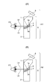
- FIG. 1 The schematic block diagram which shows the 1st, 2nd embodiment of an image display apparatus.
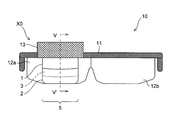
- the front view which shows the spectacles type head mount display provided with the image display apparatus of FIG. 2.
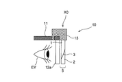
- V-V 'sectional view taken on the line of FIG. The graph which shows the spectral transmission factor of the example of a design of a dielectric multilayer.
- FIG. 1 (A) shows a schematic configuration of an image display apparatus X1 according to the first embodiment in a longitudinal cross section of the main part
- FIG. 1 (B) schematically shows an image display apparatus X2 according to the second embodiment.
- the configuration is shown in the longitudinal section of the main part.
- the image display devices X1 and X2 are optical see-through type image display devices in which the image of the display element 6 is superimposed on an external landscape and projected and displayed on the observer's eye EY, as can be seen from each light path of the image light La and the external light Lb. It has an optical device 5 and a display element 6.
- the display element 6 is an optical device that displays an image by emission of image light La consisting of visible light, and as a specific example thereof, for example, a reflective or transmissive liquid crystal display (LCD), digital -Those including a micromirror device (digital micromirror device), an organic EL (organic electro-luminescence) display, and the like. Furthermore, a lighting device for lighting the display element 6 may be disposed. Examples of the illumination apparatus include an illumination optical system including a light source such as an LED (light emitting diode) and a condensing optical element (lens, mirror, etc.).
- the optical device 5 is joined to act as a plane-parallel plate with respect to the outside light Lb and a combiner 3 for simultaneously guiding the image light La from the display element 6 and the outside light Lb from the outside scenery to the observer eye EY.
- the resin prisms 1 and 2 for supporting the combiner 3 at the bonding surface.
- the two transparent resin prisms 1 and 2 are transparent optical members made of a resin material such as acrylic resin, polycarbonate (PC), and cycloolefin resin.
- the combiner 3 is formed of a dielectric multilayer film having a property of selectively reflecting only light of at least one specific wavelength.
- This dielectric multilayer film comprises alternating layers of low refractive index layers (for example, SiO 2 ) and high refractive index layers (for example, TiO 2 ), and the total number of film layers is 40 or more. Further, the method of forming the dielectric multilayer film includes electron beam evaporation, resistance heating evaporation, ion plating, sputtering and the like.
- the optical device 5 has non-axisymmetric (non-rotationally symmetric) positive optical power in the combiner 3 to thereby direct the image light La from the display element 6 to the observer's eye EY. Act as. As a result, the display image is projected and displayed on the observer's eye EY as a magnified virtual image so that the image of the display element 6 overlaps the external image through the combiner 3.
- the optical power of the combiner 3 can be realized by depositing a dielectric multilayer film on the prism convex surface 1a of the resin prism 1 in the image display device X1, and in the image display device X2, the dielectric is formed on the prism concave surface 2a of the resin prism 2. It can be realized by depositing a multilayer film.
- the image display devices X1 and X2 can be miniaturized.
- curved surfaces such as a conical surface etc., are mentioned, for example.
- the two resin prisms 1 and 2 are bonded with an adhesive 4 so that the combiner 3 consisting of a dielectric multilayer film deposited on one of the two is sandwiched between the prism convex surface 1a and the prism concave surface 2a, and the plane-parallel plate Form. Therefore, it is preferable that the prism convex surface 1a and the prism concave surface 2a have the same shape or substantially the same shape, and it is preferable that the shape of the layer of the adhesive 4 be uniform.
- the resin prism 1 internally guides the image light La incident from the display element 6 by total reflection, and acts to transmit light of an external image (external light Lb). At this time, since the combiner 3 is provided on the bonding surface of the resin prisms 1 and 2, the see-through property (combiner function) of the external image through the bonding surface is secured.
- the resin prism 2 Since the resin prism 2 is joined to the resin prism 1 so as to act as a plane parallel plate to the external light Lb, the external light Lb forms the lower end portion of the resin prism 1 (a curved surface inclined in a substantially wedge shape) It is possible to prevent the distortion when the light is transmitted through the prism 2 from being canceled by the prism 2 and to cause distortion in the observed external image (improved see-through property). Further, since the dielectric multilayer film constituting the combiner 3 is not in direct contact with air by being sandwiched between the prism convex surface 1a and the prism concave surface 2a, even if the humidity fluctuates rapidly, the influence thereof is affected. Is largely mitigated by the resin prisms 1 and 2. As a result, film breakage due to humidity fluctuation is reduced or prevented.
- the water absorption of the resin prisms 1 and 2 is preferably 0.2% or less, and more preferably 0.1% or less.
- the resin material may be deformed (swelled) by water absorption to cause membrane cracking.
- the dielectric multilayer film can be protected from environmental changes, so that film cracking due to humidity fluctuation can be effectively suppressed.
- a low water absorption resin material such as polycarbonate or cycloolefin resin is preferable as a material for the resin prisms 1 and 2 because the water absorption is smaller (water absorption: 0.2% or less) compared to an acrylic resin.
- the dielectric multilayer film constituting the combiner 3 is a notch filter (band stop filter with a narrow stop band) having reflection bands at three wavelengths of three primary colors RGB for colorization. Therefore, as a part of the video light La incident on the combiner 3, the video light La in the reflection band of RGB is reflected.
- the image light La reflected by the combiner 3 is incident on the observer's eye EY together with the external light Lb transmitted through the combiner 3, so the observer observes the external image (high transmittance) well together with the display image. be able to.
- the resin prism 1 which is a transparent base material is configured to totally reflect the image light La from the display element 6 inside and guide the light to the combiner 3, the image light La emitted from the display element 6 is It can be used without waste to provide a bright image to the observer.
- the dielectric multilayer film As described above, by forming the dielectric multilayer film on the prism convex surface 1a or the prism concave surface 2a, it is possible to obtain the combiner 3 which constitutes the positive power concave reflection surface. If it is attempted to form a combiner having the same shape as this with a half mirror, the luminous transmittance will be low and it will be difficult to obtain good see-through performance. Therefore, when using the dielectric multilayer film, it is possible to balance high luminous transmittance of the ambient light Lb and the brightness of the image light La (display image) in a well-balanced manner as compared with the half mirror.
- the dielectric multilayer film since the difference in refractive index can be made large when compared to the hologram optical element, the wavelength fluctuation (that is, the angle dependency) due to the incident angle can be made small, and furthermore, it can be configured thin.
- the ridge line of the is thin and high see-through property is obtained.
- the dielectric multilayer film has a wavelength width larger than that of the hologram optical element, the reflectance (display efficiency) is high. If the wavelength width is small, the see-through property is enhanced, but if the wavelength width is too small, the display efficiency is reduced. On the contrary, if it is going to improve display efficiency, the see-through property (how to see and how to be seen) will fall like half mirror.
- the notch filter is formed of the dielectric multilayer film, but if the same characteristics as the hologram optical element are to be realized by the dielectric multilayer film, the number of layers of the dielectric multilayer film increases and the stress is increased. Is likely to remain. Even if it is attempted to cancel the stress by the combination of the low refractive index layer and the high refractive index layer, the stress remains in the dielectric multilayer film. The residual stress causes film peeling. In particular, when a dielectric multilayer film is formed on a resin-made prism surface, the temperature fluctuation and the humidity fluctuation affect the dielectric multilayer film, so in order to stabilize the dielectric multilayer film, the dielectric multilayer film The residual stress of is desired to be small. However, it is difficult to completely eliminate the residual stress, and the larger the number of layers, the larger the residual amount.
- the stress includes tensile stress and compressive stress, but in the combiner 3 of the image display devices X1 and X2, the bending direction of the dielectric multilayer film due to the residual stress and the bonding surface of the resin prisms 1 and 2 in order to prevent the film peeling. It is aligned so that the direction of bending and the same. That is, the dielectric multilayer film used in the image display apparatus X1 is formed by vapor deposition on the prism convex surface 1a so as to act as a concave reflection surface for the image light La, and has a compressive stress as a residual stress. It has become.
- the dielectric multilayer film used in the image display device X2 is formed by evaporation on the concave surface 2a of the prism so as to act as a concave reflection surface for the image light La, and has a tensile stress as a residual stress. It has become.
- the coating on the prism convex surface 1a or the prism concave surface 2a is stabilized and the film peels off Occurrence is suppressed.
- a dielectric multilayer film having compressive stress as residual stress is formed on the prism convex surface 1a as in the image display device X1, in a direction (sticking direction) where the dielectric multilayer film is to be attached to the prism convex surface 1a. Compressive stress acts.
- the residual stress of the dielectric multilayer film changes with the film density, so its magnitude can be controlled.
- the generation direction of residual stress can also be controlled.
- residual stress in SiO 2 which is a low refractive index material is compressive stress (negative stress)
- residual stress in TiO 2 which is a high refractive index material is Depending on film forming conditions, control from compressive stress (negative stress) to tensile stress (positive stress) is possible.
- the dielectric multilayer film is preferably composed of alternating layers of low refractive index layers and high refractive index layers, and the total number of film layers is preferably 40 or more.
- the total number of film layers is preferably 40 or more.
- the refractive index difference between the low refractive index layer and the high refractive index layer is preferably 0.8 or more, and more preferably 1.0 or more.
- the relationship is also related to the total number of film layers, when the difference in refractive index between the low refractive index layer and the high refractive index layer is small, the number of layers increases and the residual stress increases. And a decrease in reflectance occur. Therefore, it is preferable that the difference in refractive index be large, and by making the difference in refractive index large, it is possible to reduce the wavelength fluctuation (that is, the angle dependency) due to the incident angle.
- the dielectric multilayer film is preferably a notch filter having a reflection band at three wavelengths corresponding to the three primary colors RGB.
- the notch filter is an optical filter that reflects only light of a single wavelength with a predetermined reflectance and transmits the remaining light. Compared with a half mirror, compatibility with light sources such as LEDs, wavelength width, wavelength fluctuation, etc. The efficiency is good.
- the reflection band of the notch filter is preferably 10 nm or more and 50 nm or less in full width at half maximum (FWHM).
- FWHM full width at half maximum
- This dielectric multilayer film is composed of alternating layers (SiO 2 / TiO 2) of low refractive index layers made of SiO 2 and high refractive index layers made of TiO 2 , and the layer numbers are in order from the resin prism 1 side It is attached.
- the material of the resin prism 1 is a cycloolefin resin, and specifically, ZEONEX (registered trademark) E48R (water absorption: less than 0.01%) manufactured by Nippon Zeon Co., Ltd.
- the refractive index difference between the low refractive index layer and the high refractive index layer is 0.83 to 1.2.
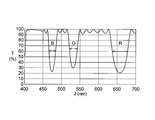
- the graph of FIG. 4 shows the spectral transmittance (%) at an incident angle of 30 ° of this dielectric multilayer film.
- the vertical axis is the transmittance T (%), and the horizontal axis is the wavelength ⁇ (nm).
- the reflection band (FWHM) of the notch filter is B: 17.5 nm, G: 21.2 nm, R: 39.4 nm, and is indicated by a double arrow in FIG.
- the dielectric multilayer film Since the residual stress of the film in each material varies depending on the film forming conditions, it is important to adjust the conditions at the time of film forming. Usually, residual stress in SiO 2 is compressive stress (negative stress), and residual stress in TiO 2 is compressive stress (negative stress). Therefore, since the compressive stress is accumulated, the dielectric multilayer film is formed on the prism convex surface 1a. Since the residual stress in TiO 2 becomes tensile stress (positive stress) depending on film forming conditions, tensile stress may remain as a whole if it can be canceled out well. In that case, the dielectric multilayer film is formed on the prism concave surface 2a.
- SiO 2 / TiO 2 is used, but Al 2 O 3 / TiO 2 , SiO 2 / Al 2 O 3 , SiO 2 / Ti 2 O 5 or a combination of three or more materials may be used.
- PMMA polymethyl methacrylate
- PC polycarbonate
- the maximum moisture absorption in an atmosphere with a relative humidity of 52% is only 0.16%.
- Refractive index for each wavelength of SiO 2 (all absorption coefficients are 0.0) Wavelength (nm) Refractive index 386.41 1.48465 447.05 1.47953 516.07 1.47515 626.05 1.47006 770.22 1.46561
- Refractive index for each wavelength of TiO 2 (all absorption coefficients are 0.0) Wavelength (nm) Refractive index 392.86 2.64429 427.41 2.55972 473.15 2.48053 540.08 2.41239 633.47 2.35690 782.20 2.29537
- the image display devices X1 and X2 described above it is possible to stably obtain a bright and favorable image display while having a high light transmittance and a see-through property while being lightweight and compact.
- the bending direction of the dielectric multilayer film due to the residual stress and the bending direction of the bonding surface of the resin prisms 1 and 2 are aligned, film peeling is suppressed and display image observation and the external world It becomes possible to perform see-through observation favorably and stably.
- the combiner 3 simultaneously guides the image displayed on the display element 6 and the external image to the observer's eye EY, the observer receives the image and the external image provided from the display element 6 through the combiner 3. Can be observed simultaneously. Therefore, by mounting the image display apparatus X1 or X2 described above, it is possible to configure an optical see-through display having a function of projecting and displaying an image on the observer eye EY with the optical device 5 in a see-through manner.
- the optical see-through display is a head mounted display including a support member that supports the image display apparatus X1 (that is, supports in front of the observer's eye) such that the combiner 3 is positioned in front of the observer's eye EY. Is desirable. Since the image display devices X1 and X2 have high see-through properties, high video display effects can be obtained by arranging the video display in front of the observer's eyes.
- a head mounted display HMD
- a head up display HUD
- a spectacles type As a form of a head mounted display, a spectacles type, a helmet type etc. are mentioned.
- a head-up display it is for driving
- the resin prisms 1 and 2 are lighter than glass prisms, they are suitable for wearable displays (head mounted displays etc.). Therefore, an image display device X0 is assumed as a representative example of the image display devices X1 and X2, and an eyeglass-type head mounted display provided with the image display device X0 will be exemplified and described below.
- FIG. 2 shows a schematic configuration of the eyeglass-type head mounted display 10 provided with the image display device X0
- FIG. 3 shows a cross-sectional structure along line V-V '.
- the head mounted display 10 is configured to include the above-described image display device X0, a frame (supporting member) 11, lenses 12a and 12b, and a housing 13.
- the lenses 12 a and 12 b and the housing 13 are supported by a frame 11.
- the display element 6 and the illumination device (not shown) of the image display device X0 are accommodated in the housing 13, and the upper end portion of the optical device 5 which is an eyepiece optical system is also located in the housing 13.
- the main body portion of the optical device 5 is positioned in front (external side) of the lens 12a for the right eye by supporting the housing 13 by the frame 11 (FIG. 3).
- the lenses 12a and 12b may be lenses for spectacles or may be dummy lenses formed of plane parallel plates.
- the display element 6 in the housing 13, a light source (not shown), etc. are connected to a circuit board (not shown) via a cable (not shown) provided penetrating the housing 13 and from the circuit board
- Driving power and video signals are supplied to the display element 6 and the light source.
- the image display device X0 further includes an imaging device for capturing still images and moving images, a microphone, a speaker, an earphone, and the like, and information on the captured image and display image via an external server or terminal and a communication line such as the Internet. And voice information may be exchanged (transmitted / received).
- the head mounted display 10 When the head mounted display 10 is mounted on the head of the observer and an image is displayed on the display element 6 (FIG. 1), the image light La is guided to the observer eye EY through the optical device 5 and the observer The magnified virtual image of the display image of the image display device X0 can be observed. At the same time, the observer can see through the optical device 5 a see-through image of the outside world.
- the observer By supporting the image display device X0 by the frame 11, the observer can observe the display image and the external image provided from the image display device X0 simultaneously and stably for a long time without hands, and the vacant hand Can do the desired work.
- the image may be observed with both eyes using two image display devices X0.
- the above-described embodiment includes the following characteristic configurations (# 1) to (# 9) and the like.
- the junction surface comprises a prism convex surface and a prism concave surface
- the combiner comprises a dielectric multilayer film having a property of selectively reflecting only light of at least one specific wavelength
- the dielectric multilayer film is formed by evaporation on the convex surface of the prism so as to act as a concave reflection surface for the image light, and has a compressive stress as a residual stress, or
- the image display device wherein the dielectric multilayer film is formed on the concave surface of the prism by vapor deposition so as to act as
- the dielectric multilayer film comprises alternating layers of low refractive index layers and high refractive index layers, and the total number of film layers is 40 or more (# 1) Display device.
- (# 3) The image display device according to (# 2), wherein the difference in refractive index between the low refractive index layer and the high refractive index layer is 0.8 or more.
- (# 4) The image display device according to (# 2) or (# 3), wherein the low refractive index layer is SiO 2 and the high refractive index layer is TiO 2 .
- (# 5) The image display device according to any one of (# 1) to (# 4), wherein the water absorption rate of the two resin prisms is 0.2% or less.
- the dielectric multilayer film is a notch filter having a reflection band at three wavelengths corresponding to the three primary colors RGB, described in any one of (# 1) to (# 5). Image display device.
- (# 7) The image display device according to (# 6), wherein the reflection band of the notch filter is 10 nm or more and 50 nm or less in full width at half maximum.
- (# 9) The optical see-through display according to (# 8), comprising a support member for supporting the image display device such that the combiner is positioned in front of the observer's eye.
Landscapes
- Physics & Mathematics (AREA)
- General Physics & Mathematics (AREA)
- Optics & Photonics (AREA)
- Engineering & Computer Science (AREA)
- Multimedia (AREA)
- Signal Processing (AREA)
Abstract
画像表示装置は、表示素子からの映像光と外界風景からの外界光とを同時に観察者眼に導くコンバイナーと、外界光に対して平行平面板として作用するように接合されると共に、その接合面でコンバイナー3を支持する樹脂プリズムと、を有する。接合面はプリズム凸面とプリズム凹面とからなり、コンバイナーは少なくとも1つの特定波長の光のみを選択的に反射する特性を有する誘電体多層膜からなる。誘電体多層膜は、映像光に対して凹面反射面として作用するようにプリズム凸面に蒸着により形成され、かつ、残留応力として圧縮応力を有するか、又は、誘電体多層膜が、映像光に対して凹面反射面として作用するようにプリズム凹面に蒸着により形成され、かつ、残留応力として引っ張り応力を有する。
Description
本発明は画像表示装置と光学シースルーディスプレイに関するものであり、例えば、液晶表示素子の2次元映像をコンバイナーで観察者眼に投影表示する光学シースルー型の画像表示装置と、その画像表示装置を備えた光学シースルーディスプレイ(ヘッドマウントディスプレイ等)に関するものである。
映像のシースルー表示を行うためにコンバイナーを搭載した光学シースルー型の画像表示装置が従来より知られている。例えば特許文献1に記載の画像表示装置では、レリーフ型ホログラムの格子面にコートされたノッチフィルターで所定波長の光を反射させるコンバイナーが搭載されている。
しかし、特許文献1に記載の画像表示装置では、レリーフ型ホログラムとノッチフィルターとの組み合わせがコンバイナーの軽量・薄型化を困難にしている。また、温度・湿度によるホログラム構造の変形がノッチフィルターに与える影響、ノッチフィルターの残留応力による膜剥がれ等が考慮されておらず、画像表示の明るさと外界のシースルー性との両立に関しても考慮されていない。
本発明はこのような状況に鑑みてなされたものであって、その目的は、軽量・コンパクトでありながら、透過率の高いシースルー性を有するとともに明るく良好な画像表示を安定的に得ることが可能な画像表示装置と、それを備えた光学シースルーディスプレイを提供することにある。
上記目的を達成するために、本発明の画像表示装置は、映像を外界風景に重ねて観察者眼に投影表示する光学シースルー型の画像表示装置であって、
前記映像を表示する表示素子と、前記表示素子からの映像光と前記外界風景からの外界光とを同時に観察者眼に導くコンバイナーと、前記外界光に対して平行平面板として作用するように接合されると共に、その接合面で前記コンバイナーを支持する2枚の樹脂プリズムと、を有し、
前記接合面が、プリズム凸面とプリズム凹面とからなり、
前記コンバイナーが、少なくとも1つの特定波長の光のみを選択的に反射する特性を有する誘電体多層膜からなり、
前記誘電体多層膜が、前記映像光に対して凹面反射面として作用するように前記プリズム凸面に蒸着により形成され、かつ、残留応力として圧縮応力を有するか、又は、
前記誘電体多層膜が、前記映像光に対して凹面反射面として作用するように前記プリズム凹面に蒸着により形成され、かつ、残留応力として引っ張り応力を有することを特徴とする。
前記映像を表示する表示素子と、前記表示素子からの映像光と前記外界風景からの外界光とを同時に観察者眼に導くコンバイナーと、前記外界光に対して平行平面板として作用するように接合されると共に、その接合面で前記コンバイナーを支持する2枚の樹脂プリズムと、を有し、
前記接合面が、プリズム凸面とプリズム凹面とからなり、
前記コンバイナーが、少なくとも1つの特定波長の光のみを選択的に反射する特性を有する誘電体多層膜からなり、
前記誘電体多層膜が、前記映像光に対して凹面反射面として作用するように前記プリズム凸面に蒸着により形成され、かつ、残留応力として圧縮応力を有するか、又は、
前記誘電体多層膜が、前記映像光に対して凹面反射面として作用するように前記プリズム凹面に蒸着により形成され、かつ、残留応力として引っ張り応力を有することを特徴とする。
本発明の光学シースルーディスプレイは、本発明の画像表示装置を搭載することにより、前記コンバイナーで前記映像を観察者眼にシースルーで投影表示する機能を備えたことを特徴とする。
本発明によれば、軽量・コンパクトでありながら、透過率の高いシースルー性を有するとともに明るく良好な画像表示を安定的に得ることが可能な画像表示装置と、それを備えた光学シースルーディスプレイを実現することができる。例えば、残留応力による誘電体多層膜の曲がり方向と、樹脂プリズムの接合面の曲がり方向と、が一致するように揃えられているため、膜剥がれが抑制されて、表示画像観察と外界シースルー観察を良好かつ安定的に行うことが可能となる。
以下、本発明を実施した画像表示装置,光学シースルーディスプレイ等を、図面を参照しつつ説明する。なお、各実施の形態等の相互で同一の部分や相当する部分には同一の符号を付して重複説明を適宜省略する。
図1(A)に第1の実施の形態に係る画像表示装置X1の概略構成を要部の縦断面で示し、図1(B)に第2の実施の形態に係る画像表示装置X2の概略構成を要部の縦断面で示す。画像表示装置X1,X2は、映像光La及び外界光Lbの各光路から分かるように、表示素子6の映像を外界風景に重ねて観察者眼EYに投影表示する光学シースルー型の画像表示装置であって、光学デバイス5と表示素子6を有している。
表示素子6は、可視光からなる映像光Laの発光により映像を表示する光学装置であり、その具体例としては、例えば、反射型又は透過型の液晶表示素子(LCD:liquid crystal display),デジタル・マイクロミラー・デバイス(digital micromirror device),有機EL(organic electro-luminescence)ディスプレイ等を含むものが挙げられる。さらに、表示素子6を照明するための照明装置を配置してもよい。照明装置としては、LED(light emitting diode)等の光源,集光用光学素子(レンズ,ミラー等)で構成された照明光学系等を備えたものが挙げられる。
光学デバイス5は、表示素子6からの映像光Laと外界風景からの外界光Lbとを同時に観察者眼EYに導くコンバイナー3と、外界光Lbに対して平行平面板として作用するように接合されると共に、その接合面でコンバイナー3を支持する樹脂プリズム1,2と、を有している。2枚の透明な樹脂プリズム1,2は、アクリル系樹脂,ポリカーボネート(PC),シクロオレフィン樹脂等の樹脂材料で構成された透明な光学部材である。コンバイナー3は、少なくとも1つの特定波長の光のみを選択的に反射する特性を有する誘電体多層膜からなっている。この誘電体多層膜は、低屈折率層(例えばSiO2)と高屈折率層(例えばTiO2)との交互層からなり、その総膜層数は40層以上である。また、誘電体多層膜の形成方法には、電子線ビーム蒸着、抵抗加熱蒸着、イオンプレーティング、スパッタリング等が含まれる。
光学デバイス5は、非軸対称(非回転対称)な正の光学的パワーをコンバイナー3に有しており、それによって表示素子6からの映像光Laを観察者眼EYに導くための接眼光学系として機能する。その結果、コンバイナー3を介して表示素子6の映像が外界像に重なるように、その表示映像が拡大虚像として観察者眼EYにシースルーで投影表示される。コンバイナー3の光学的パワーは、画像表示装置X1では樹脂プリズム1のプリズム凸面1aに誘電体多層膜を蒸着させることにより実現可能であり、画像表示装置X2では樹脂プリズム2のプリズム凹面2aに誘電体多層膜を蒸着させることにより実現可能である。コンバイナー3の光学的パワーを曲面で構成することにより、レンズ等の光学素子を別途配置する必要がなくなるので、画像表示装置X1,X2の小型化が可能になる。なお、接合面を構成するプリズム凸面1aとプリズム凹面2aの具体例としては、例えば円錐面等の曲面が挙げられる。
2枚の樹脂プリズム1,2は、いずれか一方に蒸着された誘電体多層膜からなるコンバイナー3を、プリズム凸面1aとプリズム凹面2aとで挟むようにして接着剤4で接合されて、前記平行平面板を形成している。したがって、プリズム凸面1aとプリズム凹面2aとは同一形状又は略同一形状を有することが好ましく、接着剤4の層の厚さが均一になる形状を有することが好ましい。樹脂プリズム1は、表示素子6から入射してくる映像光Laを全反射により内部で導光する一方、外界像の光(外界光Lb)を透過させるように作用する。その際、樹脂プリズム1,2の接合面上にコンバイナー3が設けられているため、接合面を介した外界像のシースルー性(コンバイナー機能)が確保される。
外界光Lbに対して平行平面板として作用するように、樹脂プリズム2が樹脂プリズム1に接合されているため、外界光Lbが樹脂プリズム1の下端部(略楔状に傾斜した曲面を形成している部分)を透過するときの屈折がプリズム2でキャンセルされて、観察される外界像に歪みが生じるのを防止することができる(シースルー性の向上)。また、コンバイナー3を構成している誘電体多層膜は、プリズム凸面1aとプリズム凹面2aとで挟まれることによって、直接空気に触れない状態にあるため、急激に湿度が変動しても、その影響は樹脂プリズム1,2で大幅に緩和される。その結果、湿度変動による膜割れが低減又は防止される。
樹脂プリズム1,2の吸水率は、0.2%以下であることが好ましく、0.1%以下でであることが更に好ましい。樹脂材料は吸水により変形(膨潤)して、膜割れを生じさせることがある。樹脂プリズム1,2の吸水率が小さいほど、誘電体多層膜を環境変化から守ることができるため、湿度変動による膜割れを効果的に抑制することができる。例えば、ポリカーボネート,シクロオレフィン樹脂等の低吸水率樹脂材料は、アクリル系樹脂に比べて吸水率が小さい(吸水率:0.2%以下)ため、樹脂プリズム1,2の材料として好ましい。前述したように、プリズム凸面1aとプリズム凹面2aとが同一形状又は略同一形状を有する場合、湿度変動の影響をより一層小さくすることができるので、環境変化に強くなる。
コンバイナー3を構成している誘電体多層膜は、カラー化のために3原色RGBの3波長に反射帯域を有するノッチフィルター(阻止帯域が狭いバンドストップフィルター)である。したがって、コンバイナー3に入射した映像光Laの一部として、RGBの反射帯域の映像光Laが反射される。コンバイナー3で反射した映像光Laは、コンバイナー3を透過した外界光Lbと共に、観察者眼EYに入射することになるので、観察者は表示映像と共に外界像(高透過率)も良好に観察することができる。また、透明基材である樹脂プリズム1は、表示素子6からの映像光Laを内部で全反射させてコンバイナー3に導光する構成になっているため、表示素子6から発光した映像光Laを無駄なく利用して、観察者に明るい映像を提供することができる。
上述したように、プリズム凸面1a又はプリズム凹面2a上に誘電体多層膜を形成することにより、正パワーの凹面反射面を構成するコンバイナー3を得ることができる。これと同一形状のコンバイナーをハーフミラーで構成しようとすると、視感度透過率が低くなって、良好なシースルー性を得ることが困難になる。したがって、ハーフミラーと比較した場合、誘電体多層膜を用いると、外界光Lbの高視感度透過率と映像光La(表示画像)の明るさとをバランス良く両立させることが可能になる。
誘電体多層膜では、ホログラム光学素子と比較した場合、屈折率差を大きくとることができるので、入射角度による波長変動(すなわち角度依存性)を小さくすることができ、しかも薄く構成できるので、接合の稜線が細くなって高いシースルー性が得られる。また、誘電体多層膜はホログラム光学素子よりも波長幅が大きいので、反射率(表示効率)は高くなる。波長幅が小さいとシースルー性は高くなるが、波長幅が小さすぎると表示効率が低下する。逆に表示効率を向上させようとすると、ハーフミラーと同様、シースルー性(見え方や見られ方)が低下してしまう。
コンバイナー3では、誘電体多層膜で前記ノッチフィルターを構成しているが、ホログラム光学素子と同様の特性を誘電体多層膜で実現しようとすれば、誘電体多層膜の層数が多くなって応力が残りやすくなる。低屈折率層と高屈折率層との組み合わせにより応力をキャンセルしようとしても、誘電体多層膜には応力が残留する。その残留応力は膜はがれの原因となる。特に樹脂製のプリズム面の上に誘電体多層膜が形成される場合、温度変動や湿度変動が誘電体多層膜に影響するため、誘電体多層膜の安定化を図るうえで、誘電体多層膜の残留応力は小さいことが望まれる。しかし、残留応力を完全に消すことは難しく、層数が多いほど残留量も大きくなる。
応力には引っ張り応力と圧縮応力があるが、画像表示装置X1,X2のコンバイナー3では、膜はがれを防止するため、残留応力による誘電体多層膜の曲がり方向と、樹脂プリズム1,2の接合面の曲がり方向と、が一致するように揃えられている。つまり、画像表示装置X1に用いられている誘電体多層膜は、映像光Laに対して凹面反射面として作用するようにプリズム凸面1aに蒸着により形成され、かつ、残留応力として圧縮応力を有する構成になっている。また、画像表示装置X2に用いられている誘電体多層膜は、映像光Laに対して凹面反射面として作用するようにプリズム凹面2aに蒸着により形成され、かつ、残留応力として引っ張り応力を有する構成になっている。
上記のように、残留応力による誘電体多層膜の曲がり方向と、樹脂プリズム1,2の接合面の曲がり方向と、が一致すると、プリズム凸面1a又はプリズム凹面2aへのコーティングが安定化し、膜はがれの発生が抑制される。例えば画像表示装置X1のように、残留応力として圧縮応力を有する誘電体多層膜をプリズム凸面1aに形成した場合、誘電体多層膜がプリズム凸面1aに引っ付こうとする方向(貼り付く方向)に圧縮応力が作用する。また画像表示装置X2のように、残留応力として引っ張り応力を有する誘電体多層膜をプリズム凹面2aに形成した場合、誘電体多層膜がプリズム凹面2aに引っ付こうとする方向(貼り付く方向)に引っ張り応力が作用する。したがって、いずれの場合も残留応力は誘電体多層膜が剥離しない方向に作用することになる。
誘電体多層膜の残留応力は膜密度により変化するため、その大きさは制御可能である。また、残留応力の発生方向も制御可能であり、例えば、低屈折率材料であるSiO2での残留応力は圧縮応力(負応力)であり、高屈折率材料であるTiO2での残留応力は製膜条件により圧縮応力(負応力)から引っ張り応力(正応力)まで制御可能である。
誘電体多層膜は、低屈折率層と高屈折率層との交互層からなり、総膜層数が40層以上であることが好ましい。誘電体多層膜の設計上、3原色RGBに対応した3波長に反射帯域を有するノッチフィルターを設計するには、ある程度の層数が必要である。層数が少ないと、透過部分の透過率が下がったり(シースルー性)、反射部分の帯域が狭くなったり(シースルー性)、反射部分の反射率(明るさ)が低くなったりする、という不具合があるので、総膜層数が40層以上であることが好ましい。
低屈折率層と高屈折率層との屈折率差は、0.8以上であることが好ましく、1.0以上であることが更に好ましい。上記総膜層数とも関係するが、低屈折率層と高屈折率層との屈折率差が小さいと、層数が増えるため残留応力が大きくなり、層数が同じであれば透過率の低下や反射率の低下等が発生する。そのため、屈折率の差は大きい方が好ましく、屈折率差を大きくすることにより、入射角度による波長変動(すなわち角度依存性)を小さくすることができる。
誘電体多層膜は、前述したように、3原色RGBに対応した3波長に反射帯域を有するノッチフィルターであることが好ましい。ノッチフィルターは、単一波長の光のみを所定の反射率で反射させ、残りの光は透過させる光学フィルターであり、ハーフミラーと比較すると、LED等の光源との相性、波長幅、波長変動等に関して効率が良い。
ノッチフィルターの反射帯域は、半値全幅(FWHM:Full Width at Half Maximum)で10nm以上50nm以下であることが好ましい。反射帯域が50nmを上回るとシースル性が低下し、反射帯域が10nmを下回るとLED等の光源の光利用効率が低下して暗くなる。
誘電体多層膜(ノッチフィルター)の設計例と、膜材料であるSiO2,TiO2の波長ごとの屈折率と、を以下に示す。この誘電体多層膜は、SiO2からなる低屈折率層と、TiO2からなる高屈折率層と、の交互層(SiO2/TiO2)で構成されており、層番号は樹脂プリズム1側から順に付してある。樹脂プリズム1の材料はシクロオレフィン樹脂であり、具体的には日本ゼオン(株)製 ZEONEX(登録商標) E48R(吸水率:0.01%未満)である。また、低屈折率層と高屈折率層との屈折率差は0.83~1.2である。
図4のグラフに、この誘電体多層膜の入射角度30°での分光透過率(%)を示す。図4のグラフにおいて、縦軸は透過率T(%)であり、横軸は波長λ(nm)である。ノッチフィルターの反射帯域(FWHM)は、B:17.5nm,G:21.2nm,R:39.4nmであり、図4中に両矢印で示す。
各材料における膜の残留応力は製膜条件によって変動するので、製膜時の条件調整が重要である。通常、SiO2での残留応力は圧縮応力(負応力)であり、TiO2も残留応力は圧縮応力(負応力)である。したがって、圧縮応力がたまっていくので、誘電体多層膜はプリズム凸面1aに形成する。TiO2での残留応力は製膜条件によっては引っ張り応力(正応力)になるので、うまく打ち消せると全体的に引っ張り応力が残ることもある。その場合、誘電体多層膜はプリズム凹面2aに形成する。
この設計例ではSiO2/TiO2であるが、Al2O3/TiO2,SiO2/Al2O3,SiO2/Ti2O5や3つ以上の材料の組み合わせでも構わない。また、アクリル系樹脂であるPMMA(polymethyl methacrylate)の吸水率は、0.3%(JIS K7209)である。PC(polycarbonate)の吸水率に関しては、相対湿度52%の雰囲気中の最大吸湿量が僅かに0.16%である。
誘電体多層膜(ノッチフィルター)の設計例
層番号 材料 膜厚(nm)
1 TiO2 23.79
2 SiO2 21.84
3 TiO2 79.42
4 SiO2 25.87
5 TiO2 31.39
6 SiO2 44.78
7 TiO2 118.68
8 SiO2 67.37
9 TiO2 26.08
10 SiO2 42.75
11 TiO2 128.37
12 SiO2 32.01
13 TiO2 53.55
14 SiO2 18.49
15 TiO2 64.17
16 SiO2 48.29
17 TiO2 23.02
18 SiO2 41.02
19 TiO2 69.03
20 SiO2 39.24
21 TiO2 26.46
22 SiO2 49.87
23 TiO2 64.57
24 SiO2 22.28
25 TiO2 46.51
26 SiO2 37.70
27 TiO2 41.96
28 SiO2 24.62
29 TiO2 60.11
30 SiO2 37.98
31 TiO2 44.50
32 SiO2 34.81
33 TiO2 121.52
34 SiO2 40.38
35 TiO2 126.77
36 SiO2 74.95
37 TiO2 20.22
38 SiO2 35.28
39 TiO2 64.18
40 SiO2 49.27
41 TiO2 18.58
42 SiO2 64.47
43 TiO2 59.00
44 SiO2 15.46
45 TiO2 48.83
46 SiO2 166.89
47 TiO2 135.17
48 SiO2 11.82
49 TiO2 97.53
50 SiO2 59.85
51 TiO2 20.19
52 SiO2 36.30
53 TiO2 67.45
54 SiO2 34.92
55 TiO2 25.86
56 SiO2 61.02
57 TiO2 40.96
58 SiO2 18.28
59 TiO2 60.68
60 SiO2 181.94
61 TiO2 97.49
62 SiO2 37.02
層番号 材料 膜厚(nm)
1 TiO2 23.79
2 SiO2 21.84
3 TiO2 79.42
4 SiO2 25.87
5 TiO2 31.39
6 SiO2 44.78
7 TiO2 118.68
8 SiO2 67.37
9 TiO2 26.08
10 SiO2 42.75
11 TiO2 128.37
12 SiO2 32.01
13 TiO2 53.55
14 SiO2 18.49
15 TiO2 64.17
16 SiO2 48.29
17 TiO2 23.02
18 SiO2 41.02
19 TiO2 69.03
20 SiO2 39.24
21 TiO2 26.46
22 SiO2 49.87
23 TiO2 64.57
24 SiO2 22.28
25 TiO2 46.51
26 SiO2 37.70
27 TiO2 41.96
28 SiO2 24.62
29 TiO2 60.11
30 SiO2 37.98
31 TiO2 44.50
32 SiO2 34.81
33 TiO2 121.52
34 SiO2 40.38
35 TiO2 126.77
36 SiO2 74.95
37 TiO2 20.22
38 SiO2 35.28
39 TiO2 64.18
40 SiO2 49.27
41 TiO2 18.58
42 SiO2 64.47
43 TiO2 59.00
44 SiO2 15.46
45 TiO2 48.83
46 SiO2 166.89
47 TiO2 135.17
48 SiO2 11.82
49 TiO2 97.53
50 SiO2 59.85
51 TiO2 20.19
52 SiO2 36.30
53 TiO2 67.45
54 SiO2 34.92
55 TiO2 25.86
56 SiO2 61.02
57 TiO2 40.96
58 SiO2 18.28
59 TiO2 60.68
60 SiO2 181.94
61 TiO2 97.49
62 SiO2 37.02
SiO2の波長ごとの屈折率(吸収係数は全て0.0である。)
波長(nm) 屈折率
386.41 1.48465
447.05 1.47953
516.07 1.47515
626.05 1.47006
770.22 1.46561
波長(nm) 屈折率
386.41 1.48465
447.05 1.47953
516.07 1.47515
626.05 1.47006
770.22 1.46561
TiO2の波長ごとの屈折率(吸収係数は全て0.0である。)
波長(nm) 屈折率
392.86 2.64429
427.41 2.55972
473.15 2.48053
540.08 2.41239
633.47 2.35690
782.20 2.29537
波長(nm) 屈折率
392.86 2.64429
427.41 2.55972
473.15 2.48053
540.08 2.41239
633.47 2.35690
782.20 2.29537
以上説明した画像表示装置X1,X2によれば、軽量・コンパクトでありながら、透過率の高いシースルー性を有するとともに明るく良好な画像表示を安定的に得ることが可能である。例えば、残留応力による誘電体多層膜の曲がり方向と、樹脂プリズム1,2の接合面の曲がり方向と、が一致するように揃えられているため、膜剥がれが抑制されて、表示画像観察と外界シースルー観察を良好かつ安定的に行うことが可能となる。
前述したように、コンバイナー3は表示素子6に表示される映像と外界像とを同時に観察者眼EYに導くので、観察者はコンバイナー3を介して表示素子6から提供される映像と外界像とを同時に観察することができる。したがって、上述した画像表示装置X1又はX2を搭載することにより、光学デバイス5で映像を観察者眼EYにシースルーで投影表示する機能を備えた光学シースルーディスプレイを構成することができる。
上記のように、光学シースルーディスプレイにおいて画像表示装置X1又はX2を搭載することにより、コンバイナー3で映像を観察者眼EYにシースルーで投影表示する機能を備えることが望ましい。また、その光学シースルーディスプレイは、コンバイナー3が観察者眼EYの前方に位置するように画像表示装置X1を支持する(つまり、観察者の眼前で支持する)支持部材を備えたヘッドマウントディスプレイであることが望ましい。画像表示装置X1,X2はシースルー性が高いため、観察者の眼前で映像を表示する配置にすれば、高い映像表示効果を得ることができる。
光学シースルーディスプレイとしては、ヘッドマウントディスプレイ(HMD),ヘッドアップディスプレイ(HUD)等が挙げられる。また、ヘッドマウントディスプレイの形態としては眼鏡型,ヘルメット型等が挙げられ、ヘッドアップディスプレイの用途としては自動車の運転用,飛行機の操縦用等が挙げられる。樹脂プリズム1,2はガラスプリズムに比べて軽量であることから、ウェアラブルディスプレイ(ヘッドマウントディスプレイ等)用として好適である。そこで、前記画像表示装置X1,X2の代表例として画像表示装置X0を想定し、画像表示装置X0を備えた眼鏡型のヘッドマウントディスプレイを例示して以下に説明する。
図2に、画像表示装置X0を備えた眼鏡型のヘッドマウントディスプレイ10の概略構成を示し、図3にそのV-V’線断面構造を示す。ヘッドマウントディスプレイ10は、上述した画像表示装置X0と、フレーム(支持部材)11と、レンズ12a,12bと、筐体13と、を備えた構成になっている。レンズ12a,12bと筐体13は、フレーム11で支持されている。画像表示装置X0の表示素子6や照明装置(不図示)等は、筐体13内に収容されており、接眼光学系である光学デバイス5の上端部も筐体13内に位置している。したがって、筐体13がフレーム11で支持されることにより、光学デバイス5の本体部分は右眼用のレンズ12aの前方(外界側)に位置することになる(図3)。なお、レンズ12a,12bは眼鏡用レンズでもよく、平行平面板からなるダミーレンズでもよい。
筐体13内の表示素子6,光源(不図示)等は、筐体13を貫通して設けられるケーブル(不図示)を介して、回路基板(不図示)と接続されており、回路基板から表示素子6,光源等に駆動電力や映像信号が供給される。なお、画像表示装置X0は、静止画や動画を撮影する撮像装置,マイク,スピーカー,イヤホン等をさらに備え、外部のサーバーや端末とインターネット等の通信回線を介して、撮像画像及び表示画像の情報や音声情報をやりとり(送受信)する構成であってもよい。
ヘッドマウントディスプレイ10を観察者の頭部に装着し、表示素子6(図1)に映像を表示すると、その映像光Laが光学デバイス5を介して観察者眼EYに導かれて、観察者は、画像表示装置X0の表示映像の拡大虚像を観察することができる。また、これと同時に、観察者は光学デバイス5を介して、外界像をシースルーで観察することができる。画像表示装置X0がフレーム11で支持されることにより、観察者は画像表示装置X0から提供される表示映像と外界像とを同時にハンズフリーで長時間安定して観察することができ、空いた手で所望の作業を行うことができる。なお、画像表示装置X0を2つ用いて両眼で映像を観察できるようにしてもよい。
以上の説明から分かるように、上述した実施の形態には以下の特徴的な構成(#1)~(#9)等が含まれている。
(#1):映像を外界風景に重ねて観察者眼に投影表示する光学シースルー型の画像表示装置であって、
前記映像を表示する表示素子と、前記表示素子からの映像光と前記外界風景からの外界光とを同時に観察者眼に導くコンバイナーと、前記外界光に対して平行平面板として作用するように接合されると共に、その接合面で前記コンバイナーを支持する2枚の樹脂プリズムと、を有し、
前記接合面が、プリズム凸面とプリズム凹面とからなり、
前記コンバイナーが、少なくとも1つの特定波長の光のみを選択的に反射する特性を有する誘電体多層膜からなり、
前記誘電体多層膜が、前記映像光に対して凹面反射面として作用するように前記プリズム凸面に蒸着により形成され、かつ、残留応力として圧縮応力を有するか、又は、
前記誘電体多層膜が、前記映像光に対して凹面反射面として作用するように前記プリズム凹面に蒸着により形成され、かつ、残留応力として引っ張り応力を有することを特徴とする画像表示装置。
前記映像を表示する表示素子と、前記表示素子からの映像光と前記外界風景からの外界光とを同時に観察者眼に導くコンバイナーと、前記外界光に対して平行平面板として作用するように接合されると共に、その接合面で前記コンバイナーを支持する2枚の樹脂プリズムと、を有し、
前記接合面が、プリズム凸面とプリズム凹面とからなり、
前記コンバイナーが、少なくとも1つの特定波長の光のみを選択的に反射する特性を有する誘電体多層膜からなり、
前記誘電体多層膜が、前記映像光に対して凹面反射面として作用するように前記プリズム凸面に蒸着により形成され、かつ、残留応力として圧縮応力を有するか、又は、
前記誘電体多層膜が、前記映像光に対して凹面反射面として作用するように前記プリズム凹面に蒸着により形成され、かつ、残留応力として引っ張り応力を有することを特徴とする画像表示装置。
(#2):前記誘電体多層膜が、低屈折率層と高屈折率層との交互層からなり、総膜層数が40層以上であることを特徴とする(#1)記載の画像表示装置。
(#3):前記低屈折率層と前記高屈折率層との屈折率差が0.8以上であることを特徴とする(#2)記載の画像表示装置。
(#4):前記低屈折率層がSiO2であり、前記高屈折率層がTiO2であることを特徴とする(#2)又は(#3)記載の画像表示装置。
(#5):前記2枚の樹脂プリズムの吸水率が0.2%以下であることを特徴とする(#1)~(#4)のいずれか1項に記載の画像表示装置。
(#6):前記誘電体多層膜が、3原色RGBに対応した3波長に反射帯域を有するノッチフィルターであることを特徴とする(#1)~(#5)のいずれか1項に記載の画像表示装置。
(#7):前記ノッチフィルターの反射帯域が半値全幅で10nm以上50nm以下であることを特徴とする(#6)記載の画像表示装置。
(#8):(#1)~(#7)のいずれか1項に記載の画像表示装置を搭載することにより、前記コンバイナーで前記映像を観察者眼にシースルーで投影表示する機能を備えたことを特徴とする光学シースルーディスプレイ。
(#9):前記コンバイナーが観察者眼の前方に位置するように前記画像表示装置を支持する支持部材を備えたことを特徴とする(#8)記載の光学シースルーディスプレイ。
X0,X1,X2 画像表示装置
1,2 樹脂プリズム
1a プリズム凸面(接合面)
2a プリズム凹面(接合面)
3 コンバイナー(誘電体多層膜)
4 接着剤
5 光学デバイス
6 表示素子
10 ヘッドマウントディスプレイ(光学シースルーディスプレイ)
11 フレーム(支持部材)
12a,12b レンズ
13 筐体
La 映像光
Lb 外界光
EY 観察者眼
1,2 樹脂プリズム
1a プリズム凸面(接合面)
2a プリズム凹面(接合面)
3 コンバイナー(誘電体多層膜)
4 接着剤
5 光学デバイス
6 表示素子
10 ヘッドマウントディスプレイ(光学シースルーディスプレイ)
11 フレーム(支持部材)
12a,12b レンズ
13 筐体
La 映像光
Lb 外界光
EY 観察者眼
Claims (9)
- 映像を外界風景に重ねて観察者眼に投影表示する光学シースルー型の画像表示装置であって、
前記映像を表示する表示素子と、前記表示素子からの映像光と前記外界風景からの外界光とを同時に観察者眼に導くコンバイナーと、前記外界光に対して平行平面板として作用するように接合されると共に、その接合面で前記コンバイナーを支持する2枚の樹脂プリズムと、を有し、
前記接合面が、プリズム凸面とプリズム凹面とからなり、
前記コンバイナーが、少なくとも1つの特定波長の光のみを選択的に反射する特性を有する誘電体多層膜からなり、
前記誘電体多層膜が、前記映像光に対して凹面反射面として作用するように前記プリズム凸面に蒸着により形成され、かつ、残留応力として圧縮応力を有するか、又は、
前記誘電体多層膜が、前記映像光に対して凹面反射面として作用するように前記プリズム凹面に蒸着により形成され、かつ、残留応力として引っ張り応力を有する画像表示装置。 - 前記誘電体多層膜が、低屈折率層と高屈折率層との交互層からなり、総膜層数が40層以上である請求項1記載の画像表示装置。
- 前記低屈折率層と前記高屈折率層との屈折率差が0.8以上である請求項2記載の画像表示装置。
- 前記低屈折率層がSiO2であり、前記高屈折率層がTiO2である請求項2又は3記載の画像表示装置。
- 前記2枚の樹脂プリズムの吸水率が0.2%以下である請求項1~4のいずれか1項に記載の画像表示装置。
- 前記誘電体多層膜が、3原色RGBに対応した3波長に反射帯域を有するノッチフィルターである請求項1~5のいずれか1項に記載の画像表示装置。
- 前記ノッチフィルターの反射帯域が半値全幅で10nm以上50nm以下である請求項6記載の画像表示装置。
- 請求項1~7のいずれか1項に記載の画像表示装置を搭載することにより、前記コンバイナーで前記映像を観察者眼にシースルーで投影表示する機能を備えた光学シースルーディスプレイ。
- 前記コンバイナーが観察者眼の前方に位置するように前記画像表示装置を支持する支持部材を備えた請求項8記載の光学シースルーディスプレイ。
Applications Claiming Priority (2)
| Application Number | Priority Date | Filing Date | Title |
|---|---|---|---|
| JP2017-227979 | 2017-11-28 | ||
| JP2017227979 | 2017-11-28 |
Publications (1)
| Publication Number | Publication Date |
|---|---|
| WO2019106969A1 true WO2019106969A1 (ja) | 2019-06-06 |
Family
ID=66663889
Family Applications (1)
| Application Number | Title | Priority Date | Filing Date |
|---|---|---|---|
| PCT/JP2018/037793 Ceased WO2019106969A1 (ja) | 2017-11-28 | 2018-10-10 | 画像表示装置と光学シースルーディスプレイ |
Country Status (1)
| Country | Link |
|---|---|
| WO (1) | WO2019106969A1 (ja) |
Cited By (2)
| Publication number | Priority date | Publication date | Assignee | Title |
|---|---|---|---|---|
| US20220276476A1 (en) * | 2021-02-26 | 2022-09-01 | Seiko Epson Corporation | Optical unit and image display device |
| JP2022146930A (ja) * | 2021-03-22 | 2022-10-05 | 三星電子株式会社 | 非対称的な倍率を有するコンバイナを含むディスプレイ装置 |
Citations (6)
| Publication number | Priority date | Publication date | Assignee | Title |
|---|---|---|---|---|
| JPS62502150A (ja) * | 1985-08-14 | 1987-08-20 | ヒュ−ズ・エアクラフト・カンパニ− | グレ−デツドインデツクス非球面コンバイナ−及びそれを用いたデイスプレイ システム |
| JPH08307008A (ja) * | 1995-04-28 | 1996-11-22 | Hewlett Packard Co <Hp> | 多層膜構造および面発光レーザ |
| US5734359A (en) * | 1994-07-01 | 1998-03-31 | B.V. Optische Industrie "De Oude Delft" | Display system intended to be attached to the head or to a helmet, and a helmet provided with such a display system |
| JP2006003872A (ja) * | 2004-05-17 | 2006-01-05 | Nikon Corp | 光学素子、コンバイナ光学系、及び情報表示装置 |
| JP2013127489A (ja) * | 2010-03-29 | 2013-06-27 | Panasonic Corp | シースルーディスプレイ |
| JP2016180938A (ja) * | 2015-03-25 | 2016-10-13 | セイコーエプソン株式会社 | 虚像表示装置 |
-
2018
- 2018-10-10 WO PCT/JP2018/037793 patent/WO2019106969A1/ja not_active Ceased
Patent Citations (6)
| Publication number | Priority date | Publication date | Assignee | Title |
|---|---|---|---|---|
| JPS62502150A (ja) * | 1985-08-14 | 1987-08-20 | ヒュ−ズ・エアクラフト・カンパニ− | グレ−デツドインデツクス非球面コンバイナ−及びそれを用いたデイスプレイ システム |
| US5734359A (en) * | 1994-07-01 | 1998-03-31 | B.V. Optische Industrie "De Oude Delft" | Display system intended to be attached to the head or to a helmet, and a helmet provided with such a display system |
| JPH08307008A (ja) * | 1995-04-28 | 1996-11-22 | Hewlett Packard Co <Hp> | 多層膜構造および面発光レーザ |
| JP2006003872A (ja) * | 2004-05-17 | 2006-01-05 | Nikon Corp | 光学素子、コンバイナ光学系、及び情報表示装置 |
| JP2013127489A (ja) * | 2010-03-29 | 2013-06-27 | Panasonic Corp | シースルーディスプレイ |
| JP2016180938A (ja) * | 2015-03-25 | 2016-10-13 | セイコーエプソン株式会社 | 虚像表示装置 |
Cited By (3)
| Publication number | Priority date | Publication date | Assignee | Title |
|---|---|---|---|---|
| US20220276476A1 (en) * | 2021-02-26 | 2022-09-01 | Seiko Epson Corporation | Optical unit and image display device |
| US12259535B2 (en) * | 2021-02-26 | 2025-03-25 | Seiko Epson Corporation | Optical unit and image display device |
| JP2022146930A (ja) * | 2021-03-22 | 2022-10-05 | 三星電子株式会社 | 非対称的な倍率を有するコンバイナを含むディスプレイ装置 |
Similar Documents
| Publication | Publication Date | Title |
|---|---|---|
| EP3754412B1 (en) | Wearable ar system and ar display device | |
| EP2639623B1 (en) | Image display device and image generating device | |
| US10054795B2 (en) | Image display apparatus and head mounted display | |
| CN102298211B (zh) | 光学器件、图像显示设备和头部安装式显示单元 | |
| US7826113B2 (en) | Joined optical member, image display apparatus, and head-mounted display | |
| CN104903774B (zh) | 用于近眼显示器的光组合器 | |
| CN101750738B (zh) | 头戴式显示器 | |
| US9400389B2 (en) | Virtual image display device | |
| TWI836161B (zh) | 用於偏振加擾的光導光學元件 | |
| JP2015184560A (ja) | 導光装置、画像表示装置及び表示装置 | |
| KR102642282B1 (ko) | 도광판 및 화상 표시 장치 | |
| JP2023014127A (ja) | 導光板、画像表示装置 | |
| JP2015184561A (ja) | 導光装置、画像表示装置及び表示装置 | |
| CN217982020U (zh) | 光照度可调的ar眼镜 | |
| WO2005111669A1 (ja) | 光学素子、コンバイナ光学系、及び画像表示装置 | |
| JP2015177405A (ja) | 表示装置及び光学装置 | |
| CN104698588A (zh) | 虚像显示装置 | |
| CN1637459A (zh) | 可戴的彩色显示系统 | |
| JP2020024245A (ja) | 虚像表示装置 | |
| JP7027748B2 (ja) | 虚像表示装置 | |
| WO2019106969A1 (ja) | 画像表示装置と光学シースルーディスプレイ | |
| WO2018043254A1 (ja) | 映像表示装置と光学シースルーディスプレイ | |
| JP2020091449A (ja) | 画像表示装置およびヘッドマウントディスプレイ | |
| JP2013061594A (ja) | 虚像表示装置及び虚像表示装置の製造方法 | |
| WO2017033975A1 (ja) | ホログラム記録構造,光学デバイス及び製造方法 |
Legal Events
| Date | Code | Title | Description |
|---|---|---|---|
| 121 | Ep: the epo has been informed by wipo that ep was designated in this application |
Ref document number: 18884027 Country of ref document: EP Kind code of ref document: A1 |
|
| NENP | Non-entry into the national phase |
Ref country code: DE |
|
| 122 | Ep: pct application non-entry in european phase |
Ref document number: 18884027 Country of ref document: EP Kind code of ref document: A1 |
|
| NENP | Non-entry into the national phase |
Ref country code: JP |