WO2019098049A1 - ひずみゲージ - Google Patents
ひずみゲージ Download PDFInfo
- Publication number
- WO2019098049A1 WO2019098049A1 PCT/JP2018/040744 JP2018040744W WO2019098049A1 WO 2019098049 A1 WO2019098049 A1 WO 2019098049A1 JP 2018040744 W JP2018040744 W JP 2018040744W WO 2019098049 A1 WO2019098049 A1 WO 2019098049A1
- Authority
- WO
- WIPO (PCT)
- Prior art keywords
- resistor
- strain gauge
- resistance portion
- substrate
- gauge according
- Prior art date
- Legal status (The legal status is an assumption and is not a legal conclusion. Google has not performed a legal analysis and makes no representation as to the accuracy of the status listed.)
- Ceased
Links
Images


Classifications
-
- G—PHYSICS
- G01—MEASURING; TESTING
- G01B—MEASURING LENGTH, THICKNESS OR SIMILAR LINEAR DIMENSIONS; MEASURING ANGLES; MEASURING AREAS; MEASURING IRREGULARITIES OF SURFACES OR CONTOURS
- G01B7/00—Measuring arrangements characterised by the use of electric or magnetic techniques
- G01B7/16—Measuring arrangements characterised by the use of electric or magnetic techniques for measuring the deformation in a solid, e.g. by resistance strain gauge
- G01B7/18—Measuring arrangements characterised by the use of electric or magnetic techniques for measuring the deformation in a solid, e.g. by resistance strain gauge using change in resistance
-
- G—PHYSICS
- G01—MEASURING; TESTING
- G01B—MEASURING LENGTH, THICKNESS OR SIMILAR LINEAR DIMENSIONS; MEASURING ANGLES; MEASURING AREAS; MEASURING IRREGULARITIES OF SURFACES OR CONTOURS
- G01B7/00—Measuring arrangements characterised by the use of electric or magnetic techniques
- G01B7/16—Measuring arrangements characterised by the use of electric or magnetic techniques for measuring the deformation in a solid, e.g. by resistance strain gauge
- G01B7/18—Measuring arrangements characterised by the use of electric or magnetic techniques for measuring the deformation in a solid, e.g. by resistance strain gauge using change in resistance
- G01B7/20—Measuring arrangements characterised by the use of electric or magnetic techniques for measuring the deformation in a solid, e.g. by resistance strain gauge using change in resistance formed by printed-circuit technique
Definitions
- the present invention relates to strain gauges.
- the strain gauge which is attached to a measurement object to detect a strain of the measurement object.
- the strain gauge includes a resistor that detects strain, and a material containing, for example, Cr (chromium) or Ni (nickel) is used as a material of the resistor.
- the resistor is formed, for example, on one surface of a base material made of an insulating resin (see, for example, Patent Document 1).
- the present invention has been made in view of the above-described points, and an object of the present invention is to provide a strain gauge which can detect not only the strain on the surface of the object to be measured but also strains other than the surface.
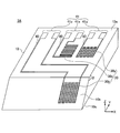
- FIG. 1 is a perspective view illustrating a strain gauge according to a first embodiment.
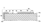
- FIG. 2 is a cross-sectional view illustrating the strain gauge according to the first embodiment, and shows a cross-section cut along a line AA in FIG. 1 in a direction parallel to the YZ plane.
- the strain gauge 1 includes a base 10, a resistor 30 (resistors 30x, 30y, and 30z), and terminals 41 (terminals 41x, 41y, and 41z). Have.
- the side on which the resistance portion 30 x of the base 10 is provided is the upper side or one side, and the side opposite to the side on which the resistance portion 30 x is provided is the lower side. Or on the other side.
- the surface on the side where the resistance portion 30x of each portion is provided is referred to as one surface or the upper surface, and the surface opposite to the side where the resistance unit 30x is provided is referred to as the other surface or the lower surface.
- the strain gauge 1 can be used in the upside-down state or can be disposed at any angle.
- planar view refers to viewing the object in the normal direction of the upper surface 10a of the base material
- planar shape refers to a shape of the object viewed in the normal direction of the upper surface 10a of the base 10 I assume.
- the base 10 is a member to be a base layer for forming the resistance portion 30x and the like, and has flexibility.
- the thickness of the substrate 10 is not particularly limited and may be appropriately selected depending on the purpose. For example, the thickness may be about 5 ⁇ m to 1000 ⁇ m. In particular, when the thickness of the substrate 10 is 5 ⁇ m to 200 ⁇ m, in terms of the transmission of strain from the surface of the strain-generating body bonded to the lower surface of the substrate 10 via the adhesive layer etc., and dimensional stability to the environment.
- the thickness is preferably 10 ⁇ m or more, further preferably in terms of insulation.
- the substrate 10 is made of, for example, PI (polyimide) resin, epoxy resin, PEEK (polyether ether ketone) resin, PEN (polyethylene naphthalate) resin, PET (polyethylene terephthalate) resin, PPS (polyphenylene sulfide) resin, polyolefin resin, etc.
- PI polyimide
- epoxy resin epoxy resin
- PEEK polyether ether ketone
- PEN polyethylene naphthalate
- PET polyethylene terephthalate
- PPS polyphenylene sulfide
- the substrate 10 may be formed of, for example, an insulating resin film containing a filler such as silica or alumina.
- the resistor 30 is a sensing part which is formed on the base material 10 and receives strain to cause resistance change.
- Resistor 30 includes resistors 30x, 30y and 30z. That is, the resistor 30 is a generic name of the resistors 30x, 30y and 30z, and the resistors 30x, 30y and 30z are referred to as the resistor 30 when it is not necessary to distinguish them.
- the resistance portions 30x, 30y, and 30z are shown in a satin pattern.
- the resistance portion 30x is a thin film formed in a predetermined pattern on the base material 10, and is a sensing portion that receives strain and causes a change in resistance.
- the resistance portion 30 x may be formed directly on the upper surface 10 a of the base 10 or may be formed on the upper surface 10 a of the base 10 via another layer.
- FIG. 1 is a three-dimensional orthogonal coordinate system in which the grid direction of the resistance portion 30x is the X direction. Therefore, the resistor 30x can detect strain in the X direction.
- the resistance portion 30y is a thin film formed in a predetermined pattern on the base material 10, and is a sensing portion that receives strain and causes a change in resistance.
- the resistance portion 30 y may be formed directly on the upper surface 10 a of the base 10 or may be formed on the upper surface 10 a of the base 10 via another layer.
- the resistor portions 30y are arranged such that the grid direction is the Y direction, and can detect strain in the Y direction.
- the resistance portion 30z is a thin film formed in a predetermined pattern on the side surface 10b adjacent to the upper surface 10a of the base material 10, and is a sensing portion that receives strain to cause resistance change.
- the resistance portion 30z may be formed directly on the side surface 10b of the base material 10, or may be formed on the side surface 10b of the base material 10 via another layer.
- the side surface 10b is substantially orthogonal to the upper surface 10a.
- the resistor portion 30z is disposed such that the grid direction is in the Z direction, and can detect distortion in the Z direction.
- the resistor portions 30x, the resistor portions 30y, and the resistor portions 30z are arranged such that the grid directions are orthogonal to each other.
- the stability of the gauge characteristics can be improved by using ⁇ -Cr (alpha chromium) which is a stable crystal phase as a main component.
- the gauge factor of the strain gauge 1 is 10 or more, and the gauge temperature coefficient TCS and resistance temperature coefficient TCR are in the range of -1000 ppm / ° C to +1000 ppm / ° C. It can be done.
- the main component means that the target substance occupies 50% by mass or more of all the substances constituting the resistor, but from the viewpoint of improving the gauge characteristics, the resistor 30 has 80% by weight of ⁇ -Cr. It is preferable to include the above.
- ⁇ -Cr is Cr of the bcc structure (body-centered cubic lattice structure).
- the terminal portion 41x extends from both ends of the resistor 30x through the wiring pattern 40, and is wider than the resistor 30x and formed in a substantially rectangular shape in a plan view.
- the terminal portions 41x are a pair of electrodes for outputting a change in the resistance value of the resistor portion 30x caused by strain in the X direction to the outside, and for example, a lead wire for external connection or the like is joined.
- the resistor 30x extends, for example, while being folded in a zigzag from one of the terminal portions 41x through the wiring pattern 40, and is connected to the other terminal portion 41x through the wiring pattern 40.
- the terminal portion 41y extends from both ends of the resistor portion 30y via the wiring pattern 40, and is wider than the resistor portion 30y and formed in a substantially rectangular shape in a plan view.
- the terminal portions 41y are a pair of electrodes for outputting a change in the resistance value of the resistor portion 30y caused by strain in the Y direction to the outside, and for example, a lead wire for external connection or the like is joined.
- the resistor 30y extends, for example, in a zigzag from one of the terminal portions 41y via the wiring pattern 40, and is connected to the other terminal 41y via the wiring pattern 40.
- the terminal portion 41z extends from both ends of the resistor 30z via the wiring pattern 40, and is wider than the resistor 30z and formed in a substantially rectangular shape in a plan view.
- the terminal portions 41z are a pair of electrodes for outputting a change in the resistance value of the resistance portion 30z generated due to strain in the Z direction to the outside, and for example, a lead wire for external connection or the like is joined.
- the resistance portion 30z extends from one of the terminal portions 41z via the wiring pattern 40 while being folded in a zigzag manner, and is connected to the other terminal portion 41z via the wiring pattern 40.
- a cover layer 60 (insulating resin layer) may be provided on the upper surface 10 a and the side surface 10 b of the base 10 so as to cover the resistor 30 and expose the terminal portion 41.
- the cover layer 60 may be provided so as to cover the entire portion excluding the terminal portion 41. In FIG. 1, the illustration of the cover layer 60 is omitted.
- the base material 10 is prepared, and the entire upper surface 10 a and the side surface 10 b of the base material 10 are finally patterned to form the resistor 30 and the terminal portion 41 (metal layer (for convenience, the metal layer 300 is formed.
- the material and thickness of the metal layer 300 are the same as the materials and thicknesses of the resistor 30 and the terminal portion 41 described above.
- FeCr, TiAl, FeNi, NiCr, CrCu etc. are mentioned, for example.
- As the above-mentioned compounds e.g., TiN, TaN, Si 3 N 4, TiO 2, Ta 2 O 5, SiO 2 , and the like.
- the functional layer may be formed by another method.
- the adhesion improvement effect is obtained by activating the upper surface 10a and the side surface 10b of the substrate 10 by plasma treatment using Ar or the like before forming the functional layer, and then the functional layer is formed by the magnetron sputtering method.
- a method of vacuum deposition may be used.
- the functional layer made of Ti has a function of promoting crystal growth of the resistor 30, and a function of preventing oxidation of the resistor 30 by oxygen and moisture contained in the base material 10. And all the functions for improving the adhesion between the substrate 10 and the resistor 30.
- Ta, Si, Al, or Fe is used instead of Ti as the functional layer.
- the functional layer in the lower layer of the resistor 30 it is possible to promote crystal growth of the resistor 30, and the resistor 30 composed of a stable crystal phase can be manufactured. As a result, in the strain gauge 1, the stability of the gauge characteristics can be improved. Further, the material constituting the functional layer diffuses into the resistor 30, whereby the gauge characteristics of the strain gauge 1 can be improved.
- the strain gauge 1 can be formed by providing a cover layer 60 which covers the resistor 30 and exposes the terminal portion 41 on the upper surface 10a and the side surface 10b of the substrate 10 as necessary.
- the cover layer 60 is formed by laminating and heating a semi-cured thermosetting insulating resin film on the upper surface 10 a and the side surface 10 b of the substrate 10 so as to cover the resistor 30 and expose the terminal portion 41. It can be made to cure.
- the cover layer 60 applies a liquid or paste-like thermosetting insulating resin to the upper surface 10 a and the side surface 10 b of the substrate 10 so as to cover the resistor 30 and expose the terminal portion 41, and heat and cure it. It may be produced.
- FIG. 4 is a perspective view illustrating a strain gauge according to a first modification of the first embodiment.
- the strain gauge 1A is different from the strain gauge 1 (see FIGS. 1, 2 and so on) in that the side surface 10b of the substrate 10 is not substantially orthogonal to the upper surface 10a.
- the side surface 10b of the substrate 10 can be a surface inclined with respect to the upper surface 10a by, for example, buffing.
- the resistor may be formed on the surface where the resistor is not formed in the first embodiment and the first modification thereof.
- a resistor may be formed on all six sides of the substrate 10.
Landscapes
- Physics & Mathematics (AREA)
- General Physics & Mathematics (AREA)
- Measurement Of Length, Angles, Or The Like Using Electric Or Magnetic Means (AREA)
Abstract
本ひずみゲージは、可撓性を有する基材と、前記基材上に、クロムとニッケルの少なくとも一方を含む材料から形成された抵抗体と、を有し、前記抵抗体は、前記基材の所定面に形成された第1抵抗部と、前記基材の前記所定面又は前記所定面と平行な面に、グリッド方向を前記第1抵抗部とは異なる方向に向けて形成された第2抵抗部と、前記基材の前記所定面と隣接する面に形成された第3抵抗部と、を含む。
Description
本発明は、ひずみゲージに関する。
測定対象物に貼り付けて、測定対象物のひずみを検出するひずみゲージが知られている。ひずみゲージは、ひずみを検出する抵抗体を備えており、抵抗体の材料としては、例えば、Cr(クロム)やNi(ニッケル)を含む材料が用いられている。又、抵抗体は、例えば、絶縁樹脂からなる基材の一つの面に形成されている(例えば、特許文献1参照)。
従来のひずみゲージでは測定対象物の表面のひずみしか検出できなかったが、表面以外のひずみ検出に対する要求もある。
本発明は、上記の点に鑑みてなされたもので、測定対象物の表面のひずみに加え表面以外のひずみも検出可能なひずみゲージを提供することを目的とする。
本ひずみゲージは、可撓性を有する基材と、前記基材上に、クロムとニッケルの少なくとも一方を含む材料から形成された抵抗体と、を有し、前記抵抗体は、前記基材の所定面に形成された第1抵抗部と、前記基材の前記所定面又は前記所定面と平行な面に、グリッド方向を前記第1抵抗部とは異なる方向に向けて形成された第2抵抗部と、前記基材の前記所定面と隣接する面に形成された第3抵抗部と、を含む。
開示の技術によれば、測定対象物の表面のひずみに加え表面以外のひずみも検出可能なひずみゲージを提供することができる。
以下、図面を参照して発明を実施するための形態について説明する。各図面において、同一構成部分には同一符号を付し、重複した説明を省略する場合がある。
〈第1の実施の形態〉
図1は、第1の実施の形態に係るひずみゲージを例示する斜視図である。図2は、第1の実施の形態に係るひずみゲージを例示する断面図であり、図1のA-A線に沿ってYZ平面に平行な方向に切断した断面を示している。図1及び図2を参照するに、ひずみゲージ1は、基材10と、抵抗体30(抵抗部30x、30y、及び30z)と、端子部41(端子部41x、41y、及び41z)とを有している。
図1は、第1の実施の形態に係るひずみゲージを例示する斜視図である。図2は、第1の実施の形態に係るひずみゲージを例示する断面図であり、図1のA-A線に沿ってYZ平面に平行な方向に切断した断面を示している。図1及び図2を参照するに、ひずみゲージ1は、基材10と、抵抗体30(抵抗部30x、30y、及び30z)と、端子部41(端子部41x、41y、及び41z)とを有している。
なお、本実施の形態では、便宜上、ひずみゲージ1において、基材10の抵抗部30xが設けられている側を上側又は一方の側、抵抗部30xが設けられている側の反対側を下側又は他方の側とする。又、各部位の抵抗部30xが設けられている側の面を一方の面又は上面、抵抗部30xが設けられている側の反対側の面を他方の面又は下面とする。但し、ひずみゲージ1は天地逆の状態で用いることができ、又は任意の角度で配置することができる。又、平面視とは対象物を基材10の上面10aの法線方向から視ることを指し、平面形状とは対象物を基材10の上面10aの法線方向から視た形状を指すものとする。
基材10は、抵抗部30x等を形成するためのベース層となる部材であり、可撓性を有する。基材10の厚さは、特に制限はなく、目的に応じて適宜選択できるが、例えば、5μm~1000μm程度とすることができる。特に、基材10の厚さが5μm~200μmであると、接着層等を介して基材10の下面に接合される起歪体表面からの歪の伝達性、環境に対する寸法安定性の点で好ましく、10μm以上であると絶縁性の点で更に好ましい。
基材10は、例えば、PI(ポリイミド)樹脂、エポキシ樹脂、PEEK(ポリエーテルエーテルケトン)樹脂、PEN(ポリエチレンナフタレート)樹脂、PET(ポリエチレンテレフタレート)樹脂、PPS(ポリフェニレンサルファイド)樹脂、ポリオレフィン樹脂等の絶縁樹脂フィルムから形成することができる。なお、フィルムとは、厚さが500μm以下程度であり、可撓性を有する部材を指す。
ここで、『絶縁樹脂フィルムから形成する』とは、基材10が絶縁樹脂フィルム中にフィラーや不純物等を含有することを妨げるものではない。基材10は、例えば、シリカやアルミナ等のフィラーを含有する絶縁樹脂フィルムから形成しても構わない。
抵抗体30は、基材10上に形成されており、ひずみを受けて抵抗変化を生じる受感部である。抵抗体30は、抵抗部30x、30y、及び30zを含んでいる。すなわち、抵抗体30は、抵抗部30x、30y、及び30zの総称であり、抵抗部30x、30y、及び30zを特に区別する必要がない場合には抵抗体30と称する。なお、図1では、便宜上、抵抗部30x、30y、及び30zを梨地模様で示している。
抵抗部30xは、基材10上に所定のパターンで形成された薄膜であり、ひずみを受けて抵抗変化を生じる受感部である。抵抗部30xは、基材10の上面10aに直接形成されてもよいし、基材10の上面10aに他の層を介して形成されてもよい。なお、図1は、抵抗部30xのグリッド方向をX方向とする3次元直交座標系である。従って、抵抗部30xは、X方向のひずみを検出することができる。
抵抗部30yは、基材10上に所定のパターンで形成された薄膜であり、ひずみを受けて抵抗変化を生じる受感部である。抵抗部30yは、基材10の上面10aに直接形成されてもよいし、基材10の上面10aに他の層を介して形成されてもよい。抵抗部30yは、グリッド方向がY方向となるように配置されており、Y方向のひずみを検出することができる。
抵抗部30zは、基材10の上面10aと隣接する側面10b上に所定のパターンで形成された薄膜であり、ひずみを受けて抵抗変化を生じる受感部である。抵抗部30zは、基材10の側面10bに直接形成されてもよいし、基材10の側面10bに他の層を介して形成されてもよい。基材10において、側面10bは上面10aと略直交している。抵抗部30zは、グリッド方向がZ方向となるように配置されており、Z方向のひずみを検出することができる。
このように、抵抗部30xと抵抗部30yと抵抗部30zは、グリッド方向が互いに直交するように配置されている。
抵抗体30は、例えば、Cr(クロム)を含む材料、Ni(ニッケル)を含む材料、又はCrとNiの両方を含む材料から形成することができる。すなわち、抵抗体30は、CrとNiの少なくとも一方を含む材料から形成することができる。Crを含む材料としては、例えば、Cr混相膜が挙げられる。Niを含む材料としては、例えば、Cu-Ni(銅ニッケル)が挙げられる。CrとNiの両方を含む材料としては、例えば、Ni-Cr(ニッケルクロム)が挙げられる。
ここで、Cr混相膜とは、Cr、CrN、Cr2N等が混相した膜である。Cr混相膜は、酸化クロム等の不可避不純物を含んでもよい。
抵抗体30の厚さは、特に制限はなく、目的に応じて適宜選択できるが、例えば、0.05μm~2μm程度とすることができる。特に、抵抗体30の厚さが0.1μm以上であると抵抗体30を構成する結晶の結晶性(例えば、α-Crの結晶性)が向上する点で好ましく、1μm以下であると抵抗体30を構成する膜の内部応力に起因する膜のクラックや基材10からの反りを低減できる点で更に好ましい。
例えば、抵抗体30がCr混相膜である場合、安定な結晶相であるα-Cr(アルファクロム)を主成分とすることで、ゲージ特性の安定性を向上することができる。又、抵抗体30がα-Crを主成分とすることで、ひずみゲージ1のゲージ率を10以上、かつゲージ率温度係数TCS及び抵抗温度係数TCRを-1000ppm/℃~+1000ppm/℃の範囲内とすることができる。ここで、主成分とは、対象物質が抵抗体を構成する全物質の50質量%以上を占めることを意味するが、ゲージ特性を向上する観点から、抵抗体30はα-Crを80重量%以上含むことが好ましい。なお、α-Crは、bcc構造(体心立方格子構造)のCrである。
端子部41xは、配線パターン40を介して抵抗部30xの両端部から延在しており、平面視において、抵抗部30xよりも拡幅して略矩形状に形成されている。端子部41xは、X方向のひずみにより生じる抵抗部30xの抵抗値の変化を外部に出力するための一対の電極であり、例えば、外部接続用のリード線等が接合される。抵抗部30xは、例えば、端子部41xの一方から配線パターン40を介してジグザグに折り返しながら延在して配線パターン40を介して他方の端子部41xに接続されている。
端子部41yは、配線パターン40を介して抵抗部30yの両端部から延在しており、平面視において、抵抗部30yよりも拡幅して略矩形状に形成されている。端子部41yは、Y方向のひずみにより生じる抵抗部30yの抵抗値の変化を外部に出力するための一対の電極であり、例えば、外部接続用のリード線等が接合される。抵抗部30yは、例えば、端子部41yの一方から配線パターン40を介してジグザグに折り返しながら延在して配線パターン40を介して他方の端子部41yに接続されている。
端子部41zは、配線パターン40を介して抵抗部30zの両端部から延在しており、平面視において、抵抗部30zよりも拡幅して略矩形状に形成されている。端子部41zは、Z方向のひずみにより生じる抵抗部30zの抵抗値の変化を外部に出力するための一対の電極であり、例えば、外部接続用のリード線等が接合される。抵抗部30zは、例えば、端子部41zの一方から配線パターン40を介してジグザグに折り返しながら延在して配線パターン40を介して他方の端子部41zに接続されている。
図1の例では、端子部41x、41y、及び41zを基材10の上面10aに形成しているが、これには限定されず、端子部41x、41y、及び41zは基材10の任意の面に形成することができる。端子部41x、41y、及び41zは、基材10の同一の面に形成しなくてもよい。
端子部41x、41y、及び41zの上面を、端子部41x、41y、及び41zよりもはんだ付け性が良好な金属で被覆してもよい。なお、抵抗部30xと抵抗部30yと端子部41xと端子部41yと端子部41zは便宜上別符号としているが、これらは同一工程において同一材料により一体に形成することができる。
なお、端子部41x、41y、及び41zを特に区別する必要がない場合には、端子部41と総称する。
抵抗体30を被覆し端子部41を露出するように基材10の上面10a及び側面10bにカバー層60(絶縁樹脂層)を設けても構わない。カバー層60を設けることで、抵抗体30に機械的な損傷等が生じることを防止できる。又、カバー層60を設けることで、抵抗体30を湿気等から保護することができる。なお、カバー層60は、端子部41を除く部分の全体を覆うように設けてもよい。図1では、カバー層60の図示は省略されている。
カバー層60は、例えば、PI樹脂、エポキシ樹脂、PEEK樹脂、PEN樹脂、PET樹脂、PPS樹脂、複合樹脂(例えば、シリコーン樹脂、ポリオレフィン樹脂)等の絶縁樹脂から形成することができる。カバー層60は、フィラーや顔料を含有しても構わない。カバー層60の厚さは、特に制限はなく、目的に応じて適宜選択できるが、例えば、2μm~30μm程度とすることができる。
ひずみゲージ1を製造するためには、まず、基材10を準備し、基材10の上面10a及び側面10bの全体に、最終的にパターニングされて抵抗体30及び端子部41となる金属層(便宜上、金属層300とする)を形成する。金属層300の材料や厚さは、前述の抵抗体30及び端子部41の材料や厚さと同様である。
金属層300は、例えば、金属層300を形成可能な原料をターゲットとしたマグネトロンスパッタ法により成膜することで形成できる。金属層300は、マグネトロンスパッタ法に代えて、反応性スパッタ法や蒸着法、アークイオンプレーティング法、パルスレーザー堆積法等を用いて成膜してもよい。
ゲージ特性を安定化する観点から、金属層300を成膜する前に、下地層として、基材10の上面10a及び側面10bに、例えば、コンベンショナルスパッタ法により膜厚が1nm~100nm程度の機能層を真空成膜することが好ましい。
本願において、機能層とは、少なくとも上層である抵抗体30(金属層300がパターニングされたもの)の結晶成長を促進する機能を有する層を指す。機能層は、更に、基材10に含まれる酸素や水分による抵抗体30の酸化を防止する機能や、基材10と抵抗体30との密着性を向上する機能を備えていることが好ましい。機能層は、更に、他の機能を備えていてもよい。
基材10を構成する絶縁樹脂フィルムは酸素や水分を含むため、特に抵抗体30がCrを含む場合、Crは自己酸化膜を形成するため、機能層が抵抗体30の酸化を防止する機能を備えることは有効である。
機能層の材料は、少なくとも上層である抵抗体30の結晶成長を促進する機能を有する材料であれば、特に制限はなく、目的に応じて適宜選択できるが、例えば、Cr(クロム)、Ti(チタン)、V(バナジウム)、Nb(ニオブ)、Ta(タンタル)、Ni(ニッケル)、Y(イットリウム)、Zr(ジルコニウム)、Hf(ハフニウム)、Si(シリコン)、C(炭素)、Zn(亜鉛)、Cu(銅)、Bi(ビスマス)、Fe(鉄)、Mo(モリブデン)、W(タングステン)、Ru(ルテニウム)、Rh(ロジウム)、Re(レニウム)、Os(オスミウム)、Ir(イリジウム)、Pt(白金)、Pd(パラジウム)、Ag(銀)、Au(金)、Co(コバルト)、Mn(マンガン)、Al(アルミニウム)からなる群から選択される1種又は複数種の金属、この群の何れかの金属の合金、又は、この群の何れかの金属の化合物が挙げられる。
上記の合金としては、例えば、FeCr、TiAl、FeNi、NiCr、CrCu等が挙げられる。又、上記の化合物としては、例えば、TiN、TaN、Si3N4、TiO2、Ta2O5、SiO2等が挙げられる。
機能層は、例えば、機能層を形成可能な原料をターゲットとし、チャンバ内にAr(アルゴン)ガスを導入したコンベンショナルスパッタ法により真空成膜することができる。コンベンショナルスパッタ法を用いることにより、基材10の上面10a及び側面10bをArでエッチングしながら機能層が成膜されるため、機能層の成膜量を最小限にして密着性改善効果を得ることができる。
但し、これは、機能層の成膜方法の一例であり、他の方法により機能層を成膜してもよい。例えば、機能層の成膜の前にAr等を用いたプラズマ処理等により基材10の上面10a及び側面10bを活性化することで密着性改善効果を獲得し、その後マグネトロンスパッタ法により機能層を真空成膜する方法を用いてもよい。
機能層の材料と抵抗体30及び端子部41となる金属層300の材料との組み合わせは、特に制限はなく、目的に応じて適宜選択できるが、例えば、機能層としてTiを用い、金属層300としてα-Cr(アルファクロム)を主成分とするCr混相膜を成膜することが可能である。
この場合、例えば、Cr混相膜を形成可能な原料をターゲットとし、チャンバ内にArガスを導入したマグネトロンスパッタ法により、金属層300を成膜することができる。或いは、純Crをターゲットとし、チャンバ内にArガスと共に適量の窒素ガスを導入し、反応性スパッタ法により、金属層300を成膜してもよい。
これらの方法では、Tiからなる機能層がきっかけでCr混相膜の成長面が規定され、安定な結晶構造であるα-Crを主成分とするCr混相膜を成膜できる。又、機能層を構成するTiがCr混相膜中に拡散することにより、ゲージ特性が向上する。例えば、ひずみゲージ1のゲージ率を10以上、かつゲージ率温度係数TCS及び抵抗温度係数TCRを-1000ppm/℃~+1000ppm/℃の範囲内とすることができる。なお、機能層がTiから形成されている場合、Cr混相膜にTiやTiN(窒化チタン)が含まれる場合がある。
なお、抵抗体30がCr混相膜である場合、Tiからなる機能層は、抵抗体30の結晶成長を促進する機能、基材10に含まれる酸素や水分による抵抗体30の酸化を防止する機能、及び基材10と抵抗体30との密着性を向上する機能の全てを備えている。機能層として、Tiに代えてTa、Si、Al、Feを用いた場合も同様である。
このように、抵抗体30の下層に機能層を設けることにより、抵抗体30の結晶成長を促進することが可能となり、安定な結晶相からなる抵抗体30を作製できる。その結果、ひずみゲージ1において、ゲージ特性の安定性を向上することができる。又、機能層を構成する材料が抵抗体30に拡散することにより、ひずみゲージ1において、ゲージ特性を向上することができる。
基材10の上面10a及び側面10bの全体に機能層及び金属層300を成膜後、基材10の上面10aに形成された機能層及び金属層300、及び基材10の側面10bに形成された機能層及び金属層300をフォトリソグラフィによって図1の形状にパターニングする。これにより、抵抗体30及び端子部41が形成される。
抵抗体30及び端子部41を形成後、必要に応じ、基材10の上面10a及び側面10bに、抵抗体30を被覆し端子部41を露出するカバー層60を設けることで、ひずみゲージ1が完成する。カバー層60は、例えば、基材10の上面10a及び側面10bに、抵抗体30を被覆し端子部41を露出するように半硬化状態の熱硬化性の絶縁樹脂フィルムをラミネートし、加熱して硬化させて作製することができる。カバー層60は、基材10の上面10a及び側面10bに、抵抗体30を被覆し端子部41を露出するように液状又はペースト状の熱硬化性の絶縁樹脂を塗布し、加熱して硬化させて作製してもよい。
なお、抵抗体30及び端子部41となる金属層300の下地層として基材10の基材10の上面10a及び側面10bに機能層を設けた場合には、ひずみゲージ1は図3に示す断面形状となる。符号20で示す層が機能層である。機能層20を設けた場合のひずみゲージ1の形状は、図1に示す斜視図と同様である。
このように、基材10の上面10aにグリッド方向がX方向を向く抵抗部30x及びグリッド方向がY方向を向く抵抗部30yを形成し、基材10の側面10bにグリッド方向がZ方向を向く抵抗部30zを形成する。これにより、XYZ3方向のひずみを同時に検出することができる。
〈第1の実施の形態の変形例1〉
第1の実施の形態の変形例1では、第1の実施の形態とは基材の形状が異なるひずみゲージの例を示す。なお、第1の実施の形態の変形例1において、既に説明した実施の形態と同一構成部についての説明は省略する場合がある。
第1の実施の形態の変形例1では、第1の実施の形態とは基材の形状が異なるひずみゲージの例を示す。なお、第1の実施の形態の変形例1において、既に説明した実施の形態と同一構成部についての説明は省略する場合がある。
図4は、第1の実施の形態の変形例1に係るひずみゲージを例示する斜視図である。図4を参照するに、ひずみゲージ1Aは、基材10の側面10bが上面10aと略直交していない点が、ひずみゲージ1(図1、図2等参照)と相違する。
基材10の側面10bが上面10aとなす角θは鈍角であり、例えば、θ=135度とすることができる。基材10の側面10bは、例えば、バフ研磨により、上面10aに対して傾斜した面とすることができる。
このように、基材10の側面10bが上面10aとなす角θを鈍角とすることにより、基材10の側面10bに成膜された金属層300からフォトリソグラフィにより抵抗部30zをパターニングする際に、容易に露光を行うことができる。
なお、ひずみゲージ1Aでは、抵抗部30zのグリッド方向がZ方向を向いていないため、抵抗部30zの抵抗値の変化はY方向のひずみ及びZ方向のひずみを含んでおり、Z方向のひずみを直接検出することはできない。Z方向のひずみを検出するためには、例えば、抵抗部30zの抵抗値の変化を、抵抗部30yの抵抗値の変化を用いて補正すればよい。或いは、抵抗部30zの抵抗値の変化を、側面10bの傾斜角(=180-θ)に基づいて補正すればよい。但し、基材10の側面10bの方向のひずみを検出する場合には、補正は不要である。
以上、好ましい実施の形態等について詳説したが、上述した実施の形態等に制限されることはなく、特許請求の範囲に記載された範囲を逸脱することなく、上述した実施の形態等に種々の変形及び置換を加えることができる。
例えば、第1の実施の形態及びその変形例1では、抵抗部30xをグリッド方向がX方向となるように形成し、抵抗部30yをグリッド方向がY方向となるように形成したが、これには限定されない。抵抗部30yは、基材10の所定面にグリッド方向を抵抗部30xとは異なる方向に向けて形成されていればよい。例えば、抵抗部30yは、基材10の所定面にグリッド方向を抵抗部30xと45度異なる方向に向けて形成することができる。
又、抵抗部30xと抵抗部30yを基材10の同一面に形成する必要はなく、抵抗部30xと抵抗部30yは基材10の互いに平行な面に形成してもよい。例えば、基材10の上面10aに抵抗部30xを形成し、基材10の上面10aと平行な下面10cに抵抗部30yを形成することができる。
又、必要に応じ、第1の実施の形態及びその変形例1では抵抗体を形成しなかった面に抵抗体を形成してもよい。例えば、基材10の6面全てに抵抗体を形成してもよい。
本国際出願は2017年11月15日に出願した日本国特許出願2017-220409号に基づく優先権を主張するものであり、日本国特許出願2017-220409号の全内容を本国際出願に援用する。
1、1A ひずみゲージ、10 基材、10a 上面、10b 側面、10c 下面、20 機能層、30 抵抗体、30x、30y、30z 抵抗部、40 配線パターン、41、41x、41y、41z 端子部、60 カバー層
Claims (9)
- 可撓性を有する基材と、
前記基材上に、クロムとニッケルの少なくとも一方を含む材料から形成された抵抗体と、を有し、
前記抵抗体は、
前記基材の所定面に形成された第1抵抗部と、
前記基材の前記所定面又は前記所定面と平行な面に、グリッド方向を前記第1抵抗部とは異なる方向に向けて形成された第2抵抗部と、
前記基材の前記所定面と隣接する面に形成された第3抵抗部と、を含むひずみゲージ。 - 前記所定面と隣接する面が前記所定面となす角は鈍角である請求項1に記載のひずみゲージ。
- 前記第1抵抗部と前記第2抵抗部と前記第3抵抗部は、グリッド方向が互いに直交するように配置されている請求項1に記載のひずみゲージ。
- 前記抵抗体は、アルファクロムを主成分とする請求項1乃至3の何れか一項に記載のひずみゲージ。
- 前記抵抗体は、アルファクロムを80重量%以上含む請求項4に記載のひずみゲージ。
- 前記抵抗体は、窒化クロムを含む請求項4又は5に記載のひずみゲージ。
- 前記抵抗体の下層に、金属、合金、又は、金属の化合物から形成された機能層を有する請求項1乃至6の何れか一項に記載のひずみゲージ。
- 前記機能層は、前記抵抗体の結晶成長を促進する機能を有する請求項7に記載のひずみゲージ。
- 前記抵抗体を被覆する絶縁樹脂層を有する請求項1乃至8の何れか一項に記載のひずみゲージ。
Priority Applications (2)
| Application Number | Priority Date | Filing Date | Title |
|---|---|---|---|
| CN201880086299.3A CN111587357B (zh) | 2017-11-15 | 2018-11-01 | 应变片 |
| US16/763,340 US11300398B2 (en) | 2017-11-15 | 2018-11-01 | Strain gauge with improved distortion of measured object |
Applications Claiming Priority (2)
| Application Number | Priority Date | Filing Date | Title |
|---|---|---|---|
| JP2017220409A JP2019090724A (ja) | 2017-11-15 | 2017-11-15 | ひずみゲージ |
| JP2017-220409 | 2017-11-15 |
Publications (1)
| Publication Number | Publication Date |
|---|---|
| WO2019098049A1 true WO2019098049A1 (ja) | 2019-05-23 |
Family
ID=66538658
Family Applications (1)
| Application Number | Title | Priority Date | Filing Date |
|---|---|---|---|
| PCT/JP2018/040744 Ceased WO2019098049A1 (ja) | 2017-11-15 | 2018-11-01 | ひずみゲージ |
Country Status (4)
| Country | Link |
|---|---|
| US (1) | US11300398B2 (ja) |
| JP (2) | JP2019090724A (ja) |
| CN (1) | CN111587357B (ja) |
| WO (1) | WO2019098049A1 (ja) |
Cited By (1)
| Publication number | Priority date | Publication date | Assignee | Title |
|---|---|---|---|---|
| WO2021253050A1 (en) * | 2020-06-12 | 2021-12-16 | Liquid Wire Inc. | Multi-axis differential strain sensor |
Families Citing this family (5)
| Publication number | Priority date | Publication date | Assignee | Title |
|---|---|---|---|---|
| JP2019120555A (ja) * | 2017-12-28 | 2019-07-22 | ミネベアミツミ株式会社 | ひずみゲージ、センサモジュール |
| JP7462270B2 (ja) * | 2020-05-28 | 2024-04-05 | パナソニックIpマネジメント株式会社 | デバイス製造装置の検査方法及びデバイス製造装置 |
| JP7736429B2 (ja) * | 2020-10-30 | 2025-09-09 | 日東電工株式会社 | 積層フィルム、第2積層フィルムの製造方法およびひずみセンサの製造方法 |
| JP2022106507A (ja) | 2021-01-07 | 2022-07-20 | ミネベアミツミ株式会社 | ひずみゲージ |
| JP7189240B2 (ja) * | 2021-01-18 | 2022-12-13 | ミネベアミツミ株式会社 | ひずみゲージ |
Citations (10)
| Publication number | Priority date | Publication date | Assignee | Title |
|---|---|---|---|---|
| JPH06300649A (ja) * | 1993-04-12 | 1994-10-28 | Sumitomo Electric Ind Ltd | 薄膜歪抵抗材料とその製造方法及び薄膜歪みセンサ |
| JPH08102163A (ja) * | 1994-09-30 | 1996-04-16 | Fujitsu Ltd | 磁気記録媒体及び磁気ディスク装置 |
| JPH0916941A (ja) * | 1995-01-31 | 1997-01-17 | Hoya Corp | 磁気記録媒体及びその製造方法 |
| JPH10318862A (ja) * | 1997-05-21 | 1998-12-04 | Nippon Denshi Kogyo Kk | 構造体の作用力計測方法および装置 |
| JP2004245717A (ja) * | 2003-02-14 | 2004-09-02 | Toshiba Electronic Engineering Corp | 触圧センサ、把持ロボット |
| US20050188769A1 (en) * | 2004-02-17 | 2005-09-01 | Thomas Moelkner | Micromechanical high-pressure sensor |
| JP2007173544A (ja) * | 2005-12-22 | 2007-07-05 | Toshiba Corp | X線検出器およびその製造方法 |
| JP2015031633A (ja) * | 2013-08-05 | 2015-02-16 | 公益財団法人電磁材料研究所 | 歪センサ |
| JP2016136605A (ja) * | 2015-01-23 | 2016-07-28 | 株式会社豊田中央研究所 | 永久磁石およびその製造方法 |
| JP2017101983A (ja) * | 2015-12-01 | 2017-06-08 | 日本写真印刷株式会社 | 多点計測用のひずみセンサとその製造方法 |
Family Cites Families (8)
| Publication number | Priority date | Publication date | Assignee | Title |
|---|---|---|---|---|
| JPS5726167Y2 (ja) * | 1976-08-17 | 1982-06-07 | ||
| JPS5979103A (ja) * | 1982-10-27 | 1984-05-08 | Tokyo Electric Co Ltd | 歪センサ |
| DE3429649A1 (de) | 1984-08-11 | 1986-02-20 | Vdo Adolf Schindling Ag, 6000 Frankfurt | Elektrischer widerstand |
| JP3233248B2 (ja) * | 1994-05-13 | 2001-11-26 | エヌオーケー株式会社 | 歪ゲ−ジ用薄膜およびその製造法 |
| JP3642449B2 (ja) * | 1997-03-21 | 2005-04-27 | 財団法人電気磁気材料研究所 | Cr−N基歪抵抗膜およびその製造法ならびに歪センサ |
| CN100413998C (zh) | 2002-08-08 | 2008-08-27 | 株式会社神户制钢所 | α型晶体结构为主体的氧化铝被膜相关技术 |
| JP6162670B2 (ja) | 2014-10-03 | 2017-07-12 | 株式会社東京測器研究所 | ひずみゲージ用合金及びひずみゲージ |
| JP2017067764A (ja) | 2015-09-29 | 2017-04-06 | ミネベアミツミ株式会社 | ひずみゲージ、荷重センサ、及びひずみゲージの製造方法 |
-
2017
- 2017-11-15 JP JP2017220409A patent/JP2019090724A/ja active Pending
-
2018
- 2018-11-01 US US16/763,340 patent/US11300398B2/en active Active
- 2018-11-01 CN CN201880086299.3A patent/CN111587357B/zh active Active
- 2018-11-01 WO PCT/JP2018/040744 patent/WO2019098049A1/ja not_active Ceased
-
2023
- 2023-05-31 JP JP2023090071A patent/JP2023105040A/ja active Pending
Patent Citations (10)
| Publication number | Priority date | Publication date | Assignee | Title |
|---|---|---|---|---|
| JPH06300649A (ja) * | 1993-04-12 | 1994-10-28 | Sumitomo Electric Ind Ltd | 薄膜歪抵抗材料とその製造方法及び薄膜歪みセンサ |
| JPH08102163A (ja) * | 1994-09-30 | 1996-04-16 | Fujitsu Ltd | 磁気記録媒体及び磁気ディスク装置 |
| JPH0916941A (ja) * | 1995-01-31 | 1997-01-17 | Hoya Corp | 磁気記録媒体及びその製造方法 |
| JPH10318862A (ja) * | 1997-05-21 | 1998-12-04 | Nippon Denshi Kogyo Kk | 構造体の作用力計測方法および装置 |
| JP2004245717A (ja) * | 2003-02-14 | 2004-09-02 | Toshiba Electronic Engineering Corp | 触圧センサ、把持ロボット |
| US20050188769A1 (en) * | 2004-02-17 | 2005-09-01 | Thomas Moelkner | Micromechanical high-pressure sensor |
| JP2007173544A (ja) * | 2005-12-22 | 2007-07-05 | Toshiba Corp | X線検出器およびその製造方法 |
| JP2015031633A (ja) * | 2013-08-05 | 2015-02-16 | 公益財団法人電磁材料研究所 | 歪センサ |
| JP2016136605A (ja) * | 2015-01-23 | 2016-07-28 | 株式会社豊田中央研究所 | 永久磁石およびその製造方法 |
| JP2017101983A (ja) * | 2015-12-01 | 2017-06-08 | 日本写真印刷株式会社 | 多点計測用のひずみセンサとその製造方法 |
Cited By (4)
| Publication number | Priority date | Publication date | Assignee | Title |
|---|---|---|---|---|
| WO2021253050A1 (en) * | 2020-06-12 | 2021-12-16 | Liquid Wire Inc. | Multi-axis differential strain sensor |
| CN116171376A (zh) * | 2020-06-12 | 2023-05-26 | 液态电线公司 | 多轴差动应变传感器 |
| US12298128B2 (en) | 2020-06-12 | 2025-05-13 | Liquid Wire Inc. | Multi-axis differential strain sensor |
| CN116171376B (zh) * | 2020-06-12 | 2026-03-31 | 液态电线公司 | 多轴差动应变传感器 |
Also Published As
| Publication number | Publication date |
|---|---|
| US20210063133A1 (en) | 2021-03-04 |
| JP2023105040A (ja) | 2023-07-28 |
| JP2019090724A (ja) | 2019-06-13 |
| US11300398B2 (en) | 2022-04-12 |
| CN111587357B (zh) | 2023-04-18 |
| JP2025128352A (ja) | 2025-09-02 |
| CN111587357A (zh) | 2020-08-25 |
Similar Documents
| Publication | Publication Date | Title |
|---|---|---|
| JP7832402B2 (ja) | ひずみゲージ | |
| US11499877B2 (en) | Strain gauge | |
| US11454488B2 (en) | Strain gauge with improved stability | |
| JP7853495B2 (ja) | ひずみゲージ | |
| WO2019065841A1 (ja) | ひずみゲージ | |
| JP7832398B2 (ja) | ひずみゲージ | |
| WO2019065740A1 (ja) | ひずみゲージ | |
| WO2019098049A1 (ja) | ひずみゲージ | |
| JP7846293B2 (ja) | ひずみゲージ | |
| JP2023126667A (ja) | ひずみゲージ | |
| JP2023106586A (ja) | ひずみゲージ | |
| WO2019098072A1 (ja) | ひずみゲージ | |
| JP2023138686A (ja) | センサモジュール | |
| WO2019088120A1 (ja) | ひずみゲージ | |
| JP7855123B2 (ja) | ひずみゲージ | |
| JP2022022448A (ja) | ひずみゲージ |
Legal Events
| Date | Code | Title | Description |
|---|---|---|---|
| 121 | Ep: the epo has been informed by wipo that ep was designated in this application |
Ref document number: 18877854 Country of ref document: EP Kind code of ref document: A1 |
|
| NENP | Non-entry into the national phase |
Ref country code: DE |
|
| 122 | Ep: pct application non-entry in european phase |
Ref document number: 18877854 Country of ref document: EP Kind code of ref document: A1 |