WO2019092999A1 - 半導体集積回路、および、撮像装置 - Google Patents
半導体集積回路、および、撮像装置 Download PDFInfo
- Publication number
- WO2019092999A1 WO2019092999A1 PCT/JP2018/035401 JP2018035401W WO2019092999A1 WO 2019092999 A1 WO2019092999 A1 WO 2019092999A1 JP 2018035401 W JP2018035401 W JP 2018035401W WO 2019092999 A1 WO2019092999 A1 WO 2019092999A1
- Authority
- WO
- WIPO (PCT)
- Prior art keywords
- pixel
- pair
- signal
- unit
- semiconductor integrated
- Prior art date
- Legal status (The legal status is an assumption and is not a legal conclusion. Google has not performed a legal analysis and makes no representation as to the accuracy of the status listed.)
- Ceased
Links
Images







Classifications
-
- H—ELECTRICITY
- H10—SEMICONDUCTOR DEVICES; ELECTRIC SOLID-STATE DEVICES NOT OTHERWISE PROVIDED FOR
- H10F—INORGANIC SEMICONDUCTOR DEVICES SENSITIVE TO INFRARED RADIATION, LIGHT, ELECTROMAGNETIC RADIATION OF SHORTER WAVELENGTH OR CORPUSCULAR RADIATION
- H10F39/00—Integrated devices, or assemblies of multiple devices, comprising at least one element covered by group H10F30/00, e.g. radiation detectors comprising photodiode arrays
- H10F39/80—Constructional details of image sensors
- H10F39/803—Pixels having integrated switching, control, storage or amplification elements
-
- H—ELECTRICITY
- H04—ELECTRIC COMMUNICATION TECHNIQUE
- H04N—PICTORIAL COMMUNICATION, e.g. TELEVISION
- H04N25/00—Circuitry of solid-state image sensors [SSIS]; Control thereof
- H04N25/70—SSIS architectures; Circuits associated therewith
- H04N25/76—Addressed sensors, e.g. MOS or CMOS sensors
- H04N25/77—Pixel circuitry, e.g. memories, A/D converters, pixel amplifiers, shared circuits or shared components
- H04N25/771—Pixel circuitry, e.g. memories, A/D converters, pixel amplifiers, shared circuits or shared components comprising storage means other than floating diffusion
-
- H—ELECTRICITY
- H04—ELECTRIC COMMUNICATION TECHNIQUE
- H04N—PICTORIAL COMMUNICATION, e.g. TELEVISION
- H04N25/00—Circuitry of solid-state image sensors [SSIS]; Control thereof
- H04N25/60—Noise processing, e.g. detecting, correcting, reducing or removing noise
- H04N25/67—Noise processing, e.g. detecting, correcting, reducing or removing noise applied to fixed-pattern noise, e.g. non-uniformity of response
- H04N25/671—Noise processing, e.g. detecting, correcting, reducing or removing noise applied to fixed-pattern noise, e.g. non-uniformity of response for non-uniformity detection or correction
-
- H—ELECTRICITY
- H04—ELECTRIC COMMUNICATION TECHNIQUE
- H04N—PICTORIAL COMMUNICATION, e.g. TELEVISION
- H04N25/00—Circuitry of solid-state image sensors [SSIS]; Control thereof
- H04N25/70—SSIS architectures; Circuits associated therewith
- H04N25/76—Addressed sensors, e.g. MOS or CMOS sensors
- H04N25/77—Pixel circuitry, e.g. memories, A/D converters, pixel amplifiers, shared circuits or shared components
- H04N25/772—Pixel circuitry, e.g. memories, A/D converters, pixel amplifiers, shared circuits or shared components comprising A/D, V/T, V/F, I/T or I/F converters
-
- H—ELECTRICITY
- H10—SEMICONDUCTOR DEVICES; ELECTRIC SOLID-STATE DEVICES NOT OTHERWISE PROVIDED FOR
- H10D—INORGANIC ELECTRIC SEMICONDUCTOR DEVICES
- H10D12/00—Bipolar devices controlled by the field effect, e.g. insulated-gate bipolar transistors [IGBT]
-
- H—ELECTRICITY
- H10—SEMICONDUCTOR DEVICES; ELECTRIC SOLID-STATE DEVICES NOT OTHERWISE PROVIDED FOR
- H10D—INORGANIC ELECTRIC SEMICONDUCTOR DEVICES
- H10D12/00—Bipolar devices controlled by the field effect, e.g. insulated-gate bipolar transistors [IGBT]
- H10D12/211—Gated diodes
-
- H—ELECTRICITY
- H10—SEMICONDUCTOR DEVICES; ELECTRIC SOLID-STATE DEVICES NOT OTHERWISE PROVIDED FOR
- H10F—INORGANIC SEMICONDUCTOR DEVICES SENSITIVE TO INFRARED RADIATION, LIGHT, ELECTROMAGNETIC RADIATION OF SHORTER WAVELENGTH OR CORPUSCULAR RADIATION
- H10F39/00—Integrated devices, or assemblies of multiple devices, comprising at least one element covered by group H10F30/00, e.g. radiation detectors comprising photodiode arrays
- H10F39/10—Integrated devices
- H10F39/12—Image sensors
- H10F39/18—Complementary metal-oxide-semiconductor [CMOS] image sensors; Photodiode array image sensors
-
- H—ELECTRICITY
- H10—SEMICONDUCTOR DEVICES; ELECTRIC SOLID-STATE DEVICES NOT OTHERWISE PROVIDED FOR
- H10F—INORGANIC SEMICONDUCTOR DEVICES SENSITIVE TO INFRARED RADIATION, LIGHT, ELECTROMAGNETIC RADIATION OF SHORTER WAVELENGTH OR CORPUSCULAR RADIATION
- H10F39/00—Integrated devices, or assemblies of multiple devices, comprising at least one element covered by group H10F30/00, e.g. radiation detectors comprising photodiode arrays
- H10F39/80—Constructional details of image sensors
- H10F39/803—Pixels having integrated switching, control, storage or amplification elements
- H10F39/8037—Pixels having integrated switching, control, storage or amplification elements the integrated elements comprising a transistor
Definitions
- the present technology relates to a semiconductor integrated circuit and an imaging device.
- the present invention relates to a semiconductor integrated circuit provided with a comparator for comparing a pixel signal and a reference signal, and an imaging device.
- an ADC Analog to Digital Converter
- an imaging device in which an ADC is disposed for each pixel has been proposed (see, for example, Patent Document 1).
- each of the ADCs is provided with a comparator that compares an analog pixel signal with a reference signal.
- MOSFETs Metal Oxide Semiconductor Field Effect Transistors
- the reading speed of image data can be improved as compared with the case where the ADC is arranged for each column.
- MOSFETs differential pair of transistors
- This thermal noise is a kind of noise generated by irregular thermal vibration of free electrons, and is known to be reduced by reducing the subthreshold coefficient of the transistor.
- the subthreshold coefficient is the ratio of the logarithmic value of the drain current to the gate voltage.
- MOSFETs are used for the differential pair, and in this MOSFET, there is a theoretical lower limit value of the subthreshold coefficient. For this reason, there is a problem that thermal noise can not be suppressed to less than the noise level according to the lower limit value, and it is difficult to reduce the noise including the component of the thermal noise.
- the present technology is produced in view of such a situation, and it is an object of the present invention to reduce noise of a signal from a differential pair in a solid-state imaging device provided with transistors of the differential pair.
- the present technology has been made to solve the above-described problems, and a first aspect of the present technology is a pixel circuit that photoelectrically converts incident light to generate a pixel signal, and the above-mentioned pixel signal and the passage of time.
- the semiconductor integrated circuit includes a pair of TFETs (Tunnel Field Effect Transistors) that amplify a difference from a predetermined reference signal that changes along with the change and output as a differential amplification signal. This brings about the effect
- the first aspect further includes a MOSFET (Metal Oxide Semiconductor Field Effect Transistor) for supplying a constant current to the pair of TFETs, and the area of the gate of the MOSFET is the gate of each of the pair of TFETs. It may be substantially the same as the area. This brings about the effect
- MOSFET Metal Oxide Semiconductor Field Effect Transistor
- the pixel circuits may be arranged in a predetermined number in a two-dimensional grid, and the pair of TFETs may be provided for each of the pixel circuits. This brings about the effect
- the first aspect may further include a data storage unit that acquires and stores, as pixel data, data indicating a time until the differential amplified signal changes to a value different from the initial value. This brings about the effect that pixel data is acquired.
- the storage unit may be provided for each column which is a set of the pixel circuits arranged in a predetermined direction. This brings about the effect
- the first side further includes a substrate, an N well layer formed on the substrate, a pair of N layers made of an N-type semiconductor, and a P layer made of a P-type semiconductor, And the pair of N layers are provided in the N well layer, the P layer is disposed between the pair of N layers in the N well layer, and sources of the pair of TFETs are P A layer may be formed, and the drain of each of the pair of TFETs may be formed in each of the pair of N layers. This has the effect of forming a pair of TFETs sharing the source on the substrate.
- a second aspect of the present technology amplifies a difference between a pixel circuit that photoelectrically converts incident light to generate a pixel signal, and the pixel signal and a predetermined reference signal that changes with the passage of time.
- a data storage unit that acquires and stores, as pixel data, a pair of TFETs (Tunnel Field Effect Transistors) that are output as differentially amplified signals, and data indicating time until the differentially amplified signals change to a value different from the initial value.
- TFETs Transl Field Effect Transistors
- a processing unit configured to execute a predetermined process on the pixel data. This brings about the effect
- the present technology in the solid-state imaging device provided with the transistors of the differential pair, it is possible to achieve an excellent effect that noise of signals from the differential pair can be reduced.
- the effect described here is not necessarily limited, and may be any effect described in the present disclosure.
- the optical unit 110 condenses light from a subject and guides the light to the solid-state imaging device 200.
- the solid-state imaging device 200 generates image data in synchronization with the vertical synchronization signal VSYNC.
- the vertical synchronization signal VSYNC is a periodic signal of a predetermined frequency (for example, 30 hertz) indicating the timing of imaging.
- the solid-state imaging device 200 supplies the generated image data to the digital signal processor 120 via the signal line 209.
- the digital signal processor 120 executes predetermined signal processing such as demosaicing processing and noise reduction processing on the image data from the solid-state imaging device 200.
- the digital signal processor 120 outputs the processed image data to the frame memory 160 or the like via the bus 150.
- the digital signal processor is an example of the processing unit described in the claims.
- the DAC 211 generates a slope-like reference signal that changes with the passage of time by DA (Digital to Analog) conversion.
- the DAC 211 supplies a reference signal to the pixel array unit 220.
- FIG. 4 is a block diagram showing a configuration example of the pixel 230 according to the first embodiment of the present technology.
- the pixel 230 includes a pixel circuit 240 and an ADC 300.
- the latch control unit 351 controls the read operation and the write operation of the latch storage unit 352 in accordance with the control signal from the vertical drive circuit 213.
- the latch control unit 351 stores the time code from the time code transfer unit 221 in the latch storage unit 352 until the comparison result VCO is inverted. This time code is updated every unit time. Then, when the comparison result VCO is inverted, the latch control unit 351 stops updating the time code and holds the time code at that time. Thereby, data (time code) indicating the time until when the differential amplification signal HVO is inverted (that is, when the comparison result VCO is inverted) is acquired as pixel data and stored in the latch storage unit 352.
- the pixel data represents the amount of light received by the pixel 230.
- the latch control unit 351 causes the latch storage unit 352 to output pixel data at the read timing of the pixel 230.
- the time code transfer unit 221 transfers the output pixel data to the output unit 250.
- the TFETs 323 and 324 form a differential pair, and the sources of these transistors are commonly connected to the drain of the MOSFET 325.
- the drain of TFET 323 is connected to the drain of MOSFET 321, and the drain of TFET 324 is connected to the drain of MOSFET 322.
- the reference signal REF from the DAC 211 is input to the gate of the TFET 323, and the pixel signal SIG from the pixel circuit 240 is input to the gate of the TFET 324.
- a signal obtained by amplifying the difference between the reference signal REF and the pixel signal SIG input to the TFETs 323 and 324 of the differential pair is output to the voltage conversion circuit 330 as the differential amplified signal HVO.
- a predetermined bias voltage Vb is applied to the gate of the MOSFET 325, and a predetermined reference potential VSS is applied to the source.
- the MOSFET 325 functions as a constant current source for supplying a constant current according to the bias voltage Vb.
- the constant current is set to, for example, 1 to 100 nanoamperes (nA). Generally, to reduce random noise, it is necessary to increase the value of this constant current, but power consumption may increase instead.
- Equation 2 the output noise current S Id in the subthreshold region is expressed by the following equation.
- S Id 2 q I d Equation 2
- q is an elementary charge. Equation 2 is described in “G. REIMBOLD, et al., White Noise of MOS Transistors Operating in Weak Inversion, IEEE TRANSACTIONS ON ELECTRONIC DEVICES 1982”.
- FIG. 8 is a diagram illustrating an example of an arrangement layout of elements in the pixel 230 according to the first embodiment of the present technology.
- a predetermined direction parallel to the light receiving surface is taken as an X direction
- a direction perpendicular to the light receiving surface is taken as a Z direction
- a direction perpendicular to the X direction and the Z direction is taken as a Y direction.
- FIG. 12 is a block diagram illustrating a configuration example of the pixel 230 according to the second embodiment of the present technology.
- the pixel 230 according to the second embodiment includes a pixel circuit 240 and a differential amplifier circuit 320.
- the pixel circuit 240 of the second embodiment generates the pixel signal SIG according to the control of the vertical drive circuit 213 and supplies the pixel signal SIG to the differential amplifier circuit 320.
- the differential amplifier circuit 320 of the second embodiment amplifies the difference between the pixel signal SIG and the reference signal REF, and supplies the amplified signal as the differential amplified signal HVO to the column signal processing unit 260.
- the ADC 261 converts the differential amplified signal HVO from the corresponding column into digital pixel data according to the control of the timing generation circuit 215.
- the switch 263 stores the pixel data from the ADC 261 in the memory 264 according to the control of the timing generation circuit 215.
- Body system control unit 12020 controls the operation of various devices equipped on the vehicle body according to various programs.
- the body system control unit 12020 functions as a keyless entry system, a smart key system, a power window device, or a control device of various lamps such as a headlamp, a back lamp, a brake lamp, a blinker or a fog lamp.
- the body system control unit 12020 may receive radio waves or signals of various switches transmitted from a portable device substituting a key.
- Body system control unit 12020 receives the input of these radio waves or signals, and controls a door lock device, a power window device, a lamp and the like of the vehicle.
- the imaging unit 12031 is an optical sensor that receives light and outputs an electrical signal according to the amount of light received.
- the imaging unit 12031 can output an electric signal as an image or can output it as distance measurement information.
- the light received by the imaging unit 12031 may be visible light or non-visible light such as infrared light.
- In-vehicle information detection unit 12040 detects in-vehicle information.
- a driver state detection unit 12041 that detects a state of a driver is connected to the in-vehicle information detection unit 12040.
- the driver state detection unit 12041 includes, for example, a camera for imaging the driver, and the in-vehicle information detection unit 12040 determines the degree of fatigue or concentration of the driver based on the detection information input from the driver state detection unit 12041. It may be calculated or it may be determined whether the driver does not go to sleep.
- FIG. 16 is a diagram illustrating an example of the installation position of the imaging unit 12031.
- imaging units 12101, 12102, 12103, 12104, and 12105 are provided as the imaging unit 12031.
- FIG. 16 illustrates an example of the imaging range of the imaging units 12101 to 12104.
- the imaging range 12111 indicates the imaging range of the imaging unit 12101 provided on the front nose
- the imaging ranges 12112 and 12113 indicate the imaging ranges of the imaging units 12102 and 12103 provided on the side mirrors
- the imaging range 12114 indicates The imaging range of the imaging part 12104 provided in the rear bumper or the back door is shown. For example, by overlaying the image data captured by the imaging units 12101 to 12104, a bird's eye view of the vehicle 12100 viewed from above can be obtained.
- the microcomputer 12051 determines the collision risk indicating the degree of risk of collision with each obstacle, and when the collision risk is a setting value or more and there is a possibility of a collision, through the audio speaker 12061 or the display unit 12062 By outputting a warning to the driver or performing forcible deceleration or avoidance steering via the drive system control unit 12010, driving support for collision avoidance can be performed.
- At least one of the imaging units 12101 to 12104 may be an infrared camera that detects infrared light.
- the microcomputer 12051 can recognize a pedestrian by determining whether a pedestrian is present in the images captured by the imaging units 12101 to 12104.
- pedestrian recognition is, for example, a procedure for extracting feature points in images captured by the imaging units 12101 to 12104 as an infrared camera, and pattern matching processing on a series of feature points indicating the outline of an object to determine whether it is a pedestrian or not
- the procedure is to determine
- the audio image output unit 12052 generates a square outline for highlighting the recognized pedestrian.
- the display unit 12062 is controlled so as to display a superimposed image. Further, the audio image output unit 12052 may control the display unit 12062 to display an icon or the like indicating a pedestrian at a desired position.
- the present technology can also be configured as follows. (1) a pixel circuit that photoelectrically converts incident light to generate a pixel signal; A semiconductor integrated circuit comprising: a pair of TFETs (Tunnel Field Effect Transistors) for amplifying a difference between the pixel signal and a predetermined reference signal that changes with the passage of time and outputting it as a differential amplification signal. (2) The semiconductor device further includes a MOSFET (Metal Oxide Semiconductor Field Effect Transistor) for supplying a constant current to the pair of TFETs, The semiconductor integrated circuit according to (1), wherein an area of a gate of the MOSFET is substantially the same as a gate area of each of the pair of TFETs.
- the pixel circuits are arranged in a predetermined number in a two-dimensional grid, The semiconductor integrated circuit according to (1) or (2), wherein the pair of TFETs is provided for each of the pixel circuits.
- the semiconductor integrated circuit according to (1) further including: a data storage unit that acquires and stores data indicating a time until the differential amplified signal changes to a value different from an initial value as pixel data.
- the semiconductor integrated circuit according to (4) wherein the data storage unit is provided for each of the pixel circuits.
- the storage unit is provided for each column which is a set of the pixel circuits arranged in a predetermined direction.
- a pixel circuit that photoelectrically converts incident light to generate a pixel signal, A pair of TFETs (Tunnel Field Effect Transistors) that amplify the difference between the pixel signal and a predetermined reference signal that changes with the passage of time and output as a differential amplification signal; A data storage unit configured to acquire and store, as pixel data, data indicating a time until the differential amplified signal changes to a value different from an initial value; And a processing unit configured to execute predetermined processing on the pixel data.
- TFETs Transistor
- Imaging apparatus 110 optical unit 120 digital signal processor 130 display unit 140 operation unit 150 bus 160 frame memory 170 recording unit 180 power supply unit 200 solid-state imaging device 201 pixel chip 202 logic chip 211 DAC 212 time code generation unit 213 vertical drive circuit 214 pixel drive circuit 215 timing generation circuit 220 pixel array unit 221 time code transfer unit 230 pixel 240 pixel circuit 241 reset transistor 242 transfer transistor 243 floating diffusion layer 244 photodiode 245 discharge transistor 250 output unit 260 Column Signal Processing Unit 261, 300 ADC 262 counter 263 switch 264 memory 270 horizontal scanning circuit 310 comparison circuit 320 differential amplifier circuit 321, 322, 325 MOSFET 323, 324 TFET 330 voltage conversion circuit 331, 343, 345 nMOS transistor 340 positive feedback circuit 341, 342, 344 pMOS transistor 350 data storage unit 351 latch control unit 352 latch storage unit 12031 imaging unit
Landscapes
- Engineering & Computer Science (AREA)
- Multimedia (AREA)
- Signal Processing (AREA)
- Transforming Light Signals Into Electric Signals (AREA)
- Solid State Image Pick-Up Elements (AREA)
Abstract
差動対のトランジスタを設けた固体撮像素子において、差動対からの信号の雑音を低減する。 半導体集積回路は、画素回路と、一対のTFET(Tunnel Field Effect Transistor)とを具備する。この半導体集積回路において、画素回路は、入射光を光電変換して画素信号を生成する。また、半導体集積回路において、一対のTFETは、画素回路により生成された画素信号と時間の経過に伴って変化する所定の参照信号との差を増幅して差動増幅信号として出力する。
Description
本技術は、半導体集積回路、および、撮像装置に関する。詳しくは、画素信号と参照信号とを比較する比較器を設けた半導体集積回路、および、撮像装置に関する。
従来より、撮像装置などにおいてアナログの画素信号をデジタル信号に変換するためにADC(Analog to Digital Converter)が用いられている。例えば、画素毎にADCを配置した撮像装置が提案されている(例えば、特許文献1参照。)。この撮像装置において、ADCのそれぞれには、アナログの画素信号と参照信号とを比較する比較器が設けられる。この比較器内には、差動対を構成する一対のMOSFET(Metal Oxide Semiconductor Field Effect Transistor)が配置される。
上述の従来技術では、画素毎にADCを配置したため、カラムごとにADCを配置する場合と比較して、画像データの読出し速度を向上させることができる。しかしながら、この従来技術では、差動対のトランジスタ(MOSFET)からの信号の熱雑音を低減することが困難である。この熱雑音は、自由電子の不規則な熱振動により生じる雑音の一種であり、トランジスタのサブスレッショルド係数を小さくすれば低減することが知られている。ここで、サブスレッショルド係数は、ドレイン電流の対数値とゲート電圧との比率である。上述の従来技術では、差動対にMOSFETを用いており、このMOSFETでは、サブスレッショルド係数に理論的な下限値が存在する。このため、その下限値に応じたノイズレベル未満に熱雑音を抑制することができず、その熱雑音の成分を含む雑音を低減することが困難である、という問題がある。
本技術はこのような状況に鑑みて生み出されたものであり、差動対のトランジスタを設けた固体撮像素子において、差動対からの信号の雑音を低減することを目的とする。
本技術は、上述の問題点を解消するためになされたものであり、その第1の側面は、入射光を光電変換して画素信号を生成する画素回路と、上記画素信号と時間の経過に伴って変化する所定の参照信号との差を増幅して差動増幅信号として出力する一対のTFET(Tunnel Field Effect Transistor)とを具備する半導体集積回路である。これにより、画素データの熱雑音が低減するという作用をもたらす。
また、この第1の側面において、上記一対のTFETに一定の電流を供給するMOSFET(Metal Oxide Semiconductor Field Effect Transistor)をさらに具備し、上記MOSFETのゲートの面積は、上記一対のTFETのそれぞれのゲート面積と略同一であってもよい。これにより、実装面積の増大が抑制されるという作用をもたらす。
また、この第1の側面において、上記画素回路は、二次元格子状に所定数配列され、上記一対のTFETは、上記画素回路ごとに設けられてもよい。これにより、画素毎に差動増幅信号が生成されるという作用をもたらす。
また、この第1の側面において、上記差動増幅信号が初期値と異なる値に変化するまでの時間を示すデータを画素データとして取得して記憶するデータ記憶部をさらに具備してもよい。これにより、画素データが取得されるという作用をもたらす。
また、この第1の側面において、上記データ記憶部は、上記画素回路ごとに設けられてもよい。これにより、画素回路ごとに、アナログ信号がデジタル信号に変換されるという作用をもたらす。
また、この第1の側面において、上記記憶部は、所定方向に配列された上記画素回路の集合であるカラムごとに設けられてもよい。これにより、列ごとに、アナログ信号がデジタル信号に変換されるという作用をもたらす。
また、この第1の側面において、基板と、上記基板に形成されたNウェル層と、N型半導体からなる一対のN層と、P型半導体からなるP層とをさらに具備し、上記P層と上記一対のN層とは、上記Nウェル層に設けられ、上記P層は、上記Nウェル層において上記一対のN層の間に配置され、上記一対のTFETのそれぞれのソースは、上記P層に形成され、上記一対のTFETのそれぞれのドレインは、上記一対のN層のそれぞれに形成されてもよい。これにより、ソースを共有する一対のTFETが基板に形成されるという作用をもたらす。
また、本技術の第2の側面は、入射光を光電変換して画素信号を生成する画素回路と、上記画素信号と時間の経過に伴って変化する所定の参照信号との差を増幅して差動増幅信号として出力する一対のTFET(Tunnel Field Effect Transistor)と、上記差動増幅信号が初期値と異なる値に変化するまでの時間を示すデータを画素データとして取得して記憶するデータ記憶部と、上記画素データに対して所定の処理を実行する処理部とを具備する撮像装置である。これにより、画像データの雑音が低減するという作用をもたらす。
本技術によれば、差動対のトランジスタを設けた固体撮像素子において、差動対からの信号の雑音を低減することができるという優れた効果を奏し得る。なお、ここに記載された効果は必ずしも限定されるものではなく、本開示中に記載されたいずれかの効果であってもよい。
以下、本技術を実施するための形態(以下、実施の形態と称する)について説明する。説明は以下の順序により行う。
1.第1の実施の形態(差動対にTFETを用いた例)
2.第2の実施の形態(列ごとにADCを配置し、差動対にTFETを用いた例)
3.移動体への応用例
1.第1の実施の形態(差動対にTFETを用いた例)
2.第2の実施の形態(列ごとにADCを配置し、差動対にTFETを用いた例)
3.移動体への応用例
<1.第1の実施の形態>
[撮像装置の構成例]
図1は、本技術の第1の実施の形態における撮像装置100の一構成例を示すブロック図である。この撮像装置100は、画像データを撮像するための装置であり、光学部110、固体撮像素子200およびデジタルシグナルプロセッサ120を備える。さらに撮像装置100は、表示部130、操作部140、バス150、フレームメモリ160、記録部170および電源部180を備える。撮像装置100としては、例えば、デジタルスチルカメラなどのデジタルカメラの他、撮像機能を持つスマートフォンやパーソナルコンピュータ、車載カメラ等が想定される。
[撮像装置の構成例]
図1は、本技術の第1の実施の形態における撮像装置100の一構成例を示すブロック図である。この撮像装置100は、画像データを撮像するための装置であり、光学部110、固体撮像素子200およびデジタルシグナルプロセッサ120を備える。さらに撮像装置100は、表示部130、操作部140、バス150、フレームメモリ160、記録部170および電源部180を備える。撮像装置100としては、例えば、デジタルスチルカメラなどのデジタルカメラの他、撮像機能を持つスマートフォンやパーソナルコンピュータ、車載カメラ等が想定される。
光学部110は、被写体からの光を集光して固体撮像素子200に導くものである。固体撮像素子200は、垂直同期信号VSYNCに同期して画像データを生成するものである。ここで、垂直同期信号VSYNCは、撮像のタイミングを示す所定周波数(例えば、30ヘルツ)の周期信号である。固体撮像素子200は、生成した画像データをデジタルシグナルプロセッサ120に信号線209を介して供給する。
デジタルシグナルプロセッサ120は、固体撮像素子200からの画像データに対し、デモザイク処理やノイズ低減処理などの所定の信号処理を実行するものである。このデジタルシグナルプロセッサ120は、処理後の画像データをバス150を介してフレームメモリ160などに出力する。なお、デジタルシグナルプロセッサは、特許請求の範囲に記載の処理部の一例である。
表示部130は、画像データを表示するものである。表示部130としては、例えば、液晶パネルや有機EL(Electro Luminescence)パネルが想定される。操作部140は、ユーザの操作に従って操作信号を生成するものである。
バス150は、光学部110、固体撮像素子200、デジタルシグナルプロセッサ120、表示部130、操作部140、フレームメモリ160、記録部170および電源部180が互いにデータをやりとりするための共通の経路である。
フレームメモリ160は、画像データを保持するものである。記録部170は、画像データなどの様々なデータを記録するものである。電源部180は、固体撮像素子200、デジタルシグナルプロセッサ120や表示部130などに電源を供給するものである。
[固体撮像素子の構成例]
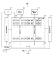
図2は、本技術の第1の実施の形態における固体撮像素子の一構成例を示すブロック図である。この固体撮像素子200は、DAC(Digital to Analog Converter)211と、複数の時刻コード発生部212とを備える。また、固体撮像素子200は、垂直駆動回路213、画素アレイ部220、画素駆動回路214、タイミング生成回路215および出力部250を備える。
図2は、本技術の第1の実施の形態における固体撮像素子の一構成例を示すブロック図である。この固体撮像素子200は、DAC(Digital to Analog Converter)211と、複数の時刻コード発生部212とを備える。また、固体撮像素子200は、垂直駆動回路213、画素アレイ部220、画素駆動回路214、タイミング生成回路215および出力部250を備える。
また、画素アレイ部220は、複数の時刻コード転送部221と、複数の画素230とを備える。時刻コード転送部221は、時刻コード発生部212ごとに配置される。また、複数の画素230は、二次元格子状に配列される。
以下、水平方向に配列された画素230の集合を「行」と称し、行に垂直方向に配列された画素230の集合を「列」と称する。
DAC211は、DA(Digital to Analog)変換により、時間の経過に伴って変化するスロープ状の参照信号を生成するものである。このDAC211は、参照信号を画素アレイ部220に供給する。
時刻コード発生部212は、時刻コードを発生するものである。この時刻コードは、参照信号がスロープ状に変化する期間内の時刻を示す。時刻コード発生部212は、発生した時刻コードを画素アレイ部220に供給する。
タイミング生成回路215は、垂直同期信号VSYNCに同期して様々なタイミング信号を生成し、垂直駆動回路213や出力部250などに供給するものである。
垂直駆動回路213は、タイミング信号に同期して画素230内で生成された画素データを出力部250に出力させる制御を行うものである。画素駆動回路214は、画素230を駆動するものである。
出力部250は、画素データに対して、CDS処理を含む信号処理を実行するものである。この出力部250は、処理後の画素データをデジタルシグナルプロセッサ120に出力する。
時刻コード転送部221は、対応する時刻コード発生部212からの時刻コードを転送するものである。この時刻コード転送部221は、対応する時刻コード発生部212からの時刻コードを画素230へ転送し、また、画素230からの画素データを出力部250に転送する。画素230は、画素データを生成するものである。
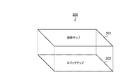
図3は、本技術の第1の実施の形態における固体撮像素子200の積層構造の一例を示す図である。この固体撮像素子200は、画素チップ201と、ロジックチップ202とを備える。固体撮像素子200から光学部110への方向を上方向として、ロジックチップ202の上方に、画素チップ201が積層される。それぞれのチップに設けられる回路については後述する。
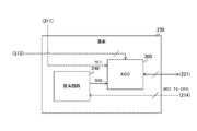
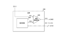
図4は、本技術の第1の実施の形態における画素230の一構成例を示すブロック図である。この画素230は、画素回路240およびADC300を備える。
画素回路240は、画素駆動回路214の制御に従って、受光量に応じたアナログ信号を画素信号SIGとして生成するものである。画素回路240は、画素信号SIGをADC300に供給する。
ADC300は、垂直駆動回路213の制御に従って画素信号SIGをデジタル信号に変換するものである。このADC300は、DAC211からの参照信号REFと画素信号SIGとを比較し、その比較結果VCOに基づいてデジタル信号を生成する。そして、ADC300は、生成したデジタル信号を時刻コード転送部221へ供給する。
[ADCの構成例]
図5は、本技術の第1の実施の形態におけるADC300の一構成例を示すブロック図である。このADC300は、比較回路310およびデータ記憶部350を備える。比較回路310は、差動増幅回路320、電圧変換回路330および正帰還回路340を備える。データ記憶部350は、ラッチ制御部351およびラッチ記憶部352を備える。
図5は、本技術の第1の実施の形態におけるADC300の一構成例を示すブロック図である。このADC300は、比較回路310およびデータ記憶部350を備える。比較回路310は、差動増幅回路320、電圧変換回路330および正帰還回路340を備える。データ記憶部350は、ラッチ制御部351およびラッチ記憶部352を備える。
差動増幅回路320は、DAC211からの参照信号REFと、画素回路240からの画素信号SIGとの差分を増幅するものである。この差動増幅回路320は、差分を増幅した信号を差動増幅信号HVOとして電圧変換回路330に出力する。この差動増幅信号HVOは、例えば、画素信号SIGが参照信号REFより高いときにハイレベルとなる。初期状態において参照信号REFのレベルは最小であり、時間の経過に伴って増大する。このため、差動増幅信号HVOの初期値はハイレベルであり、その後に参照信号REFが画素信号SIG以上になったタイミングで反転してローレベルになる。
電圧変換回路330は、差動増幅信号HVOの電圧を、正帰還回路340が動作可能な低電位に変換し、変換信号LVIとして正帰還回路340に供給するものである。
正帰還回路340は、変換信号LVIに基づいて、参照信号REFが画素信号SIG以上になった際に反転する比較結果VCOをデータ記憶部350に出力するものである。また、正帰還回路340は、垂直駆動回路213からの初期化信号INIにより、初期化される。
ラッチ制御部351は、垂直駆動回路213からの制御信号に従ってラッチ記憶部352の読出し動作と書込み動作とを制御するものである。このラッチ制御部351は、比較結果VCOが反転するまでの間、時刻コード転送部221からの時刻コードをラッチ記憶部352に記憶させる。この時刻コードは、単位時間ごとに更新される。そして、比較結果VCOが反転したときにラッチ制御部351は、時刻コードの更新を中止させ、その時点の時刻コードを保持させる。これにより、差動増幅信号HVOが反転したとき(すなわち、比較結果VCOが反転したとき)までの時間を示すデータ(時刻コード)が画素データとして取得され、ラッチ記憶部352に記憶される。この画素データは、画素230の受光量を表す。
また、参照信号REFの掃引が完了した後に画素データ(時刻コード)の読出し動作が開始される。ラッチ制御部351は、画素230の読出しタイミングにおいてラッチ記憶部352に画素データを出力させる。時刻コード転送部221は、出力された画素データを出力部250に転送する。
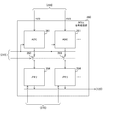
図6は、本技術の第1の実施の形態における画素回路240および差動増幅回路320の一構成例を示す回路図である。画素回路240は、リセットトランジスタ241、転送トランジスタ242、浮遊拡散層243、フォトダイオード244および排出トランジスタ245を備える。例えば、nMOSトランジスタが、リセットトランジスタ241、転送トランジスタ242、フォトダイオード244および排出トランジスタ245として用いられる。なお、差動増幅回路230および画素回路240からなる回路は、特許請求の範囲に記載の半導体集積回路の一例である。
フォトダイオード244は、入射光を光電変換して電荷を生成するものである。排出トランジスタ245は、画素駆動回路214からの排出制御信号OFGに従ってフォトダイオード244の電荷を排出するものである。
転送トランジスタ242は、画素駆動回路214からの転送信号TXに従って、フォトダイオード244から浮遊拡散層243へ電荷を転送するものである。
浮遊拡散層243は、転送された電荷を蓄積し、蓄積した電荷の量に応じた電圧を生成するものである。この電圧の信号が画素信号SIGとして差動増幅回路320へ出力される。
リセットトランジスタ241は、画素駆動回路214からのリセット信号RSTに従って、浮遊拡散層243の電荷量を初期化するものである。
また、差動増幅回路320は、MOSFET321、322および325と、TFET323および324とを備える。MOSFET321および322として、例えば、P型のトランジスタが用いられる。また、TFET323および324と、MOSFET325として、例えば、N型のトランジスタが用いられる。
MOFET321および322は、カレントミラー回路を構成する。MOFET321および322のソースには、電源電圧VDDHが印加される。MOSFET321のドレインは、MOFET321および322のゲートに共通に接続される。MOSFET322のドレインは、電圧変換回路330に接続される。
TFET323および324は、差動対を構成し、これらのトランジスタのソースは、MOSFET325のドレインに共通に接続される。TFET323のドレインは、MOSFET321のドレインに接続され、TFET324のドレインは、MOSFET322のドレインに接続される。また、TFET323のゲートにはDAC211からの参照信号REFが入力され、TFET324のゲートには、画素回路240からの画素信号SIGが入力される。これらの差動対のTFET323および324に入力される参照信号REFと画素信号SIGの差分を増幅した信号が、差動増幅信号HVOとして電圧変換回路330へ出力される。
MOSFET325のゲートには、所定のバイアス電圧Vbが印加され、ソースには、所定の基準電位VSSが印加される。このMOSFET325は、バイアス電圧Vbに応じた定電流を供給する定電流源として機能する。この定電流は、例えば、1乃至100ナノアンペア(nA)に設定される。一般に、ランダムノイズを低減するには、この定電流の値を増やす必要があるが、その代わりに消費電力が増大してしまうおそれがある。
また、画素回路240と、TFET323および324と、MOSFET325とは、画素チップ201に配置される。一方、MOSFET321および322と、その後段の電圧変換回路330、正帰還回路340およびデータ記憶部350などは、ロジックチップ202に配置される。なお、画素チップ201およびロジックチップ202への回路の配置は、図6に例示した構成に限定されない。
図7は、本技術の第1の実施の形態におけるTFETとMOSFETとの電流-電圧特性の一例を示すグラフである。一点鎖線は、MOSFET(MOSFET321など)の特性を示し、実線は、TFET(TFET323など)の特性を示す。同図における縦軸は、ドレイン電流の対数値であり、横軸は、ゲート電圧である。ここで、サブスレッショルド係数Sは、次の式により表される。
S=dVg/d(log10Id) ・・・式1
上式において、Vgは、ゲート電圧であり、単位は、例えば、ボルト(V)である。Idは、ドレイン電流であり、単位は、例えば、アンペア(A)である。
S=dVg/d(log10Id) ・・・式1
上式において、Vgは、ゲート電圧であり、単位は、例えば、ボルト(V)である。Idは、ドレイン電流であり、単位は、例えば、アンペア(A)である。
ドレイン電流が飽和するまでのサブスレッショルド領域において、TFETの曲線の傾きは、MOSFETよりも大きい。したがって、式1より、TFETのサブスレッショルド係数Sは、MOSFETのサブスレッショルド係数よりも小さい。例えば、MOSFETのサブスレッショルド係数Sが、桁当たり70ミリボルト(mV/dec)であるのに対し、TFETのサブスレッショルド係数は、52ミリボルト(mV/dec)程度である。
また、サブスレッショルド領域における出力雑音電流SIdは、次の式により表される。
SId=2qId ・・・式2
上式において、qは、電気素量である。また、式2は、「G. REIMBOLD, et al., White Noise of MOS Transistors Operating in Weak Inversion, IEEE TRANSACTIONS ON ELECTRON DEVICES 1982」に記載されている。
SId=2qId ・・・式2
上式において、qは、電気素量である。また、式2は、「G. REIMBOLD, et al., White Noise of MOS Transistors Operating in Weak Inversion, IEEE TRANSACTIONS ON ELECTRON DEVICES 1982」に記載されている。
次に入力雑音電圧SVgは、次の式により表される。
SVg=SId/gm2 ・・・式3
上式におけるgmは、相互コンダクタンスであり、単位は、例えば、ジーメンス(S)である。
SVg=SId/gm2 ・・・式3
上式におけるgmは、相互コンダクタンスであり、単位は、例えば、ジーメンス(S)である。
式2を式3に代入すると、次の式が得られる。
SVg=(2qId)/gm2 ・・・式4
SVg=(2qId)/gm2 ・・・式4
また、式1を変形すると、次の式が得られる。

式4および式5より、次の式が得られる。
SVg=(2q/Id)・(S/Log10)2
SVg=(2q/Id)・(S/Log10)2
上式より、サブスレッショルド係数Sが小さいほど、熱雑音に応じた入力雑音電圧SVgが小さくなる。そして、前述のように、TFETのサブスレッショルド係数Sは、MOSFETのサブスレッショルド係数よりも小さい。したがって、差動対にTFETを用いた場合、差動増幅信号HVOの熱雑音は、差動対にMOSFETを用いた場合よりも小さくなることがわかる。
このように、差動対にTFETを用いることにより、熱雑音を抑制し、その熱雑音の成分を含むランダムノイズを低減することができる。このため、ランダムノイズ低減を目的として定電流を増大する必要性が低くなり、差動対にMOSFETを用いた場合と比較して、ランダムノイズを許容値未満にする際の定電流の値が小さくて済む。これにより、固体撮像素子200の消費電力を低減することができる。
ただし、同図からも明らかなように、TFETの飽和電流はMOSFETより小さいため、TFETを用いた論理回路では、MOSFETを用いた場合と比較して動作速度が低下するおそれがある。しかしながら、差動増幅回路320は、論理回路ではないため、飽和電流が小さくても問題にならない。
図8は、本技術の第1の実施の形態における画素230内の素子の配置レイアウトの一例を示す図である。以下、受光面に平行な所定方向をX方向とし、受光面に垂直な方向をZ方向とし、X方向およびZ方向に垂直な方向をY方向とする。
フォトダイオード244には、排出トランジスタ245および転送トランジスタ242が接続される。また、リセットトランジスタ241、TFET323、TFET324およびMOSFET325は、X方向に沿って配列される。
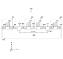
図9は、本技術の第1の実施の形態における画素230の断面図の一例である。同図は、図8のA-A'軸に沿って画素230を切断した場合の断面図である。
基板401に、N型半導体からなるN層402、404、412および414が形成される。N層402および404の間には、ゲート403が形成され、N層412および424の間にはゲート413が形成される。N層402および404にソースおよびドレインが形成され、これらのソースおよびドレインとゲート403とは、リセットトランジスタ241を形成する。また、N層412および414にもソースおよびドレインが形成され、これらのソースおよびドレインとゲート413とは、MOSFET325を形成する。
また、基板401には、n型不純物の濃度が基板401より高いNウェル層415が形成され、Nウェル層415には、N層406および410と、P型半導体からなるP層408とが形成される。P層408は、フォトリソグラフィおよびイオン注入により形成される。N層404および406の間には、素子間分離領域405が設けられる。N層410および412の間にも素子間分離領域411が設けられる。N層406とP層408の間には、ゲート407が形成され、P層408とN層410の間には、ゲート409が形成される。これらのゲートの下部には、P層408の一部が入り込んでおり、その部分は、他の部分より浅く、エクステンションと呼ばれる。
N層406およびP層408にドレインおよびソースが形成され、これらのドレインおよびソースとゲート407とは、TFET324を形成する。また、N層410およびP層408にドレインおよびソースが形成され、これらのドレインおよびソースとゲート409とは、TFET323を形成する。また、これらのTFET323および324のゲート酸化膜は、例えば、3.0乃至6.0ナノメートル(nm)の膜厚に設定され、その周辺のトランジスタ(MOSFET325など)のゲート酸化膜と同時に形成される。
また、TFET323および324のそれぞれのゲート面積は、MOSFET325等の周囲のトランジスタのゲート面積と略同一に設定される。従来(カラムADC)のCMOS(Complementary MOS)イメージセンサにて、例えば解像度より感度を優先する場合など、比較的大面積の画素セルが用いられることがある。この場合、1/fノイズ低減のために大きな面積のゲートを有するアンプトランジスタを画素トランジスタとして適用する場合があり、熱ノイズがランダムノイズを支配する状況になる。アンプトランジスタをサブスレッショルド領域で動作させる場合、本案に従いTFETを適用して熱ノイズを抑制することにより、更なる低ノイズ化が可能になる。
図10は、本技術の第1の実施の形態における電圧変換回路330および正帰還回路340の一構成例を示す回路図である。
電圧変換回路330は、nMOSトランジスタ331を備える。このnMOSトランジスタ331のゲートには電源電圧VDDHより低い電源電圧VDDLが印加される。また、nMOSトランジスタ331のドレインおよびソースは、差動増幅回路320および正帰還回路340に接続される。
正帰還回路340は、pMOSトランジスタ341、342および344と、nMOSトランジスタ343および345とを備える。pMOSトランジスタ341および342とnMOSトランジスタ343とは、電源電圧VDDLに直列に接続される。また、pMOSトランジスタ344およびnMOSトランジスタ345は、電源電圧VDDLに直列に接続される。
また、pMOSトランジスタ341およびnMOSトランジスタ343のゲートには、垂直駆動回路213からの初期化信号INIが入力される。pMOSトランジスタ342のゲートは、pMOSトランジスタ344およびnMOSトランジスタ345の接続点に接続される。また、pMOSトランジスタ344およびnMOSトランジスタ345のゲートは、電圧変換回路330と、pMOSトランジスタ342およびnMOSトランジスタ343の接続点とに共通に接続される。pMOSトランジスタ344およびnMOSトランジスタ345の接続点の電位は、比較結果VCOとして、データ記憶部350に出力される。
なお、電圧変換回路330および正帰還回路340のそれぞれは、図5で説明した機能を持つのであれば、図10に例示した回路に限定されない。
このように、本技術の第1の実施の形態によれば、画素信号SIGと参照信号REFとの差を増幅する差動対としてTFET323および324を用いたため、MOSFETを用いる場合と比較して、熱雑音を抑制することができる。これにより、熱雑音の成分を含む雑音を低減することができる。
<2.第2の実施の形態>
上述の第1の実施の形態では、画素ごとにADC300を配置していたが、画素数の増大に伴ってADC300の個数が増大し、画素アレイ部220の回路規模が大きくなるという問題がある。この第2の実施の形態の固体撮像素子200は、列ごとにADCを配置した点において第1の実施の形態と異なる。
上述の第1の実施の形態では、画素ごとにADC300を配置していたが、画素数の増大に伴ってADC300の個数が増大し、画素アレイ部220の回路規模が大きくなるという問題がある。この第2の実施の形態の固体撮像素子200は、列ごとにADCを配置した点において第1の実施の形態と異なる。
図11は、本技術の第2の実施の形態における固体撮像素子200の一構成例を示すブロック図である。この固体撮像素子200は、DAC211、垂直駆動回路213、タイミング生成回路215、画素アレイ部220、カラム信号処理部260および水平走査回路270を備える。画素アレイ部220には、二次元格子状に複数の画素230が配列される。
第2の実施の形態の垂直駆動回路213は、行を順に選択して駆動する。第2の実施の形態のDAC211およびタイミング生成回路215の構成は、第1の実施の形態と同様である。
第2の実施の形態の画素230は、差動増幅信号HVOをカラム信号処理部260に供給する。
カラム信号処理部260は、列のそれぞれからの差動増幅信号HVOをAD(Analog to Digital)変換して画素データとして保持するものである。水平走査回路270は、列を順に選択して、その列の画素データをデジタルシグナルプロセッサ120に出力させるものである。
図12は、本技術の第2の実施の形態における画素230の一構成例を示すブロック図である。第2の実施の形態の画素230は、画素回路240および差動増幅回路320を備える。
第2の実施の形態の画素回路240は、垂直駆動回路213の制御に従って画素信号SIGを生成し、差動増幅回路320に供給する。第2の実施の形態の差動増幅回路320は、画素信号SIGと参照信号REFとの差分を増幅して差動増幅信号HVOとして、カラム信号処理部260へ供給する。
図13は、本技術の第2の実施の形態におけるカラム信号処理部260の一構成例を示すブロック図である。カラム信号処理部260は、列ごとにADC261、スイッチ263およびメモリ264を備える。
ADC261は、タイミング生成回路215の制御に従って、対応する列からの差動増幅信号HVOをデジタルの画素データに変換するものである。スイッチ263は、タイミング生成回路215の制御に従って、ADC261からの画素データをメモリ264に記憶させるものである。
メモリ264は、画素データを記憶するものである。このメモリ264は、水平走査回路270の制御に従って、画素データをデジタルシグナルプロセッサ120に出力する。なお、メモリ264は、特許請求の範囲に記載のデータ記憶部の一例である。
図14は、本技術の第2の実施の形態におけるADC261の一構成例を示すブロック図である。このADC261は、電圧変換回路330、正帰還回路340およびカウンタ262を備える。第2の実施の形態の電圧変換回路330および正帰還回路340の構成は、第1の実施の形態と同様である。正帰還回路340は、比較結果VCOをカウンタ262に供給する。
カウンタ262は、タイミング生成回路215の制御に従って、比較結果VCOが反転するまでの期間に亘って、タイミング生成回路215からのクロック信号に同期して計数値を計数するものである。この計数値は、比較結果VCOが反転するまでの時間を示す。カウンタ262は、計数値を示すデータを画素データとしてスイッチ263に供給する。
このように、本技術の第2の実施の形態では、列ごとにADC261を配置したため、画素ごとにADCを配置する第1の実施の形態と比較して画素アレイ部220の回路規模を削減することができる。
<移動体への応用例>
本開示に係る技術(本技術)は、様々な製品へ応用することができる。例えば、本開示に係る技術は、自動車、電気自動車、ハイブリッド電気自動車、自動二輪車、自転車、パーソナルモビリティ、飛行機、ドローン、船舶、ロボット等のいずれかの種類の移動体に搭載される装置として実現されてもよい。
本開示に係る技術(本技術)は、様々な製品へ応用することができる。例えば、本開示に係る技術は、自動車、電気自動車、ハイブリッド電気自動車、自動二輪車、自転車、パーソナルモビリティ、飛行機、ドローン、船舶、ロボット等のいずれかの種類の移動体に搭載される装置として実現されてもよい。
図15は、本開示に係る技術が適用され得る移動体制御システムの一例である車両制御システムの概略的な構成例を示すブロック図である。
車両制御システム12000は、通信ネットワーク12001を介して接続された複数の電子制御ユニットを備える。図15に示した例では、車両制御システム12000は、駆動系制御ユニット12010、ボディ系制御ユニット12020、車外情報検出ユニット12030、車内情報検出ユニット12040、及び統合制御ユニット12050を備える。また、統合制御ユニット12050の機能構成として、マイクロコンピュータ12051、音声画像出力部12052、及び車載ネットワークI/F(interface)12053が図示されている。
駆動系制御ユニット12010は、各種プログラムにしたがって車両の駆動系に関連する装置の動作を制御する。例えば、駆動系制御ユニット12010は、内燃機関又は駆動用モータ等の車両の駆動力を発生させるための駆動力発生装置、駆動力を車輪に伝達するための駆動力伝達機構、車両の舵角を調節するステアリング機構、及び、車両の制動力を発生させる制動装置等の制御装置として機能する。
ボディ系制御ユニット12020は、各種プログラムにしたがって車体に装備された各種装置の動作を制御する。例えば、ボディ系制御ユニット12020は、キーレスエントリシステム、スマートキーシステム、パワーウィンドウ装置、あるいは、ヘッドランプ、バックランプ、ブレーキランプ、ウィンカー又はフォグランプ等の各種ランプの制御装置として機能する。この場合、ボディ系制御ユニット12020には、鍵を代替する携帯機から発信される電波又は各種スイッチの信号が入力され得る。ボディ系制御ユニット12020は、これらの電波又は信号の入力を受け付け、車両のドアロック装置、パワーウィンドウ装置、ランプ等を制御する。
車外情報検出ユニット12030は、車両制御システム12000を搭載した車両の外部の情報を検出する。例えば、車外情報検出ユニット12030には、撮像部12031が接続される。車外情報検出ユニット12030は、撮像部12031に車外の画像を撮像させるとともに、撮像された画像を受信する。車外情報検出ユニット12030は、受信した画像に基づいて、人、車、障害物、標識又は路面上の文字等の物体検出処理又は距離検出処理を行ってもよい。
撮像部12031は、光を受光し、その光の受光量に応じた電気信号を出力する光センサである。撮像部12031は、電気信号を画像として出力することもできるし、測距の情報として出力することもできる。また、撮像部12031が受光する光は、可視光であっても良いし、赤外線等の非可視光であっても良い。
車内情報検出ユニット12040は、車内の情報を検出する。車内情報検出ユニット12040には、例えば、運転者の状態を検出する運転者状態検出部12041が接続される。運転者状態検出部12041は、例えば運転者を撮像するカメラを含み、車内情報検出ユニット12040は、運転者状態検出部12041から入力される検出情報に基づいて、運転者の疲労度合い又は集中度合いを算出してもよいし、運転者が居眠りをしていないかを判別してもよい。
マイクロコンピュータ12051は、車外情報検出ユニット12030又は車内情報検出ユニット12040で取得される車内外の情報に基づいて、駆動力発生装置、ステアリング機構又は制動装置の制御目標値を演算し、駆動系制御ユニット12010に対して制御指令を出力することができる。例えば、マイクロコンピュータ12051は、車両の衝突回避あるいは衝撃緩和、車間距離に基づく追従走行、車速維持走行、車両の衝突警告、又は車両のレーン逸脱警告等を含むADAS(Advanced Driver Assistance System)の機能実現を目的とした協調制御を行うことができる。
また、マイクロコンピュータ12051は、車外情報検出ユニット12030又は車内情報検出ユニット12040で取得される車両の周囲の情報に基づいて駆動力発生装置、ステアリング機構又は制動装置等を制御することにより、運転者の操作に拠らずに自律的に走行する自動運転等を目的とした協調制御を行うことができる。
また、マイクロコンピュータ12051は、車外情報検出ユニット12030で取得される車外の情報に基づいて、ボディ系制御ユニット12020に対して制御指令を出力することができる。例えば、マイクロコンピュータ12051は、車外情報検出ユニット12030で検知した先行車又は対向車の位置に応じてヘッドランプを制御し、ハイビームをロービームに切り替える等の防眩を図ることを目的とした協調制御を行うことができる。
音声画像出力部12052は、車両の搭乗者又は車外に対して、視覚的又は聴覚的に情報を通知することが可能な出力装置へ音声及び画像のうちの少なくとも一方の出力信号を送信する。図15の例では、出力装置として、オーディオスピーカ12061、表示部12062及びインストルメントパネル12063が例示されている。表示部12062は、例えば、オンボードディスプレイ及びヘッドアップディスプレイの少なくとも一つを含んでいてもよい。
図16は、撮像部12031の設置位置の例を示す図である。
図16では、撮像部12031として、撮像部12101,12102,12103,12104,12105を有する。
撮像部12101,12102,12103,12104,12105は、例えば、車両12100のフロントノーズ、サイドミラー、リアバンパ、バックドア及び車室内のフロントガラスの上部等の位置に設けられる。フロントノーズに備えられる撮像部12101及び車室内のフロントガラスの上部に備えられる撮像部12105は、主として車両12100の前方の画像を取得する。サイドミラーに備えられる撮像部12102,12103は、主として車両12100の側方の画像を取得する。リアバンパ又はバックドアに備えられる撮像部12104は、主として車両12100の後方の画像を取得する。車室内のフロントガラスの上部に備えられる撮像部12105は、主として先行車両又は、歩行者、障害物、信号機、交通標識又は車線等の検出に用いられる。
なお、図16には、撮像部12101ないし12104の撮影範囲の一例が示されている。撮像範囲12111は、フロントノーズに設けられた撮像部12101の撮像範囲を示し、撮像範囲12112,12113は、それぞれサイドミラーに設けられた撮像部12102,12103の撮像範囲を示し、撮像範囲12114は、リアバンパ又はバックドアに設けられた撮像部12104の撮像範囲を示す。例えば、撮像部12101ないし12104で撮像された画像データが重ね合わせられることにより、車両12100を上方から見た俯瞰画像が得られる。
撮像部12101ないし12104の少なくとも1つは、距離情報を取得する機能を有していてもよい。例えば、撮像部12101ないし12104の少なくとも1つは、複数の撮像素子からなるステレオカメラであってもよいし、位相差検出用の画素を有する撮像素子であってもよい。
例えば、マイクロコンピュータ12051は、撮像部12101ないし12104から得られた距離情報を基に、撮像範囲12111ないし12114内における各立体物までの距離と、この距離の時間的変化(車両12100に対する相対速度)を求めることにより、特に車両12100の進行路上にある最も近い立体物で、車両12100と略同じ方向に所定の速度(例えば、0km/h以上)で走行する立体物を先行車として抽出することができる。さらに、マイクロコンピュータ12051は、先行車の手前に予め確保すべき車間距離を設定し、自動ブレーキ制御(追従停止制御も含む)や自動加速制御(追従発進制御も含む)等を行うことができる。このように運転者の操作に拠らずに自律的に走行する自動運転等を目的とした協調制御を行うことができる。
例えば、マイクロコンピュータ12051は、撮像部12101ないし12104から得られた距離情報を元に、立体物に関する立体物データを、2輪車、普通車両、大型車両、歩行者、電柱等その他の立体物に分類して抽出し、障害物の自動回避に用いることができる。例えば、マイクロコンピュータ12051は、車両12100の周辺の障害物を、車両12100のドライバが視認可能な障害物と視認困難な障害物とに識別する。そして、マイクロコンピュータ12051は、各障害物との衝突の危険度を示す衝突リスクを判断し、衝突リスクが設定値以上で衝突可能性がある状況であるときには、オーディオスピーカ12061や表示部12062を介してドライバに警報を出力することや、駆動系制御ユニット12010を介して強制減速や回避操舵を行うことで、衝突回避のための運転支援を行うことができる。
撮像部12101ないし12104の少なくとも1つは、赤外線を検出する赤外線カメラであってもよい。例えば、マイクロコンピュータ12051は、撮像部12101ないし12104の撮像画像中に歩行者が存在するか否かを判定することで歩行者を認識することができる。かかる歩行者の認識は、例えば赤外線カメラとしての撮像部12101ないし12104の撮像画像における特徴点を抽出する手順と、物体の輪郭を示す一連の特徴点にパターンマッチング処理を行って歩行者か否かを判別する手順によって行われる。マイクロコンピュータ12051が、撮像部12101ないし12104の撮像画像中に歩行者が存在すると判定し、歩行者を認識すると、音声画像出力部12052は、当該認識された歩行者に強調のための方形輪郭線を重畳表示するように、表示部12062を制御する。また、音声画像出力部12052は、歩行者を示すアイコン等を所望の位置に表示するように表示部12062を制御してもよい。
以上、本開示に係る技術が適用され得る車両制御システムの一例について説明した。本開示に係る技術は、以上説明した構成のうち、撮像部12031に適用され得る。具体的には、図1の撮像装置100を、撮像部12031に適用することができる。撮像部12031に本開示に係る技術を適用することにより、熱雑音を低減して、より見やすい撮影画像を得ることができるため、ドライバの疲労を軽減することが可能になる。
なお、上述の実施の形態は本技術を具現化するための一例を示したものであり、実施の形態における事項と、特許請求の範囲における発明特定事項とはそれぞれ対応関係を有する。同様に、特許請求の範囲における発明特定事項と、これと同一名称を付した本技術の実施の形態における事項とはそれぞれ対応関係を有する。ただし、本技術は実施の形態に限定されるものではなく、その要旨を逸脱しない範囲において実施の形態に種々の変形を施すことにより具現化することができる。
なお、本明細書に記載された効果はあくまで例示であって、限定されるものではなく、また、他の効果があってもよい。
なお、本技術は以下のような構成もとることができる。
(1)入射光を光電変換して画素信号を生成する画素回路と、
前記画素信号と時間の経過に伴って変化する所定の参照信号との差を増幅して差動増幅信号として出力する一対のTFET(Tunnel Field Effect Transistor)と
を具備する半導体集積回路。
(2)前記一対のTFETに一定の電流を供給するMOSFET(Metal Oxide Semiconductor Field Effect Transistor)をさらに具備し、
前記MOSFETのゲートの面積は、前記一対のTFETのそれぞれのゲート面積と略同一である
前記(1)記載の半導体集積回路。
(3)前記画素回路は、二次元格子状に所定数配列され、
前記一対のTFETは、前記画素回路ごとに設けられる
前記(1)または(2)に記載の半導体集積回路。
(4)前記差動増幅信号が初期値と異なる値に変化するまでの時間を示すデータを画素データとして取得して記憶するデータ記憶部をさらに具備する
前記(1)記載の半導体集積回路。
(5)前記データ記憶部は、前記画素回路ごとに設けられる
前記(4)記載の半導体集積回路。
(6)前記記憶部は、所定方向に配列された前記画素回路の集合である列ごとに設けられる
前記(4)記載の半導体集積回路。
(7)基板と、
前記基板に形成されたNウェル層と、
N型半導体からなる一対のN層と、
P型半導体からなるP層と
をさらに具備し、
前記P層と前記一対のN層とは、前記Nウェル層に設けられ、
前記P層は、前記Nウェル層において前記一対のN層の間に配置され、
前記一対のTFETのそれぞれのソースは、前記P層に形成され、
前記一対のTFETのそれぞれのドレインは、前記一対のN層のそれぞれに形成される
前(1)から(6)のいずれかに記載の半導体集積回路。(8)入射光を光電変換して画素信号を生成する画素回路と、
前記画素信号と時間の経過に伴って変化する所定の参照信号との差を増幅して差動増幅信号として出力する一対のTFET(Tunnel Field Effect Transistor)と、
前記差動増幅信号が初期値と異なる値に変化するまでの時間を示すデータを画素データとして取得して記憶するデータ記憶部と、
前記画素データに対して所定の処理を実行する処理部と
を具備する撮像装置。
(1)入射光を光電変換して画素信号を生成する画素回路と、
前記画素信号と時間の経過に伴って変化する所定の参照信号との差を増幅して差動増幅信号として出力する一対のTFET(Tunnel Field Effect Transistor)と
を具備する半導体集積回路。
(2)前記一対のTFETに一定の電流を供給するMOSFET(Metal Oxide Semiconductor Field Effect Transistor)をさらに具備し、
前記MOSFETのゲートの面積は、前記一対のTFETのそれぞれのゲート面積と略同一である
前記(1)記載の半導体集積回路。
(3)前記画素回路は、二次元格子状に所定数配列され、
前記一対のTFETは、前記画素回路ごとに設けられる
前記(1)または(2)に記載の半導体集積回路。
(4)前記差動増幅信号が初期値と異なる値に変化するまでの時間を示すデータを画素データとして取得して記憶するデータ記憶部をさらに具備する
前記(1)記載の半導体集積回路。
(5)前記データ記憶部は、前記画素回路ごとに設けられる
前記(4)記載の半導体集積回路。
(6)前記記憶部は、所定方向に配列された前記画素回路の集合である列ごとに設けられる
前記(4)記載の半導体集積回路。
(7)基板と、
前記基板に形成されたNウェル層と、
N型半導体からなる一対のN層と、
P型半導体からなるP層と
をさらに具備し、
前記P層と前記一対のN層とは、前記Nウェル層に設けられ、
前記P層は、前記Nウェル層において前記一対のN層の間に配置され、
前記一対のTFETのそれぞれのソースは、前記P層に形成され、
前記一対のTFETのそれぞれのドレインは、前記一対のN層のそれぞれに形成される
前(1)から(6)のいずれかに記載の半導体集積回路。(8)入射光を光電変換して画素信号を生成する画素回路と、
前記画素信号と時間の経過に伴って変化する所定の参照信号との差を増幅して差動増幅信号として出力する一対のTFET(Tunnel Field Effect Transistor)と、
前記差動増幅信号が初期値と異なる値に変化するまでの時間を示すデータを画素データとして取得して記憶するデータ記憶部と、
前記画素データに対して所定の処理を実行する処理部と
を具備する撮像装置。
100 撮像装置
110 光学部
120 デジタルシグナルプロセッサ
130 表示部
140 操作部
150 バス
160 フレームメモリ
170 記録部
180 電源部
200 固体撮像素子
201 画素チップ
202 ロジックチップ
211 DAC
212 時刻コード発生部
213 垂直駆動回路
214 画素駆動回路
215 タイミング生成回路
220 画素アレイ部
221 時刻コード転送部
230 画素
240 画素回路
241 リセットトランジスタ
242 転送トランジスタ
243 浮遊拡散層
244 フォトダイオード
245 排出トランジスタ
250 出力部
260 カラム信号処理部
261、300 ADC
262 カウンタ
263 スイッチ
264 メモリ
270 水平走査回路
310 比較回路
320 差動増幅回路
321、322、325 MOSFET
323、324 TFET
330 電圧変換回路
331、343、345 nMOSトランジスタ
340 正帰還回路
341、342、344 pMOSトランジスタ
350 データ記憶部
351 ラッチ制御部
352 ラッチ記憶部
12031 撮像部
110 光学部
120 デジタルシグナルプロセッサ
130 表示部
140 操作部
150 バス
160 フレームメモリ
170 記録部
180 電源部
200 固体撮像素子
201 画素チップ
202 ロジックチップ
211 DAC
212 時刻コード発生部
213 垂直駆動回路
214 画素駆動回路
215 タイミング生成回路
220 画素アレイ部
221 時刻コード転送部
230 画素
240 画素回路
241 リセットトランジスタ
242 転送トランジスタ
243 浮遊拡散層
244 フォトダイオード
245 排出トランジスタ
250 出力部
260 カラム信号処理部
261、300 ADC
262 カウンタ
263 スイッチ
264 メモリ
270 水平走査回路
310 比較回路
320 差動増幅回路
321、322、325 MOSFET
323、324 TFET
330 電圧変換回路
331、343、345 nMOSトランジスタ
340 正帰還回路
341、342、344 pMOSトランジスタ
350 データ記憶部
351 ラッチ制御部
352 ラッチ記憶部
12031 撮像部
Claims (8)
- 入射光を光電変換して画素信号を生成する画素回路と、
前記画素信号と時間の経過に伴って変化する所定の参照信号との差を増幅して差動増幅信号として出力する一対のTFET(Tunnel Field Effect Transistor)と
を具備する半導体集積回路。 - 前記一対のTFETに一定の電流を供給するMOSFET(Metal Oxide Semiconductor Field Effect Transistor)をさらに具備し、
前記MOSFETのゲートの面積は、前記一対のTFETのそれぞれのゲート面積と略同一である
請求項1記載の半導体集積回路。 - 前記画素回路は、二次元格子状に所定数配列され、
前記一対のTFETは、前記画素回路ごとに設けられる
請求項1記載の半導体集積回路。 - 前記差動増幅信号が初期値と異なる値に変化するまでの時間を示すデータを画素データとして取得して記憶するデータ記憶部をさらに具備する
請求項1記載の半導体集積回路。 - 前記データ記憶部は、前記画素回路ごとに設けられる
請求項4記載の半導体集積回路。 - 前記記憶部は、所定方向に配列された前記画素回路の集合である列ごとに設けられる
請求項4記載の半導体集積回路。 - 基板と、
前記基板に形成されたNウェル層と、
N型半導体からなる一対のN層と、
P型半導体からなるP層と
をさらに具備し、
前記P層と前記一対のN層とは、前記Nウェル層に設けられ、
前記P層は、前記Nウェル層において前記一対のN層の間に配置され、
前記一対のTFETのそれぞれのソースは、前記P層に形成され、
前記一対のTFETのそれぞれのドレインは、前記一対のN層のそれぞれに形成される
請求項1記載の半導体集積回路。 - 入射光を光電変換して画素信号を生成する画素回路と、
前記画素信号と時間の経過に伴って変化する所定の参照信号との差を増幅して差動増幅信号として出力する一対のTFET(Tunnel Field Effect Transistor)と、
前記差動増幅信号が初期値と異なる値に変化するまでの時間を示す時間情報を画素データとして取得して記憶するデータ記憶部と、
前記画素データに対して所定の処理を実行する処理部と
を具備する撮像装置。
Priority Applications (1)
| Application Number | Priority Date | Filing Date | Title |
|---|---|---|---|
| US16/761,464 US11350050B2 (en) | 2017-11-13 | 2018-09-25 | Semiconductor integrated circuit and imaging device |
Applications Claiming Priority (2)
| Application Number | Priority Date | Filing Date | Title |
|---|---|---|---|
| JP2017217865 | 2017-11-13 | ||
| JP2017-217865 | 2017-11-13 |
Publications (1)
| Publication Number | Publication Date |
|---|---|
| WO2019092999A1 true WO2019092999A1 (ja) | 2019-05-16 |
Family
ID=66437653
Family Applications (1)
| Application Number | Title | Priority Date | Filing Date |
|---|---|---|---|
| PCT/JP2018/035401 Ceased WO2019092999A1 (ja) | 2017-11-13 | 2018-09-25 | 半導体集積回路、および、撮像装置 |
Country Status (2)
| Country | Link |
|---|---|
| US (1) | US11350050B2 (ja) |
| WO (1) | WO2019092999A1 (ja) |
Cited By (1)
| Publication number | Priority date | Publication date | Assignee | Title |
|---|---|---|---|---|
| WO2023026525A1 (ja) * | 2021-08-24 | 2023-03-02 | ソニーセミコンダクタソリューションズ株式会社 | 情報処理装置 |
Families Citing this family (3)
| Publication number | Priority date | Publication date | Assignee | Title |
|---|---|---|---|---|
| US11368639B2 (en) * | 2019-09-30 | 2022-06-21 | Canon Kabushiki Kaisha | Photoelectric conversion apparatus, image capturing system, method for driving photoelectric conversion apparatus, and moving object |
| DE102022100707B4 (de) | 2021-06-09 | 2026-03-26 | Taiwan Semiconductor Manufacturing Company, Ltd. | Gemeinsam verwendete wannenstruktur, layout und verfahren |
| CN115224028A (zh) * | 2021-06-09 | 2022-10-21 | 台湾积体电路制造股份有限公司 | 共用阱结构、布局和方法 |
Citations (3)
| Publication number | Priority date | Publication date | Assignee | Title |
|---|---|---|---|---|
| JP2013069977A (ja) * | 2011-09-26 | 2013-04-18 | Toshiba Corp | 半導体装置の製造方法 |
| WO2016042876A1 (ja) * | 2014-09-19 | 2016-03-24 | 株式会社 東芝 | 半導体集積回路 |
| WO2016136448A1 (ja) * | 2015-02-23 | 2016-09-01 | ソニー株式会社 | 比較器、ad変換器、固体撮像装置、電子機器、比較器の制御方法、データ書込回路、データ読出回路、およびデータ転送回路 |
Family Cites Families (3)
| Publication number | Priority date | Publication date | Assignee | Title |
|---|---|---|---|---|
| JP4676885B2 (ja) * | 2006-01-04 | 2011-04-27 | 富士通セミコンダクター株式会社 | バイアス回路 |
| TWI659652B (zh) * | 2013-08-05 | 2019-05-11 | 新力股份有限公司 | 攝像裝置、電子機器 |
| US9800094B2 (en) * | 2014-05-14 | 2017-10-24 | The Penn State Research Foundation | Low power nanoelectronics |
-
2018
- 2018-09-25 WO PCT/JP2018/035401 patent/WO2019092999A1/ja not_active Ceased
- 2018-09-25 US US16/761,464 patent/US11350050B2/en active Active
Patent Citations (3)
| Publication number | Priority date | Publication date | Assignee | Title |
|---|---|---|---|---|
| JP2013069977A (ja) * | 2011-09-26 | 2013-04-18 | Toshiba Corp | 半導体装置の製造方法 |
| WO2016042876A1 (ja) * | 2014-09-19 | 2016-03-24 | 株式会社 東芝 | 半導体集積回路 |
| WO2016136448A1 (ja) * | 2015-02-23 | 2016-09-01 | ソニー株式会社 | 比較器、ad変換器、固体撮像装置、電子機器、比較器の制御方法、データ書込回路、データ読出回路、およびデータ転送回路 |
Non-Patent Citations (3)
| Title |
|---|
| KIM ET AL.: "A Steep-Slope Tunnel FET Based SAR Analog-to-Digital Converter", IEEE TRANSACTIONS ON ELECTRON DEVICES, vol. 61, no. 11, 14 October 2014 (2014-10-14), pages 3661 - 7, XP011562014, DOI: doi:10.1109/TED.2014.2359663 * |
| MARTINO ET AL.: "Analysis of TFET and FinFET Differential Pairs with Active Load from 300K to 450K", 2016 JOINT INTERNATIONAL EUROSOI WORKSHOP AND INTERNATIONAL CONFERENCE ON ULTIMATE INTEGRATION ON SILICON (EUROSOI-ULIS, 24 March 2016 (2016-03-24), pages 246 - 249, XP032885696 * |
| SEDIGHI ET AL.: "Analog Circuit Design Using Tunnel-FETs", IEEE TRANSACTIONS ON CIRCUITS AND SYSTEMS-1: REGULAR PAPERS, vol. 62, no. 1, 12 August 2014 (2014-08-12), pages 39 - 48, XP011569519, DOI: doi:10.1109/TCSI.2014.2342371 * |
Cited By (1)
| Publication number | Priority date | Publication date | Assignee | Title |
|---|---|---|---|---|
| WO2023026525A1 (ja) * | 2021-08-24 | 2023-03-02 | ソニーセミコンダクタソリューションズ株式会社 | 情報処理装置 |
Also Published As
| Publication number | Publication date |
|---|---|
| US11350050B2 (en) | 2022-05-31 |
| US20200396408A1 (en) | 2020-12-17 |
Similar Documents
| Publication | Publication Date | Title |
|---|---|---|
| US11659304B2 (en) | Solid-state imaging element, imaging device, and control method of solid-state imaging element | |
| US12185009B2 (en) | Image sensor, method of controlling image sensor, and electronic device | |
| US11582416B2 (en) | Solid-state image sensor, imaging device, and method of controlling solid-state image sensor | |
| US11950009B2 (en) | Solid-state image sensor | |
| JP7148269B2 (ja) | 固体撮像素子および撮像装置 | |
| US11265503B2 (en) | Analog to digital converter, solid-state imaging element, and control method of analog to digital converter | |
| US12219282B2 (en) | Image sensor, method of controlling image sensor, and electronic device | |
| US11252367B2 (en) | Solid-stage image sensor, imaging device, and method of controlling solid-state image sensor | |
| WO2021256095A1 (ja) | 撮像装置及び撮像方法 | |
| US12302023B2 (en) | Solid-state imaging element and imaging device that detect address event | |
| US11350050B2 (en) | Semiconductor integrated circuit and imaging device | |
| JP2021170691A (ja) | 撮像素子、制御方法、および電子機器 | |
| US11381764B2 (en) | Sensor element and electronic device | |
| US12267609B2 (en) | Solid-state imaging device | |
| JP2023030996A (ja) | 情報処理装置 | |
| JP2022144106A (ja) | イベント検出素子及び電子機器 | |
| US12294800B2 (en) | Solid-state imaging element | |
| US20240205557A1 (en) | Imaging device, electronic apparatus, and imaging method | |
| WO2022153746A1 (ja) | 撮像装置 | |
| JP2022141460A (ja) | 固体撮像素子及び撮像装置 | |
| US12133008B2 (en) | Solid-state imaging element and imaging device | |
| US20250227390A1 (en) | Linear sensor | |
| WO2023058345A1 (ja) | 撮像装置 | |
| TW202341722A (zh) | 比較器、放大器及固態攝像裝置 | |
| WO2024034352A1 (ja) | 光検出素子、電子機器、及び、光検出素子の製造方法 |
Legal Events
| Date | Code | Title | Description |
|---|---|---|---|
| 121 | Ep: the epo has been informed by wipo that ep was designated in this application |
Ref document number: 18875999 Country of ref document: EP Kind code of ref document: A1 |
|
| NENP | Non-entry into the national phase |
Ref country code: DE |
|
| 122 | Ep: pct application non-entry in european phase |
Ref document number: 18875999 Country of ref document: EP Kind code of ref document: A1 |
|
| NENP | Non-entry into the national phase |
Ref country code: JP |