WO2019064591A1 - Dispositif d'affichage et procédé de fabrication de dispositif d'affichage - Google Patents
Dispositif d'affichage et procédé de fabrication de dispositif d'affichage Download PDFInfo
- Publication number
- WO2019064591A1 WO2019064591A1 PCT/JP2017/035729 JP2017035729W WO2019064591A1 WO 2019064591 A1 WO2019064591 A1 WO 2019064591A1 JP 2017035729 W JP2017035729 W JP 2017035729W WO 2019064591 A1 WO2019064591 A1 WO 2019064591A1
- Authority
- WO
- WIPO (PCT)
- Prior art keywords
- film
- inorganic sealing
- sealing film
- display device
- organic
- Prior art date
Links
- 238000004519 manufacturing process Methods 0.000 title claims description 26
- 238000000034 method Methods 0.000 title claims description 10
- 238000007789 sealing Methods 0.000 claims abstract description 125
- 229910052581 Si3N4 Inorganic materials 0.000 claims description 19
- HQVNEWCFYHHQES-UHFFFAOYSA-N silicon nitride Chemical compound N12[Si]34N5[Si]62N3[Si]51N64 HQVNEWCFYHHQES-UHFFFAOYSA-N 0.000 claims description 19
- XUIMIQQOPSSXEZ-UHFFFAOYSA-N Silicon Chemical compound [Si] XUIMIQQOPSSXEZ-UHFFFAOYSA-N 0.000 claims description 17
- 239000010703 silicon Substances 0.000 claims description 17
- 229910052710 silicon Inorganic materials 0.000 claims description 17
- QVGXLLKOCUKJST-UHFFFAOYSA-N atomic oxygen Chemical compound [O] QVGXLLKOCUKJST-UHFFFAOYSA-N 0.000 claims description 10
- 229910052760 oxygen Inorganic materials 0.000 claims description 10
- 239000001301 oxygen Substances 0.000 claims description 10
- 230000003014 reinforcing effect Effects 0.000 claims description 8
- 230000015572 biosynthetic process Effects 0.000 claims description 4
- 238000005520 cutting process Methods 0.000 claims description 2
- 230000002093 peripheral effect Effects 0.000 abstract 1
- 239000010408 film Substances 0.000 description 244
- 239000010410 layer Substances 0.000 description 100
- VYPSYNLAJGMNEJ-UHFFFAOYSA-N Silicium dioxide Chemical compound O=[Si]=O VYPSYNLAJGMNEJ-UHFFFAOYSA-N 0.000 description 17
- 229910052814 silicon oxide Inorganic materials 0.000 description 17
- NIXOWILDQLNWCW-UHFFFAOYSA-N acrylic acid group Chemical group C(C=C)(=O)O NIXOWILDQLNWCW-UHFFFAOYSA-N 0.000 description 12
- 238000005401 electroluminescence Methods 0.000 description 11
- 239000011347 resin Substances 0.000 description 11
- 229920005989 resin Polymers 0.000 description 11
- 230000004888 barrier function Effects 0.000 description 7
- 239000004065 semiconductor Substances 0.000 description 7
- 239000000758 substrate Substances 0.000 description 7
- 230000000149 penetrating effect Effects 0.000 description 6
- 239000004642 Polyimide Substances 0.000 description 5
- 229920001721 polyimide Polymers 0.000 description 5
- 238000002347 injection Methods 0.000 description 4
- 239000007924 injection Substances 0.000 description 4
- 239000011368 organic material Substances 0.000 description 4
- 238000005452 bending Methods 0.000 description 3
- 238000005229 chemical vapour deposition Methods 0.000 description 3
- 239000000463 material Substances 0.000 description 3
- 229920000139 polyethylene terephthalate Polymers 0.000 description 3
- 239000005020 polyethylene terephthalate Substances 0.000 description 3
- 229910045601 alloy Inorganic materials 0.000 description 2
- 239000000956 alloy Substances 0.000 description 2
- 239000011651 chromium Substances 0.000 description 2
- 239000010949 copper Substances 0.000 description 2
- 239000013039 cover film Substances 0.000 description 2
- 238000010586 diagram Methods 0.000 description 2
- 230000005525 hole transport Effects 0.000 description 2
- AMGQUBHHOARCQH-UHFFFAOYSA-N indium;oxotin Chemical compound [In].[Sn]=O AMGQUBHHOARCQH-UHFFFAOYSA-N 0.000 description 2
- 238000010030 laminating Methods 0.000 description 2
- 230000004048 modification Effects 0.000 description 2
- 238000012986 modification Methods 0.000 description 2
- 239000002096 quantum dot Substances 0.000 description 2
- 239000010409 thin film Substances 0.000 description 2
- 239000010936 titanium Substances 0.000 description 2
- XLYOFNOQVPJJNP-UHFFFAOYSA-N water Substances O XLYOFNOQVPJJNP-UHFFFAOYSA-N 0.000 description 2
- VYZAMTAEIAYCRO-UHFFFAOYSA-N Chromium Chemical compound [Cr] VYZAMTAEIAYCRO-UHFFFAOYSA-N 0.000 description 1
- RYGMFSIKBFXOCR-UHFFFAOYSA-N Copper Chemical compound [Cu] RYGMFSIKBFXOCR-UHFFFAOYSA-N 0.000 description 1
- ZOKXTWBITQBERF-UHFFFAOYSA-N Molybdenum Chemical compound [Mo] ZOKXTWBITQBERF-UHFFFAOYSA-N 0.000 description 1
- RTAQQCXQSZGOHL-UHFFFAOYSA-N Titanium Chemical compound [Ti] RTAQQCXQSZGOHL-UHFFFAOYSA-N 0.000 description 1
- 229910052782 aluminium Inorganic materials 0.000 description 1
- XAGFODPZIPBFFR-UHFFFAOYSA-N aluminium Chemical compound [Al] XAGFODPZIPBFFR-UHFFFAOYSA-N 0.000 description 1
- 229910052804 chromium Inorganic materials 0.000 description 1
- 239000004020 conductor Substances 0.000 description 1
- 229910052802 copper Inorganic materials 0.000 description 1
- 230000000694 effects Effects 0.000 description 1
- 239000011521 glass Substances 0.000 description 1
- 230000005283 ground state Effects 0.000 description 1
- 239000011229 interlayer Substances 0.000 description 1
- 239000007788 liquid Substances 0.000 description 1
- 239000012528 membrane Substances 0.000 description 1
- 229910052751 metal Inorganic materials 0.000 description 1
- 239000002184 metal Substances 0.000 description 1
- 229910052750 molybdenum Inorganic materials 0.000 description 1
- 239000011733 molybdenum Substances 0.000 description 1
- 230000003287 optical effect Effects 0.000 description 1
- 238000001579 optical reflectometry Methods 0.000 description 1
- 230000035515 penetration Effects 0.000 description 1
- 229910021420 polycrystalline silicon Inorganic materials 0.000 description 1
- -1 polyethylene terephthalate Polymers 0.000 description 1
- 229920005591 polysilicon Polymers 0.000 description 1
- 230000002787 reinforcement Effects 0.000 description 1
- 229910052709 silver Inorganic materials 0.000 description 1
- 239000004332 silver Substances 0.000 description 1
- 239000002356 single layer Substances 0.000 description 1
- 239000007787 solid Substances 0.000 description 1
- 229910052715 tantalum Inorganic materials 0.000 description 1
- GUVRBAGPIYLISA-UHFFFAOYSA-N tantalum atom Chemical compound [Ta] GUVRBAGPIYLISA-UHFFFAOYSA-N 0.000 description 1
- 229910052719 titanium Inorganic materials 0.000 description 1
- 238000002834 transmittance Methods 0.000 description 1
- WFKWXMTUELFFGS-UHFFFAOYSA-N tungsten Chemical compound [W] WFKWXMTUELFFGS-UHFFFAOYSA-N 0.000 description 1
- 229910052721 tungsten Inorganic materials 0.000 description 1
- 239000010937 tungsten Substances 0.000 description 1
- 238000007740 vapor deposition Methods 0.000 description 1
- YVTHLONGBIQYBO-UHFFFAOYSA-N zinc indium(3+) oxygen(2-) Chemical compound [O--].[Zn++].[In+3] YVTHLONGBIQYBO-UHFFFAOYSA-N 0.000 description 1
Images


Classifications
-
- H—ELECTRICITY
- H10—SEMICONDUCTOR DEVICES; ELECTRIC SOLID-STATE DEVICES NOT OTHERWISE PROVIDED FOR
- H10K—ORGANIC ELECTRIC SOLID-STATE DEVICES
- H10K50/00—Organic light-emitting devices
- H10K50/80—Constructional details
- H10K50/84—Passivation; Containers; Encapsulations
- H10K50/844—Encapsulations
-
- G—PHYSICS
- G09—EDUCATION; CRYPTOGRAPHY; DISPLAY; ADVERTISING; SEALS
- G09F—DISPLAYING; ADVERTISING; SIGNS; LABELS OR NAME-PLATES; SEALS
- G09F9/00—Indicating arrangements for variable information in which the information is built-up on a support by selection or combination of individual elements
- G09F9/30—Indicating arrangements for variable information in which the information is built-up on a support by selection or combination of individual elements in which the desired character or characters are formed by combining individual elements
-
- H—ELECTRICITY
- H05—ELECTRIC TECHNIQUES NOT OTHERWISE PROVIDED FOR
- H05B—ELECTRIC HEATING; ELECTRIC LIGHT SOURCES NOT OTHERWISE PROVIDED FOR; CIRCUIT ARRANGEMENTS FOR ELECTRIC LIGHT SOURCES, IN GENERAL
- H05B33/00—Electroluminescent light sources
- H05B33/02—Details
-
- H—ELECTRICITY
- H05—ELECTRIC TECHNIQUES NOT OTHERWISE PROVIDED FOR
- H05B—ELECTRIC HEATING; ELECTRIC LIGHT SOURCES NOT OTHERWISE PROVIDED FOR; CIRCUIT ARRANGEMENTS FOR ELECTRIC LIGHT SOURCES, IN GENERAL
- H05B33/00—Electroluminescent light sources
- H05B33/02—Details
- H05B33/04—Sealing arrangements, e.g. against humidity
-
- H—ELECTRICITY
- H05—ELECTRIC TECHNIQUES NOT OTHERWISE PROVIDED FOR
- H05B—ELECTRIC HEATING; ELECTRIC LIGHT SOURCES NOT OTHERWISE PROVIDED FOR; CIRCUIT ARRANGEMENTS FOR ELECTRIC LIGHT SOURCES, IN GENERAL
- H05B33/00—Electroluminescent light sources
- H05B33/02—Details
- H05B33/06—Electrode terminals
-
- H—ELECTRICITY
- H05—ELECTRIC TECHNIQUES NOT OTHERWISE PROVIDED FOR
- H05B—ELECTRIC HEATING; ELECTRIC LIGHT SOURCES NOT OTHERWISE PROVIDED FOR; CIRCUIT ARRANGEMENTS FOR ELECTRIC LIGHT SOURCES, IN GENERAL
- H05B33/00—Electroluminescent light sources
- H05B33/10—Apparatus or processes specially adapted to the manufacture of electroluminescent light sources
-
- H—ELECTRICITY
- H10—SEMICONDUCTOR DEVICES; ELECTRIC SOLID-STATE DEVICES NOT OTHERWISE PROVIDED FOR
- H10K—ORGANIC ELECTRIC SOLID-STATE DEVICES
- H10K59/00—Integrated devices, or assemblies of multiple devices, comprising at least one organic light-emitting element covered by group H10K50/00
- H10K59/10—OLED displays
- H10K59/12—Active-matrix OLED [AMOLED] displays
- H10K59/124—Insulating layers formed between TFT elements and OLED elements
-
- H—ELECTRICITY
- H10—SEMICONDUCTOR DEVICES; ELECTRIC SOLID-STATE DEVICES NOT OTHERWISE PROVIDED FOR
- H10K—ORGANIC ELECTRIC SOLID-STATE DEVICES
- H10K59/00—Integrated devices, or assemblies of multiple devices, comprising at least one organic light-emitting element covered by group H10K50/00
- H10K59/10—OLED displays
- H10K59/12—Active-matrix OLED [AMOLED] displays
- H10K59/131—Interconnections, e.g. wiring lines or terminals
-
- H—ELECTRICITY
- H10—SEMICONDUCTOR DEVICES; ELECTRIC SOLID-STATE DEVICES NOT OTHERWISE PROVIDED FOR
- H10K—ORGANIC ELECTRIC SOLID-STATE DEVICES
- H10K59/00—Integrated devices, or assemblies of multiple devices, comprising at least one organic light-emitting element covered by group H10K50/00
- H10K59/80—Constructional details
- H10K59/87—Passivation; Containers; Encapsulations
- H10K59/873—Encapsulations
-
- H—ELECTRICITY
- H10—SEMICONDUCTOR DEVICES; ELECTRIC SOLID-STATE DEVICES NOT OTHERWISE PROVIDED FOR
- H10K—ORGANIC ELECTRIC SOLID-STATE DEVICES
- H10K71/00—Manufacture or treatment specially adapted for the organic devices covered by this subclass
-
- H—ELECTRICITY
- H10—SEMICONDUCTOR DEVICES; ELECTRIC SOLID-STATE DEVICES NOT OTHERWISE PROVIDED FOR
- H10K—ORGANIC ELECTRIC SOLID-STATE DEVICES
- H10K2102/00—Constructional details relating to the organic devices covered by this subclass
- H10K2102/301—Details of OLEDs
- H10K2102/311—Flexible OLED
Definitions
- the present invention relates to display devices.
- a display device including an EL element, a laminate formed of a TFT layer, a light emitting element layer, a sealing layer, and the like formed on a mother substrate is divided to obtain a plurality of display devices (individual pieces).
- a display device includes a TFT layer, a light emitting layer above the TFT layer, a first inorganic sealing film above the light emitting layer, and a first inorganic sealing film.
- a display device comprising an upper second inorganic sealing film, wherein an organic edge film is provided on the periphery of a frame region surrounding a display area, and the second inorganic sealing film overlaps the upper surface of the organic edge film. The end face of the organic edge film and the end face of the second inorganic sealing film are aligned.
- cracks and the like are less likely to occur at the divided portions.
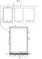
- FIG. 5 is a plan view showing a method of manufacturing the display device of Embodiment 1.
- FIG. 7 is a cross-sectional view showing the method of manufacturing the display device of Embodiment 1.
- FIG. 5 is a plan view showing a method of manufacturing the display device of Embodiment 1.
- FIG. 5 is sectional drawing which shows another manufacturing method of a display device. It is a top view which shows another manufacturing method of a display device.
- 5 is a cross-sectional view showing another configuration of the display device of Embodiment 1.
- FIG. 7 is a plan view showing a method of manufacturing a display device of Embodiment 2. It is sectional drawing in the bending part of FIG. It is sectional drawing which shows the bending state of the display device of Embodiment 2. FIG. It is sectional drawing in the parting part of FIG.
- the same layer means that it is formed in the same process (film forming step), and "the lower layer” is formed in the process before the layer to be compared “Upper layer” means being formed in a process later than the layer to be compared.
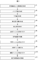
- FIG. 1 is a flowchart showing an example of a method of manufacturing a display device.
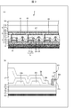
- FIG. 2 is a cross-sectional view showing a configuration example of a display unit of the display device.
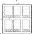
- FIG. 3 is a plan view showing a method of manufacturing a display device.
- the resin layer 12 is formed on the light transmitting support substrate 13 (for example, mother glass) (step S1).
- the barrier layer 3 is formed (step S2).
- the TFT layer 4 is formed (step S3).
- a top emission type light emitting element layer for example, an OLED element layer
- the sealing layer 6 is formed (step S5).
- an upper film is attached on the sealing layer 6 (step S6).
- the lower surface of the resin layer 12 is irradiated with laser light through the support substrate to reduce the bonding force between the support substrate 13 and the resin layer 12, and the support substrate 13 is peeled off from the resin layer 12 (step S7).
- the lower film 10 is attached to the lower surface of the resin layer 12 (step S8).
- the laminate 7 including the lower surface film 10, the resin layer 12, the barrier layer 3, the TFT layer 4, the light emitting element layer 5, and the sealing layer 6 is divided by a dividing line BL (see FIG. 3) Obtained (step S9).
- the functional film 39 is attached to the obtained piece (step S10).
- an electronic circuit board for example, an IC chip
- the terminal for external connection step S11
- the below-mentioned display device manufacturing apparatus performs said each step.
- a polyimide etc. are mentioned, for example.
- a polyethylene terephthalate (PET) is mentioned, for example.
- the barrier layer 3 is a layer that prevents foreign matter such as water and oxygen from reaching the TFT layer 4 and the light emitting element layer 5, and for example, a silicon oxide film, a silicon nitride film, or a silicon oxynitride film formed by CVD. It can be composed of a film or a laminated film of these.
- the TFT layer 4 includes the semiconductor film 15, the inorganic insulating film 16 (gate insulating film) above the semiconductor film 15, the gate electrode GE above the inorganic insulating film 16, and the inorganic insulating layer above the gate electrode GE.
- the planarizing film 21 (interlayer insulating film).
- a terminal used for connection to an electronic circuit board such as an IC chip, an FPC, etc., and a terminal wiring for connecting the terminal and the wiring of the display area DA are formed.
- the semiconductor film 15 is made of, for example, low temperature polysilicon (LTPS) or an oxide semiconductor.
- FIG. 2 shows a TFT having a semiconductor film 15 as a channel in a top gate structure, it may have a bottom gate structure (for example, when the channel of the TFT is an oxide semiconductor).
- the thin film transistor Tr (TFT) is configured to include the semiconductor film 15, the inorganic insulating film 16, and the gate electrode GE.
- Al aluminum (Al), tungsten (W), molybdenum (Mo), tantalum (Ta), chromium (Cr), titanium (Ti), the gate electrode GE, the capacitance electrode CE, the source wiring SH, the terminal and the terminal wiring It is comprised by the single layer film or laminated film of the metal containing at least one of copper (Cu).
- the inorganic insulating films 16, 18 and 20 can be formed of, for example, a silicon oxide (SiOx) film, a silicon nitride (SiNx) film, or a laminated film thereof formed by a CVD method.
- SiOx silicon oxide
- SiNx silicon nitride
- the planarizing film 21 can be made of, for example, a coatable photosensitive organic material such as polyimide or acrylic.
- the light emitting element layer 5 (for example, an organic light emitting diode layer) includes an anode 22 above the planarization film 21, an insulating anode cover film 23 covering the edge of the anode 22, and an EL (electro A light emitting element (e.g., OLED: organic light emitting diode) including a luminescent layer 24 and a cathode 25 above the EL layer 24 and including an island-like anode 22, an EL layer 24 and a cathode 25 for each sub-pixel And a sub-pixel circuit for driving the same.
- the anode cover film 23 can be made of, for example, a coatable photosensitive organic material such as polyimide or acrylic.
- the EL layer 24 is configured, for example, by laminating a hole injection layer, a hole transport layer, a light emitting layer, an electron transport layer, and an electron injection layer in order from the lower layer side.
- the light emitting layer is formed in an island shape for each sub-pixel by a vapor deposition method or an inkjet method.
- the other layers are formed in island or solid (common layer).
- the structure which does not form one or more layers among a positive hole injection layer, a positive hole transport layer, an electron carrying layer, and an electron injection layer is also possible.
- the anode (anode) 22 is formed, for example, by laminating ITO (Indium Tin Oxide) and Ag (silver) or an alloy containing Ag, and has light reflectivity (described in detail later).
- the cathode 25 can be made of a translucent conductive material such as MgAg alloy (very thin film), ITO (Indium Tin Oxide), IZO (Indium zinc Oxide), or the like.
- the drive current between the anode 22 and the cathode 25 causes holes and electrons to recombine in the EL layer 24 and the resulting excitons fall to the ground state, whereby light is generated. Released. Since the cathode 25 is translucent and the anode 22 is light reflective, the light emitted from the EL layer 24 is directed upward to be top emission.
- the light emitting element layer 5 is not limited to forming an OLED element, and may form an inorganic light emitting diode or a quantum dot light emitting diode.
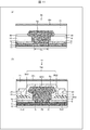
- the sealing layer 6 is translucent, and the inorganic sealing film 26 covering the cathode 25, the organic sealing film 27 above the inorganic sealing film 26, and the inorganic sealing above the organic sealing film 27. And a membrane 28.
- the sealing layer 6 covering the light emitting element layer 5 prevents the penetration of foreign matter such as water and oxygen into the light emitting element layer 5.
- the inorganic sealing film 26 and the inorganic sealing film 28 can each be formed of, for example, a silicon oxide film, a silicon nitride film, a silicon oxynitride film, or a laminated film thereof formed by CVD.
- the organic sealing film 27 is a translucent organic film having a planarization effect, and can be made of a coatable organic material such as acrylic.
- the lower surface film 10 is for adhering to the lower surface of the resin layer 12 after peeling off the support substrate to realize a display device excellent in flexibility.
- Examples of the material include PET and the like.
- the functional film 39 has, for example, an optical compensation function, a touch sensor function, a protection function, and the like.
- step S5 the case of manufacturing a flexible display device
- step S9 the process proceeds from step S5 to step S9 in FIG.
- FIG. 4 is a cross-sectional view showing the method for manufacturing the display device of Embodiment 1.
- FIG. 5 is a plan view showing the method for manufacturing the display device of Embodiment 1.
- FIG. As shown in FIGS. 3 and 4, in step S4 in FIG. 1, double banks 23b and 23c (convex structures surrounding the display area DA) are formed in the frame area (non-display area) NA.
- the banks 23b and 23c are formed (in the same step) in the same layer as the anode edge cover 23 using, for example, polyimide.
- the banks 23b and 23c function as a liquid stopper when the organic sealing film 27 is applied by inkjet.
- the frame-shaped organic edge film 21f is formed in the frame area NA in the area outside the banks 23b and 23c in plan view.
- the organic edge film 21 f is formed in the same layer (in the same step) as the planarizing film 21 of FIG. 2 using, for example, acrylic.
- step S5 of FIG. 1 the inorganic sealing film 26 (first inorganic sealing film), the organic sealing film 27, and the inorganic sealing film 28 (second inorganic) are formed above the light emitting element layer formed in step S4.
- a sealing film is formed in this order.
- the inorganic sealing film 28 is formed to cover the whole of the organic sealing film 27, the end of the inorganic sealing film 26, and the organic edge film 21f.
- the portion 28k not overlapping with the organic edge film 21f is a silicon nitride film
- the portion 28f overlapping with the organic edge film 21f is a silicon inorganic film containing oxygen.
- the portion 28k not overlapping with the organic edge film 21f is formed as a silicon nitride film.
- the covering portion 28f absorbs moisture from the organic edge film 21f (for example, an acrylic film), and is formed as a silicon oxide film or silicon oxynitride (SiON).
- the terminal portion 44 including a plurality of terminals to which an external signal is input is provided on one side of the frame area NA, but the inorganic sealing film 28 is formed of the display area DA using the mask MS. It is formed so as to cover all and all parts of the frame area NA other than the terminal part 44.
- the mask MS has an opening Mk common to a plurality of panel areas, and the inorganic sealing film 28 is formed in the area of the opening Mk.
- the mask MS has the shielding portion SK at a position corresponding to the terminal portion 44, and the inorganic sealing film 28 is not formed on the terminal portion 44.
- the silicon nitride film is high in compactness and excellent in sealing performance, but is hard and easily cracked at the time of division.
- the silicon oxide film is inferior in sealing performance to the silicon nitride film, it is softer than the silicon nitride film, and a crack does not easily occur at the time of division. Therefore, in step S9, as shown in FIGS.
- the end 28f of the inorganic sealing film 28 (the portion of the silicon oxide film overlapping the organic edge film 21f) and the organic edge film 21f (acrylic film)
- the overlapping dividing lines BL By dividing the laminated body 7 in the thickness direction (for example, laser division) by the overlapping dividing lines BL, it becomes difficult for a crack to be generated in the sealing layer 6 (in particular, the inorganic sealing film 28).
- the end surface 28e of the inorganic sealing film 28 covering the upper surface of the organic edge film 21f and the end surface 21e of the organic edge film are aligned. become.
- the fact that two or more end faces are aligned means that they are in the same plane (partial cross section).
- the end face 28e of the inorganic sealing film 28 and the end face 21e of the organic edge film are continuously flush with each other, and these both end faces (21e, 28e) are the edge EX of the display device 2. It constitutes a part.
- the end face 28 e of the inorganic sealing film 28 and the end face 21 e of the organic edge film are aligned with the end face of the resin layer 12 and the end face of the TFT layer 4.
- the organic edge film 21f may have a forward tapered shape which is tapered upward, but it is desirable that the forward angle is steep (close to 90 degrees) if the shape is a forward taper. In this way, even if a crack is generated at the end (portion of the silicon oxide film) 28 f of the inorganic sealing film 28 at the time of division, this propagates to the inner portion (portion of the silicon nitride film) 28 k of the inorganic sealing film 28 It becomes difficult.
- FIG. 6 is a cross-sectional view showing another configuration of the display device of the first embodiment.
- a portion 28f (silicon oxide film) of the inorganic sealing film 28 is island-shaped on the organic edge film 21f.
- a crack occurs in a portion 28 f (silicon oxide film) of the inorganic sealing film 28 at the time of division, it is difficult for the crack to propagate to the inner portion 28 k of the inorganic sealing film 28.
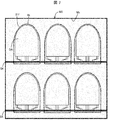
- FIG. 7 is a plan view showing another method of manufacturing a display device. Even in the case of forming a deformed panel (display device) in which a part of the edge is curved as shown in FIG. 7, a mask MS having a common opening Mk in a plurality of panel regions similar to FIG. 5 can be used. It is conceivable to prepare a mask having a curved shielding portion in order to prevent a crack at the time of division (do not form a sealing film of silicon nitride at the division location) for an odd-shaped panel. When the organic edge film 21f is formed in a curved shape along the curved edge, the portion 28f of the inorganic sealing film formed on the organic edge film 21f becomes a flexible silicon oxide film. Less likely to crack.
- FIG. 8 is a cross-sectional view showing a modification of the display device of the first embodiment.
- the inorganic sealing film 26 is formed inside the edge of the inorganic sealing film 28 in FIGS. 2 and 3, the present invention is not limited to this. As shown in FIG. 8, the inorganic sealing film 26 and the inorganic sealing film 28 may have the same pattern.
- the end surface 28e of the inorganic sealing film 28, the end surface 26e of the inorganic sealing film 26 covering the top surface of the organic edge film 21f, and the end surface 21e of the organic edge film are continuously flush.
- These end faces (28e, 26e, 21f) constitute a part of the edge EX of the display device 2.
- the end portion 26 f (portion overlapping the organic edge film 21 f) of the inorganic sealing film 26 is a flexible silicon oxide film, it is difficult for a crack to occur in the sealing layer 6 at the time of division.
- a mask having the same shape can be used to form the inorganic sealing film 26 and the inorganic sealing film 28.
- FIG. 9 is a block diagram showing the configuration of a display device manufacturing apparatus.
- the display device manufacturing apparatus 70 includes a film forming apparatus 76, a dividing apparatus 80, and a controller 72 that controls these apparatuses, and the film forming apparatus 76 performs steps S1 to S1 in FIG. S6 is performed, and the dividing device 80 performs step S9.
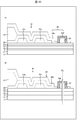
- Second Embodiment 10 is a plan view showing a method of manufacturing the display device of Embodiment 2
- FIG. 11 is a cross-sectional view of a bent portion in FIG. 10
- FIG. 9 is a cross section showing a bent state of the display device of Embodiment 2.
- the support substrate 13 As shown in FIGS. 10 and 11, in the frame area (frame area) NA of the laminated body 7, the support substrate 13, the resin layer 12, the barrier layer 3, the inorganic insulating film 16/18/20, the organic reinforcing film Qc, A terminal TM, a terminal wiring TW connected to the terminal TM, a planarizing film 21 and a portion 28c of the inorganic sealing film 28 are provided, and a bent portion CL is provided in the frame area NA.
- the terminal TM is connected to the display area DA by a terminal wire TW which passes through the bent portion CL.
- the organic reinforcing film Qc is made of, for example, an organic material such as polyimide or acrylic, and is formed above the inorganic insulating film 20 and below the terminals TM and TM.
- each of the barrier layer 3 and the inorganic insulating films 16, 18, and 20 is penetrated to enhance the flexibility, and the penetrating portion of the barrier layer 3 and the inorganic insulating film 16
- An organic reinforcing film Qc is formed to fill the penetrating portion, the penetrating portion of the inorganic insulating film 18, and the penetrating portion of the inorganic insulating film 20.
- the terminal wiring TW includes a wiring WS1 and a wiring WS2 located on both sides of the bent portion CL, and a wiring WS3 electrically connected to each of the first wiring WS1 and the second wiring WS2 through the bent portion CL.
- the wiring WS1 and the wiring WS2 are formed in the same layer as the gate electrode GE (see FIG. 2) included in the TFT layer 4.
- the wiring WS3 is formed in the same layer as the source wiring SH (see FIG. 2) included in the TFT layer 4 and the terminal TM.
- the wiring WS3 passes from one side of the bent portion CL to the other side of the bent portion CL through the organic reinforcing film Qc, and in the bent portion CL, the organic reinforcing film Qc and the flattening film 21 (for example, And the acrylic film).
- One end of the wiring WS3 is connected to the wiring WS1 by the contact hole Hc1 penetrating the inorganic insulating films 18 and 20, and the other end of the wiring WS3 is connected to the wiring WS2 by the contact hole Hc2 penetrating the inorganic insulating films 18 and 20.
- Ru In the bent portion CL, a portion 28 c of the inorganic sealing film 28 is formed on the planarization film 21.
- the display device 2 is bent 180 degrees by the bending portion CL after step S11, whereby the terminal portion 44 on which the electronic circuit board 50 (IC chip or flexible printed circuit board) is mounted turns around the back surface. , Narrowing of the frame is realized.
- FIG. 13 is a cross-sectional view showing the divided portion in FIG.
- the organic edge film Qf is formed in the area outside the banks 23b and 23c in plan view.
- the organic edge film Qf is formed (in the same step) in the same layer as the organic reinforcing film Qc of FIG. 11 using, for example, acrylic.
- the inorganic sealing film 26, the organic sealing film 27, and the inorganic sealing film 28 are formed in this order on the upper layer than the light emitting element layer formed in step S4.
- the inorganic sealing film 28 is formed to cover the whole of the organic sealing film 27, the end of the inorganic sealing film 26, and the organic edge film Qf.
- the portion 28k not overlapping with the organic edge film Qf is a silicon nitride film
- the portion 28f overlapping with the organic edge film Qf is a silicon inorganic film containing oxygen
- the flattening film 21 is formed at the bent portion CL.
- the overlapping portion 28c is a silicon inorganic film containing oxygen.
- the portion 28k not overlapping with the organic edge film Qf is formed as a silicon nitride film.
- the covering portion 28f absorbs moisture from the organic edge film Qf (for example, an acrylic film) and is formed as a silicon oxide film or silicon oxynitride (SiON).
- the portion 28c covering the planarization film 21 of FIG. 12 also absorbs moisture from the planarization film 21 (for example, an acrylic film), and is formed as a silicon oxide film or silicon oxynitride (SiON).
- the end 28f portion of the silicon oxide film
- a crack is less likely to be generated in the sealing layer 6 (in particular, the inorganic sealing film 28).
- the flexibility of the bent portion CL can be maintained while protecting the wiring WS3 by the portion 28c (portion of the silicon oxide film) of the inorganic sealing film 28.
- the electro-optical elements included in the display device according to the present embodiment are not particularly limited.
- the display device according to the present embodiment includes, for example, an organic EL (Electro Luminescence) display provided with an OLED (Organic Light Emitting Diode) as an electro-optical element, and an inorganic light emitting diode as an electro-optical element Inorganic EL display, a QLED display provided with a QLED (Quantum dot Light Emitting Diode) as an electro-optical element, and the like.
- a terminal portion including a plurality of terminals to which an external signal is input is provided on one side of the frame region,
- the first inorganic sealing film overlaps the top surface of the organic edge film, and the end surface of the organic edge film and the end surface of the first inorganic sealing film are aligned.
- the display device according to aspect 1 or 2 for example, in which the formation patterns of the first inorganic sealing film and the second inorganic sealing film are the same.
- Aspect 7 The display device according to, for example, the sixth aspect, wherein the first inorganic sealing film is a silicon inorganic film in which a portion overlapping the organic edge film is a silicon inorganic film containing oxygen, and a portion not overlapping the organic edge film is a silicon nitride film.
- the first inorganic sealing film is a silicon inorganic film in which a portion overlapping the organic edge film is a silicon inorganic film containing oxygen, and a portion not overlapping the organic edge film is a silicon nitride film.
- a bent portion is provided on the display area side of the terminal portion,
- the display device according to, for example, the second aspect, wherein the terminal wiring passing through the bent portion is sandwiched between an organic reinforcing film and a planarization film, and the second inorganic sealing film is formed on the planarization film.
- the display device for example, in which the second inorganic sealing film is a silicon inorganic film in which a portion overlapping the planarization film is a silicon inorganic film.
- a laminate comprising a TFT layer, a light emitting layer above the TFT layer, a first inorganic sealing film above the light emitting layer, and a second inorganic sealing film above the first inorganic sealing film
- a method of manufacturing a display device including the step of dividing Forming an organic edge film on the periphery of the frame area surrounding the display area; Forming the second inorganic sealing film so as to overlap the organic edge film; Cutting the laminate so as to pass through the second inorganic sealing film and the organic edge film.
- the laminate includes a plurality of panel areas, A method of manufacturing a display device according to, for example, an eleventh aspect, wherein the second inorganic sealing film is formed using a mask having a common opening in the plurality of panel regions.
Landscapes
- Engineering & Computer Science (AREA)
- Physics & Mathematics (AREA)
- Manufacturing & Machinery (AREA)
- Microelectronics & Electronic Packaging (AREA)
- General Physics & Mathematics (AREA)
- Theoretical Computer Science (AREA)
- Optics & Photonics (AREA)
- Electroluminescent Light Sources (AREA)
Abstract
Ce dispositif d'affichage est pourvu : d'une couche TFT (4) ; d'une couche électroluminescente située au-dessus de la couche TFT ; d'un premier film d'étanchéité inorganique (26) situé au-dessus de la couche électroluminescente ; et d'un second film d'étanchéité inorganique (28) situé au-dessus du premier film d'étanchéité inorganique, un film de bord organique (21f) étant disposé sur le bord périphérique d'une zone de cadre qui entoure une zone d'affichage, le second film d'étanchéité inorganique chevauchant la surface supérieure du film de bord organique, et une surface d'extrémité (Ta) du film de bord organique ainsi qu'une surface d'extrémité (Tb) du second film d'étanchéité organique étant alignées l'une avec l'autre.
Priority Applications (2)
| Application Number | Priority Date | Filing Date | Title |
|---|---|---|---|
| PCT/JP2017/035729 WO2019064591A1 (fr) | 2017-09-29 | 2017-09-29 | Dispositif d'affichage et procédé de fabrication de dispositif d'affichage |
| US16/473,262 US20200152910A1 (en) | 2017-09-29 | 2017-09-29 | Display device |
Applications Claiming Priority (1)
| Application Number | Priority Date | Filing Date | Title |
|---|---|---|---|
| PCT/JP2017/035729 WO2019064591A1 (fr) | 2017-09-29 | 2017-09-29 | Dispositif d'affichage et procédé de fabrication de dispositif d'affichage |
Publications (1)
| Publication Number | Publication Date |
|---|---|
| WO2019064591A1 true WO2019064591A1 (fr) | 2019-04-04 |
Family
ID=65903592
Family Applications (1)
| Application Number | Title | Priority Date | Filing Date |
|---|---|---|---|
| PCT/JP2017/035729 WO2019064591A1 (fr) | 2017-09-29 | 2017-09-29 | Dispositif d'affichage et procédé de fabrication de dispositif d'affichage |
Country Status (2)
| Country | Link |
|---|---|
| US (1) | US20200152910A1 (fr) |
| WO (1) | WO2019064591A1 (fr) |
Cited By (1)
| Publication number | Priority date | Publication date | Assignee | Title |
|---|---|---|---|---|
| TWI715149B (zh) * | 2019-08-14 | 2021-01-01 | 友達光電股份有限公司 | 顯示裝置 |
Families Citing this family (3)
| Publication number | Priority date | Publication date | Assignee | Title |
|---|---|---|---|---|
| US20190267570A1 (en) * | 2018-02-27 | 2019-08-29 | Wuhan China Star Optoelectronics Semiconductor Display Technology Co., Ltd. | Oled display device |
| WO2019171581A1 (fr) * | 2018-03-09 | 2019-09-12 | シャープ株式会社 | Dispositif d'affichage |
| US11997889B2 (en) * | 2018-03-30 | 2024-05-28 | Sharp Kabushiki Kaisha | Display device |
Citations (5)
| Publication number | Priority date | Publication date | Assignee | Title |
|---|---|---|---|---|
| JP2010003682A (ja) * | 2008-05-21 | 2010-01-07 | Canon Inc | 有機発光装置の製造方法 |
| JP2011008969A (ja) * | 2009-06-23 | 2011-01-13 | Canon Inc | 表示装置 |
| JP2012128006A (ja) * | 2010-12-13 | 2012-07-05 | Sony Corp | 表示装置及び電子機器 |
| JP2014170686A (ja) * | 2013-03-04 | 2014-09-18 | Toshiba Corp | 表示素子の製造方法、表示素子及び表示装置 |
| US20150034935A1 (en) * | 2013-07-31 | 2015-02-05 | Samsung Display Co., Ltd. | Flexible display device and manufacturing method thereof |
Family Cites Families (6)
| Publication number | Priority date | Publication date | Assignee | Title |
|---|---|---|---|---|
| KR102572722B1 (ko) * | 2016-05-11 | 2023-09-01 | 삼성디스플레이 주식회사 | 디스플레이 장치 |
| CN106784377B (zh) * | 2016-12-28 | 2018-06-29 | 上海天马有机发光显示技术有限公司 | 一种柔性显示面板、显示装置和柔性显示面板的制作方法 |
| KR102416550B1 (ko) * | 2017-04-28 | 2022-07-05 | 삼성디스플레이 주식회사 | 편광층, 이를 구비하는 표시 장치 및 표시 장치의 제조 방법 |
| JP2019012098A (ja) * | 2017-06-29 | 2019-01-24 | 株式会社ジャパンディスプレイ | 表示装置 |
| JP6805099B2 (ja) * | 2017-09-08 | 2020-12-23 | 株式会社Joled | 有機el表示パネル、有機el表示装置、およびその製造方法 |
| KR102417112B1 (ko) * | 2017-09-28 | 2022-07-06 | 삼성디스플레이 주식회사 | 디스플레이 장치 |
-
2017
- 2017-09-29 US US16/473,262 patent/US20200152910A1/en not_active Abandoned
- 2017-09-29 WO PCT/JP2017/035729 patent/WO2019064591A1/fr active Application Filing
Patent Citations (5)
| Publication number | Priority date | Publication date | Assignee | Title |
|---|---|---|---|---|
| JP2010003682A (ja) * | 2008-05-21 | 2010-01-07 | Canon Inc | 有機発光装置の製造方法 |
| JP2011008969A (ja) * | 2009-06-23 | 2011-01-13 | Canon Inc | 表示装置 |
| JP2012128006A (ja) * | 2010-12-13 | 2012-07-05 | Sony Corp | 表示装置及び電子機器 |
| JP2014170686A (ja) * | 2013-03-04 | 2014-09-18 | Toshiba Corp | 表示素子の製造方法、表示素子及び表示装置 |
| US20150034935A1 (en) * | 2013-07-31 | 2015-02-05 | Samsung Display Co., Ltd. | Flexible display device and manufacturing method thereof |
Cited By (1)
| Publication number | Priority date | Publication date | Assignee | Title |
|---|---|---|---|---|
| TWI715149B (zh) * | 2019-08-14 | 2021-01-01 | 友達光電股份有限公司 | 顯示裝置 |
Also Published As
| Publication number | Publication date |
|---|---|
| US20200152910A1 (en) | 2020-05-14 |
Similar Documents
| Publication | Publication Date | Title |
|---|---|---|
| JP7038125B2 (ja) | 表示デバイス、表示デバイスの製造方法 | |
| WO2019064534A1 (fr) | Dispositif d'affichage flexible et procédé de production d'un dispositif d'affichage flexible | |
| WO2020066011A1 (fr) | Dispositif d'affichage | |
| CN111937058B (zh) | 显示设备 | |
| CN111108541B (zh) | 可弯曲性显示装置以及可弯曲性显示装置的制造方法 | |
| JPWO2018179168A1 (ja) | 表示デバイス、表示デバイスの製造方法、表示デバイスの製造装置、成膜装置 | |
| WO2019064591A1 (fr) | Dispositif d'affichage et procédé de fabrication de dispositif d'affichage | |
| WO2019064342A1 (fr) | Dispositif d'affichage, procédé de fabrication d'un dispositif d'affichage et appareil de fabrication d'un dispositif d'affichage | |
| WO2019187159A1 (fr) | Dispositif d'affichage | |
| WO2019150503A1 (fr) | Dispositif d'affichage | |
| WO2019021467A1 (fr) | Dispositif d'affichage, procédé de fabrication d'un dispositif d'affichage, et appareil de fabrication d'un dispositif d'affichage | |
| US11538894B2 (en) | Display device with overlapped wiring lines at periphery of cutout region | |
| WO2018179132A1 (fr) | Procédé de production de dispositif d'affichage, dispositif d'affichage, appareil de production de dispositif d'affichage et appareil de déposition | |
| CN112425264B (zh) | 显示装置 | |
| WO2019187156A1 (fr) | Dispositif d'affichage | |
| US10621893B2 (en) | Display device, manufacturing method for display device, manufacturing apparatus of display device, mounting device, and controller | |
| WO2019038884A1 (fr) | Dispositif d'affichage | |
| US10847733B2 (en) | Display device | |
| WO2018179175A1 (fr) | Dispositif d'affichage, procédé de fabrication de dispositif d'affichage, appareil de fabrication de dispositif d'affichage, appareil de dépôt et dispositif de commande | |
| WO2019130427A1 (fr) | Dispositif d'affichage | |
| US10777633B2 (en) | Display device, display device manufacturing method, and display device manufacturing apparatus | |
| US12022680B2 (en) | Display device | |
| KR102707494B1 (ko) | 표시 장치 | |
| WO2020202281A1 (fr) | Dispositif d'affichage | |
| WO2019187161A1 (fr) | Dispositif d'affichage |
Legal Events
| Date | Code | Title | Description |
|---|---|---|---|
| 121 | Ep: the epo has been informed by wipo that ep was designated in this application |
Ref document number: 17926509 Country of ref document: EP Kind code of ref document: A1 |
|
| NENP | Non-entry into the national phase |
Ref country code: DE |
|
| 122 | Ep: pct application non-entry in european phase |
Ref document number: 17926509 Country of ref document: EP Kind code of ref document: A1 |
|
| NENP | Non-entry into the national phase |
Ref country code: JP |