WO2019037546A1 - Vapor deposition device and vapor deposition method - Google Patents
Vapor deposition device and vapor deposition method Download PDFInfo
- Publication number
- WO2019037546A1 WO2019037546A1 PCT/CN2018/094458 CN2018094458W WO2019037546A1 WO 2019037546 A1 WO2019037546 A1 WO 2019037546A1 CN 2018094458 W CN2018094458 W CN 2018094458W WO 2019037546 A1 WO2019037546 A1 WO 2019037546A1
- Authority
- WO
- WIPO (PCT)
- Prior art keywords
- vapor deposition
- substrate
- sub
- evaporation
- material particles
- Prior art date
Links
Images


Classifications
-
- C—CHEMISTRY; METALLURGY
- C23—COATING METALLIC MATERIAL; COATING MATERIAL WITH METALLIC MATERIAL; CHEMICAL SURFACE TREATMENT; DIFFUSION TREATMENT OF METALLIC MATERIAL; COATING BY VACUUM EVAPORATION, BY SPUTTERING, BY ION IMPLANTATION OR BY CHEMICAL VAPOUR DEPOSITION, IN GENERAL; INHIBITING CORROSION OF METALLIC MATERIAL OR INCRUSTATION IN GENERAL
- C23C—COATING METALLIC MATERIAL; COATING MATERIAL WITH METALLIC MATERIAL; SURFACE TREATMENT OF METALLIC MATERIAL BY DIFFUSION INTO THE SURFACE, BY CHEMICAL CONVERSION OR SUBSTITUTION; COATING BY VACUUM EVAPORATION, BY SPUTTERING, BY ION IMPLANTATION OR BY CHEMICAL VAPOUR DEPOSITION, IN GENERAL
- C23C14/00—Coating by vacuum evaporation, by sputtering or by ion implantation of the coating forming material
- C23C14/04—Coating on selected surface areas, e.g. using masks
- C23C14/042—Coating on selected surface areas, e.g. using masks using masks
-
- C—CHEMISTRY; METALLURGY
- C23—COATING METALLIC MATERIAL; COATING MATERIAL WITH METALLIC MATERIAL; CHEMICAL SURFACE TREATMENT; DIFFUSION TREATMENT OF METALLIC MATERIAL; COATING BY VACUUM EVAPORATION, BY SPUTTERING, BY ION IMPLANTATION OR BY CHEMICAL VAPOUR DEPOSITION, IN GENERAL; INHIBITING CORROSION OF METALLIC MATERIAL OR INCRUSTATION IN GENERAL
- C23C—COATING METALLIC MATERIAL; COATING MATERIAL WITH METALLIC MATERIAL; SURFACE TREATMENT OF METALLIC MATERIAL BY DIFFUSION INTO THE SURFACE, BY CHEMICAL CONVERSION OR SUBSTITUTION; COATING BY VACUUM EVAPORATION, BY SPUTTERING, BY ION IMPLANTATION OR BY CHEMICAL VAPOUR DEPOSITION, IN GENERAL
- C23C14/00—Coating by vacuum evaporation, by sputtering or by ion implantation of the coating forming material
- C23C14/22—Coating by vacuum evaporation, by sputtering or by ion implantation of the coating forming material characterised by the process of coating
- C23C14/24—Vacuum evaporation
- C23C14/32—Vacuum evaporation by explosion; by evaporation and subsequent ionisation of the vapours, e.g. ion-plating
-
- C—CHEMISTRY; METALLURGY
- C23—COATING METALLIC MATERIAL; COATING MATERIAL WITH METALLIC MATERIAL; CHEMICAL SURFACE TREATMENT; DIFFUSION TREATMENT OF METALLIC MATERIAL; COATING BY VACUUM EVAPORATION, BY SPUTTERING, BY ION IMPLANTATION OR BY CHEMICAL VAPOUR DEPOSITION, IN GENERAL; INHIBITING CORROSION OF METALLIC MATERIAL OR INCRUSTATION IN GENERAL
- C23C—COATING METALLIC MATERIAL; COATING MATERIAL WITH METALLIC MATERIAL; SURFACE TREATMENT OF METALLIC MATERIAL BY DIFFUSION INTO THE SURFACE, BY CHEMICAL CONVERSION OR SUBSTITUTION; COATING BY VACUUM EVAPORATION, BY SPUTTERING, BY ION IMPLANTATION OR BY CHEMICAL VAPOUR DEPOSITION, IN GENERAL
- C23C14/00—Coating by vacuum evaporation, by sputtering or by ion implantation of the coating forming material
- C23C14/04—Coating on selected surface areas, e.g. using masks
- C23C14/048—Coating on selected surface areas, e.g. using masks using irradiation by energy or particles
-
- C—CHEMISTRY; METALLURGY
- C23—COATING METALLIC MATERIAL; COATING MATERIAL WITH METALLIC MATERIAL; CHEMICAL SURFACE TREATMENT; DIFFUSION TREATMENT OF METALLIC MATERIAL; COATING BY VACUUM EVAPORATION, BY SPUTTERING, BY ION IMPLANTATION OR BY CHEMICAL VAPOUR DEPOSITION, IN GENERAL; INHIBITING CORROSION OF METALLIC MATERIAL OR INCRUSTATION IN GENERAL
- C23C—COATING METALLIC MATERIAL; COATING MATERIAL WITH METALLIC MATERIAL; SURFACE TREATMENT OF METALLIC MATERIAL BY DIFFUSION INTO THE SURFACE, BY CHEMICAL CONVERSION OR SUBSTITUTION; COATING BY VACUUM EVAPORATION, BY SPUTTERING, BY ION IMPLANTATION OR BY CHEMICAL VAPOUR DEPOSITION, IN GENERAL
- C23C14/00—Coating by vacuum evaporation, by sputtering or by ion implantation of the coating forming material
- C23C14/06—Coating by vacuum evaporation, by sputtering or by ion implantation of the coating forming material characterised by the coating material
- C23C14/12—Organic material
-
- C—CHEMISTRY; METALLURGY
- C23—COATING METALLIC MATERIAL; COATING MATERIAL WITH METALLIC MATERIAL; CHEMICAL SURFACE TREATMENT; DIFFUSION TREATMENT OF METALLIC MATERIAL; COATING BY VACUUM EVAPORATION, BY SPUTTERING, BY ION IMPLANTATION OR BY CHEMICAL VAPOUR DEPOSITION, IN GENERAL; INHIBITING CORROSION OF METALLIC MATERIAL OR INCRUSTATION IN GENERAL
- C23C—COATING METALLIC MATERIAL; COATING MATERIAL WITH METALLIC MATERIAL; SURFACE TREATMENT OF METALLIC MATERIAL BY DIFFUSION INTO THE SURFACE, BY CHEMICAL CONVERSION OR SUBSTITUTION; COATING BY VACUUM EVAPORATION, BY SPUTTERING, BY ION IMPLANTATION OR BY CHEMICAL VAPOUR DEPOSITION, IN GENERAL
- C23C14/00—Coating by vacuum evaporation, by sputtering or by ion implantation of the coating forming material
- C23C14/22—Coating by vacuum evaporation, by sputtering or by ion implantation of the coating forming material characterised by the process of coating
- C23C14/24—Vacuum evaporation
- C23C14/243—Crucibles for source material
-
- C—CHEMISTRY; METALLURGY
- C23—COATING METALLIC MATERIAL; COATING MATERIAL WITH METALLIC MATERIAL; CHEMICAL SURFACE TREATMENT; DIFFUSION TREATMENT OF METALLIC MATERIAL; COATING BY VACUUM EVAPORATION, BY SPUTTERING, BY ION IMPLANTATION OR BY CHEMICAL VAPOUR DEPOSITION, IN GENERAL; INHIBITING CORROSION OF METALLIC MATERIAL OR INCRUSTATION IN GENERAL
- C23C—COATING METALLIC MATERIAL; COATING MATERIAL WITH METALLIC MATERIAL; SURFACE TREATMENT OF METALLIC MATERIAL BY DIFFUSION INTO THE SURFACE, BY CHEMICAL CONVERSION OR SUBSTITUTION; COATING BY VACUUM EVAPORATION, BY SPUTTERING, BY ION IMPLANTATION OR BY CHEMICAL VAPOUR DEPOSITION, IN GENERAL
- C23C14/00—Coating by vacuum evaporation, by sputtering or by ion implantation of the coating forming material
- C23C14/22—Coating by vacuum evaporation, by sputtering or by ion implantation of the coating forming material characterised by the process of coating
- C23C14/24—Vacuum evaporation
- C23C14/32—Vacuum evaporation by explosion; by evaporation and subsequent ionisation of the vapours, e.g. ion-plating
- C23C14/325—Electric arc evaporation
-
- C—CHEMISTRY; METALLURGY
- C23—COATING METALLIC MATERIAL; COATING MATERIAL WITH METALLIC MATERIAL; CHEMICAL SURFACE TREATMENT; DIFFUSION TREATMENT OF METALLIC MATERIAL; COATING BY VACUUM EVAPORATION, BY SPUTTERING, BY ION IMPLANTATION OR BY CHEMICAL VAPOUR DEPOSITION, IN GENERAL; INHIBITING CORROSION OF METALLIC MATERIAL OR INCRUSTATION IN GENERAL
- C23C—COATING METALLIC MATERIAL; COATING MATERIAL WITH METALLIC MATERIAL; SURFACE TREATMENT OF METALLIC MATERIAL BY DIFFUSION INTO THE SURFACE, BY CHEMICAL CONVERSION OR SUBSTITUTION; COATING BY VACUUM EVAPORATION, BY SPUTTERING, BY ION IMPLANTATION OR BY CHEMICAL VAPOUR DEPOSITION, IN GENERAL
- C23C14/00—Coating by vacuum evaporation, by sputtering or by ion implantation of the coating forming material
- C23C14/22—Coating by vacuum evaporation, by sputtering or by ion implantation of the coating forming material characterised by the process of coating
- C23C14/54—Controlling or regulating the coating process
- C23C14/542—Controlling the film thickness or evaporation rate
- C23C14/543—Controlling the film thickness or evaporation rate using measurement on the vapor source
-
- C—CHEMISTRY; METALLURGY
- C23—COATING METALLIC MATERIAL; COATING MATERIAL WITH METALLIC MATERIAL; CHEMICAL SURFACE TREATMENT; DIFFUSION TREATMENT OF METALLIC MATERIAL; COATING BY VACUUM EVAPORATION, BY SPUTTERING, BY ION IMPLANTATION OR BY CHEMICAL VAPOUR DEPOSITION, IN GENERAL; INHIBITING CORROSION OF METALLIC MATERIAL OR INCRUSTATION IN GENERAL
- C23C—COATING METALLIC MATERIAL; COATING MATERIAL WITH METALLIC MATERIAL; SURFACE TREATMENT OF METALLIC MATERIAL BY DIFFUSION INTO THE SURFACE, BY CHEMICAL CONVERSION OR SUBSTITUTION; COATING BY VACUUM EVAPORATION, BY SPUTTERING, BY ION IMPLANTATION OR BY CHEMICAL VAPOUR DEPOSITION, IN GENERAL
- C23C14/00—Coating by vacuum evaporation, by sputtering or by ion implantation of the coating forming material
- C23C14/22—Coating by vacuum evaporation, by sputtering or by ion implantation of the coating forming material characterised by the process of coating
- C23C14/54—Controlling or regulating the coating process
- C23C14/548—Controlling the composition
-
- C—CHEMISTRY; METALLURGY
- C23—COATING METALLIC MATERIAL; COATING MATERIAL WITH METALLIC MATERIAL; CHEMICAL SURFACE TREATMENT; DIFFUSION TREATMENT OF METALLIC MATERIAL; COATING BY VACUUM EVAPORATION, BY SPUTTERING, BY ION IMPLANTATION OR BY CHEMICAL VAPOUR DEPOSITION, IN GENERAL; INHIBITING CORROSION OF METALLIC MATERIAL OR INCRUSTATION IN GENERAL
- C23C—COATING METALLIC MATERIAL; COATING MATERIAL WITH METALLIC MATERIAL; SURFACE TREATMENT OF METALLIC MATERIAL BY DIFFUSION INTO THE SURFACE, BY CHEMICAL CONVERSION OR SUBSTITUTION; COATING BY VACUUM EVAPORATION, BY SPUTTERING, BY ION IMPLANTATION OR BY CHEMICAL VAPOUR DEPOSITION, IN GENERAL
- C23C14/00—Coating by vacuum evaporation, by sputtering or by ion implantation of the coating forming material
- C23C14/22—Coating by vacuum evaporation, by sputtering or by ion implantation of the coating forming material characterised by the process of coating
- C23C14/56—Apparatus specially adapted for continuous coating; Arrangements for maintaining the vacuum, e.g. vacuum locks
- C23C14/568—Transferring the substrates through a series of coating stations
-
- H—ELECTRICITY
- H10—SEMICONDUCTOR DEVICES; ELECTRIC SOLID-STATE DEVICES NOT OTHERWISE PROVIDED FOR
- H10K—ORGANIC ELECTRIC SOLID-STATE DEVICES
- H10K50/00—Organic light-emitting devices
- H10K50/10—OLEDs or polymer light-emitting diodes [PLED]
- H10K50/11—OLEDs or polymer light-emitting diodes [PLED] characterised by the electroluminescent [EL] layers
-
- H—ELECTRICITY
- H10—SEMICONDUCTOR DEVICES; ELECTRIC SOLID-STATE DEVICES NOT OTHERWISE PROVIDED FOR
- H10K—ORGANIC ELECTRIC SOLID-STATE DEVICES
- H10K50/00—Organic light-emitting devices
- H10K50/80—Constructional details
-
- H—ELECTRICITY
- H10—SEMICONDUCTOR DEVICES; ELECTRIC SOLID-STATE DEVICES NOT OTHERWISE PROVIDED FOR
- H10K—ORGANIC ELECTRIC SOLID-STATE DEVICES
- H10K50/00—Organic light-emitting devices
- H10K50/80—Constructional details
- H10K50/84—Passivation; Containers; Encapsulations
- H10K50/844—Encapsulations
-
- H—ELECTRICITY
- H10—SEMICONDUCTOR DEVICES; ELECTRIC SOLID-STATE DEVICES NOT OTHERWISE PROVIDED FOR
- H10K—ORGANIC ELECTRIC SOLID-STATE DEVICES
- H10K71/00—Manufacture or treatment specially adapted for the organic devices covered by this subclass
-
- H—ELECTRICITY
- H10—SEMICONDUCTOR DEVICES; ELECTRIC SOLID-STATE DEVICES NOT OTHERWISE PROVIDED FOR
- H10K—ORGANIC ELECTRIC SOLID-STATE DEVICES
- H10K71/00—Manufacture or treatment specially adapted for the organic devices covered by this subclass
- H10K71/10—Deposition of organic active material
- H10K71/16—Deposition of organic active material using physical vapour deposition [PVD], e.g. vacuum deposition or sputtering
- H10K71/164—Deposition of organic active material using physical vapour deposition [PVD], e.g. vacuum deposition or sputtering using vacuum deposition
Definitions
- the present disclosure relates to the field of film preparation technology, and in particular to an evaporation device and an evaporation method.
- OLEDs organic light emitting diodes
- a large-sized OLED display is required to have a plurality of different organic luminescent materials, so a corresponding number of evaporation sources are required.
- the OLED organic evaporation chamber in the related art is a large chamber through which the space is continuous, and such a large chamber has
- One drawback is that during the long-term evaporation process, the molecules evaporating from each evaporation source will have a certain probability of diffusing in the space, leading to crosstalk between molecules, resulting in impure and ineffective failure of the materials evaporated onto the substrate. Point, it will also affect the life of the OLED and the deviation of the display color coordinates.
- An embodiment of the present disclosure provides an evaporation apparatus for depositing a pattern of a plurality of film layers on a substrate to be evaporated, the evaporation apparatus comprising:
- a particulate charging module disposed at least in the sub-vapor deposition chamber
- the microparticle charging module is configured to control the first polar charge of the vapor deposition material particles generated by the evaporation source in each sub-vapor deposition chamber.
- vapor deposition device as described above, wherein the vapor deposition device further comprises:
- An electric field forming module is configured to form a guiding electric field for driving the vapor-deposited material particles to be evaporated on the substrate.
- the electric field forming module comprises:
- a substrate charging module configured to control a charge of the second polarity of the substrate to be evaporated, and the guiding electric field is formed between the conductive separator and the substrate.
- the vapor deposition device as described above, wherein the vapor deposition device further comprises a transfer device disposed in the vapor deposition chamber; wherein the conductive spacer divides the vapor deposition chamber into a plurality of directions in a first direction a vapor deposition chamber; the transfer device transports the substrate to be evaporated in the first direction.
- the vapor deposition device as described above, wherein the transfer device includes a track extending in the first direction; the substrate to be vapor-deposited is slidably mounted on the track.
- the plurality of evaporation sources are equally spaced.
- each evaporation source is used to generate luminescent material particles capable of emitting light of a specific color.
- the embodiment of the present disclosure further provides a method for performing vapor deposition by using the vapor deposition device as described above, for depositing a pattern of a plurality of film layers on a substrate to be evaporated, the evaporation method comprising:
- a guiding electric field is formed to drive the charged vapor deposition material particles onto the substrate.
- step of forming a guiding electric field comprises:
- the substrate to be vapor-deposited is transported in a first direction, and charged vapor-deposited material particles outputted from an evaporation source of each sub-vapor deposition chamber are vapor-deposited on the substrate.
- the substrate is an organic electroluminescence display substrate
- the controlling the evaporation source located in one of the plurality of sub-vapor deposition chambers to generate the vapor deposition material particles includes: controlling an evaporation source located in one of the plurality of sub-vapor deposition chambers to generate luminescent material particles capable of emitting a specific color light;
- the pattern of forming a film layer on the substrate by vaporizing the repulsive force between the same charges of the conductive separator comprises: controlling the luminescent material particle band generated by the evaporation source located in one of the plurality of sub-vapor deposition chambers a first polarity charge, the charged luminescent material particles are vaporized on the corresponding sub-pixel of the substrate under the repulsive force between the same charges of the conductive separator of one of the plurality of sub-vapor deposition chambers A luminescent layer is formed in the area.
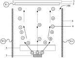
- FIG. 1 is a schematic structural view of an evaporation device according to an embodiment of the present disclosure
- FIG. 2 is a schematic structural view showing a sub-vapor deposition chamber of the vapor deposition device in the embodiment of the present disclosure
- FIG. 3 is a schematic flow chart showing an evaporation method in an embodiment of the present disclosure
- Fig. 4 is a view showing the structure of a sub-vapor deposition chamber of the vapor deposition device in the embodiment of the present disclosure.
- an evaporation apparatus for vapor-depositing a pattern of a plurality of film layers on a substrate 2 to be vapor-deposited.
- the evaporation device includes:
- each of the evaporation sources 3 is used to generate the vapor deposition material particles 4 , and the vapor deposition material particles 4 generated by the different evaporation sources 3 are different;
- a conductive separator 6 disposed between two adjacent evaporation sources 3, the conductive separator 6 is used to divide the vapor deposition chamber 1 into a plurality of sub-vapor deposition chambers 100, and the evaporation sources 3 are disposed one by one in the one-to-one correspondence Sub-vapor deposition chamber 100;
- a charge providing module for controlling the electric charge of the conductive separator 6 with a first polarity
- the microparticle charging module 5 is disposed in each sub-vapor deposition chamber 100, and the microparticle charging module 5 is configured to control the vapor-deposited material particles 4 generated by the evaporation source 3 to have a charge of a first polarity, and the charged vapor-deposited material particles 4 are electrically conductive. Under the action of the repulsive force between the charges of the separator 6, the substrate 2 is vapor-deposited to form a pattern of a film layer.
- the vapor deposition device divides the vapor deposition chamber into a plurality of sub-vapor deposition chambers through a conductive separator, and respectively sets an evaporation source in each sub-vapor deposition chamber, and controls the conductive separator and the vapor deposition material microparticles to be the same species.
- the charge is such that the vapor deposition material particles are repelled by the same kind of charge of the conductive separator, the evaporation angle of the vapor deposition material particles is reduced, the cross-flow of the vapor deposition material particles evaporated by different evaporation sources is avoided, and the vapor deposition is improved. quality.
- more vapor deposition material particles can be vapor deposited on the substrate to improve material utilization.
- the vapor deposition device of the present disclosure can avoid the crosstalk of the vapor deposition material particles evaporated by different evaporation sources, can shorten the distance between different evaporation sources, reduce the volume of the device, shorten the time consumption of the evaporation process, and improve the production efficiency. ,cut costs.
- the conductive separator utilizes the repulsive force between the same kind of electric charge to reduce the vapor deposition angle of the vapor deposition material particles, and does not affect the material properties on the substrate, especially the performance of the semiconductor material, and ensures the performance of the substrate.
- the particulate charging module 5 may specifically be an ion source, and the ion source may be selected from different types, such as a high frequency ion source and an arc discharge ion source.
- the particulate charging module 5 can also charge the non-molecular-state vapor-deposited material particles 4 in other ways.
- the vapor deposition device of the present disclosure is suitable for vapor-depositing corresponding organic light-emitting material particles in sub-pixel regions of different colors of an OLED display substrate to form a light-emitting layer capable of emitting light of a corresponding color.
- each evaporation source is used to generate luminescent material particles capable of emitting light of a particular color.
- the vapor deposition device of the present disclosure when the vapor deposition device of the present disclosure is applied to the fabrication of an OLED display substrate, the vapor deposition device may further include an evaporation source of particles for generating other organic materials such as a flat layer.
- the vapor deposition device of the present disclosure is also applicable to the fabrication of other substrates to realize vapor deposition of different vapor deposition materials on the substrate to form different film layers of the substrate 2, which are not enumerated here.
- the vapor deposition device may further include an electric field forming module for forming a guiding electric field, and the guiding electric field is used for driving the charged vapor deposition material particles 4 to be evaporated on the substrate 2 to make more steaming.
- the plating material particles 4 are deposited on the substrate 2 to further improve material utilization. At the same time, crosstalk of the vapor-deposited material particles 4 which are evaporated by the different evaporation sources 3 can be further prevented.
- the electric field forming module includes a substrate charging module for controlling the substrate 2 to be evaporated with a charge of a second polarity, thereby being between the conductive separator 6 and the substrate 2
- the guiding electric field is formed.
- the above technical solution utilizes a conductive separator with a charge of a first polarity, and only needs to control a charge of a second polarity of the substrate to be evaporated, thereby forming a guiding electric field between the conductive separator and the substrate, and driving the strip
- the one-polar charge vapor-deposited material particles are vapor-deposited on the substrate, which is easy to implement without adding a new structure, simplifying the structure of the device, and reducing the cost.
- the charge of the first polarity may be a positive charge (or a negative charge), and the charge of the second polarity is a negative charge (or a positive charge).
- the substrate 2 and the conductive spacer 6 can be respectively connected to both ends of a power source to realize the substrate 2 and the conductive spacer 6 with different charges.
- the substrate charging module may be an electrode of a power source, such as a negative pole 70 of the power source (as shown in FIG. 4); the charge providing module may be an electrode having a polarity opposite to that of the substrate charging module, such as a positive pole 73 of the power source (eg, Figure 4).
- the guiding electric field can also be formed by forming two independent electrodes.
- a vapor deposition chamber 1 is provided with a transport device for sequentially transferring the substrate 2 to each of the sub-vapor deposition chambers. 100, whereby the vapor deposition material fine particles 4 generated by all the evaporation sources 3 are sequentially vapor-deposited onto the substrate 2.
- the path of the transmission device transmitting the substrate is related to the arrangement manner of the plurality of sub-vapor deposition chambers.
- a plurality of evaporation sources 3 are arranged in a first direction (as indicated by an arrow A1 in FIG. 1), and adjacent two evaporation sources 3 are arranged at a predetermined distance, and the conductive spacers are arranged.
- the plate 6 divides the vapor deposition chamber 1 into a plurality of sub-vapor deposition chambers 100 in the first direction.
- the transport device is arranged to transport the substrate 2 to be evaporated in the first direction.
- the vapor deposition chamber is divided into a plurality of sub-vapor deposition chambers 1 in a first direction by using a conductive separator, and the structure is simple. Since the conductive separator of the present disclosure utilizes the repulsive force between the same kind of electric charge to reduce the vapor deposition angle of the vapor deposition material particles, to avoid crosstalk of the vapor deposition material particles evaporated by different evaporation sources, the difference between the different evaporation sources can be shortened. The distance so that a plurality of evaporation sources are arranged along the first direction does not cause a large length of the device, reducing the loss of the transmission device and prolonging its service life.
- the transport device specifically includes a track 7 extending in a first direction, the substrate 2 being slidably secured to the track 7.
- the plurality of evaporation sources 3 may be, but are not limited to, arranged at equal intervals.
- the vapor deposition apparatus may further include an electric field forming module for forming a guiding electric field for driving the vapor deposition material particles with the first polarity charge to be evaporated on the substrate.
- an electric field forming module for forming a guiding electric field for driving the vapor deposition material particles with the first polarity charge to be evaporated on the substrate.
- the electric field forming module includes a substrate charging module for controlling the electric charge of the second polarity of the substrate 2 to be evaporated, thereby forming a guiding electric field between the conductive separator 6 and the substrate 2, since only the control is needed
- the vapor-deposited substrate 2 has a charge of a second polarity, so that a guiding electric field can be formed between the conductive separator 6 and the substrate 2, and the vapor-deposited material particles 4 with the first polarity charge are driven to be evaporated on the substrate 2, which is convenient. Realization, no need to add new structure, simplify the structure of equipment, reduce costs.
- the substrate charging module is further configured to control a load carrying a second polarity charge, and the substrate 2 is slidably fixed on the rail 7 by the bearing structure.
- the load-bearing structure may employ a slider 71 (shown in FIG. 4) slidably disposed on the rail 7, and the substrate 2 may be mounted on the slider and along the slider along the track 7 along the first Slide in direction A1.
- the design of the substrate 2 to be evaporated and the carrier structure for carrying the substrate 2 with a second polarity charge can be driven in addition to the formation of the guiding electric field.
- the particles of the vapor-deposited material having the first polarity charge there is also a function of reducing dark spots, and the specific principle is as described above.
- conductive particles are generated during the evaporation process, the cathode and anode of the OLED are electrically connected, and dark spots are also formed.
- the source of the conductive particles is the friction of the load-bearing structure and the track during the transmission of the substrate to be evaporated.
- the conductive particles generated by the friction also have the same electric charge as the substrate 2, and are subjected to the repulsive force between the same kind of charges. Therefore, it is difficult for the conductive particles to fall onto the substrate, and is attracted to the conductive separator by the attraction of the conductive separator with different charges to avoid the dark spot problem caused by the conductive particles generated by the friction.
- the specific working process of the vapor deposition device is:
- the substrate 2 to be evaporated a mask (not shown) is slidably fixed on the rail 7, wherein the mask is located on a side of the substrate 2 near the evaporation source 3, and the mask is Blocking, the vapor deposition material particles 4 generated by the evaporation source 3 are vapor-deposited into a specific region on the substrate 2, wherein the plurality of evaporation sources 3 are arranged in the first direction, and the conduction between the adjacent two evaporation sources 3 is performed.
- the partition plate 6 divides the vapor deposition chamber 1 into a plurality of sub-vapor deposition chambers 100 in a first direction;
- the substrate 2 is transported in the first direction, and the substrate is sequentially transferred into each of the sub-vapor deposition chambers 100.
- the ion source 5 when the substrate 2 is transferred into a sub-vapor deposition chamber 100, the ion source 5 is turned on, and then the evaporation source 3 is controlled to generate the vapor deposition material particles 4, and the ion source 5 controls the vapor deposition material particles 4 to be positively charged, positively charged.
- the vapor deposition material particles 4 are vapor-deposited on the substrate 2 under the action of the repulsive force between the same kind of electric charge of the conductive separator 6 and the guiding electric field formed between the conductive separator 6 and the substrate 2 to complete a desired film.
- the layer pattern is formed; then the substrate 2 is transferred into the next sub-vapor deposition chamber 100, and the above steps are repeated to complete the fabrication of another desired film pattern. Until all the vapor deposition material particles 4 generated by the evaporation source 3 are vapor-deposited in the corresponding regions of the substrate 2, the fabrication of all the film patterns is completed.
- the evaporation method includes:
- the conductive separator 6 is controlled to have a charge of a first polarity, and the conductive separator 6 is disposed between the adjacent two evaporation sources 3, and the vapor deposition chamber 1 is divided into a plurality of sub-vapor deposition chambers 100, and the evaporation source 3 is one-to-one corresponding. Provided in the sub-vapor deposition chamber 100;
- the vapor deposition material particles 4 generated by the evaporation source 3 are controlled to carry a charge of a first polarity, and the charged vapor deposition material particles 4 are vapor-deposited on the substrate 2 under the repulsive force between the same charges of the conductive separator 6. Forming a pattern of a film layer.
- the vapor deposition method controls the conductive separator and the vapor deposition material particles to have the same kind of electric charge, and the conductive separator is disposed between two adjacent evaporation sources, and divides the vapor deposition chamber into a plurality of sub-vapor deposition chambers, and utilizes The repulsive force between the same kind of electric charge reduces the vapor deposition angle of the vapor deposition material particles, avoids crosstalk of the vapor deposition material particles evaporated by different evaporation sources, and improves the vapor deposition quality. At the same time, more vapor deposition material particles can be vapor deposited on the substrate to improve material utilization.
- the evaporation method of the present disclosure can avoid the crosstalk of the vapor deposition material particles evaporated by different evaporation sources, shorten the distance between different evaporation sources, reduce the volume of the equipment, shorten the time consumption of the evaporation process, and improve the production efficiency. ,cut costs.
- the conductive separator utilizes the repulsive force between the same kind of electric charge to reduce the vapor deposition angle of the vapor deposition material particles, and does not affect the material properties on the substrate, especially the performance of the semiconductor material.
- the vapor deposition method of the present disclosure is suitable for vapor-depositing corresponding organic light-emitting material particles in sub-pixel regions of different colors of an OLED display substrate to form a light-emitting layer capable of emitting light of a corresponding color.
- each evaporation source is used to generate luminescent material particles capable of emitting light of a particular color. Then, the evaporation method is specifically:
- the charged luminescent material particles are vapor-deposited in the corresponding sub-pixel regions of the substrate under the repulsive force between the same kinds of charges of the conductive spacer to form a luminescent layer.
- the evaporation method of the present disclosure By using the evaporation method of the present disclosure to form different luminescent layers of the OLED display substrate, crosstalk of the luminescent materials generated by different evaporation sources can be avoided, and the uniformity and quality of the luminescent layers of the large-sized OLED display substrate can be well ensured.
- the problem that some areas of the OLED display panel do not emit light reduces the number of dark spots on the panel, improving the life of the product and the stability of the color coordinates.
- the evaporation device may further include an evaporation source of particles for generating other organic materials such as a flat layer.
- the vapor deposition method of the present disclosure is also applicable to the fabrication of other substrates to realize vapor deposition of different vapor deposition materials on the substrate to form different film layers of the substrate, which are not enumerated here.
- the evaporation method further includes:
- a guiding electric field is formed for driving the charged vapor deposition material particles 4 to be evaporated on the substrate 2.
- the vapor deposition method by forming the guiding electric field, more vapor deposition material fine particles can be vapor-deposited on the substrate, and the material utilization rate can be further improved. At the same time, crosstalk of the vapor deposition material particles evaporated by different evaporation sources can be further avoided.
- the step of forming a guiding electric field may include:
- the substrate 2 to be vapor-deposited is controlled to have a charge of a second polarity, and the guiding electric field is formed between the conductive separator 6 and the substrate 2.
- the above steps can form a desired guiding electric field between the conductive separator and the substrate by controlling the charge of the second polarity in the substrate to be evaporated, to drive the evaporation material with the first polarity charge.
- the particles are vapor-deposited on the substrate, which is easy to implement, without adding a new structure, simplifying the structure of the device, and reducing the cost.
- the evaporation method further includes:
- the substrate to be vapor-deposited is sequentially transferred to each of the sub-vapor deposition chambers, and the vapor-deposited material particles generated by all the evaporation sources are sequentially vapor-deposited onto the substrate.
- the transmission path of the substrate to be vapor-deposited is related to the arrangement manner of the plurality of sub-vapor deposition chambers.
- the evaporation method further includes:
- the substrate to be vapor-deposited is transported in a first direction, and charged vapor-deposited material particles output from an evaporation source of each sub-vapor deposition chamber are vapor-deposited on the substrate.
- the structure corresponding to the vapor deposition method described above is that a plurality of evaporation sources are arranged along a first direction, and the conductive separator divides the vapor deposition chamber into a plurality of sub-vapor deposition chambers in a first direction, and in a first direction Transferring the substrate to be evaporated is structurally easy to implement and has the advantage of a simple structure.
- the transport device is arranged to include a track extending in a first direction, and the substrate to be evaporated is slidably fixed on the track.
- the conductive separator of the present disclosure utilizes the repulsive force between the same kind of electric charge to reduce the vapor deposition angle of the vapor deposition material particles, to avoid crosstalk of the vapor deposition material particles evaporated by different evaporation sources, the different evaporation sources can be shortened.
- the distance between the plurality of evaporation sources arranged in the first direction does not cause a large length of the device, reducing the loss of the transmission device and prolonging its service life.
Abstract
A vapor deposition device, comprising: a vapor deposition chamber (1); a plurality of conductive division plates (6) disposed in the vapor deposition chamber (1) at intervals and dividing the vapor deposition chamber (1) into a plurality of vapor deposition sub-chambers (100), the conductive division plates (6) being used for loading charge with first polarity; an evaporation source (3) at least disposed in one vapor deposition sub-chamber (100); and a particulate charged module (5) at least disposed in the vapor deposition sub-chamber (100). The particulate charged module (5) is used for controlling the vapor deposition material particles (4) generated in the evaporation source (3) in the vapor deposition sub-chamber (100) to have charge with first polarity. Also disclosed is a vapor deposition method.
Description
相关申请的交叉引用Cross-reference to related applications
本申请主张在2017年8月24日在中国提交的中国专利申请号No.201710741658.1的优先权,其全部内容通过引用包含于此。The present application claims priority to Chinese Patent Application No. No. No. No. No. No. No. No. No. No. No. No. No.
本公开涉及薄膜制备技术领域,特别是涉及一种蒸镀装置及蒸镀方法。The present disclosure relates to the field of film preparation technology, and in particular to an evaporation device and an evaporation method.
目前显示器正在向大型化,超薄化,高分辨率,高亮度,低功耗的方向发展。近年来,有机发光二极管(organic light emitting diode,OLED)成为国内外非常热门的新兴平面显示器产品,这是因为OLED显示器具有自发光、广视角、短反应时间、高发光效率、广色域、低工作电压、面板薄、可制作大尺寸与柔性的面板及制程简单等特性,而且它还具有低成本的潜力。At present, the display is developing in the direction of large-scale, ultra-thin, high-resolution, high-brightness, and low-power consumption. In recent years, organic light emitting diodes (OLEDs) have become very popular emerging flat panel products at home and abroad. This is because OLED displays have self-luminous, wide viewing angle, short response time, high luminous efficiency, wide color gamut, and low Operating voltage, thin panel, large size and flexible panels and simple process, it also has the potential for low cost.
一般制作大尺寸OLED显示器需要多种不同的有机发光材料,所以就需要相应数目的蒸发源,相关技术中的OLED有机蒸镀腔室是空间相贯通的大腔室,而这种大腔室有一个弊端,就是在长时间蒸镀过程中,各蒸镀源蒸发的分子会有一定几率在空间中扩散而导致分子间的串扰现象,导致蒸镀到基板上的材料不纯而失效,形成暗点,还会影响OLED的寿命和显示器发光色坐标的偏差。Generally, a large-sized OLED display is required to have a plurality of different organic luminescent materials, so a corresponding number of evaporation sources are required. The OLED organic evaporation chamber in the related art is a large chamber through which the space is continuous, and such a large chamber has One drawback is that during the long-term evaporation process, the molecules evaporating from each evaporation source will have a certain probability of diffusing in the space, leading to crosstalk between molecules, resulting in impure and ineffective failure of the materials evaporated onto the substrate. Point, it will also affect the life of the OLED and the deviation of the display color coordinates.
发明内容Summary of the invention
本公开实施例中提供一种蒸镀装置,用于在待蒸镀的基板上蒸镀多个膜层的图形,所述蒸镀装置包括:An embodiment of the present disclosure provides an evaporation apparatus for depositing a pattern of a plurality of film layers on a substrate to be evaporated, the evaporation apparatus comprising:
蒸镀腔;Evaporation chamber
间隔地设置在所述蒸镀腔中并将所述蒸镀腔分割为多个子蒸镀腔的多个导电隔板,所述导电隔板用于负载第一极性电荷;Separatingly disposed in the vapor deposition chamber and dividing the vapor deposition chamber into a plurality of conductive separators of a plurality of sub-vapor deposition chambers, wherein the conductive separators are used to load a first polarity charge;
至少设置在一子蒸镀腔中的蒸发源;及Having at least an evaporation source disposed in a sub-vapor deposition chamber; and
至少设置在子蒸镀腔中的微粒带电模块;a particulate charging module disposed at least in the sub-vapor deposition chamber;
其中,所述微粒带电模块用于控制每一子蒸镀腔中的蒸发源产生的蒸镀材料微粒带第一极性的电荷。Wherein, the microparticle charging module is configured to control the first polar charge of the vapor deposition material particles generated by the evaporation source in each sub-vapor deposition chamber.
如上所述的蒸镀装置,其中,位于不同子蒸镀腔中的蒸发源产生不同的蒸镀材料微粒。The vapor deposition apparatus as described above, wherein the evaporation sources located in the different sub-vapor deposition chambers generate different vapor deposition material particles.
如上所述的蒸镀装置,其中,所述蒸镀装置还包括:The vapor deposition device as described above, wherein the vapor deposition device further comprises:
电场形成模块,用于形成导向电场,所述导向电场用于驱动带电的蒸镀材料微粒蒸镀在所述基板上。An electric field forming module is configured to form a guiding electric field for driving the vapor-deposited material particles to be evaporated on the substrate.
如上所述的蒸镀装置,其中,所述电场形成模块包括:The vapor deposition device as described above, wherein the electric field forming module comprises:
基板带电模块,用于控制待蒸镀的基板带第二极性的电荷,所述导电隔板和所述基板之间形成所述导向电场。And a substrate charging module, configured to control a charge of the second polarity of the substrate to be evaporated, and the guiding electric field is formed between the conductive separator and the substrate.
如上所述的蒸镀装置,其中,所述基板带电模块和所述电荷提供模块为极性相反的两个电极。The vapor deposition device as described above, wherein the substrate charging module and the charge providing module are two electrodes of opposite polarities.
如上所述的蒸镀装置,其中,所述微粒带电模块为离子源。The vapor deposition device as described above, wherein the particulate charging module is an ion source.
如上所述的蒸镀装置,其中,所述蒸镀装置还包括设置在所述蒸镀腔中的传输装置;其中,所述导电隔板在第一方向上将所述蒸镀腔分割成多个子蒸镀腔;所述传输装置沿所述第一方向传输待蒸镀的基板。The vapor deposition device as described above, wherein the vapor deposition device further comprises a transfer device disposed in the vapor deposition chamber; wherein the conductive spacer divides the vapor deposition chamber into a plurality of directions in a first direction a vapor deposition chamber; the transfer device transports the substrate to be evaporated in the first direction.
如上所述的蒸镀装置,其中,所述传输装置包括沿所述第一方向延伸的轨道;所述待蒸镀的基板可滑动地安装在所述轨道上。The vapor deposition device as described above, wherein the transfer device includes a track extending in the first direction; the substrate to be vapor-deposited is slidably mounted on the track.
如上所述的蒸镀装置,其中,所述多个蒸发源等间隔设置。In the vapor deposition device as described above, the plurality of evaporation sources are equally spaced.
如上所述的蒸镀装置,其中每一蒸发源用于产生能够发出特定颜色光线的发光材料微粒。An evaporation apparatus as described above, wherein each evaporation source is used to generate luminescent material particles capable of emitting light of a specific color.
本公开实施例中还提供一种利用如上所述的蒸镀装置进行蒸镀的方法,用于在待蒸镀的基板蒸镀多个膜层的图形,所述蒸镀方法包括:The embodiment of the present disclosure further provides a method for performing vapor deposition by using the vapor deposition device as described above, for depositing a pattern of a plurality of film layers on a substrate to be evaporated, the evaporation method comprising:
控制位于所述多个子蒸镀腔中之一的导电隔板带第一极性的电荷;Controlling a conductive separator located in one of the plurality of sub-vapor deposition chambers with a charge of a first polarity;
控制位于所述多个子蒸镀腔中之一的蒸发源产生蒸镀材料微粒;Controlling an evaporation source located in one of the plurality of sub-vapor deposition chambers to generate particles of the evaporation material;
控制位于所述多个子蒸镀腔中之一的蒸发源产生的蒸镀材料微粒带第一极性的电荷,带电的蒸镀材料微粒在位于所述多个子蒸镀腔中之一的导电隔板的同种电荷间的排斥力作用下,蒸镀在所述基板上形成一个膜层的图形。Controlling the vapor deposition material particles generated by the evaporation source located in one of the plurality of sub-vapor deposition chambers with a charge of a first polarity, and the charged vapor deposition material particles are in a conductive barrier located in one of the plurality of sub-vapor deposition chambers Under the action of the repulsive force between the same charges of the plate, evaporation forms a pattern of a film layer on the substrate.
如上所述的蒸镀方法,其中,所述蒸镀方法还包括:The vapor deposition method as described above, wherein the evaporation method further comprises:
形成导向电场,驱动带电的蒸镀材料微粒蒸镀在所述基板上。A guiding electric field is formed to drive the charged vapor deposition material particles onto the substrate.
如上所述的蒸镀方法,其中,形成导向电场的步骤包括:The evaporation method as described above, wherein the step of forming a guiding electric field comprises:
控制待蒸镀的基板带第二极性的电荷,使得位于所述多个子蒸镀腔中之一的所述导电隔板和所述基板之间形成所述导向电场。Controlling the substrate to be evaporated with a charge of a second polarity such that the guiding electric field is formed between the conductive separator located in one of the plurality of sub-vapor deposition chambers and the substrate.
如上所述的蒸镀方法,其中,所述蒸镀方法还包括:The vapor deposition method as described above, wherein the evaporation method further comprises:
沿第一方向传输待蒸镀的基板,使位于每一子蒸镀腔的蒸发源输出的带电的蒸镀材料微粒蒸镀在所述基板上。The substrate to be vapor-deposited is transported in a first direction, and charged vapor-deposited material particles outputted from an evaporation source of each sub-vapor deposition chamber are vapor-deposited on the substrate.
如上所述的蒸镀方法,其中,所述基板为有机电致发光显示基板;The vapor deposition method as described above, wherein the substrate is an organic electroluminescence display substrate;
所述控制位于所述多个子蒸镀腔中之一的蒸发源产生蒸镀材料微粒包括:控制位于所述多个子蒸镀腔中之一的蒸发源产生能够发出特定颜色光线的发光材料微粒;The controlling the evaporation source located in one of the plurality of sub-vapor deposition chambers to generate the vapor deposition material particles includes: controlling an evaporation source located in one of the plurality of sub-vapor deposition chambers to generate luminescent material particles capable of emitting a specific color light;
所述控制位于所述多个子蒸镀腔中之一的蒸发源产生的蒸镀材料微粒带第一极性的电荷,带电的蒸镀材料微粒在位于所述多个子蒸镀腔中之一的导电隔板的同种电荷间的排斥力作用下,蒸镀在所述基板上形成一个膜层的图形包括:控制位于所述多个子蒸镀腔中之一的蒸发源产生的发光材料微粒带第一极性的电荷,带电的发光材料微粒在位于所述多个子蒸镀腔中之一的导电隔板的同种电荷间的排斥力作用下,蒸镀在所述基板的对应的子像素区域内形成一个发光层。And controlling the vapor deposition material particles generated by the evaporation source of one of the plurality of sub-vapor deposition chambers to carry a charge of a first polarity, and the charged vapor deposition material particles are located at one of the plurality of sub-vapor deposition chambers The pattern of forming a film layer on the substrate by vaporizing the repulsive force between the same charges of the conductive separator comprises: controlling the luminescent material particle band generated by the evaporation source located in one of the plurality of sub-vapor deposition chambers a first polarity charge, the charged luminescent material particles are vaporized on the corresponding sub-pixel of the substrate under the repulsive force between the same charges of the conductive separator of one of the plurality of sub-vapor deposition chambers A luminescent layer is formed in the area.
为了更清楚地说明本公开实施例或相关技术中的技术方案,下面将对实施例或相关技术描述中所需要使用的附图作简单地介绍,显而易见地,下面描述中的附图仅仅是本公开的一些实施例,对于本领域普通技术人员来讲,在不付出创造性劳动性的前提下,还可以根据这些附图获得其他的附图。In order to more clearly explain the technical solutions in the embodiments of the present disclosure or the related art, the drawings to be used in the embodiments or the related art description will be briefly described below. Obviously, the drawings in the following description are only Some of the disclosed embodiments can be used to obtain other figures from those of ordinary skill in the art without departing from the scope of the invention.
图1表示本公开实施例中蒸镀装置的结构示意图;1 is a schematic structural view of an evaporation device according to an embodiment of the present disclosure;
图2表示本公开实施例中蒸镀装置的一个子蒸镀腔的结构示意图;2 is a schematic structural view showing a sub-vapor deposition chamber of the vapor deposition device in the embodiment of the present disclosure;
图3表示本公开实施例中蒸镀方法的流程示意图;3 is a schematic flow chart showing an evaporation method in an embodiment of the present disclosure;
图4表示本公开实施例中蒸镀装置的一个子蒸镀腔的结构示意图。Fig. 4 is a view showing the structure of a sub-vapor deposition chamber of the vapor deposition device in the embodiment of the present disclosure.
下面将结合附图和实施例,对本公开的具体实施方式作进一步详细描述。以下实施例用于说明本公开,但不用来限制本公开的范围。Specific embodiments of the present disclosure will be further described in detail below with reference to the drawings and embodiments. The following examples are intended to illustrate the disclosure, but are not intended to limit the scope of the disclosure.
结合图1和图2所示,本实施例中提供一种蒸镀装置,用于在待蒸镀的基板2上蒸镀多个膜层的图形。所述蒸镀装置包括:As shown in FIG. 1 and FIG. 2, in this embodiment, an evaporation apparatus is provided for vapor-depositing a pattern of a plurality of film layers on a substrate 2 to be vapor-deposited. The evaporation device includes:
蒸镀腔1; Evaporation chamber 1;
设置在蒸镀腔1内的多个蒸发源3,每一蒸发源3用于产生蒸镀材料微粒4,不同蒸发源3产生的蒸镀材料微粒4不同;a plurality of evaporation sources 3 disposed in the vapor deposition chamber 1 , each of the evaporation sources 3 is used to generate the vapor deposition material particles 4 , and the vapor deposition material particles 4 generated by the different evaporation sources 3 are different;
设置在相邻的两个蒸发源3之间的导电隔板6,导电隔板6用于将蒸镀腔1分割为多个子蒸镀腔100,所述蒸发源3一一对应设置在所述子蒸镀腔100中;a conductive separator 6 disposed between two adjacent evaporation sources 3, the conductive separator 6 is used to divide the vapor deposition chamber 1 into a plurality of sub-vapor deposition chambers 100, and the evaporation sources 3 are disposed one by one in the one-to-one correspondence Sub-vapor deposition chamber 100;
电荷提供模块,用于控制所述导电隔板6带第一极性的电荷;a charge providing module for controlling the electric charge of the conductive separator 6 with a first polarity;
设置于每一子蒸镀腔100中的微粒带电模块5,微粒带电模块5用于控制蒸发源3产生的蒸镀材料微粒4带第一极性的电荷,带电的蒸镀材料微粒4在导电隔板6的同种电荷间的排斥力作用下,蒸镀在基板2上,形成一个膜层的图形。The microparticle charging module 5 is disposed in each sub-vapor deposition chamber 100, and the microparticle charging module 5 is configured to control the vapor-deposited material particles 4 generated by the evaporation source 3 to have a charge of a first polarity, and the charged vapor-deposited material particles 4 are electrically conductive. Under the action of the repulsive force between the charges of the separator 6, the substrate 2 is vapor-deposited to form a pattern of a film layer.
上述蒸镀装置通过导电隔板将蒸镀腔分割为多个子蒸镀腔,在每一子蒸镀腔内一一对应设置蒸发源,并控制所述导电隔板和蒸镀材料微粒带同种电荷,以使蒸镀材料微粒在导电隔板的同种电荷间的排斥力作用下,减小蒸镀材料微粒的蒸镀角,避免不同蒸发源蒸发的蒸镀材料微粒发生串扰,提高蒸镀质量。同时,还能够使更多的蒸镀材料微粒蒸镀在基板上,提高材料利用率。The vapor deposition device divides the vapor deposition chamber into a plurality of sub-vapor deposition chambers through a conductive separator, and respectively sets an evaporation source in each sub-vapor deposition chamber, and controls the conductive separator and the vapor deposition material microparticles to be the same species. The charge is such that the vapor deposition material particles are repelled by the same kind of charge of the conductive separator, the evaporation angle of the vapor deposition material particles is reduced, the cross-flow of the vapor deposition material particles evaporated by different evaporation sources is avoided, and the vapor deposition is improved. quality. At the same time, more vapor deposition material particles can be vapor deposited on the substrate to improve material utilization.
另外,本公开的蒸镀装置由于避免了不同蒸发源蒸发的蒸镀材料微粒发生串扰,可以缩短不同蒸发源之间的距离,减小设备的体积,缩短蒸镀工艺的耗时,提高生产效率,降低成本。而且导电隔板利用同种电荷间的排斥力来减小蒸镀材料微粒的蒸镀角,不会对基板上的材料性能,尤其是半导体材料的性能造成影响,保证制得基板的性能。In addition, the vapor deposition device of the present disclosure can avoid the crosstalk of the vapor deposition material particles evaporated by different evaporation sources, can shorten the distance between different evaporation sources, reduce the volume of the device, shorten the time consumption of the evaporation process, and improve the production efficiency. ,cut costs. Moreover, the conductive separator utilizes the repulsive force between the same kind of electric charge to reduce the vapor deposition angle of the vapor deposition material particles, and does not affect the material properties on the substrate, especially the performance of the semiconductor material, and ensures the performance of the substrate.
其中,微粒带电模块5具体可以为离子源,离子源可以选择不同的种类,如:高频离子源、弧放电离子源。The particulate charging module 5 may specifically be an ion source, and the ion source may be selected from different types, such as a high frequency ion source and an arc discharge ion source.
当然,微粒带电模块5也可以采用其他方式使非分子状态的蒸镀材料微粒4带有电荷。Of course, the particulate charging module 5 can also charge the non-molecular-state vapor-deposited material particles 4 in other ways.
本公开的蒸镀装置适用于在OLED显示基板的不同颜色的子像素区域蒸镀对应的有机发光材料微粒,形成能够发出对应颜色光线的发光层。其中,每一蒸发源用于产生能够发出特定颜色光线的发光材料微粒。通过采用本公开的技术方案,可以避免不同蒸发源产生的发光材料发生串扰,很好地保证大尺寸OLED显示基板的各发光层的均一性和质量,解决OLED显示面板某些区域不发光的问题,降低面板上的暗点数目,提高了产品的寿命和色坐标稳定性。The vapor deposition device of the present disclosure is suitable for vapor-depositing corresponding organic light-emitting material particles in sub-pixel regions of different colors of an OLED display substrate to form a light-emitting layer capable of emitting light of a corresponding color. Wherein each evaporation source is used to generate luminescent material particles capable of emitting light of a particular color. By adopting the technical solution of the present disclosure, crosstalk of the luminescent materials generated by different evaporation sources can be avoided, the uniformity and quality of each luminescent layer of the large-sized OLED display substrate can be well ensured, and the problem that some regions of the OLED display panel do not emit light can be solved. Reduces the number of dark spots on the panel, improving product life and color coordinate stability.
当然,当本公开的蒸镀装置应用于OLED显示基板的制作时,所述蒸镀装置还可以包括用于产生其它有机材料(如:平坦层)的微粒的蒸发源。Of course, when the vapor deposition device of the present disclosure is applied to the fabrication of an OLED display substrate, the vapor deposition device may further include an evaporation source of particles for generating other organic materials such as a flat layer.
需要说明的是,本公开的蒸镀装置也适用于其它基板的制作,以实现在基板上蒸镀不同的蒸镀材料,形成基板2的不同膜层图形,在此不一一列举。It should be noted that the vapor deposition device of the present disclosure is also applicable to the fabrication of other substrates to realize vapor deposition of different vapor deposition materials on the substrate to form different film layers of the substrate 2, which are not enumerated here.
本实施例中,所述蒸镀装置还可以包括电场形成模块,用于形成导向电场,所述导向电场用于驱动带电的蒸镀材料微粒4蒸镀在基板2上,以使更多的蒸镀材料微粒4蒸镀在基板2上,进一步提高材料利用率。同时,还能够进一步避免不同蒸发源3蒸发的蒸镀材料微粒4发生串扰。In this embodiment, the vapor deposition device may further include an electric field forming module for forming a guiding electric field, and the guiding electric field is used for driving the charged vapor deposition material particles 4 to be evaporated on the substrate 2 to make more steaming. The plating material particles 4 are deposited on the substrate 2 to further improve material utilization. At the same time, crosstalk of the vapor-deposited material particles 4 which are evaporated by the different evaporation sources 3 can be further prevented.
当所述蒸镀装置包括电场形成模块时,所述电场形成模块包括基板带电模块,用于控制待蒸镀的基板2带第二极性的电荷,从而在导电隔板6和基板2之间形成所述导向电场。上述技术方案利用导电隔板带第一极性的电荷,只需控制待蒸镀的基板带第二极性的电荷,即可在所述导电隔板和基板之间形成导向电场,驱动带第一极性电荷的蒸镀材料微粒蒸镀在所述基板上,便于实现,无需增加新的结构,简化设备的结构,降低成本。When the evaporation device includes an electric field forming module, the electric field forming module includes a substrate charging module for controlling the substrate 2 to be evaporated with a charge of a second polarity, thereby being between the conductive separator 6 and the substrate 2 The guiding electric field is formed. The above technical solution utilizes a conductive separator with a charge of a first polarity, and only needs to control a charge of a second polarity of the substrate to be evaporated, thereby forming a guiding electric field between the conductive separator and the substrate, and driving the strip The one-polar charge vapor-deposited material particles are vapor-deposited on the substrate, which is easy to implement without adding a new structure, simplifying the structure of the device, and reducing the cost.
其中,所述第一极性的电荷可以为正电荷(或负电荷),则所述第二极性的电荷为负电荷(或正电荷)。Wherein, the charge of the first polarity may be a positive charge (or a negative charge), and the charge of the second polarity is a negative charge (or a positive charge).
具体可以将基板2和导电隔板6分别与一电源的两端连接,来实现基板2和导电隔板6带异种电荷。在一实施例中,基板带电模块可以为电源的电极,如电源的负极70(如图4所示);电荷提供模块可以为与基板带电模块极性相反的电极,如电源的正极73(如图4所示)。Specifically, the substrate 2 and the conductive spacer 6 can be respectively connected to both ends of a power source to realize the substrate 2 and the conductive spacer 6 with different charges. In an embodiment, the substrate charging module may be an electrode of a power source, such as a negative pole 70 of the power source (as shown in FIG. 4); the charge providing module may be an electrode having a polarity opposite to that of the substrate charging module, such as a positive pole 73 of the power source (eg, Figure 4).
容易想到的是,也可以通过形成独立的两个电极来形成所述导向电场。It is easily conceivable that the guiding electric field can also be formed by forming two independent electrodes.
为了将所有蒸发源3产生的蒸镀材料微粒4依次蒸镀到基板2上,设置蒸镀腔1内设置有传输装置,所述传输装置用于将基板2依次传输至每一子蒸镀腔100,从而使所有蒸发源3产生的蒸镀材料微粒4依次蒸镀到基板2上。In order to vapor-deposit all the vapor-deposited material particles 4 generated by the evaporation source 3 onto the substrate 2, a vapor deposition chamber 1 is provided with a transport device for sequentially transferring the substrate 2 to each of the sub-vapor deposition chambers. 100, whereby the vapor deposition material fine particles 4 generated by all the evaporation sources 3 are sequentially vapor-deposited onto the substrate 2.
其中,传输装置传输基板的路径与所述多个子蒸镀腔的排布方式相关。Wherein, the path of the transmission device transmitting the substrate is related to the arrangement manner of the plurality of sub-vapor deposition chambers.
在一个具体的实施方式中,设置多个蒸发源3沿第一方向(如图1中箭头A1所示)排布,相邻的两个蒸发源3之间间隔预设的距离设置,导电隔板6在第一方向上将蒸镀腔1分割成多个子蒸镀腔100。In a specific embodiment, a plurality of evaporation sources 3 are arranged in a first direction (as indicated by an arrow A1 in FIG. 1), and adjacent two evaporation sources 3 are arranged at a predetermined distance, and the conductive spacers are arranged. The plate 6 divides the vapor deposition chamber 1 into a plurality of sub-vapor deposition chambers 100 in the first direction.
相应地,设置所述传输装置沿第一方向传输待蒸镀的基板2。Correspondingly, the transport device is arranged to transport the substrate 2 to be evaporated in the first direction.
上述技术方案利用导电隔板在第一方向上将所述蒸镀腔分割成多个子蒸镀腔1,结构简单。由于本公开的导电隔板利用同种电荷间的排斥力来减小蒸镀材料微粒的蒸镀角,来避免不同蒸发源蒸发的蒸镀材料微粒发生串扰,因此,可以缩短不同蒸发源之间的距离,使得多个蒸发源沿第一方向排布也不会造成设备的长度较大,降低传输装置的损耗,延长其使用寿命。In the above technical solution, the vapor deposition chamber is divided into a plurality of sub-vapor deposition chambers 1 in a first direction by using a conductive separator, and the structure is simple. Since the conductive separator of the present disclosure utilizes the repulsive force between the same kind of electric charge to reduce the vapor deposition angle of the vapor deposition material particles, to avoid crosstalk of the vapor deposition material particles evaporated by different evaporation sources, the difference between the different evaporation sources can be shortened. The distance so that a plurality of evaporation sources are arranged along the first direction does not cause a large length of the device, reducing the loss of the transmission device and prolonging its service life.
所述传输装置具体包括沿第一方向延伸的轨道7,基板2可滑动地固定在轨道7上。The transport device specifically includes a track 7 extending in a first direction, the substrate 2 being slidably secured to the track 7.
其中,多个蒸发源3可以但并不局限于为等间隔设置。Among them, the plurality of evaporation sources 3 may be, but are not limited to, arranged at equal intervals.
该实施方式中,进一步地,所述蒸镀装置还可以包括电场形成模块,用于形成导向电场,所述导向电场用于驱动带第一极性电荷的蒸镀材料微粒蒸镀在所述基板上,以使更多的蒸镀材料微粒蒸镀在基板上,进一步提高材料利用率。In this embodiment, the vapor deposition apparatus may further include an electric field forming module for forming a guiding electric field for driving the vapor deposition material particles with the first polarity charge to be evaporated on the substrate. In order to further vaporize the vapor deposition material particles on the substrate, the material utilization rate is further improved.
具体的,所述电场形成模块包括基板带电模块,用于控制待蒸镀的基板2带第二极性的电荷,从而在导电隔板6和基板2之间形成导向电场,由于只需控制待蒸镀的基板2带第二极性的电荷,即可在导电隔板6和基板2之间形成导向电场,驱动带第一极性电荷的蒸镀材料微粒4蒸镀在基板2上,便于实现,无需增加新的结构,简化设备的结构,降低成本。Specifically, the electric field forming module includes a substrate charging module for controlling the electric charge of the second polarity of the substrate 2 to be evaporated, thereby forming a guiding electric field between the conductive separator 6 and the substrate 2, since only the control is needed The vapor-deposited substrate 2 has a charge of a second polarity, so that a guiding electric field can be formed between the conductive separator 6 and the substrate 2, and the vapor-deposited material particles 4 with the first polarity charge are driven to be evaporated on the substrate 2, which is convenient. Realization, no need to add new structure, simplify the structure of equipment, reduce costs.
进一步地,所述基板带电模块还用于控制一承载结构带第二极性的电荷,基板2通过所述承载结构可滑动地固定在轨道7上。在一实施例中,承载结 构可以采用可滑动地设置在轨道7上的滑块71(如图4所示),基板2可安装在滑块上并随同滑块相对于轨道7沿着第一方向A1滑动。Further, the substrate charging module is further configured to control a load carrying a second polarity charge, and the substrate 2 is slidably fixed on the rail 7 by the bearing structure. In an embodiment, the load-bearing structure may employ a slider 71 (shown in FIG. 4) slidably disposed on the rail 7, and the substrate 2 may be mounted on the slider and along the slider along the track 7 along the first Slide in direction A1.
当本公开的蒸镀装置应用于OLED显示基板的制作时,待蒸镀的基板2和用于承载基板2的所述承载结构带第二极性电荷的设计除了能够形成所述导向电场,驱动带第一极性电荷的蒸镀材料微粒外,还有减少暗点的作用,具体的原理如上所述。When the vapor deposition device of the present disclosure is applied to the fabrication of an OLED display substrate, the design of the substrate 2 to be evaporated and the carrier structure for carrying the substrate 2 with a second polarity charge can be driven in addition to the formation of the guiding electric field. In addition to the particles of the vapor-deposited material having the first polarity charge, there is also a function of reducing dark spots, and the specific principle is as described above.
在蒸镀过程中如果产生导电颗粒,导致OLED的阴极和阳极电性连接,也会形成暗点。而导电颗粒的来源就是待蒸镀的基板在传输过程中所述承载结构与轨道摩擦产生的。If conductive particles are generated during the evaporation process, the cathode and anode of the OLED are electrically connected, and dark spots are also formed. The source of the conductive particles is the friction of the load-bearing structure and the track during the transmission of the substrate to be evaporated.
而当待蒸镀的基板2和用于承载基板2的所述承载结构整体带相同的电荷时,摩擦产生的导电颗粒也会与基板2带相同的电荷,受到同种电荷间的排斥力作用,使得导电颗粒难以落到基板上,并且会受到带异种电荷的导电隔板的吸引作用而沉积到导电隔板上,避免摩擦产生的导电颗粒造成的暗点问题。When the substrate 2 to be vapor-deposited and the load-bearing structure for carrying the substrate 2 have the same electric charge as a whole, the conductive particles generated by the friction also have the same electric charge as the substrate 2, and are subjected to the repulsive force between the same kind of charges. Therefore, it is difficult for the conductive particles to fall onto the substrate, and is attracted to the conductive separator by the attraction of the conductive separator with different charges to avoid the dark spot problem caused by the conductive particles generated by the friction.
由于所述承载结构与轨道7摩擦产生静电时,会导致轨道7带电,而轨道7带电会对设备造成一定的影响。因此,需要对轨道7进行绝缘处理,具体可以在轨道7上增加一层绝缘材料,如绝缘陶瓷。When the load-bearing structure rubs against the rails 7 to generate static electricity, the rails 7 are charged, and the rails 7 are charged, which may affect the equipment. Therefore, it is necessary to insulate the track 7 by adding a layer of insulating material such as an insulating ceramic to the track 7.
本公开实施例中,所述蒸镀装置的具体工作过程为:In the embodiment of the present disclosure, the specific working process of the vapor deposition device is:
将待蒸镀的基板2、掩膜板(图中未示意)可滑动地固定在轨道7上,其中,掩膜板位于基板2的靠近蒸发源3的一侧,以所述掩膜板为阻挡,蒸发源3产生的蒸镀材料微粒4蒸镀到基板2上的特定区域内,其中,多个蒸发源3沿第一方向排布,设置在相邻两个蒸发源3之间的导电隔板6在第一方向上将蒸镀腔1分割成多个子蒸镀腔100;The substrate 2 to be evaporated, a mask (not shown) is slidably fixed on the rail 7, wherein the mask is located on a side of the substrate 2 near the evaporation source 3, and the mask is Blocking, the vapor deposition material particles 4 generated by the evaporation source 3 are vapor-deposited into a specific region on the substrate 2, wherein the plurality of evaporation sources 3 are arranged in the first direction, and the conduction between the adjacent two evaporation sources 3 is performed. The partition plate 6 divides the vapor deposition chamber 1 into a plurality of sub-vapor deposition chambers 100 in a first direction;
将基板2与一电源的负极连接,将导电隔板6与所述电源的正极连接;Connecting the substrate 2 to the negative electrode of a power source, and connecting the conductive separator 6 to the positive electrode of the power source;
沿第一方向传输基板2,使基板依次传输至每一子蒸镀腔100内。The substrate 2 is transported in the first direction, and the substrate is sequentially transferred into each of the sub-vapor deposition chambers 100.
其中,当基板2传输至一子蒸镀腔100内时,打开离子源5,然后控制蒸发源3产生蒸镀材料微粒4,离子源5控制蒸镀材料微粒4带正电荷,带正电荷的蒸镀材料微粒4在导电隔板6同种电荷间的排斥力作用下,以及导电隔板6和基板2之间形成的导向电场的驱动下,蒸镀在基板2上,完成一 个所需膜层图形的制作;然后将基板2传输至下一子蒸镀腔100内,重复上述步骤,完成另一个所需膜层图形的制作。直至所有蒸发源3产生的蒸镀材料微粒4蒸镀在基板2的对应区域内,完成所有膜层图形的制作。Wherein, when the substrate 2 is transferred into a sub-vapor deposition chamber 100, the ion source 5 is turned on, and then the evaporation source 3 is controlled to generate the vapor deposition material particles 4, and the ion source 5 controls the vapor deposition material particles 4 to be positively charged, positively charged. The vapor deposition material particles 4 are vapor-deposited on the substrate 2 under the action of the repulsive force between the same kind of electric charge of the conductive separator 6 and the guiding electric field formed between the conductive separator 6 and the substrate 2 to complete a desired film. The layer pattern is formed; then the substrate 2 is transferred into the next sub-vapor deposition chamber 100, and the above steps are repeated to complete the fabrication of another desired film pattern. Until all the vapor deposition material particles 4 generated by the evaporation source 3 are vapor-deposited in the corresponding regions of the substrate 2, the fabrication of all the film patterns is completed.
本实施例中还提供一种利用上述实施例中的蒸镀装置进行蒸镀的方法,用于在待蒸镀的基板蒸镀多个膜层的图形。结合图1-3所示,所述蒸镀方法包括:In the present embodiment, there is further provided a method for performing vapor deposition using the vapor deposition device of the above embodiment, for depositing a pattern of a plurality of film layers on a substrate to be evaporated. Referring to Figures 1-3, the evaporation method includes:
控制导电隔板6带第一极性的电荷,导电隔板6设置在相邻的两个蒸发源3之间,将蒸镀腔1分割为多个子蒸镀腔100,蒸发源3一一对应设置在所述子蒸镀腔100中;The conductive separator 6 is controlled to have a charge of a first polarity, and the conductive separator 6 is disposed between the adjacent two evaporation sources 3, and the vapor deposition chamber 1 is divided into a plurality of sub-vapor deposition chambers 100, and the evaporation source 3 is one-to-one corresponding. Provided in the sub-vapor deposition chamber 100;
控制蒸发源3产生蒸镀材料微粒4; Control evaporation source 3 to produce vapor deposition material particles 4;
控制蒸发源3产生的蒸镀材料微粒4带第一极性的电荷,带电的蒸镀材料微粒4在导电隔板6的同种电荷间的排斥力作用下,蒸镀在所述基板2上,形成一个膜层的图形。The vapor deposition material particles 4 generated by the evaporation source 3 are controlled to carry a charge of a first polarity, and the charged vapor deposition material particles 4 are vapor-deposited on the substrate 2 under the repulsive force between the same charges of the conductive separator 6. Forming a pattern of a film layer.
上述蒸镀方法控制导电隔板和蒸镀材料微粒带同种电荷,所述导电隔板设置在相邻的两个蒸发源之间,将所述蒸镀腔分割为多个子蒸镀腔,利用同种电荷间的排斥力来减小蒸镀材料微粒的蒸镀角,避免不同蒸发源蒸发的蒸镀材料微粒发生串扰,提高蒸镀质量。同时,还能够使更多的蒸镀材料微粒蒸镀在基板上,提高材料利用率。The vapor deposition method controls the conductive separator and the vapor deposition material particles to have the same kind of electric charge, and the conductive separator is disposed between two adjacent evaporation sources, and divides the vapor deposition chamber into a plurality of sub-vapor deposition chambers, and utilizes The repulsive force between the same kind of electric charge reduces the vapor deposition angle of the vapor deposition material particles, avoids crosstalk of the vapor deposition material particles evaporated by different evaporation sources, and improves the vapor deposition quality. At the same time, more vapor deposition material particles can be vapor deposited on the substrate to improve material utilization.
另外,本公开的蒸镀方法由于避免了不同蒸发源蒸发的蒸镀材料微粒发生串扰,可以缩短不同蒸发源之间的距离,减小设备的体积,缩短蒸镀工艺的耗时,提高生产效率,降低成本。而且导电隔板利用同种电荷间的排斥力来减小蒸镀材料微粒的蒸镀角,不会对基板上的材料性能,尤其是半导体材料的性能造成影响。In addition, the evaporation method of the present disclosure can avoid the crosstalk of the vapor deposition material particles evaporated by different evaporation sources, shorten the distance between different evaporation sources, reduce the volume of the equipment, shorten the time consumption of the evaporation process, and improve the production efficiency. ,cut costs. Moreover, the conductive separator utilizes the repulsive force between the same kind of electric charge to reduce the vapor deposition angle of the vapor deposition material particles, and does not affect the material properties on the substrate, especially the performance of the semiconductor material.
本公开的蒸镀方法适用于在OLED显示基板的不同颜色的子像素区域蒸镀对应的有机发光材料微粒,形成能够发出对应颜色光线的发光层。其中,每一蒸发源用于产生能够发出特定颜色光线的发光材料微粒。则,所述蒸镀方法具体为:The vapor deposition method of the present disclosure is suitable for vapor-depositing corresponding organic light-emitting material particles in sub-pixel regions of different colors of an OLED display substrate to form a light-emitting layer capable of emitting light of a corresponding color. Wherein each evaporation source is used to generate luminescent material particles capable of emitting light of a particular color. Then, the evaporation method is specifically:
控制蒸发源产生能够发出特定颜色光线的发光材料微粒;Controlling the evaporation source to produce luminescent material particles capable of emitting light of a particular color;
带电的发光材料微粒在导电隔板的同种电荷间的排斥力作用下,蒸镀在 所述基板的对应的子像素区域内,形成一个发光层。The charged luminescent material particles are vapor-deposited in the corresponding sub-pixel regions of the substrate under the repulsive force between the same kinds of charges of the conductive spacer to form a luminescent layer.
通过采用本公开的蒸镀方法来形成OLED显示基板的不同发光层,能够避免不同蒸发源产生的发光材料发生串扰,很好地保证大尺寸OLED显示基板的各发光层的均一性和质量,解决OLED显示面板某些区域不发光的问题,降低面板上的暗点数目,提高了产品的寿命和色坐标稳定性。By using the evaporation method of the present disclosure to form different luminescent layers of the OLED display substrate, crosstalk of the luminescent materials generated by different evaporation sources can be avoided, and the uniformity and quality of the luminescent layers of the large-sized OLED display substrate can be well ensured. The problem that some areas of the OLED display panel do not emit light reduces the number of dark spots on the panel, improving the life of the product and the stability of the color coordinates.
当然,当本公开的蒸镀方法应用于OLED显示基板的制作时,所述蒸镀装置还可以包括用于产生其它有机材料(如:平坦层)的微粒的蒸发源。Of course, when the evaporation method of the present disclosure is applied to the fabrication of an OLED display substrate, the evaporation device may further include an evaporation source of particles for generating other organic materials such as a flat layer.
需要说明的是,本公开的蒸镀方法也适用于其它基板的制作,以实现在基板上蒸镀不同的蒸镀材料,形成基板的不同膜层图形,在此不一一列举。It should be noted that the vapor deposition method of the present disclosure is also applicable to the fabrication of other substrates to realize vapor deposition of different vapor deposition materials on the substrate to form different film layers of the substrate, which are not enumerated here.
本实施例中,所述蒸镀方法还包括:In this embodiment, the evaporation method further includes:
形成导向电场,用于驱动带电的蒸镀材料微粒4蒸镀在基板2上。A guiding electric field is formed for driving the charged vapor deposition material particles 4 to be evaporated on the substrate 2.
上述蒸镀方法通过形成所述导向电场,能够使更多的蒸镀材料微粒蒸镀在基板上,进一步提高材料利用率。同时,还能够进一步避免不同蒸发源蒸发的蒸镀材料微粒发生串扰。In the vapor deposition method, by forming the guiding electric field, more vapor deposition material fine particles can be vapor-deposited on the substrate, and the material utilization rate can be further improved. At the same time, crosstalk of the vapor deposition material particles evaporated by different evaporation sources can be further avoided.
进一步地,形成导向电场的步骤可以包括:Further, the step of forming a guiding electric field may include:
控制待蒸镀的基板2带第二极性的电荷,导电隔板6和基板2之间形成所述导向电场。The substrate 2 to be vapor-deposited is controlled to have a charge of a second polarity, and the guiding electric field is formed between the conductive separator 6 and the substrate 2.
上述步骤通过控制待蒸镀的基板带第二极性的电荷,就可以在所述导电隔板和所述基板之间形成所需的导向电场,以驱动带第一极性电荷的蒸镀材料微粒蒸镀在所述基板上,便于实现,无需增加新的结构,简化设备的结构,降低成本。The above steps can form a desired guiding electric field between the conductive separator and the substrate by controlling the charge of the second polarity in the substrate to be evaporated, to drive the evaporation material with the first polarity charge. The particles are vapor-deposited on the substrate, which is easy to implement, without adding a new structure, simplifying the structure of the device, and reducing the cost.
为了将所有蒸发源产生的蒸镀材料微粒依次蒸镀到所述基板上,设置所述蒸镀方法还包括:In order to vapor-deposit the particles of the evaporation material generated by all the evaporation sources onto the substrate, the evaporation method further includes:
将待蒸镀的基板依次传输至每一子蒸镀腔,使所有蒸发源产生的蒸镀材料微粒依次蒸镀到所述基板上。The substrate to be vapor-deposited is sequentially transferred to each of the sub-vapor deposition chambers, and the vapor-deposited material particles generated by all the evaporation sources are sequentially vapor-deposited onto the substrate.
其中,待蒸镀的基板的传输路径与所述多个子蒸镀腔的排布方式相关。The transmission path of the substrate to be vapor-deposited is related to the arrangement manner of the plurality of sub-vapor deposition chambers.
在一个具体的实施方式中,所述蒸镀方法还包括:In a specific embodiment, the evaporation method further includes:
沿第一方向传输待蒸镀的基板,使每一子蒸镀腔的蒸发源输出的带电的蒸镀材料微粒蒸镀在所述基板上。The substrate to be vapor-deposited is transported in a first direction, and charged vapor-deposited material particles output from an evaporation source of each sub-vapor deposition chamber are vapor-deposited on the substrate.
与上述蒸镀方法对应的结构为:多个蒸发源沿第一方向排布,所述导电隔板在第一方向上将所述蒸镀腔分割成多个子蒸镀腔,而沿第一方向传输待蒸镀的基板在结构上便于实现,并具有结构简单的优点。例如:设置传输装置包括沿第一方向延伸的轨道,待蒸镀的基板可滑动地固定在所述轨道上。The structure corresponding to the vapor deposition method described above is that a plurality of evaporation sources are arranged along a first direction, and the conductive separator divides the vapor deposition chamber into a plurality of sub-vapor deposition chambers in a first direction, and in a first direction Transferring the substrate to be evaporated is structurally easy to implement and has the advantage of a simple structure. For example, the transport device is arranged to include a track extending in a first direction, and the substrate to be evaporated is slidably fixed on the track.
另外,由于本公开的导电隔板利用同种电荷间的排斥力来减小蒸镀材料微粒的蒸镀角,来避免不同蒸发源蒸发的蒸镀材料微粒发生串扰,因此,可以缩短不同蒸发源之间的距离,使得多个蒸发源沿第一方向排布也不会造成设备的长度较大,降低传输装置的损耗,延长其使用寿命。In addition, since the conductive separator of the present disclosure utilizes the repulsive force between the same kind of electric charge to reduce the vapor deposition angle of the vapor deposition material particles, to avoid crosstalk of the vapor deposition material particles evaporated by different evaporation sources, the different evaporation sources can be shortened. The distance between the plurality of evaporation sources arranged in the first direction does not cause a large length of the device, reducing the loss of the transmission device and prolonging its service life.
以上所述仅是本公开的可选实施方式,应当指出,对于本技术领域的普通技术人员来说,在不脱离本公开技术原理的前提下,还可以做出若干改进和替换,这些改进和替换也应视为本公开的保护范围。The above is only an alternative embodiment of the present disclosure, and it should be noted that those skilled in the art can make several improvements and substitutions without departing from the principles of the disclosed technology. Substitutions are also considered to be the scope of protection of the present disclosure.
Claims (15)
- 一种蒸镀装置,用于在待蒸镀的基板上蒸镀多个膜层的图形,所述蒸镀装置包括:An evaporation device for depositing a pattern of a plurality of film layers on a substrate to be evaporated, the evaporation device comprising:蒸镀腔;Evaporation chamber间隔地设置在所述蒸镀腔中并将所述蒸镀腔分割为多个子蒸镀腔的多个导电隔板,所述导电隔板用于负载第一极性电荷;Separatingly disposed in the vapor deposition chamber and dividing the vapor deposition chamber into a plurality of conductive separators of a plurality of sub-vapor deposition chambers, wherein the conductive separators are used to load a first polarity charge;至少设置在一子蒸镀腔中的蒸发源;及Having at least an evaporation source disposed in a sub-vapor deposition chamber; and至少设置在子蒸镀腔中的微粒带电模块;a particulate charging module disposed at least in the sub-vapor deposition chamber;其中,所述微粒带电模块用于控制子蒸镀腔中的蒸发源产生的蒸镀材料微粒带第一极性的电荷。Wherein, the microparticle charging module is used for controlling the first polar charge of the vapor deposition material particles generated by the evaporation source in the sub-vapor deposition chamber.
- 根据权利要求1所述的蒸镀装置,其中,所述蒸镀装置还包括:用于形成导向电场的电场形成模块;The vapor deposition device according to claim 1, wherein the vapor deposition device further comprises: an electric field forming module for forming a guiding electric field;其中,所述导向电场用于驱动带电的蒸镀材料微粒蒸镀在所述基板上。Wherein, the guiding electric field is used for driving the charged vapor deposition material particles to be evaporated on the substrate.
- 根据权利要求2所述的蒸镀装置,其中,所述电场形成模块包括:基板带电模块;The vapor deposition device according to claim 2, wherein the electric field forming module comprises: a substrate charging module;其中,所述基板带电模块用于控制待蒸镀的基板带第二极性的电荷,所述导电隔板和所述基板之间形成所述导向电场。The substrate charging module is configured to control a charge of a second polarity of the substrate to be evaporated, and the guiding electric field is formed between the conductive separator and the substrate.
- 根据权利要求3所述的蒸镀装置,其中,所述基板带电模块和所述电荷提供模块为极性相反的两个电极。The vapor deposition device according to claim 3, wherein the substrate charging module and the charge providing module are two electrodes of opposite polarities.
- 根据权利要求1所述的蒸镀装置,其中,所述微粒带电模块为离子源。The vapor deposition device according to claim 1, wherein the particulate charging module is an ion source.
- 根据权利要求1所述的蒸镀装置,其中,所述蒸镀装置还包括用于控制所述导电隔板带第一极性的电荷的电荷提供模块。The vapor deposition device according to claim 1, wherein the vapor deposition device further comprises a charge supply module for controlling the conductive separator to have a charge of a first polarity.
- 根据权利要求1所述的蒸镀装置,还包括设置在所述蒸镀腔中的传输装置;The vapor deposition device according to claim 1, further comprising a transfer device disposed in said vapor deposition chamber;其中,所述导电隔板在第一方向上将所述蒸镀腔分割成多个子蒸镀腔;所述传输装置沿所述第一方向传输待蒸镀的基板。Wherein the conductive separator divides the vapor deposition chamber into a plurality of sub-vapor deposition chambers in a first direction; and the transfer device transports the substrate to be evaporated in the first direction.
- 根据权利要求7所述的蒸镀装置,其中,所述传输装置包括沿所述第一方向延伸的轨道;所述待蒸镀的基板可滑动地安装在所述轨道上。The vapor deposition device according to claim 7, wherein the transfer device includes a track extending in the first direction; the substrate to be vapor-deposited is slidably mounted on the track.
- 根据权利要求7所述的蒸镀装置,其中,所述多个蒸发源等间隔设置。The vapor deposition device according to claim 7, wherein the plurality of evaporation sources are equally spaced.
- 根据权利要求1-9任一项所述的蒸镀装置,其中,每一蒸发源用于产生能够发出特定颜色光线的发光材料微粒。The vapor deposition device according to any one of claims 1 to 9, wherein each of the evaporation sources is for generating luminescent material particles capable of emitting light of a specific color.
- 一种利用权利要求1-10任一项所述的蒸镀装置进行蒸镀的方法,用于在待蒸镀的基板蒸镀多个膜层的图形,其中,所述蒸镀方法包括:A method for performing vapor deposition by using the vapor deposition device according to any one of claims 1 to 10, for evaporating a pattern of a plurality of film layers on a substrate to be evaporated, wherein the evaporation method comprises:控制位于所述多个子蒸镀腔中之一的导电隔板带第一极性的电荷;Controlling a conductive separator located in one of the plurality of sub-vapor deposition chambers with a charge of a first polarity;控制位于所述多个子蒸镀腔中之一的蒸发源产生蒸镀材料微粒;Controlling an evaporation source located in one of the plurality of sub-vapor deposition chambers to generate particles of the evaporation material;控制位于所述多个子蒸镀腔中之一的蒸发源产生的蒸镀材料微粒带第一极性的电荷,带电的蒸镀材料微粒在位于所述多个子蒸镀腔中之一的导电隔板的同种电荷间的排斥力作用下,蒸镀在所述基板上形成一个膜层的图形。Controlling the vapor deposition material particles generated by the evaporation source located in one of the plurality of sub-vapor deposition chambers with a charge of a first polarity, and the charged vapor deposition material particles are in a conductive barrier located in one of the plurality of sub-vapor deposition chambers Under the action of the repulsive force between the same charges of the plate, evaporation forms a pattern of a film layer on the substrate.
- 根据权利要求11所述的蒸镀方法,其中,所述蒸镀方法还包括:The vapor deposition method according to claim 11, wherein the evaporation method further comprises:形成导向电场,驱动带电的蒸镀材料微粒蒸镀在所述基板上。A guiding electric field is formed to drive the charged vapor deposition material particles onto the substrate.
- 根据权利要求12所述的蒸镀方法,其中,形成导向电场的步骤包括:The vapor deposition method according to claim 12, wherein the step of forming a guiding electric field comprises:控制待蒸镀的基板带第二极性的电荷,使得位于所述多个子蒸镀腔中之一的所述导电隔板和所述基板之间形成所述导向电场。Controlling the substrate to be evaporated with a charge of a second polarity such that the guiding electric field is formed between the conductive separator located in one of the plurality of sub-vapor deposition chambers and the substrate.
- 根据权利要求11所述的蒸镀方法,其中,所述蒸镀方法还包括:The vapor deposition method according to claim 11, wherein the evaporation method further comprises:沿第一方向传输待蒸镀的基板,使位于每一子蒸镀腔的蒸发源输出的带电的蒸镀材料微粒蒸镀在所述基板上。The substrate to be vapor-deposited is transported in a first direction, and charged vapor-deposited material particles outputted from an evaporation source of each sub-vapor deposition chamber are vapor-deposited on the substrate.
- 根据权利要求11-14任一项所述的蒸镀方法,其中,所述基板为有机电致发光显示基板;The vapor deposition method according to any one of claims 11 to 14, wherein the substrate is an organic electroluminescence display substrate;所述控制位于所述多个子蒸镀腔中之一的蒸发源产生蒸镀材料微粒包括:控制位于所述多个子蒸镀腔中之一的蒸发源产生能够发出特定颜色光线的发光材料微粒;The controlling the evaporation source located in one of the plurality of sub-vapor deposition chambers to generate the vapor deposition material particles includes: controlling an evaporation source located in one of the plurality of sub-vapor deposition chambers to generate luminescent material particles capable of emitting a specific color light;所述控制位于所述多个子蒸镀腔中之一的蒸发源产生的蒸镀材料微粒带第一极性的电荷,带电的蒸镀材料微粒在位于所述多个子蒸镀腔中之一的导电隔板的同种电荷间的排斥力作用下,蒸镀在所述基板上形成一个膜层的图形包括:控制位于所述多个子蒸镀腔中之一的蒸发源产生的发光材料微粒带第一极性的电荷,带电的发光材料微粒在位于所述多个子蒸镀腔中之一的导电隔板的同种电荷间的排斥力作用下,蒸镀在所述基板的对应的子像素区域 内形成一个发光层。And controlling the vapor deposition material particles generated by the evaporation source of one of the plurality of sub-vapor deposition chambers to carry a charge of a first polarity, and the charged vapor deposition material particles are located at one of the plurality of sub-vapor deposition chambers The pattern of forming a film layer on the substrate by vaporizing the repulsive force between the same charges of the conductive separator comprises: controlling the luminescent material particle band generated by the evaporation source located in one of the plurality of sub-vapor deposition chambers a first polarity charge, the charged luminescent material particles are vaporized on the corresponding sub-pixel of the substrate under the repulsive force between the same charges of the conductive separator of one of the plurality of sub-vapor deposition chambers A luminescent layer is formed in the area.
Priority Applications (2)
| Application Number | Priority Date | Filing Date | Title |
|---|---|---|---|
| US16/331,749 US11118259B2 (en) | 2017-08-24 | 2018-07-04 | Evaporation device and evaporation method |
| EP18848720.1A EP3675195A4 (en) | 2017-08-24 | 2018-07-04 | Vapor deposition device and vapor deposition method |
Applications Claiming Priority (2)
| Application Number | Priority Date | Filing Date | Title |
|---|---|---|---|
| CN201710741658.1A CN109423610B (en) | 2017-08-24 | 2017-08-24 | Evaporation device and evaporation method |
| CN201710741658.1 | 2017-08-24 |
Publications (1)
| Publication Number | Publication Date |
|---|---|
| WO2019037546A1 true WO2019037546A1 (en) | 2019-02-28 |
Family
ID=65439768
Family Applications (1)
| Application Number | Title | Priority Date | Filing Date |
|---|---|---|---|
| PCT/CN2018/094458 WO2019037546A1 (en) | 2017-08-24 | 2018-07-04 | Vapor deposition device and vapor deposition method |
Country Status (4)
| Country | Link |
|---|---|
| US (1) | US11118259B2 (en) |
| EP (1) | EP3675195A4 (en) |
| CN (1) | CN109423610B (en) |
| WO (1) | WO2019037546A1 (en) |
Families Citing this family (5)
| Publication number | Priority date | Publication date | Assignee | Title |
|---|---|---|---|---|
| CN109837513A (en) * | 2019-04-11 | 2019-06-04 | 德淮半导体有限公司 | Shield structure and its Pvd equipment for Pvd equipment |
| CN110004418A (en) * | 2019-04-17 | 2019-07-12 | 德淮半导体有限公司 | Shield structure and Pvd equipment for Pvd equipment |
| CN111267336B (en) * | 2020-01-23 | 2022-03-29 | 厦门翔澧工业设计有限公司 | 3D electrostatic spinning method and equipment thereof |
| CN113766719A (en) * | 2020-06-04 | 2021-12-07 | 山西大学 | Device and method for controlling movement of charged particles in plasma |
| CN115612991A (en) * | 2022-12-02 | 2023-01-17 | 杭州众能光电科技有限公司 | Plasma and electric field synergistic film preparation equipment and preparation process |
Citations (7)
| Publication number | Priority date | Publication date | Assignee | Title |
|---|---|---|---|---|
| CN1478291A (en) * | 2000-09-28 | 2004-02-25 | ��ķ�о�����˾ | Chamber configuration for confining plasma |
| JP2004103341A (en) * | 2002-09-09 | 2004-04-02 | Matsushita Electric Ind Co Ltd | Manufacturing method of organic electroluminescent element |
| CN1684774A (en) * | 2002-09-25 | 2005-10-19 | 皇家飞利浦电子股份有限公司 | Method of electrostatic deposition |
| JP2010116591A (en) * | 2008-11-12 | 2010-05-27 | Toshiba Mobile Display Co Ltd | Vapor-deposition apparatus and method for manufacturing organic el display device |
| CN203270020U (en) * | 2013-06-09 | 2013-11-06 | 京东方科技集团股份有限公司 | Organic film coating device |
| CN103700780A (en) * | 2013-12-16 | 2014-04-02 | 京东方科技集团股份有限公司 | Electrostatic vapor deposition method and device for OEL (organic electroluminescence) display materials |
| CN104136653A (en) * | 2012-03-07 | 2014-11-05 | 松下电器产业株式会社 | Vapor deposition device |
Family Cites Families (17)
| Publication number | Priority date | Publication date | Assignee | Title |
|---|---|---|---|---|
| KR890002747B1 (en) * | 1983-11-07 | 1989-07-26 | 가부시기가이샤 히다찌세이사꾸쇼 | Method and apparatus for forming film by ion beam |
| JPS60218468A (en) * | 1984-04-16 | 1985-11-01 | Hitachi Ltd | Film forming apparatus |
| TW484238B (en) * | 2000-03-27 | 2002-04-21 | Semiconductor Energy Lab | Light emitting device and a method of manufacturing the same |
| KR100487419B1 (en) * | 2003-02-20 | 2005-05-04 | 엘지전자 주식회사 | Vapor depositing device |
| JP5568729B2 (en) * | 2005-09-06 | 2014-08-13 | 国立大学法人東北大学 | Film forming apparatus and film forming method |
| WO2007034944A1 (en) * | 2005-09-26 | 2007-03-29 | Asahi Kasei Chemicals Corporation | Zinc oxide transparent conductive multilayer body |
| CN100519826C (en) * | 2007-03-02 | 2009-07-29 | 友达光电股份有限公司 | Evaporated device and method of changing evaporated source therefor |
| KR101097737B1 (en) * | 2009-03-31 | 2011-12-22 | 에스엔유 프리시젼 주식회사 | Apparatus for depositing film and method for depositing film and system for depositing film |
| US8900743B2 (en) * | 2011-10-27 | 2014-12-02 | Sakti3, Inc. | Barrier for thin film lithium batteries made on flexible substrates and related methods |
| KR101950836B1 (en) * | 2012-05-22 | 2019-02-22 | 엘지디스플레이 주식회사 | Organic light emitting device and method of fabricating the same |
| KR101530318B1 (en) * | 2014-06-30 | 2015-06-22 | 주식회사 선익시스템 | Deposition unit and Apparatus for deposition |
| CN104157672B (en) * | 2014-07-18 | 2017-04-26 | 京东方科技集团股份有限公司 | Array substrate prefabricated substrate, vapor deposition method, array substrate and display device |
| CN104241551B (en) * | 2014-08-22 | 2017-02-15 | 京东方科技集团股份有限公司 | Organic electroluminescence display panel, manufacturing method thereof and display device |
| CN104726827B (en) | 2015-04-10 | 2017-07-25 | 京东方科技集团股份有限公司 | A kind of evaporation coating device |
| KR102432348B1 (en) * | 2015-12-04 | 2022-08-16 | 삼성디스플레이 주식회사 | Apparatus for organic layer deposition, and method for manufacturing of organic light emitting display apparatus using the same |
| CN106148893B (en) * | 2016-08-11 | 2019-04-05 | 京东方科技集团股份有限公司 | A kind of evaporation coating device and evaporation coating method, substrate |
| CN106816553B (en) * | 2017-01-18 | 2019-03-15 | 昆山国显光电有限公司 | The evaporation coating method and device of the luminescent layer of organic light emitting diode display |
-
2017
- 2017-08-24 CN CN201710741658.1A patent/CN109423610B/en active Active
-
2018
- 2018-07-04 EP EP18848720.1A patent/EP3675195A4/en not_active Withdrawn
- 2018-07-04 WO PCT/CN2018/094458 patent/WO2019037546A1/en unknown
- 2018-07-04 US US16/331,749 patent/US11118259B2/en active Active
Patent Citations (7)
| Publication number | Priority date | Publication date | Assignee | Title |
|---|---|---|---|---|
| CN1478291A (en) * | 2000-09-28 | 2004-02-25 | ��ķ�о�����˾ | Chamber configuration for confining plasma |
| JP2004103341A (en) * | 2002-09-09 | 2004-04-02 | Matsushita Electric Ind Co Ltd | Manufacturing method of organic electroluminescent element |
| CN1684774A (en) * | 2002-09-25 | 2005-10-19 | 皇家飞利浦电子股份有限公司 | Method of electrostatic deposition |
| JP2010116591A (en) * | 2008-11-12 | 2010-05-27 | Toshiba Mobile Display Co Ltd | Vapor-deposition apparatus and method for manufacturing organic el display device |
| CN104136653A (en) * | 2012-03-07 | 2014-11-05 | 松下电器产业株式会社 | Vapor deposition device |
| CN203270020U (en) * | 2013-06-09 | 2013-11-06 | 京东方科技集团股份有限公司 | Organic film coating device |
| CN103700780A (en) * | 2013-12-16 | 2014-04-02 | 京东方科技集团股份有限公司 | Electrostatic vapor deposition method and device for OEL (organic electroluminescence) display materials |
Non-Patent Citations (1)
| Title |
|---|
| See also references of EP3675195A4 * |
Also Published As
| Publication number | Publication date |
|---|---|
| EP3675195A1 (en) | 2020-07-01 |
| CN109423610A (en) | 2019-03-05 |
| US11118259B2 (en) | 2021-09-14 |
| EP3675195A4 (en) | 2021-07-28 |
| CN109423610B (en) | 2020-12-04 |
| US20190203339A1 (en) | 2019-07-04 |
Similar Documents
| Publication | Publication Date | Title |
|---|---|---|
| WO2019037546A1 (en) | Vapor deposition device and vapor deposition method | |
| JP5291839B2 (en) | Vapor deposition apparatus and vapor deposition method | |
| US9206501B2 (en) | Method of manufacturing organic light-emitting display apparatus by using an organic layer deposition apparatus having stacked deposition sources | |
| US8669192B2 (en) | Vapor deposition device, vapor deposition method, organic EL element and organic EL display device | |
| US8859043B2 (en) | Organic layer deposition apparatus and method of manufacturing organic light-emitting display device by using the same | |
| US9240572B2 (en) | Vapor deposition device, vapor deposition method, and organic EL display device | |
| CN103238374B (en) | Vapor deposition apparatus, vapor deposition method, and organic electroluminescence (EL) display apparatus | |
| KR101553942B1 (en) | Apparatus for manufacturing flexible display | |
| JP2015120982A (en) | Thin film deposition device, method for manufacturing organic light-emitting display device utilizing the device, and organic light-emitting display device manufactured by using the method | |
| JP2010170982A (en) | Electrostatic chuck and manufacturing device for organic field emission element provided with the same | |
| KR20100138139A (en) | Organic light emitting display apparatus and apparatus for thin layer deposition for manufacturing the same | |
| KR102121087B1 (en) | Apparatus and method for making oled lighting device | |
| US20130340680A1 (en) | Vapor deposition particle projection device and vapor deposition device | |
| CN107978691B (en) | Organic light-emitting display panel, display device and manufacturing method of display panel | |
| US9234270B2 (en) | Electrostatic chuck, thin film deposition apparatus including the electrostatic chuck, and method of manufacturing organic light emitting display apparatus by using the thin film deposition apparatus | |
| US20170016117A1 (en) | Scalable triode pecvd source and system | |
| US9614155B2 (en) | Vapor deposition apparatus, vapor deposition method, and method for producing organic electroluminescent element | |
| KR101188361B1 (en) | Target module and sputtering apparatus | |
| US20130189808A1 (en) | Selective oled vapor deposition using electric charges | |
| US11349076B2 (en) | Display panel, evaporation method of luminous material and equipment | |
| US10103202B2 (en) | Organic element | |
| CN109461847B (en) | Organic light emitting diode, manufacturing method thereof and organic light emitting diode device | |
| KR101901246B1 (en) | Organic light emitting display device and method of fabricating the same | |
| KR102023941B1 (en) | Deposition apparatus and method for organic light emitting diode device | |
| KR20180049821A (en) | Apparatus for organic layer deposition for manufacturing of organic light emitting display apparatus |
Legal Events
| Date | Code | Title | Description |
|---|---|---|---|
| 121 | Ep: the epo has been informed by wipo that ep was designated in this application |
Ref document number: 18848720 Country of ref document: EP Kind code of ref document: A1 |
|
| NENP | Non-entry into the national phase |
Ref country code: DE |
|
| ENP | Entry into the national phase |
Ref document number: 2018848720 Country of ref document: EP Effective date: 20200324 |