WO2019035258A1 - 半導体装置の製造方法、基板処理装置およびプログラム - Google Patents
半導体装置の製造方法、基板処理装置およびプログラム Download PDFInfo
- Publication number
- WO2019035258A1 WO2019035258A1 PCT/JP2018/020187 JP2018020187W WO2019035258A1 WO 2019035258 A1 WO2019035258 A1 WO 2019035258A1 JP 2018020187 W JP2018020187 W JP 2018020187W WO 2019035258 A1 WO2019035258 A1 WO 2019035258A1
- Authority
- WO
- WIPO (PCT)
- Prior art keywords
- film
- processing chamber
- pressure
- etching
- gas
- Prior art date
- Legal status (The legal status is an assumption and is not a legal conclusion. Google has not performed a legal analysis and makes no representation as to the accuracy of the status listed.)
- Ceased
Links
Images

Classifications
-
- H—ELECTRICITY
- H10—SEMICONDUCTOR DEVICES; ELECTRIC SOLID-STATE DEVICES NOT OTHERWISE PROVIDED FOR
- H10P—GENERIC PROCESSES OR APPARATUS FOR THE MANUFACTURE OR TREATMENT OF DEVICES COVERED BY CLASS H10
- H10P72/00—Handling or holding of wafers, substrates or devices during manufacture or treatment thereof
- H10P72/04—Apparatus for manufacture or treatment
- H10P72/0431—Apparatus for thermal treatment
- H10P72/0434—Apparatus for thermal treatment mainly by convection
-
- H—ELECTRICITY
- H10—SEMICONDUCTOR DEVICES; ELECTRIC SOLID-STATE DEVICES NOT OTHERWISE PROVIDED FOR
- H10P—GENERIC PROCESSES OR APPARATUS FOR THE MANUFACTURE OR TREATMENT OF DEVICES COVERED BY CLASS H10
- H10P50/00—Etching of wafers, substrates or parts of devices
- H10P50/20—Dry etching; Plasma etching; Reactive-ion etching
- H10P50/26—Dry etching; Plasma etching; Reactive-ion etching of conductive or resistive materials
- H10P50/264—Dry etching; Plasma etching; Reactive-ion etching of conductive or resistive materials by chemical means
- H10P50/266—Dry etching; Plasma etching; Reactive-ion etching of conductive or resistive materials by chemical means by vapour etching only
-
- C—CHEMISTRY; METALLURGY
- C23—COATING METALLIC MATERIAL; COATING MATERIAL WITH METALLIC MATERIAL; CHEMICAL SURFACE TREATMENT; DIFFUSION TREATMENT OF METALLIC MATERIAL; COATING BY VACUUM EVAPORATION, BY SPUTTERING, BY ION IMPLANTATION OR BY CHEMICAL VAPOUR DEPOSITION, IN GENERAL; INHIBITING CORROSION OF METALLIC MATERIAL OR INCRUSTATION IN GENERAL
- C23C—COATING METALLIC MATERIAL; COATING MATERIAL WITH METALLIC MATERIAL; SURFACE TREATMENT OF METALLIC MATERIAL BY DIFFUSION INTO THE SURFACE, BY CHEMICAL CONVERSION OR SUBSTITUTION; COATING BY VACUUM EVAPORATION, BY SPUTTERING, BY ION IMPLANTATION OR BY CHEMICAL VAPOUR DEPOSITION, IN GENERAL
- C23C16/00—Chemical coating by decomposition of gaseous compounds, without leaving reaction products of surface material in the coating, i.e. chemical vapour deposition [CVD] processes
- C23C16/02—Pretreatment of the material to be coated
- C23C16/0227—Pretreatment of the material to be coated by cleaning or etching
- C23C16/0236—Pretreatment of the material to be coated by cleaning or etching by etching with a reactive gas
-
- C—CHEMISTRY; METALLURGY
- C23—COATING METALLIC MATERIAL; COATING MATERIAL WITH METALLIC MATERIAL; CHEMICAL SURFACE TREATMENT; DIFFUSION TREATMENT OF METALLIC MATERIAL; COATING BY VACUUM EVAPORATION, BY SPUTTERING, BY ION IMPLANTATION OR BY CHEMICAL VAPOUR DEPOSITION, IN GENERAL; INHIBITING CORROSION OF METALLIC MATERIAL OR INCRUSTATION IN GENERAL
- C23C—COATING METALLIC MATERIAL; COATING MATERIAL WITH METALLIC MATERIAL; SURFACE TREATMENT OF METALLIC MATERIAL BY DIFFUSION INTO THE SURFACE, BY CHEMICAL CONVERSION OR SUBSTITUTION; COATING BY VACUUM EVAPORATION, BY SPUTTERING, BY ION IMPLANTATION OR BY CHEMICAL VAPOUR DEPOSITION, IN GENERAL
- C23C16/00—Chemical coating by decomposition of gaseous compounds, without leaving reaction products of surface material in the coating, i.e. chemical vapour deposition [CVD] processes
- C23C16/02—Pretreatment of the material to be coated
- C23C16/0272—Deposition of sub-layers, e.g. to promote the adhesion of the main coating
-
- C—CHEMISTRY; METALLURGY
- C23—COATING METALLIC MATERIAL; COATING MATERIAL WITH METALLIC MATERIAL; CHEMICAL SURFACE TREATMENT; DIFFUSION TREATMENT OF METALLIC MATERIAL; COATING BY VACUUM EVAPORATION, BY SPUTTERING, BY ION IMPLANTATION OR BY CHEMICAL VAPOUR DEPOSITION, IN GENERAL; INHIBITING CORROSION OF METALLIC MATERIAL OR INCRUSTATION IN GENERAL
- C23C—COATING METALLIC MATERIAL; COATING MATERIAL WITH METALLIC MATERIAL; SURFACE TREATMENT OF METALLIC MATERIAL BY DIFFUSION INTO THE SURFACE, BY CHEMICAL CONVERSION OR SUBSTITUTION; COATING BY VACUUM EVAPORATION, BY SPUTTERING, BY ION IMPLANTATION OR BY CHEMICAL VAPOUR DEPOSITION, IN GENERAL
- C23C16/00—Chemical coating by decomposition of gaseous compounds, without leaving reaction products of surface material in the coating, i.e. chemical vapour deposition [CVD] processes
- C23C16/04—Coating on selected surface areas, e.g. using masks
- C23C16/045—Coating cavities or hollow spaces, e.g. interior of tubes; Infiltration of porous substrates
-
- C—CHEMISTRY; METALLURGY
- C23—COATING METALLIC MATERIAL; COATING MATERIAL WITH METALLIC MATERIAL; CHEMICAL SURFACE TREATMENT; DIFFUSION TREATMENT OF METALLIC MATERIAL; COATING BY VACUUM EVAPORATION, BY SPUTTERING, BY ION IMPLANTATION OR BY CHEMICAL VAPOUR DEPOSITION, IN GENERAL; INHIBITING CORROSION OF METALLIC MATERIAL OR INCRUSTATION IN GENERAL
- C23C—COATING METALLIC MATERIAL; COATING MATERIAL WITH METALLIC MATERIAL; SURFACE TREATMENT OF METALLIC MATERIAL BY DIFFUSION INTO THE SURFACE, BY CHEMICAL CONVERSION OR SUBSTITUTION; COATING BY VACUUM EVAPORATION, BY SPUTTERING, BY ION IMPLANTATION OR BY CHEMICAL VAPOUR DEPOSITION, IN GENERAL
- C23C16/00—Chemical coating by decomposition of gaseous compounds, without leaving reaction products of surface material in the coating, i.e. chemical vapour deposition [CVD] processes
- C23C16/22—Chemical coating by decomposition of gaseous compounds, without leaving reaction products of surface material in the coating, i.e. chemical vapour deposition [CVD] processes characterised by the deposition of inorganic material, other than metallic material
- C23C16/24—Deposition of silicon only
-
- H—ELECTRICITY
- H10—SEMICONDUCTOR DEVICES; ELECTRIC SOLID-STATE DEVICES NOT OTHERWISE PROVIDED FOR
- H10P—GENERIC PROCESSES OR APPARATUS FOR THE MANUFACTURE OR TREATMENT OF DEVICES COVERED BY CLASS H10
- H10P14/00—Formation of materials, e.g. in the shape of layers or pillars
- H10P14/20—Formation of materials, e.g. in the shape of layers or pillars of semiconductor materials
- H10P14/34—Deposited materials, e.g. layers
- H10P14/3438—Doping during depositing
-
- H—ELECTRICITY
- H10—SEMICONDUCTOR DEVICES; ELECTRIC SOLID-STATE DEVICES NOT OTHERWISE PROVIDED FOR
- H10P—GENERIC PROCESSES OR APPARATUS FOR THE MANUFACTURE OR TREATMENT OF DEVICES COVERED BY CLASS H10
- H10P14/00—Formation of materials, e.g. in the shape of layers or pillars
- H10P14/40—Formation of materials, e.g. in the shape of layers or pillars of conductive or resistive materials
- H10P14/416—Formation of materials, e.g. in the shape of layers or pillars of conductive or resistive materials of highly doped semiconductor materials, e.g. polysilicon layers or amorphous silicon layers
-
- H—ELECTRICITY
- H10—SEMICONDUCTOR DEVICES; ELECTRIC SOLID-STATE DEVICES NOT OTHERWISE PROVIDED FOR
- H10P—GENERIC PROCESSES OR APPARATUS FOR THE MANUFACTURE OR TREATMENT OF DEVICES COVERED BY CLASS H10
- H10P50/00—Etching of wafers, substrates or parts of devices
- H10P50/20—Dry etching; Plasma etching; Reactive-ion etching
- H10P50/24—Dry etching; Plasma etching; Reactive-ion etching of semiconductor materials
- H10P50/242—Dry etching; Plasma etching; Reactive-ion etching of semiconductor materials of Group IV materials
-
- H—ELECTRICITY
- H10—SEMICONDUCTOR DEVICES; ELECTRIC SOLID-STATE DEVICES NOT OTHERWISE PROVIDED FOR
- H10P—GENERIC PROCESSES OR APPARATUS FOR THE MANUFACTURE OR TREATMENT OF DEVICES COVERED BY CLASS H10
- H10P72/00—Handling or holding of wafers, substrates or devices during manufacture or treatment thereof
- H10P72/04—Apparatus for manufacture or treatment
- H10P72/0402—Apparatus for fluid treatment
-
- H—ELECTRICITY
- H10—SEMICONDUCTOR DEVICES; ELECTRIC SOLID-STATE DEVICES NOT OTHERWISE PROVIDED FOR
- H10P—GENERIC PROCESSES OR APPARATUS FOR THE MANUFACTURE OR TREATMENT OF DEVICES COVERED BY CLASS H10
- H10P72/00—Handling or holding of wafers, substrates or devices during manufacture or treatment thereof
- H10P72/04—Apparatus for manufacture or treatment
- H10P72/0402—Apparatus for fluid treatment
- H10P72/0418—Apparatus for fluid treatment for etching
- H10P72/0421—Apparatus for fluid treatment for etching for drying etching
-
- H—ELECTRICITY
- H10—SEMICONDUCTOR DEVICES; ELECTRIC SOLID-STATE DEVICES NOT OTHERWISE PROVIDED FOR
- H10P—GENERIC PROCESSES OR APPARATUS FOR THE MANUFACTURE OR TREATMENT OF DEVICES COVERED BY CLASS H10
- H10P14/00—Formation of materials, e.g. in the shape of layers or pillars
- H10P14/20—Formation of materials, e.g. in the shape of layers or pillars of semiconductor materials
- H10P14/24—Formation of materials, e.g. in the shape of layers or pillars of semiconductor materials using chemical vapour deposition [CVD]
-
- H—ELECTRICITY
- H10—SEMICONDUCTOR DEVICES; ELECTRIC SOLID-STATE DEVICES NOT OTHERWISE PROVIDED FOR
- H10P—GENERIC PROCESSES OR APPARATUS FOR THE MANUFACTURE OR TREATMENT OF DEVICES COVERED BY CLASS H10
- H10P14/00—Formation of materials, e.g. in the shape of layers or pillars
- H10P14/20—Formation of materials, e.g. in the shape of layers or pillars of semiconductor materials
- H10P14/34—Deposited materials, e.g. layers
- H10P14/3402—Deposited materials, e.g. layers characterised by the chemical composition
- H10P14/3404—Deposited materials, e.g. layers characterised by the chemical composition being Group IVA materials
- H10P14/3411—Silicon, silicon germanium or germanium
Definitions
- the present invention relates to a method of manufacturing a semiconductor device, a substrate processing apparatus, and a program.
- a process of etching a part of a film formed on a surface of a substrate may be performed using an etching gas (see, for example, Patent Documents 1 and 2).
- An object of the present invention is to provide a technique capable of improving the uniformity of etching processing in the surface of a substrate when etching a film formed on the surface of the substrate.
- etching gas supplied into the processing chamber while raising the pressure in the processing chamber with the substrate having a film formed on the surface housed in the processing chamber; Reducing the pressure in the processing chamber by evacuating the processing chamber while the supply of the etching gas into the processing chamber is stopped; And a predetermined number of cycles including the step of providing a technique for etching a part of the film formed on the surface of the substrate.
- the present invention when etching a film formed on the surface of a substrate, it is possible to improve the uniformity of the etching process in the substrate surface.
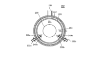
- FIG. 2 is a schematic block diagram of a vertical processing furnace of a substrate processing apparatus suitably used in an embodiment of the present invention, the processing furnace portion being a sectional view taken along the line AA of FIG.
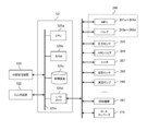
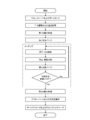
- FIG. 2 is a schematic block diagram of the controller of the substrate processing apparatus suitably used by one Embodiment of this invention, and is a figure which shows the control system of a controller with a block diagram. It is a flowchart which shows the substrate processing sequence of one Embodiment of this invention.
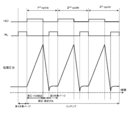
- FIG. 5 is a view extracting and showing a gas supply sequence and the like in a first hydrogen purge step and an etching step in FIG. 4.
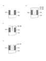
- A shows the surface structure of the wafer before forming the first Si film
- (b) shows the surface structure of the wafer after forming the first Si film
- (c) shows after etching a part of the first Si film
- FIG. 7D is an enlarged cross-sectional view showing the surface structure of the wafer after the second Si film is formed on the first Si film partially etched.
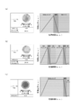
- (A) is a figure which shows the evaluation result (Example 1) of the uniformity of the etching amount of Si film in a wafer surface
- (b) is the evaluation result of the uniformity of the etching amount of Si film in a wafer surface
- (C) is a figure which shows the evaluation result (comparative example) of the uniformity of the etching amount of Si film
- the processing furnace 202 has a heater 207 as a heating mechanism (temperature adjustment unit).
- the heater 207 has a cylindrical shape, and is vertically installed by being supported by the holding plate.
- the heater 207 also functions as an activation mechanism (excitation unit) that thermally activates (excites) the gas.
- a reaction tube 203 is disposed concentrically with the heater 207.
- the reaction tube 203 is made of, for example, a heat resistant material such as quartz (SiO 2 ) or silicon carbide (SiC), and is formed in a cylindrical shape whose upper end is closed and whose lower end is open.
- a processing chamber 201 is formed in the hollow portion of the reaction tube 203.
- the processing chamber 201 is configured to be able to accommodate a wafer 200 as a substrate.
- nozzles 249a and 249b are provided so as to penetrate the lower side wall of the reaction tube 203.
- Gas supply pipes 232a and 232b are connected to the nozzles 249a and 249b, respectively.
- mass flow controllers (MFC) 241a and 241b which are flow controllers (flow control units) and valves 243a and 243b which are on-off valves are provided in this order from the upstream side of the gas flow.
- Gas supply pipes 232c and 232d are connected to the gas supply pipes 232a and 232b, respectively, downstream of the valves 243a and 243b.
- MFCs 241c and 241d and valves 243c and 243d are provided in this order from the upstream side of the gas flow.
- the nozzles 249 a and 249 b are provided in an annular space in plan view between the inner wall of the reaction tube 203 and the wafer 200, along the upper portion from the lower portion of the inner wall of the reaction tube 203. It is provided to rise upward in the loading direction. That is, the nozzles 249a and 249b are provided along the wafer array area in the area horizontally surrounding the wafer array area on the side of the wafer array area in which the wafers 200 are arrayed. Gas supply holes 250a and 250b for supplying gas are respectively provided on side surfaces of the nozzles 249a and 249b.
- the gas supply holes 250 a and 250 b are opened to face the center of the reaction tube 203, and can supply gas toward the wafer 200.
- a plurality of gas supply holes 250 a and 250 b are provided from the lower portion to the upper portion of the reaction tube 203.
- a silicon (Si) -containing gas is supplied from the gas supply pipe 232a into the processing chamber 201 through the MFC 241a, the valve 243a, and the nozzle 249a.
- a silicon hydride gas such as a monosilane (SiH 4 , abbreviated: MS) gas can be used.
- the etching gas is supplied from the gas supply pipe 232a into the processing chamber 201 via the MFC 241a, the valve 243a, and the nozzle 249a.
- hydrogen chloride (HCl) gas which is a gas containing halogen atoms and atoms other than halogen atoms, can be used as the etching gas.
- the dopant gas is supplied from the gas supply pipe 232 b into the processing chamber 201 through the MFC 241 b, the valve 243 b, and the nozzle 249 b.
- the dopant gas for example, phosphine (PH 3 , abbreviated as PH) gas containing phosphorus (P) as a dopant (impurity) can be used.
- hydrogen (H 2 ) gas as hydrogen (H) -containing gas and nitrogen (N 2 ) gas as inert gas are supplied by the MFCs 241c and 241d, valves 243c and 243d, and gas supply, respectively.
- the gas is supplied into the processing chamber 201 through the pipes 232a and 232b and the nozzles 249a and 249b.
- a source gas supply system and an etching gas supply system are mainly configured by the gas supply pipe 232a, the MFC 241a and the valve 243a.
- a dopant gas supply system is mainly configured by the gas supply pipe 232b, the MFC 241b, and the valve 243b.
- An H-containing gas supply system and an inert gas supply system are mainly configured by the gas supply pipes 232c and 232d, the MFCs 241c and 241d, and the valves 243c and 243d, respectively.
- any or all of the supply systems may be configured as an integrated supply system 248 in which the valves 243a to 243d, the MFCs 241a to 241d, and the like are integrated.
- the integrated supply system 248 is connected to each of the gas supply pipes 232a to 232d, and supplies various gases into the gas supply pipes 232a to 232d, that is, opens and closes the valves 243a to 243d or the MFCs 241a to 241d.
- the flow rate adjustment operation and the like are configured to be controlled by a controller 121 described later.
- the integrated supply system 248 is configured as an integrated or divided integrated unit, and can be attached to and detached from the gas supply pipes 232 a to 232 d etc. in units of integrated units. Maintenance, replacement, addition, and the like can be performed in units of integrated units.
- An exhaust pipe 231 for exhausting the atmosphere in the processing chamber 201 is connected to the lower side wall of the reaction pipe 203.
- the exhaust pipe 231 is provided with a pressure sensor 245 as a pressure detector (pressure detection unit) for detecting the pressure in the processing chamber 201 and an APC (Auto Pressure Controller) valve 244 as a pressure regulator (pressure adjustment unit).
- the vacuum pump 246 as an evacuation apparatus is connected.
- the APC valve 244 can perform vacuum evacuation and vacuum evacuation stop inside the processing chamber 201 by opening and closing the valve while operating the vacuum pump 246, and further, with the vacuum pump 246 operating,
- the pressure in the processing chamber 201 can be adjusted by adjusting the valve opening based on the pressure information detected by the pressure sensor 245.
- An exhaust system is mainly configured by the exhaust pipe 231, the pressure sensor 245, and the APC valve 244.
- the vacuum pump 246 may be included in the exhaust system.
- a seal cap 219 as a furnace port cover capable of airtightly closing the lower end opening of the reaction tube 203 is provided.
- the seal cap 219 is made of, for example, a metal material such as SUS, and is formed in a disk shape.
- an O-ring 220 is provided on the top surface of the seal cap 219 as a seal member that abuts on the lower end of the reaction tube 203.
- a rotation mechanism 267 for rotating a boat 217 described later is installed below the seal cap 219.
- the rotation shaft 255 of the rotation mechanism 267 is connected to the boat 217 through the seal cap 219.
- the rotation mechanism 267 is configured to rotate the wafer 200 by rotating the boat 217.
- the seal cap 219 is configured to be vertically lifted and lowered by a boat elevator 115 as a lift mechanism installed outside the reaction tube 203.
- the boat elevator 115 is configured as a transfer device (transfer mechanism) that carries the wafer 200 into and out of the processing chamber 201 by moving the seal cap 219 up and down.
- the boat 217 as a substrate support supports a plurality of, for example, 25 to 200 wafers 200 in a horizontal posture and vertically aligned with multiple centers aligned with one another, ie, It is configured to arrange at intervals.
- the boat 217 is made of, for example, a heat resistant material such as quartz or SiC.
- a heat insulating plate 218 made of a heat resistant material such as quartz or SiC is supported in multiple stages in a horizontal posture.
- a temperature sensor 263 as a temperature detector is installed in the reaction tube 203.
- the temperature sensor 263 is provided along the inner wall of the reaction tube 203.
- the controller 121 which is a control unit (control means), is configured as a computer including a central processing unit (CPU) 121a, a random access memory (RAM) 121b, a storage device 121c, and an I / O port 121d. It is done.
- the RAM 121b, the storage device 121c, and the I / O port 121d are configured to be able to exchange data with the CPU 121a via the internal bus 121e.
- An input / output device 122 configured as, for example, a touch panel or the like is connected to the controller 121.
- the storage device 121 c is configured by, for example, a flash memory, a hard disk drive (HDD), or the like.
- a control program for controlling the operation of the substrate processing apparatus, and a process recipe in which a procedure, conditions and the like of the substrate processing described later are stored are readably stored.
- the process recipe is a combination of processes so as to cause the controller 121 to execute each procedure in the substrate processing process described later and obtain a predetermined result, and functions as a program.
- the process recipe, the control program and the like are collectively referred to simply as a program.
- the process recipe is simply referred to as a recipe.
- the RAM 121 b is configured as a memory area (work area) in which programs and data read by the CPU 121 a are temporarily stored.
- the I / O port 121d is connected to the MFCs 241a to 241d, the valves 243a to 243d, the pressure sensor 245, the APC valve 244, the vacuum pump 246, the heater 207, the temperature sensor 263, the rotation mechanism 267, the boat elevator 115, etc. .
- the CPU 121a is configured to read out and execute the control program from the storage device 121c, and to read out the recipe from the storage device 121c in response to the input of the operation command from the input / output device 122 or the like.
- the CPU 121a adjusts the flow rates of various gases by the MFCs 241a to 241d, opens and closes the valves 243a to 243d, opens and closes the APC valve 244, and adjusts the pressure by the APC valve 244 based on the pressure sensor 245 in accordance with the contents of the read recipe. Operation, start and stop of vacuum pump 246, temperature adjustment operation of heater 207 based on temperature sensor 263, rotation and rotation speed adjustment of boat 217 by rotation mechanism 267, elevation operation of boat 217 by boat elevator 115, etc. Is configured.
- the controller 121 installs the above program stored in an external storage device (for example, a magnetic disk such as HDD, an optical disk such as CD, an optical magnetic disk such as MO, a semiconductor memory such as USB memory) 123 in a computer Can be configured by
- the storage device 121 c and the external storage device 123 are configured as computer readable recording media. Hereinafter, these are collectively referred to simply as recording media.
- recording medium when the term "recording medium" is used in the present specification, when only the storage device 121c is included, only the external storage device 123 may be included, or both of them may be included.
- the program may be provided to the computer using communication means such as the Internet or a dedicated line without using the external storage device 123.
- first Si film a first film
- second Si film a second film
- step of etching a part of the first Si film Supplying the HCl gas as the etching gas into the processing chamber 201 while raising the pressure in the processing chamber 201 with the wafer 200 having the first Si film formed on the surface housed in the processing chamber 201; In the state where supply of HCl gas into the processing chamber 201 is stopped, the pressure in the processing chamber 201 is lowered by exhausting the inside of the processing chamber 201; Perform a predetermined number of cycles including.
- wafer When the term “wafer” is used in the present specification, it may mean the wafer itself or a laminate of the wafer and a predetermined layer or film formed on the surface thereof.
- surface of wafer When the term “surface of wafer” is used in the present specification, it may mean the surface of the wafer itself or the surface of a predetermined layer or the like formed on the wafer.
- the phrase “forming a predetermined layer on the wafer” means that the predetermined layer is directly formed on the surface of the wafer itself, or a layer formed on the wafer, etc. It may mean forming a predetermined layer on top of.
- substrate in this specification is also synonymous with the use of the word "wafer”.
- a plurality of wafers 200 are loaded into the boat 217 (wafer charging). Thereafter, as shown in FIG. 1, the boat 217 supporting the plurality of wafers 200 is lifted by the boat elevator 115 and carried into the processing chamber 201 (boat loading). In this state, the seal cap 219 seals the lower end of the reaction tube 203 via the O-ring 220.
- the wafer 200 for example, a Si substrate made of single crystal Si, or a substrate having a single crystal Si film formed on the surface can be used.
- the surface of the wafer 200 is provided with a recess.
- the bottom of the recess is made of single crystal Si, and the side and top of the recess is an insulating film 200a such as a silicon oxide film (SiO film), a silicon nitride film (SiN film) or a silicon oxycarbonitride film (SiOCN film). It is composed of
- the surface of the wafer 200 is in a state in which the single crystal Si and the insulating film 200a are exposed.
- the inside of the processing chamber 201 is evacuated (reduced pressure exhaust) by the vacuum pump 246 so that the inside of the processing chamber 201, that is, the space in which the wafer 200 exists has a desired pressure (vacuum degree).
- the pressure in the processing chamber 201 is measured by the pressure sensor 245, and the APC valve 244 is feedback-controlled based on the measured pressure information.
- the wafer 207 in the processing chamber 201 is heated by the heater 207 so as to have a desired temperature.
- the degree of energization of the heater 207 is feedback-controlled based on the temperature information detected by the temperature sensor 263 so that the inside of the processing chamber 201 has a desired temperature distribution.
- the rotation of the wafer 200 by the rotation mechanism 267 is started.
- the operation of the vacuum pump 246 and the heating and rotation of the wafer 200 are both continued at least until the processing of the wafer 200 is completed.
- the first Si film By supplying the MS gas to the wafer 200, as shown in FIG. 6B, it is possible to form the first Si film so as to fill the inside of the recess.
- the surface side of the concave portion is blocked by the first Si film grown so as to overhang from the side portion and the upper portion of the concave portion.
- a non-embedded region extending in the depth region (direction) that is, a hollow portion such as a void or a seam may be formed in the recess.
- the hollow portion is generated by closing the surface side of the recess before the inside of the recess is completely filled with the first Si film, and the MS gas does not reach the inside of the recess and the growth of the first Si film in the recess stops. Do.
- the hollow portion is likely to be produced when the aspect ratio of the recess (the depth of the recess / the width of the recess) is increased, specifically, when the aspect ratio is 1 or more, for example, 20 or more, or 50 or more. Become. Also, as the aspect ratio increases, the hollow portion is more easily formed on the bottom side in the recess.
- Si grows amorphous (amorphous), poly (polycrystalline), or mixed crystal of amorphous and poly at least on the side and upper side of the recess. That is, the crystal structure of a portion of the first Si film grown so as to overhang at least from the side and top of the recess is amorphous, poly, or a mixed crystal of amorphous and poly.
- the valve 243 a is closed to stop the supply of the MS gas into the processing chamber 201.
- the supply of the MS gas may be stopped before the surface side of the concave portion is blocked by the first Si film, or may be stopped after it is completely blocked.
- the inside of the processing chamber 201 is evacuated, and the gas and the like remaining in the processing chamber 201 are removed from the inside of the processing chamber 201.
- the valves 243 c and 243 d are opened to supply N 2 gas into the processing chamber 201.
- the N 2 gas acts as a purge gas.
- MS gas supply flow rate 10 to 2000 sccm N 2 gas supply flow rate (each gas supply pipe): 0 to 10000 sccm Gas supply time: 20 to 400 minutes
- Processing temperature 450 to 550 ° C., preferably 450 to 530 ° C.
- Processing pressure 1 to 900 Pa Is illustrated.
- the processing temperature By setting the processing temperature to 530 ° C. or less, preferably less than 530 ° C., it becomes easy to make the crystal structure of the first Si film amorphous, thereby further enhancing the etching rate in the etching step described later. The productivity can be further improved.
- the crystallization temperature of Si is about 530 ° C.
- the crystal structure of the first Si film can be made amorphous by setting the treatment temperature to less than 530 ° C., and the treatment temperature is set to exceed 530 ° C.
- the crystal structure of the first Si film can be made to be poly, and by setting the processing temperature to about 530 ° C., the crystal structure of the first Si film can be made to be a mixed crystal of amorphous and poly.
- n H 2n + 2 n Can be a silicon hydride gas represented by an integer of 1 or more.
- MCS dichlorosilane
- DCS dichlorosilane
- TCS trichlorosilane
- SiCl 3 ) 4 tetrachlorosilane
- chlorosilane-based gas such as STC gas, hexachlorodisilane (Si 2 Cl
- rare gases such as Ar gas, He gas, Ne gas and Xe gas can be used in addition to N 2 gas. This point is the same in each step described later.
- H 2 gas is supplied to the wafer 200 in the processing chamber 201, that is, the first Si film formed on the wafer 200.
- the valves 243c and 243d are opened to flow the H 2 gas into the gas supply pipes 232c and 232d.
- the flow rate of the H 2 gas is adjusted by the MFCs 241 c and 241 d, and is supplied into the processing chamber 201 through the gas supply pipes 232 a and 232 b and the nozzles 249 a and 249 b and exhausted from the exhaust pipe 231.
- H 2 gas is supplied to the wafer 200.
- valves 243 c and 243 d are closed to stop the supply of the H 2 gas into the processing chamber 201.
- the APC valve 244 kept open, the inside of the processing chamber 201 is exhausted by the vacuum pump 246.
- the N 2 gas may be supplied into the processing chamber 201.
- the N 2 gas acts as a purge gas.
- H 2 gas supply flow rate 500 to 3000 sccm
- Gas supply time 20 to 400 minutes
- Processing pressure 1 to 1000 Pa Is illustrated.
- the other processing conditions such as the processing temperature are the same as the processing conditions in the first Si film forming step.
- Step-up / HCl supply step In this step, HCl gas is supplied to the wafer 200 in the processing chamber 201, that is, the first Si film formed on the wafer 200 and subjected to the first hydrogen purge step. Specifically, the opening and closing control of the valves 243a, 243c, and 243d is performed in the same procedure as the opening and closing control of the valves 243a, 243c, and 243d in the first Si film forming step.
- the flow rate of HCl gas is adjusted by the MFC 241 a, supplied into the processing chamber 201 via the nozzle 249 a, and exhausted from the exhaust pipe 231. At this time, HCl gas is supplied to the wafer 200.
- part of the first Si film formed on the wafer 200 can be etched.
- the upper part of the hollow part formed under the part can be opened to expose the inner wall (side wall or bottom part) of the hollow part.
- the amount of HCl gas supplied to the inside of the hollow portion gradually decreases from the surface side toward the bottom side. Therefore, as shown in FIG.
- the longitudinal cross-sectional shape of the exposed hollow portion approaches a V shape or an inverted trapezoidal shape in which the opening width gradually increases from the bottom side toward the surface side.
- the pressure in the processing chamber 201 is set to a relatively low predetermined pressure (starting pressure).
- starting pressure a relatively low predetermined pressure
- the flow rate (diffusion rate) of HCl gas supplied into the processing chamber 201 can be increased, and the entire area in the processing chamber 201, that is, the surface of the wafer 200 can be obtained. It is possible to supply HCl gas in a uniform amount to the whole area of As a result, the above-mentioned etching process can be started at uniform timing and progress at an equal rate over the entire surface of the wafer 200.
- the opening degree of the APC valve 244 is adjusted to keep increasing the pressure in the processing chamber 201.
- the HCl gas is supplied into the processing chamber 201 while maintaining the pressure in the processing chamber 201 at a constant pressure, or the HCl gas is supplied into the processing chamber 201 while the pressure in the processing chamber 201 is lowered. Step is not implemented.
- the pressure in the processing chamber 201 can be prevented from being maintained at a constant high pressure. For example, HCl gas stagnates in the central portion of the wafer 200. It becomes possible to prevent that.
- the etching rate of the first Si film can be gradually increased (varied), which makes it possible to improve the efficiency of the etching process.
- the pressure in the processing chamber 201 is excessively increased or maintained at a constant high pressure, the flow velocity of HCl gas in the processing chamber 201 is reduced, and, for example, the HCl gas stagnates in the central portion of the wafer 200. May.
- the etching amount of the first Si film in the central portion of the wafer 200 becomes larger than the etching amount of the first Si film in the peripheral portion of the wafer 200, etc.
- the uniformity of the etching amount may be reduced.
- HCl gas supply flow rate 100 to 10000 sccm Gas supply time: 10 to 60 minutes Start pressure (processing pressure at the start of this step): 1 to 1000 Pa End pressure (processing pressure at the end of this step): 28000 to 32000 Pa The average boost rate: 400 to 1100 Pa / min is exemplified.
- the other processing conditions such as the processing temperature are the same as the processing conditions in the first Si film forming step.
- the processing pressure (a pressure above the start pressure and a pressure below the end pressure) in this step continues to increase at least, retention of HCl gas at the central portion of the wafer 200 can be prevented. It is a pressure that makes it possible to maintain in-plane uniformity.
- the end pressure in this step is the maximum processing chamber pressure in the etching step, and is a pressure larger than the maximum processing chamber pressure in the above-described first Si film forming step and the second Si film forming step described later.
- the processing temperature in this step is a temperature at which the amorphous state of the first Si film is maintained, ie, the first Si film, when the first Si film formed on the wafer 200 in the first Si film forming step is in an amorphous state.
- the temperature at which the crystallization of the first Si film is avoided is a temperature at which the first Si film is not crystallized (polycrystallized), and is also a temperature at which the first Si film is not epilated (monocrystallized). This temperature is also a temperature at which the in-plane uniformity of the etching amount of the first Si film can be further increased because the crystallization of the first Si film is avoided.
- Step-down, evacuation step When the pressure raising / HCl supply step is completed, the valve 243 a is closed, and with the supply of HCl gas into the processing chamber 201 stopped, the APC valve 244 is fully opened (full open). Thus, the inside of the processing chamber 201 is evacuated (vacuated), and the pressure in the processing chamber 201 is lowered.
- the pressure change amount (pressure change rate, pressure reduction rate) per unit time in this step is made larger than the pressure change amount (pressure change rate, pressure increase rate) per unit time in the pressure increase / HCl supply step.
- the average step-down rate during the execution of this step is a rate larger than the average step-up rate in the above-described step-up / HCl supply step, and is, for example, in the range of 5000 to 7000 Pa / min.
- the implementation time of this step is shorter than the implementation time of the pressurization / HCl supply step, and is, for example, in the range of 5 to 10 minutes.
- a predetermined number of cycles (n times, n is an integer of 1 or more) are performed non-simultaneously, that is, without synchronizing the three steps described above.
- FIG. 5 shows an example in which this cycle is performed three times.
- the aspect ratio of the recess formed on the surface of the wafer 200 is, for example, 20 or more by performing the cycle a plurality of times, for example, about 3 to 10 times in this way, that is, the hollow portion is the bottom in the recess Even when it is formed on the side, it is possible to expose the hollow portion and to easily process the vertical cross-sectional shape of the exposed hollow portion into a V-shape or the like.
- the inside of the recess can be filled with the Si film more reliably.
- the first Si film formed on the wafer 200 in the processing chamber 201 is processed by the same processing procedure as the first Si film forming step.
- An MS gas is supplied to the partially etched first Si film.
- the supply time of the MS gas is, for example, in the range of 10 to 300 minutes.
- the other processing conditions are the same as the processing conditions in the first Si film forming step.
- a second Si film is formed on the wafer 200, that is, on the surface of the first Si film partially etched. Can.
- the hollow portion of the first Si film is exposed with the top open, and the longitudinal cross-sectional shape is from the bottom side to the surface side It is processed into V shape etc. where opening width becomes large gradually as it goes to.
- the second Si film does not grow so as to overhang from the side or the like of the open hollow portion. That is, the surface side of the open hollow portion is not closed and the MS gas does not reach the inside of the hollow portion.
- the hollow portion is not formed in the second Si film, and the inside of the recess provided on the surface of the wafer 200 is completely, ie, void free and seamless, by the first Si film and the second Si film.
- the crystal structure of the second Si film is amorphous, poly, or a mixed crystal thereof.
- valve 243 a is closed to stop the supply of the MS gas into the processing chamber 201. Then, according to the same processing procedure as the first Si film forming step, the inside of the processing chamber 201 is evacuated and the gas and the like remaining in the processing chamber 201 are removed from the inside of the processing chamber 201.
- N 2 gas is supplied from the gas supply pipes 232 c and 232 d into the processing chamber 201 and exhausted from the exhaust pipe 231.
- the inside of the processing chamber 201 is purged, and gas, reaction by-products and the like remaining in the processing chamber 201 are removed from the inside of the processing chamber 201 (after purge).
- the atmosphere in the processing chamber 201 is replaced with the inert gas (inert gas substitution), and the pressure in the processing chamber 201 is returned to normal pressure (atmospheric pressure recovery).
- the etching step the upper portion of the hollow portion of the first Si film is opened by performing the cycle including the pressure raising / HCl supply step and the pressure lowering / evacuating step a predetermined number of times, and the longitudinal sectional shape is It becomes possible to process it into a V-shape or the like. Thereby, in the second Si film forming step, the inside of the recess can be filled with the Si film more reliably.
- (G) extending the execution time of the pressure rising / HCl supply step by making the pressure rising rate in the pressure rising / HCl supplying step smaller than the pressure lowering rate in the pressure reducing / evacuating step; It can be made longer than time. That is, it is possible to secure a long time for the HCl gas supplied into the processing chamber 201 to be diffused at a high flow rate without staying on the surface of the wafer 200. This makes it possible to improve the uniformity of the etching process of the first Si film in the surface of the wafer 200.
- the etching temperature when chlorine (Cl 2 ) gas is used as the etching gas, it is necessary to set the etching temperature to, for example, about 350 ° C. in order to etch the first Si film. In this case, it is necessary to reduce the temperature in the processing chamber 201 by 100 ° C. or more and provide a temperature lowering step for waiting until the temperature is stabilized between the first Si film forming step and the etching step. In addition, it is necessary to increase the temperature in the processing chamber 201 by 100 ° C. or more between the etching step and the second Si film forming step, and provide a temperature rising step for waiting until the temperature is stabilized.
- the etching step is performed at a temperature at which the amorphous state of the first Si film is maintained, thereby crystallizing the first Si film. It becomes possible to avoid. Thereby, in the etching step, it is possible to maintain a high etching rate of the first Si film, and to improve the productivity of the substrate processing. In addition, it is possible to avoid local crystallization of a part of the first Si film, and it is possible to suppress the formation of irregularities on the surface of the first Si film after etching.
- the surface of the first Si film formed on the wafer 200 can be hydrogen-terminated to clean the entire surface. This makes it possible to improve the uniformity of the etching process of the first Si film in the surface of the wafer 200.
- a pressure maintaining step may be performed to supply HCl gas into the processing chamber 201 while maintaining the pressure in the processing chamber 201 at a constant pressure.
- the pressure maintenance step may be performed, for example, before starting the pressure boosting / HCl supply step, or may be performed during the execution of the pressure boosting / HCl supply step, and after the completion of the pressure boosting / HCl supply step. It may be performed before starting the evacuation step.
- the execution time of the pressure maintenance step is higher than the etching rate of the first Si film at the central portion of the wafer 200 than the etching rate of the first Si film at the peripheral portion of the wafer 200. It is time until it becomes large. Also in this modification, the same effect as the above-mentioned substrate processing sequence shown in FIG. 4, FIG. 5 and the like can be obtained.
- the PH gas may be supplied to the wafer 200 together (simultaneously) with the MS gas.
- the first Si film is a Si film doped with P as a dopant.
- the supply flow rate of the PH gas is appropriately determined according to the specifications of the device formed on the wafer 200, etc., but can be, for example, within a range of 0.1 to 500 sccm. Also in this modification, the same effect as the above-mentioned substrate processing sequence shown in FIG. 4, FIG. 5 and the like can be obtained.
- the above-mentioned technical problem (the decrease in the uniformity of the etching process) due to the retention of the HCl gas is particularly noticeable when the first Si film is a non-doped Si film. Therefore, the technical significance of the etching process described in the present embodiment is particularly significant when forming a non-doped Si film on the wafer 200.
- the above cycle may be performed only once. If the aspect ratio of the recess formed on the surface of the wafer 200 is not so large, it is possible to process the vertical cross-sectional shape of the exposed hollow portion into a V-shape or the like even by performing the above cycle once. Become. In this case, the substrate processing procedure can be simplified, and the processing time can be shortened.
- the present invention It is not limited to this aspect.
- the first Si film forming step and the step group subsequent to the etching step can be performed (ex-situ) in different processing chambers.
- a series of steps leading to the etching step and a second Si film forming step can be performed ex-situ.
- the first and second Si film forming steps and the etching step can be performed ex-situ.
- each step can be performed ex-situ.
- the wafer 200 will not be exposed to the atmosphere during the process, and the process can be performed consistently while keeping the wafer 200 in a clean atmosphere, which is stable. It becomes possible to perform a film formation process.
- the recipe used for substrate processing be individually prepared according to the processing content, and stored in the storage device 121 c via the telecommunication line or the external storage device 123. Then, when the substrate processing is started, it is preferable that the CPU 121a appropriately select an appropriate recipe from among the plurality of recipes stored in the storage device 121c in accordance with the content of the substrate processing.
- the burden on the operator can be reduced, and processing can be quickly started while avoiding an operation error.
- the above-described recipe is not limited to the case of creating a new one, and may be prepared, for example, by changing an existing recipe already installed in the substrate processing apparatus.
- the changed recipe may be installed in the substrate processing apparatus via the telecommunication line or the recording medium recording the recipe.
- the existing recipe that has already been installed in the substrate processing apparatus may be directly changed by operating the input / output device 122 provided in the existing substrate processing apparatus.
- the example which forms a film using the batch type substrate processing apparatus which processes a plurality of substrates at once was explained.
- the present invention is not limited to the above-described embodiment, and can be suitably applied to, for example, the case where a film is formed using a sheet-fed substrate processing apparatus that processes one or several substrates at a time.
- the example of forming the film using the substrate processing apparatus having the hot wall type processing furnace has been described.
- the present invention is not limited to the above-described embodiment, and can be suitably applied to the case of forming a film using a substrate processing apparatus having a cold wall type processing furnace.
- film formation can be performed under the same processing procedure and processing conditions as those of the above-described embodiment and modification, and the same effects as these can be obtained.
- processing procedure and processing conditions at this time can be, for example, the same as the processing procedure and processing conditions of the above-described embodiment.
- Example 1 using the substrate processing apparatus shown in FIG. 1, the Si film formed on the surface of the wafer was etched by the same processing procedure as the etching step in the above embodiment.
- the step of supplying HCl gas into the processing chamber while maintaining the pressure in the processing chamber at a constant pressure was not performed.
- the number of cycles performed in the etching step was one.
- Other processing conditions were set as predetermined conditions within the processing condition range described in the above-described embodiment.
- Example 2 using the substrate processing apparatus shown in FIG. 1, the Si film formed on the surface of the wafer was etched by the same processing procedure as the etching step in the above embodiment.
- the step of supplying HCl gas into the processing chamber while maintaining the pressure in the processing chamber at a constant pressure was not performed.
- the number of cycles performed in the etching step was two.
- Other processing conditions were the same as the processing conditions of Example 1.
- the pressure in the processing chamber in which the wafer is stored is increased, and when the pressure in the processing chamber reaches a pressure within the range of 28000 to 32000 Pa, the pressure is made constant.
- the Si film formed on the surface of the wafer was etched by supplying HCl gas into the processing chamber while maintaining it.
- Other processing conditions were the same as the processing conditions of Example 1.
- FIGS. 7 (a) to 7 (c) are diagrams showing measurement results and the like of Examples 1 and 2 and a comparative example. The smaller the WiW, the higher the uniformity of the etching amount in the wafer surface.
- the WiW in Examples 1 and 2 is smaller than the WiW in the comparative example. That is, it can be seen that the etching method (the method of the above-described embodiment) employed in Examples 1 and 2 has better uniformity of the etching amount in the wafer plane than the etching method employed in the comparative example. . Further, according to FIGS. 7A and 7B, the WiWs of Examples 1 and 2 are substantially the same, and even if the number of cycles in the etching step is increased or decreased, uniformity of the etching amount in the wafer surface is obtained. It can be seen that there is no effect on In addition, since the average etching amount of the second embodiment is about twice the average etching amount of the first embodiment, it is possible to accurately control the average etching amount by adjusting the number of cycles. I understand.
Landscapes
- Chemical & Material Sciences (AREA)
- Engineering & Computer Science (AREA)
- Mechanical Engineering (AREA)
- Chemical Kinetics & Catalysis (AREA)
- General Chemical & Material Sciences (AREA)
- Materials Engineering (AREA)
- Metallurgy (AREA)
- Organic Chemistry (AREA)
- Inorganic Chemistry (AREA)
- Physics & Mathematics (AREA)
- Plasma & Fusion (AREA)
- Chemical Vapour Deposition (AREA)
- Drying Of Semiconductors (AREA)
Abstract
Description
表面に膜が形成された基板を処理室内に収容した状態で、前記処理室内の圧力を上昇させつつ、前記処理室内へエッチングガスを供給する工程と、
前記処理室内への前記エッチングガスの供給を停止した状態で、前記処理室内を排気することで、前記処理室内の圧力を降下させる工程と、
を含むサイクルを所定回数行うことで、前記基板の表面に形成された膜の一部をエッチングする技術が提供される。
以下、本発明の一実施形態について、図1~図5、図6(a)~図6(d)を用いて説明する。
図1に示すように、処理炉202は加熱機構(温度調整部)としてのヒータ207を有する。ヒータ207は円筒形状であり、保持板に支持されることにより垂直に据え付けられている。ヒータ207は、ガスを熱で活性化(励起)させる活性化機構(励起部)としても機能する。
上述の基板処理装置を用い、半導体装置の製造工程の一工程として、基板としてのウエハ200上にシリコン膜(Si膜)を形成するシーケンス例について、主に、図4、図5、図6(a)~図6(d)を用いて説明する。以下の説明において、基板処理装置を構成する各部の動作はコントローラ121により制御される。
ウエハ200の表面に設けられた凹部内を埋め込むように第1膜(第1Si膜)を形成するステップと、
ウエハ200の表面に形成された第1Si膜の一部をエッチングするステップと、
一部がエッチングされた第1Si膜上に、さらに第2膜(第2Si膜)を形成するステップと、
を行うことで、凹部内を第1Si膜および第2Si膜で埋め込む。
表面に第1Si膜が形成されたウエハ200を処理室201内に収容した状態で、処理室201内の圧力を上昇させつつ、処理室201内へエッチングガスとしてHClガスを供給するステップと、
処理室201内へのHClガスの供給を停止した状態で、処理室201内を排気することで、処理室201内の圧力を降下させるステップと、
を含むサイクルを所定回数行う。
複数枚のウエハ200がボート217に装填(ウエハチャージ)される。その後、図1に示すように、複数枚のウエハ200を支持したボート217は、ボートエレベータ115によって持ち上げられて処理室201内へ搬入(ボートロード)される。この状態で、シールキャップ219は、Oリング220を介して反応管203の下端をシールした状態となる。
処理室201内、すなわち、ウエハ200が存在する空間が所望の圧力(真空度)となるように、真空ポンプ246によって処理室201内が真空排気(減圧排気)される。この際、処理室201内の圧力は圧力センサ245で測定され、この測定された圧力情報に基づきAPCバルブ244がフィードバック制御される。また、処理室201内のウエハ200が所望の温度となるように、ヒータ207によって加熱される。この際、処理室201内が所望の温度分布となるように、温度センサ263が検出した温度情報に基づきヒータ207への通電具合がフィードバック制御される。また、回転機構267によるウエハ200の回転を開始する。真空ポンプ246の稼働、ウエハ200の加熱および回転は、いずれも、少なくともウエハ200に対する処理が終了するまでの間は継続して行われる。
その後、処理室201内のウエハ200に対し、MSガスを供給する。このステップでは、バルブ243aを開き、ガス供給管232a内へMSガスを流す。MSガスは、MFC241aにより流量調整され、ノズル249aを介して処理室201内へ供給され、排気管231から排気される。このとき、ウエハ200に対してMSガスが供給される。このときバルブ243c,243dを開き、ガス供給管232c,232d内へN2ガスを流すようにしてもよい。N2ガスは、MFC241c,241dにより流量調整され、ノズル249a,249bを介して処理室201内へ供給される。
MSガス供給流量:10~2000sccm
N2ガス供給流量(各ガス供給管):0~10000sccm
ガス供給時間:20~400分
処理温度:450~550℃、好ましくは450~530℃
処理圧力:1~900Pa
が例示される。
第1Si膜形成ステップが終了した後、処理室201内のウエハ200、すなわち、ウエハ200上に形成された第1Si膜に対してH2ガスを供給する。具体的には、バルブ243c,243dを開き、ガス供給管232c,232d内へH2ガスを流す。H2ガスは、MFC241c,241dにより流量調整され、ガス供給管232a,232b、ノズル249a,249bを介して処理室201内へ供給され、排気管231から排気される。このとき、ウエハ200に対してH2ガスが供給される。ウエハ200に対してH2ガスを供給することで、ウエハ200上に形成された第1Si膜の表面を水素終端させ、その表面全域を清浄化させることが可能となる。
H2ガス供給流量:500~3000sccm
ガス供給時間:20~400分
処理圧力:1~1000Pa
が例示される。処理温度等の他の処理条件は、第1Si膜形成ステップにおける処理条件と同様とする。
第1水素パージステップが終了した後、後述する昇圧・HCl供給ステップ、降圧・真空排気ステップ、第2水素パージステップを順に行う。
このステップでは、処理室201内のウエハ200、すなわち、ウエハ200上に形成され、第1水素パージステップがなされた第1Si膜に対してHClガスを供給する。具体的には、バルブ243a,243c,243dの開閉制御を、第1Si膜形成ステップにおけるバルブ243a,243c,243dの開閉制御と同様の手順で行う。HClガスは、MFC241aにより流量調整され、ノズル249aを介して処理室201内へ供給され、排気管231から排気される。このとき、ウエハ200に対してHClガスが供給される。
HClガス供給流量:100~10000sccm
ガス供給時間:10~60分
開始圧力(本ステップ開始時の処理圧力):1~1000Pa
終了圧力(本ステップ終了時の処理圧力):28000~32000Pa
平均昇圧レート:400~1100Pa/分
が例示される。処理温度等の他の処理条件は、第1Si膜形成ステップにおける処理条件と同様とする。
昇圧・HCl供給ステップが終了したら、バルブ243aを閉じ、処理室201内へのHClガスの供給を停止した状態で、APCバルブ244を全開(フルオープン)とする。これにより、処理室201内を真空排気(真空引き)し、処理室201内の圧力を降下させる。
処理室201内の圧力が所定の真空排気圧力に到達したら、第1水素パージステップと同様の処理手順により、処理室201内へH2ガスを供給する。これにより、処理室201内に残留するHClやCl等を処理室201内から効率的に排除することができる。その後、第1水素パージステップと同様の処理手順により、処理室201内を排気する。H2ガスの供給時間は、例えば5~10分の範囲内の時間とする。他の処理条件は、第1水素パージステップの処理条件と同様とする。
上述した3つのステップを非同時に、すなわち、同期させることなく行うサイクルを所定回数(n回、nは1以上の整数)行う。図5は、このサイクルを3回実施する例を示している。このようにサイクルを複数回、例えば3~10回程度実施することにより、ウエハ200の表面に形成された凹部のアスペクト比が例えば20以上となるような場合、すなわち、中空部が凹部内における底部側に形成されるような場合であっても、中空部を露出させ、さらに、露出した中空部の縦断面形状をV字形状等へと加工することが容易に行えるようになる。結果として、後述する第2Si膜形成ステップにおいて、凹部の内部のSi膜による埋め込みを、より確実に行えるようになる。
エッチングステップが終了した後、第1Si膜形成ステップと同様の処理手順により、処理室201内のウエハ200、すなわち、ウエハ200上に形成され、エッチング処理が施された後の第1Si膜、すなわち、一部がエッチングされた第1Si膜に対し、MSガスを供給する。MSガスの供給時間は、例えば10~300分の範囲内の時間とする。他の処理条件は、第1Si膜形成ステップにおける処理条件と同様とする。
第2Si膜形成ステップが終了した後、ガス供給管232c,232dのそれぞれからN2ガスを処理室201内へ供給し、排気管231から排気する。これにより、処理室201内がパージされ、処理室201内に残留するガスや反応副生成物等が処理室201内から除去される(アフターパージ)。その後、処理室201内の雰囲気が不活性ガスに置換され(不活性ガス置換)、処理室201内の圧力が常圧に復帰される(大気圧復帰)。
その後、ボートエレベータ115によりシールキャップ219が下降され、反応管203の下端が開口されるとともに、処理済のウエハ200が、ボート217に支持された状態で、反応管203の下端から反応管203の外部に搬出(ボートアンロード)される。処理済のウエハ200は、反応管203の外部に搬出された後、ボート217より取り出される(ウエハディスチャージ)。
本実施形態によれば、以下に示す1つ又は複数の効果が得られる。
本実施形態は、以下の変形例のように変更することができる。また、これらの変形例は、任意に組み合わせることができる。特に説明がない限り、各変形例の各ステップにおける処理手順、処理条件は、上述の基板処理シーケンスの各ステップにおける処理手順、処理条件と同様とする。
エッチングステップにおいて、比較的短時間であれば、処理室201内の圧力を一定圧力に維持しつつ処理室201内へHClガスを供給する圧力維持ステップを実施するようにしてもよい。圧力維持ステップは、例えば、昇圧・HCl供給ステップを開始する前に行ってもよく、昇圧・HCl供給ステップの実施期間中に行ってもよく、昇圧・HCl供給ステップの終了後であって降圧・真空排気ステップを開始する前に行ってもよい。圧力維持ステップを実施する際は、その実施時間を、圧力維持ステップを開始してから、ウエハ200の中央部における第1Si膜のエッチングレートがウエハ200の周縁部における第1Si膜のエッチングレートよりも大きくなる前までの時間とする。本変形例においても、図4、図5等に示す上述の基板処理シーケンスと同様の効果が得られる。
第1Si膜形成ステップにおいては、ウエハ200に対してMSガスと一緒に(同時に)PHガスを供給するようにしてもよい。この場合、第1Si膜は、ドーパントとしてのPがドープされたSi膜となる。PHガスの供給流量は、ウエハ200上に形成するデバイスの仕様等によって適宜決定されるが、例えば0.1~500sccmの範囲内の流量とすることができる。本変形例においても、図4、図5等に示す上述の基板処理シーケンスと同様の効果が得られる。但し、上述したHClガスの滞留による技術的課題(エッチング処理の均一性低下)は、第1Si膜がノンドープSi膜である場合に特に顕著に生じることとなる。そのため、本実施形態で示したエッチング処理の技術的意義は、ウエハ200上にノンドープSi膜を形成する際に特に大きなものとなる。
エッチングステップにおいては、上述のサイクルを1回のみ行うようにしてもよい。ウエハ200の表面に形成された凹部のアスペクト比がさほど大きくない場合、上述のサイクルを1回行うことによっても、露出した中空部の縦断面形状をV字形状等へと加工することが可能となる。この場合、基板処理の手順を簡素化させ、また、処理時間を短縮させることが可能となる。
第1水素パージステップおよび第2水素パージステップのうち、いずれかのステップの実施を省略してもよい。また、これら両方のステップの実施をそれぞれ省略してもよい。これらの場合、基板処理の手順を簡素化させたり、処理時間を短縮させたりすることが可能となる。ただし、エッチング処理の均一性をより向上させたり、エッチング処理の効率をより向上させたりするには、これらのステップを省略することなく実施するほうが好ましい。
以上、本発明の実施形態を具体的に説明した。但し、本発明は上述の実施形態に限定されるものではなく、その要旨を逸脱しない範囲で種々変更可能である。
Claims (18)
- 表面に膜が形成された基板を処理室内に収容した状態で、前記処理室内の圧力を上昇させつつ、前記処理室内へエッチングガスを供給する工程と、
前記処理室内への前記エッチングガスの供給を停止した状態で、前記処理室内を排気することで、前記処理室内の圧力を降下させる工程と、
を含むサイクルを所定回数行うことで、前記基板の表面に形成された膜の一部をエッチングする工程を有する半導体装置の製造方法。 - 前記処理室内の圧力を降下させる工程における単位時間あたりの圧力変化量を、前記エッチングガスを供給する工程における単位時間あたりの圧力変化量よりも大きくする請求項1に記載の半導体装置の製造方法。
- 前記処理室内の圧力を降下させる工程の実施時間を、前記エッチングガスを供給する工程の実施時間よりも短くする請求項1に記載の半導体装置の製造方法。
- 前記膜の一部をエッチングする工程では、
前記処理室内の圧力を一定圧力に維持しつつ前記処理室内へ前記エッチングガスを供給する工程を不実施とするか、もしくは、
前記処理室内の圧力を一定圧力に維持しつつ前記処理室内へ前記エッチングガスを供給する工程を実施する場合は、その実施時間を、前記基板の中央部における前記膜のエッチングレートが前記基板の周縁部における前記膜のエッチングレートよりも大きくなる前までの時間とする請求項1に記載の半導体装置の製造方法。 - 前記膜の一部をエッチングする工程では、前記処理室内の圧力を降下させつつ前記処理室内へ前記エッチングガスを供給する工程を不実施とする請求項1に記載の半導体装置の製造方法。
- 前記膜の一部をエッチングする工程では、前記処理室内へ前記エッチングガスを供給している間は、前記膜のエッチングレートを上昇させ続ける請求項1に記載の半導体装置の製造方法。
- 前記サイクルは、さらに、前記処理室内を水素含有ガスでパージする工程を含む請求項1に記載の半導体装置の製造方法。
- 前記膜の一部をエッチングする工程では、前記サイクルを複数回繰り返す請求項1に記載の半導体装置の製造方法。
- 前記膜の一部をエッチングする工程を実施する前に、前記基板の表面に設けられた凹部内を埋め込むように前記膜を形成する工程を、さらに有する請求項1に記載の半導体装置の製造方法。
- 前記膜の一部をエッチングする工程を実施した後に、一部がエッチングされた前記膜上に、さらに膜を形成する工程を、さらに有する請求項1に記載の半導体装置の製造方法。
- 前記膜を形成する工程、前記膜の一部をエッチングする工程、および、前記さらに膜を形成する工程を、同一の前記処理室内で行う請求項10に記載の半導体装置の製造方法。
- 前記膜を形成する工程、前記膜の一部をエッチングする工程、および、前記さらに膜を形成する工程を、同一温度下で行う請求項10に記載の半導体装置の製造方法。
- 前記膜を形成する工程、前記膜の一部をエッチングする工程、および、前記さらに膜を形成する工程を、前記膜の結晶化温度以下の温度下で行う請求項10に記載の半導体装置の製造方法。
- 前記膜の一部をエッチングする工程における最大処理室内圧力を、前記膜を形成する工程および前記さらに膜を形成する工程のそれぞれにおける最大処理室内圧力よりも大きくする請求項11に記載の半導体装置の製造方法。
- 前記膜を形成する工程および前記さらに膜を形成する工程では、前記膜として、ノンドープシリコン膜を形成する請求項10に記載の半導体装置の製造方法。
- 前記膜を形成する工程および前記さらに膜を形成する工程では、前記膜として、ドーパントがドープされたシリコン膜を形成する請求項10に記載の半導体装置の製造方法。
- 基板に対する処理が行われる処理室と、
前記処理室内へエッチングガスを供給するエッチングガス供給系と、
前記処理室内の圧力を調整する圧力調整部と、
前記処理室内を排気する排気系と、
表面に膜が形成された基板を前記処理室内に収容した状態で、前記処理室内の圧力を上昇させつつ、前記処理室内へ前記エッチングガスを供給する処理と、前記処理室内への前記エッチングガスの供給を停止した状態で、前記処理室内を排気することで、前記処理室内の圧力を降下させる処理と、を含むサイクルを所定回数行うことで、前記基板の表面に形成された膜の一部をエッチングする処理を行わせるように、前記エッチングガス供給系、前記圧力調整部、および前記排気系を制御するよう構成される制御部と、
を有する基板処理装置。 - 基板処理装置の処理室内に、表面に膜が形成された基板を収容した状態で、前記処理室内の圧力を上昇させつつ、前記処理室内へエッチングガスを供給する手順と、
前記処理室内への前記エッチングガスの供給を停止した状態で、前記処理室内を排気することで、前記処理室内の圧力を降下させる手順と、
を含むサイクルを所定回数行うことで、前記基板の表面に形成された膜の一部をエッチングする手順をコンピュータによって前記基板処理装置に実行させるプログラム。
Priority Applications (6)
| Application Number | Priority Date | Filing Date | Title |
|---|---|---|---|
| KR1020227042861A KR20230004882A (ko) | 2017-08-14 | 2018-05-25 | 반도체 장치의 제조 방법, 기판 처리 장치 및 프로그램 |
| CN201880043858.2A CN110832621B (zh) | 2017-08-14 | 2018-05-25 | 半导体器件的制造方法、衬底处理装置及记录介质 |
| KR1020207004301A KR20200029015A (ko) | 2017-08-14 | 2018-05-25 | 반도체 장치의 제조 방법, 기판 처리 장치 및 프로그램 |
| KR1020257025189A KR20250117737A (ko) | 2017-08-14 | 2018-05-25 | 기판 처리 방법, 기판 처리 장치, 프로그램 및 반도체 장치의 제조 방법 |
| JP2019536426A JPWO2019035258A1 (ja) | 2017-08-14 | 2018-05-25 | 半導体装置の製造方法、基板処理装置およびプログラム |
| US16/790,294 US11581200B2 (en) | 2017-08-14 | 2020-02-13 | Method of manufacturing semiconductor device, substrate processing apparatus, and recording medium |
Applications Claiming Priority (2)
| Application Number | Priority Date | Filing Date | Title |
|---|---|---|---|
| JP2017-156541 | 2017-08-14 | ||
| JP2017156541 | 2017-08-14 |
Related Child Applications (1)
| Application Number | Title | Priority Date | Filing Date |
|---|---|---|---|
| US16/790,294 Continuation US11581200B2 (en) | 2017-08-14 | 2020-02-13 | Method of manufacturing semiconductor device, substrate processing apparatus, and recording medium |
Publications (1)
| Publication Number | Publication Date |
|---|---|
| WO2019035258A1 true WO2019035258A1 (ja) | 2019-02-21 |
Family
ID=65362816
Family Applications (1)
| Application Number | Title | Priority Date | Filing Date |
|---|---|---|---|
| PCT/JP2018/020187 Ceased WO2019035258A1 (ja) | 2017-08-14 | 2018-05-25 | 半導体装置の製造方法、基板処理装置およびプログラム |
Country Status (5)
| Country | Link |
|---|---|
| US (1) | US11581200B2 (ja) |
| JP (1) | JPWO2019035258A1 (ja) |
| KR (3) | KR20250117737A (ja) |
| CN (1) | CN110832621B (ja) |
| WO (1) | WO2019035258A1 (ja) |
Citations (5)
| Publication number | Priority date | Publication date | Assignee | Title |
|---|---|---|---|---|
| JPS63304631A (ja) * | 1987-06-05 | 1988-12-12 | Hitachi Ltd | 光励起ドライエツチング方法およびその装置 |
| JP2002353205A (ja) * | 2000-08-28 | 2002-12-06 | Mitsubishi Electric Corp | 半導体装置の製造方法およびそれに用いられるウェハ処理装置並びに半導体装置 |
| JP2005150332A (ja) * | 2003-11-14 | 2005-06-09 | Sony Corp | エッチング方法 |
| JP2012004542A (ja) * | 2010-05-20 | 2012-01-05 | Tokyo Electron Ltd | シリコン膜の形成方法およびその形成装置 |
| JP2012146741A (ja) * | 2011-01-07 | 2012-08-02 | Hitachi Kokusai Electric Inc | 半導体装置の製造方法および基板処理装置 |
Family Cites Families (7)
| Publication number | Priority date | Publication date | Assignee | Title |
|---|---|---|---|---|
| JP3485081B2 (ja) * | 1999-10-28 | 2004-01-13 | 株式会社デンソー | 半導体基板の製造方法 |
| JP2003218037A (ja) | 2002-01-21 | 2003-07-31 | Denso Corp | 半導体基板の製造方法 |
| JP3918565B2 (ja) | 2002-01-21 | 2007-05-23 | 株式会社デンソー | 半導体装置の製造方法 |
| JP4652282B2 (ja) * | 2006-05-30 | 2011-03-16 | 三菱電機株式会社 | シリコン基板の表面処理方法および太陽電池セルの製造方法 |
| JP5773954B2 (ja) * | 2012-07-02 | 2015-09-02 | 三菱電機株式会社 | ガラス基板エッチング装置およびガラス基板エッチング方法 |
| JP6055637B2 (ja) | 2012-09-20 | 2016-12-27 | 株式会社日立国際電気 | クリーニング方法、半導体装置の製造方法、基板処理装置及びプログラム |
| JP7203515B2 (ja) * | 2017-06-06 | 2023-01-13 | アプライド マテリアルズ インコーポレイテッド | 連続した堆積-エッチング-処理方法を使用した酸化ケイ素及び窒化ケイ素のボトムアップ成長 |
-
2018
- 2018-05-25 KR KR1020257025189A patent/KR20250117737A/ko active Pending
- 2018-05-25 WO PCT/JP2018/020187 patent/WO2019035258A1/ja not_active Ceased
- 2018-05-25 KR KR1020227042861A patent/KR20230004882A/ko not_active Ceased
- 2018-05-25 CN CN201880043858.2A patent/CN110832621B/zh active Active
- 2018-05-25 KR KR1020207004301A patent/KR20200029015A/ko not_active Ceased
- 2018-05-25 JP JP2019536426A patent/JPWO2019035258A1/ja active Pending
-
2020
- 2020-02-13 US US16/790,294 patent/US11581200B2/en active Active
Patent Citations (5)
| Publication number | Priority date | Publication date | Assignee | Title |
|---|---|---|---|---|
| JPS63304631A (ja) * | 1987-06-05 | 1988-12-12 | Hitachi Ltd | 光励起ドライエツチング方法およびその装置 |
| JP2002353205A (ja) * | 2000-08-28 | 2002-12-06 | Mitsubishi Electric Corp | 半導体装置の製造方法およびそれに用いられるウェハ処理装置並びに半導体装置 |
| JP2005150332A (ja) * | 2003-11-14 | 2005-06-09 | Sony Corp | エッチング方法 |
| JP2012004542A (ja) * | 2010-05-20 | 2012-01-05 | Tokyo Electron Ltd | シリコン膜の形成方法およびその形成装置 |
| JP2012146741A (ja) * | 2011-01-07 | 2012-08-02 | Hitachi Kokusai Electric Inc | 半導体装置の製造方法および基板処理装置 |
Also Published As
| Publication number | Publication date |
|---|---|
| US11581200B2 (en) | 2023-02-14 |
| CN110832621B (zh) | 2024-04-09 |
| US20200185237A1 (en) | 2020-06-11 |
| JPWO2019035258A1 (ja) | 2020-03-26 |
| CN110832621A (zh) | 2020-02-21 |
| KR20250117737A (ko) | 2025-08-05 |
| KR20230004882A (ko) | 2023-01-06 |
| KR20200029015A (ko) | 2020-03-17 |
Similar Documents
| Publication | Publication Date | Title |
|---|---|---|
| US10199219B2 (en) | Method of manufacturing semiconductor device, substrate processing apparatus, and recording medium | |
| US11043392B2 (en) | Method of manufacturing semiconductor device, substrate processing apparatus and recording medium | |
| JP6606476B2 (ja) | 半導体装置の製造方法、基板処理装置およびプログラム | |
| US10134584B2 (en) | Method of manufacturing semiconductor device, substrate processing apparatus, and recording medium | |
| US11075114B2 (en) | Method of manufacturing semiconductor device, substrate processing apparatus, and recording medium | |
| US11047048B2 (en) | Method of manufacturing semiconductor device, substrate processing apparatus, and recording medium | |
| US11164744B2 (en) | Method of manufacturing semiconductor device, substrate processing apparatus, and recording medium | |
| KR102726911B1 (ko) | 기판 처리 방법, 반도체 장치의 제조 방법, 기판 처리 장치, 및 프로그램 | |
| WO2019003662A1 (ja) | 半導体装置の製造方法、基板処理装置およびプログラム | |
| US10529560B2 (en) | Method of manufacturing semiconductor device, substrate processing apparatus and recording medium | |
| JP7524333B2 (ja) | 半導体装置の製造方法、プログラム、基板処理装置及び基板処理方法 | |
| WO2019035258A1 (ja) | 半導体装置の製造方法、基板処理装置およびプログラム | |
| JP7644739B2 (ja) | 基板処理方法、半導体装置の製造方法、プログラム、および基板処理装置 | |
| JP2021064807A (ja) | 半導体装置の製造方法、基板処理装置およびプログラム | |
| WO2022176155A1 (ja) | 半導体装置の製造方法、基板処理装置、およびプログラム |
Legal Events
| Date | Code | Title | Description |
|---|---|---|---|
| 121 | Ep: the epo has been informed by wipo that ep was designated in this application |
Ref document number: 18846791 Country of ref document: EP Kind code of ref document: A1 |
|
| ENP | Entry into the national phase |
Ref document number: 2019536426 Country of ref document: JP Kind code of ref document: A |
|
| ENP | Entry into the national phase |
Ref document number: 20207004301 Country of ref document: KR Kind code of ref document: A |
|
| NENP | Non-entry into the national phase |
Ref country code: DE |
|
| 122 | Ep: pct application non-entry in european phase |
Ref document number: 18846791 Country of ref document: EP Kind code of ref document: A1 |
|
| WWR | Wipo information: refused in national office |
Ref document number: 1020227042861 Country of ref document: KR |
|
| WWD | Wipo information: divisional of initial pct application |
Ref document number: 1020257025189 Country of ref document: KR |
|
| WWP | Wipo information: published in national office |
Ref document number: 1020257025189 Country of ref document: KR |