WO2019016887A1 - Dispositif d'imagerie d'images tomographiques - Google Patents
Dispositif d'imagerie d'images tomographiques Download PDFInfo
- Publication number
- WO2019016887A1 WO2019016887A1 PCT/JP2017/026091 JP2017026091W WO2019016887A1 WO 2019016887 A1 WO2019016887 A1 WO 2019016887A1 JP 2017026091 W JP2017026091 W JP 2017026091W WO 2019016887 A1 WO2019016887 A1 WO 2019016887A1
- Authority
- WO
- WIPO (PCT)
- Prior art keywords
- light
- signal
- optical path
- reflected
- path length
- Prior art date
Links
Images


Classifications
-
- G—PHYSICS
- G01—MEASURING; TESTING
- G01B—MEASURING LENGTH, THICKNESS OR SIMILAR LINEAR DIMENSIONS; MEASURING ANGLES; MEASURING AREAS; MEASURING IRREGULARITIES OF SURFACES OR CONTOURS
- G01B9/00—Measuring instruments characterised by the use of optical techniques
- G01B9/02—Interferometers
- G01B9/0209—Low-coherence interferometers
- G01B9/02091—Tomographic interferometers, e.g. based on optical coherence
-
- A—HUMAN NECESSITIES
- A61—MEDICAL OR VETERINARY SCIENCE; HYGIENE
- A61B—DIAGNOSIS; SURGERY; IDENTIFICATION
- A61B5/00—Measuring for diagnostic purposes; Identification of persons
- A61B5/0059—Measuring for diagnostic purposes; Identification of persons using light, e.g. diagnosis by transillumination, diascopy, fluorescence
- A61B5/0062—Arrangements for scanning
- A61B5/0066—Optical coherence imaging
-
- G—PHYSICS
- G01—MEASURING; TESTING
- G01B—MEASURING LENGTH, THICKNESS OR SIMILAR LINEAR DIMENSIONS; MEASURING ANGLES; MEASURING AREAS; MEASURING IRREGULARITIES OF SURFACES OR CONTOURS
- G01B11/00—Measuring arrangements characterised by the use of optical techniques
- G01B11/24—Measuring arrangements characterised by the use of optical techniques for measuring contours or curvatures
- G01B11/2441—Measuring arrangements characterised by the use of optical techniques for measuring contours or curvatures using interferometry
-
- G—PHYSICS
- G01—MEASURING; TESTING
- G01B—MEASURING LENGTH, THICKNESS OR SIMILAR LINEAR DIMENSIONS; MEASURING ANGLES; MEASURING AREAS; MEASURING IRREGULARITIES OF SURFACES OR CONTOURS
- G01B9/00—Measuring instruments characterised by the use of optical techniques
- G01B9/02—Interferometers
- G01B9/02001—Interferometers characterised by controlling or generating intrinsic radiation properties
- G01B9/02002—Interferometers characterised by controlling or generating intrinsic radiation properties using two or more frequencies
- G01B9/02003—Interferometers characterised by controlling or generating intrinsic radiation properties using two or more frequencies using beat frequencies
-
- G—PHYSICS
- G01—MEASURING; TESTING
- G01B—MEASURING LENGTH, THICKNESS OR SIMILAR LINEAR DIMENSIONS; MEASURING ANGLES; MEASURING AREAS; MEASURING IRREGULARITIES OF SURFACES OR CONTOURS
- G01B9/00—Measuring instruments characterised by the use of optical techniques
- G01B9/02—Interferometers
- G01B9/02001—Interferometers characterised by controlling or generating intrinsic radiation properties
- G01B9/0201—Interferometers characterised by controlling or generating intrinsic radiation properties using temporal phase variation
-
- G—PHYSICS
- G01—MEASURING; TESTING
- G01B—MEASURING LENGTH, THICKNESS OR SIMILAR LINEAR DIMENSIONS; MEASURING ANGLES; MEASURING AREAS; MEASURING IRREGULARITIES OF SURFACES OR CONTOURS
- G01B9/00—Measuring instruments characterised by the use of optical techniques
- G01B9/02—Interferometers
- G01B9/02001—Interferometers characterised by controlling or generating intrinsic radiation properties
- G01B9/02012—Interferometers characterised by controlling or generating intrinsic radiation properties using temporal intensity variation
-
- G—PHYSICS
- G01—MEASURING; TESTING
- G01N—INVESTIGATING OR ANALYSING MATERIALS BY DETERMINING THEIR CHEMICAL OR PHYSICAL PROPERTIES
- G01N21/00—Investigating or analysing materials by the use of optical means, i.e. using sub-millimetre waves, infrared, visible or ultraviolet light
- G01N21/17—Systems in which incident light is modified in accordance with the properties of the material investigated
- G01N21/47—Scattering, i.e. diffuse reflection
- G01N21/4795—Scattering, i.e. diffuse reflection spatially resolved investigating of object in scattering medium
-
- A—HUMAN NECESSITIES
- A61—MEDICAL OR VETERINARY SCIENCE; HYGIENE
- A61B—DIAGNOSIS; SURGERY; IDENTIFICATION
- A61B2562/00—Details of sensors; Constructional details of sensor housings or probes; Accessories for sensors
- A61B2562/02—Details of sensors specially adapted for in-vivo measurements
- A61B2562/0233—Special features of optical sensors or probes classified in A61B5/00
-
- G—PHYSICS
- G01—MEASURING; TESTING
- G01N—INVESTIGATING OR ANALYSING MATERIALS BY DETERMINING THEIR CHEMICAL OR PHYSICAL PROPERTIES
- G01N21/00—Investigating or analysing materials by the use of optical means, i.e. using sub-millimetre waves, infrared, visible or ultraviolet light
- G01N21/17—Systems in which incident light is modified in accordance with the properties of the material investigated
- G01N2021/178—Methods for obtaining spatial resolution of the property being measured
- G01N2021/1785—Three dimensional
- G01N2021/1787—Tomographic, i.e. computerised reconstruction from projective measurements
-
- G—PHYSICS
- G01—MEASURING; TESTING
- G01N—INVESTIGATING OR ANALYSING MATERIALS BY DETERMINING THEIR CHEMICAL OR PHYSICAL PROPERTIES
- G01N21/00—Investigating or analysing materials by the use of optical means, i.e. using sub-millimetre waves, infrared, visible or ultraviolet light
- G01N21/17—Systems in which incident light is modified in accordance with the properties of the material investigated
- G01N21/47—Scattering, i.e. diffuse reflection
- G01N21/4795—Scattering, i.e. diffuse reflection spatially resolved investigating of object in scattering medium
- G01N2021/4797—Scattering, i.e. diffuse reflection spatially resolved investigating of object in scattering medium time resolved, e.g. analysis of ballistic photons
Definitions
- the present invention relates to a tomographic imaging apparatus that captures a tomographic image of an object, and more particularly to a tomographic imaging apparatus that uses a code having a repeating characteristic such as an M-sequence code in a predetermined cycle.
- Patent Document 1 Japanese Patent Application Laid-Open No. 2011-117789 discloses a wide band light pulse generation unit for generating a wide band light pulse having a predetermined wavelength band, and a wide band light pulse by dividing the wide band light pulse.
- a light pulse generating a plurality of narrow band light pulses narrower than a wavelength band, and delaying each of the narrow band light pulses for different times and then combining them to generate a light pulse train composed of a plurality of light pulses having different center wavelengths.
- a demultiplexing delay multiplexing unit an optical branching unit for branching the optical pulse train into a measurement optical pulse train and a reference optical pulse train, and irradiating the measurement optical pulse train on a measurement target, and the measurement optical pulse train being backward according to the measurement target
- An optical pulse irradiation / acquisition unit for acquiring a backscattered light pulse train generated by scattering, a combination of the reference light pulse train and the backscattered light pulse train, Measurement data corresponding to the light intensity according to the optical coupler forming the row, the light pulse intensity measurement unit for measuring the light intensity of each light pulse of the combined light pulse train, and the wave number of each light pulse of the combined light pulse train
- An optical coherence tomography apparatus is described that has a tomogram deriving unit that derives a tomogram of the measurement object on the basis of the measurement data obtained by Fourier-transforming and Fourier-transforming.
- Patent Document 2 Japanese Patent Laid-Open No. 2006-184284 describes a light source of an optical interference tomography apparatus having means capable of switching the wave number in a step-like manner.
- pulsed light is irradiated to a measurement object to capture scattered light in the measurement object.
- the difference in attenuation within the pulse width is large, that is, the signal of the scattered light on the light incident side is strong, and the signal of the scattered light on the back side is weak. For this reason, it becomes difficult to capture a clear tomographic image over a predetermined depth.
- An object of the present invention is to provide a tomographic imaging apparatus capable of obtaining a tomographic image with a high signal-to-noise ratio with high resolution and in a short measurement time and also in the deep part of the measurement object.
- a light source generating coherent light
- a modulator modulating the light generated by the light source with a code having an autocorrelation characteristic
- a frequency of the light modulated by the modulator Optical path length of the frequency shifter to be converted, the reference reflector for reflecting the light passing through the frequency shifter, the light modulated by the modulator, and the light reflected by the reference reflector via the frequency shifter
- a measurement system detection unit that includes an optical path length change unit that changes the light intensity; a first light detector that detects light; and a first AD converter that converts an output signal of the first light detector into a digital signal;
- a reference system detection unit including a second light detector for detecting light and a second AD converter for converting an output signal of the second light detector into a digital signal; and the measurement system detection unit outputs Signal and the reference
- the first light detector includes a demodulator that combines the signal output from the detection unit and an analyzer that
- the light reflected by the reference reflector through the frequency shifter and the light whose optical path length has been changed by the optical path length changing unit is input, and is reflected by the reference reflector to the second photodetector.
- the light and the light reflected by the reference reflector via the frequency shifter are input, and the analysis unit analyzes the signal output from the demodulator to calculate the position of the reflection point of the measurement object It is characterized by
- tomographic images with high resolution and high signal-to-noise ratio can be captured at high speed even in the deep part of the measurement object.
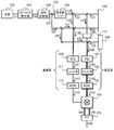
- FIG. 1 is a view showing the arrangement of a tomographic imaging apparatus according to the first embodiment of the present invention.
- the tomographic imaging apparatus includes a light source 100, an optical pulse generator 101, a waveform shaper 102, a frequency shifter 104, an optical path length changing unit 114, light detectors 107 and 108, filters 110 and 111, and AD conversion. And a demodulator 109 and a Fourier transformer 115.
- the light source 100 is a light source that generates coherent continuous light 121, and for example, a laser light source can be used. Further, the light emitted from the light source 100 is controlled so that the wavelength changes in a predetermined frequency range in a predetermined wavelength range. The bandwidth (range of frequency change) of the frequency of light emitted from the light source 100 corresponds to the resolution of the image of the measurement object 106.
- the light pulse generator 101 converts light (continuous light) generated by the light source 100 into pulse light 122 having a predetermined width and a predetermined shape.
- the optical pulse generator 101 is configured by an optical comb generator, and can excite the optical comb generator with a predetermined microwave or millimeter wave high frequency signal to obtain femtosecond pulse light at a constant interval. For example, if it controls by a signal of 25 GHz, as shown in FIG. 2, femtosecond pulse light with an interval of 40 picoseconds (25 Gbps) can be generated.
- the duty ratio of the femtosecond light pulse signal 122 generated by the light pulse generator 101 is very small, the measurement target range is narrowed, and the influence of scattered light from other than the optical axis direction can be reduced. In addition, the amount of change in attenuation within the measurement range can be reduced, and a high quality image can be obtained. This improves the signal-to-noise ratio of the reflected light at the measurement object 106.
- the duty ratio of the light pulse signal 122 is too small, the peak energy of the light is limited for safety reasons, the average energy of the light decreases, and the depth detectable when the object of measurement 106 is irradiated. Becomes shallow, or the number of times of integration of the reflected pulse increases and the measurement time to the measurement target point becomes long.
- the waveform shaper 102 shapes the optical pulse signal 122 output from the optical pulse generator 101, which repeats at a fixed time interval, into a pulse waveform having a predetermined time width, and further, the necessary number of pulses is required on the time axis Output the signal copied to the upper point.
- the same envelope waveform as that of the pulse waveform is used to generate a ⁇ -phase light pulse whose phase is inverted, and a signal obtained by duplicating the necessary number at the necessary position is output.
- the waveform shaper 102 generates an M-sequence code of symbol length 2 n-1 and outputs a signal 123.
- the waveform shaper 102 spectrally resolves the input signal 122 with a spectroscope, adjusts the phase and amplitude for each spectrum using a phase space modulator, and performs spectrum synthesis again to obtain a predetermined M sequence. Generate and output a code.
- the M-sequence code signal thus fixed is repeatedly generated and output.
- modulation can be performed at high speed, and a pulse corresponding to one bit of the M-sequence code can be set to a predetermined width, so that the measurement target range can be set to the predetermined range.
- the predetermined measurement range varies depending on the attenuation characteristics and scattering characteristics of the light to be measured, it is desirable that a sufficient signal-to-noise ratio be obtained over the entire predetermined range. In actual observation of a living body, it is required that the measurement range determined by one bit pulse is about 0.5 mm or less.
- the spatial phase modulator exemplified in the present embodiment outputs a signal 123 obtained by shaping the optical pulse signal copied by the waveform shaper 102 into a predetermined waveform such as a Chebyshev shape.
- a Chebyshev shaped waveform By using a Chebyshev shaped waveform, the side lobes in the frequency domain can be reduced, and interference between adjacent waveforms can be reduced, so that the resolution of the measurement object 106 can be improved.
- the waveform of the output signal of the spatial phase modulator may be a waveform having a sufficiently small side lobe even if it is not of the Chebyshev type.
- the illustrated waveform former 102 generates 127 pulses (a code of 127 bits) in 40 picoseconds, and generates an optical signal 123 modulated at 3.2 THz.
- the pulse generated by the spatial phase modulator from one light pulse, that is, the symbol length of the M-sequence code may not be 127 bits, and may be longer 255 bits or shorter 63 bits.
- waveform shaper 102 is configured using Arrayed-Waveguide Grating (AWG)
- AWG Arrayed-Waveguide Grating
- modulation can be performed at high speed as in the case of using a spatial phase modulator.
- the phase and amplitude can be controlled statically in the spectrum in the frequency domain to produce a fixed M-sequence two-phase modulated signal.
- adjacent pulses are separated, and the level may be zero between pulses, or the side lobes may be connected, and the level may not be zero between pulses.
- the signal 123 output from the waveform shaper 102 is branched into a signal 124 and a signal 129, and the signal 129 is input to the frequency shifter 104.
- the signal 124 is further branched into a signal 125 and a signal 127, and the signal 127 is reflected by the reference reflector 105 to become a signal 128, and the traveling direction is changed to be led to the light detector 108.
- the signal 125 is irradiated to the measurement object 106, reflected and scattered by the measurement object 106, and guided to the light detector 107 as a signal 126.
- the reflected light 126 from the measurement object 106 includes information of reflection points in a finite section in the measurement object 106.
- the reference reflector does not necessarily have to be a reflector, and may have a function of synchronizing the signal 130 and the signal 127 and returning the signal 131 and the signal 128 while maintaining the same optical path length. For example, by changing the external electric field, the effective length can be changed at high speed by changing the external electric field.
- the frequency shifter 104 converts the frequency of the input signal 128 and outputs a signal 130.
- the signals whose frequencies are converted by the frequency shifter 104 are synthesized by the photodetectors 107 and 108, and the frequency difference signals 140 and 141 are detected as the beat of the frequency shift amount (see FIG. 8A). Therefore, the frequency shift amount is preferably a frequency (for example, 100 MHz) that can be easily processed as an electrical signal after the photodetectors 107 and 108.
- the signal 130 output from the frequency shifter 104 is reflected by the reference reflector 105 to be a signal 131, and a part thereof is branched to be a signal 133 which is led to the light detector 107.
- the signal 133 becomes an optical signal in which light beams having different optical path lengths (that is, different wavefronts) travel in parallel via the optical path length changing unit 114 and is guided to the light detector 107. Further, a signal 132 in which a part of the reflected signal 130 is branched is led to the light detector 108.
- An optical signal to which is added is input. If the two signals input to the light detector 108 are correlated, the frequency difference signal 141 of the two signals is output. Since the two signals input to the light detector 108 are reflected by the same reference reflector 105 and guided to the light detector 108, the light path length is the same, and since the M-sequence code is always correlated, the light detector From 108, a frequency difference signal 141 of the two signals is output.
- the two signals input to the light detector 107 are not correlated, only the noise and the DC signal which are spread by the spectrum of the ultrafast M-sequence signal can be detected (see FIG. 8C).
- the demodulator 109 complex (IQ) demodulates the frequency difference signal 144 of the measurement system generated from the reflected light of the measurement object 106, using the AD-converted frequency difference signal 145 of the reference system as a reference signal. Although one demodulator 109 is provided in FIG.
- the Fourier transformer 115 functions as an analysis unit that analyzes the position of the reflection point, and Fourier-transforms the information of the reflection point obtained by the demodulator 109, that is, the frequency domain spectrum, to obtain the position of the reflection point. Specifically, by performing discrete Fourier transform (DFT) or Fourier series expansion, the position of the reflection point and the intensity of the reflected light at the position can be known. When performing discrete Fourier transform, it is preferable to further interpolate.
- DFT discrete Fourier transform
- Fourier series expansion the position of the reflection point and the intensity of the reflected light at the position can be known.
- the configuration of the optical path length changing unit 114 will be described.
- the optical path length changing unit 114 a mirror in which mirror surfaces are formed in a step shape, an optical path including fibers having different effective lengths, a mirror having a moving function, or the like can be adopted. Each mechanism will be described below.
- FIG. 3 is a diagram showing the concept of the light detector 107 and the optical path length changing unit 114. As shown in FIG. 3
- each detection element 1071 of the light detector 107 The light 126 reflected by the measurement object 106 and the light 133 reflected by the reference reflector 105 are introduced to each detection element (for example, photodiode) 1071 of the light detector 107.
- the optical path lengths of the reflected light 126 to the respective detection elements 1071 are illustrated differently, but in fact, the optical path lengths from the measurement object 106 to the respective detection elements 1071 are the same.
- the light detector 108 has the same configuration as the light detector 107, but light is introduced without passing through the optical path length changing unit 114.
- the light 133 reflected by the reference reflector 105 includes light components having different optical path lengths, and the optical path lengths of the light incident on the detection elements 1071 are different.
- the optical path length to the left detection element 1071 is short, and the optical path length to the right detection element 1071 is long.
- the difference in the optical path length to each detection element 1071 is set to 1 bit or less of the M-sequence code, and the auto-correlation of the M-sequence code is obtained in a specific detection element 1071. Do not get correlation. By doing this, it is possible to extract reflected light (with a specific optical path length range) from a specific range in the depth direction of the measurement object 106.
- the difference in optical path length to each detection element 1071 may be changed according to the waveform of the M-sequence code. For example, even when the pulse waveforms of the M-sequence code are shifted by a half cycle, even if the pulse waveforms overlap, autocorrelation between the codes is obtained, and a frequency difference signal of a size corresponding to the degree of overlap is obtained (FIG. B) see). On the other hand, when the pulse waveforms do not overlap in the state where they are shifted by a half cycle of the pulse waveform of the M-sequence code, the autocorrelation between the codes can not be obtained, and a frequency difference signal can not be obtained (see FIG. 8C). For this reason, it is preferable to increase the difference in optical path length when the overlap of pulse waveforms is small, and to reduce the difference in optical path length when the overlap of pulse waveforms is large.
- each detection element 1071 of the light detector 107 light having a different optical path length reflected by the measurement object 106, that is, the light detector 107 is light of light reflected at different depths of the measurement object 106.
- the intensity can be detected.
- the AD converter 112 converts the input analog signal 142 into a digital signal 144, and inputs the digital signal 144 into the IQ demodulator 109.
- the AD converter 113 converts the input analog signal 143 into a digital signal 145, and inputs the digital signal 145 to the IQ demodulator 109.
- the IQ demodulator 109 demodulates the signal 144 including the component of the reflected light from the object to be measured 106, using the signal 145 including only the component of the reflected light from the reference reflector 105 as a local oscillation signal. Then, from the IQ demodulator 109, a signal corresponding to the intensity of the reflected light from the depth (the position corresponding to the optical path length) of the measurement object 106 is obtained.
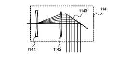
- FIG. 4 is a view showing a specific configuration example of the optical path length changing unit 114. As shown in FIG. 4
- the optical path length changing unit 114 has a mirror 1143 having a mirror surface formed in a step-like shape, as shown in FIG.
- the light introduced into the optical path length changing unit 114 is diffused by the concave lens 1141, becomes parallel light by the convex lens 1142, and is reflected by the mirror 1143. Since the mirror 1143 has a mirror surface formed in a step shape, light reflected at each step is output with different optical path lengths.
- the difference in the optical path length of one mirror surface is determined by the size of the lateral step of the mirror surface shown in FIG.
- the light emitted from the optical path length changing unit 114 is output so as to be equal to the pitch of the detection elements 1071 of the light detector 107.
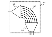
- FIG. 5 is a view showing another configuration of the optical path length changing unit 114. As shown in FIG.
- the optical path length changing unit 114 shown in FIG. 5 changes the optical path length using optical fibers 1147 having different lengths. Specifically, the light input to the optical path length changing unit 114 is diffused by the slab waveguide 1145 and is led out to a plurality of optical fibers 1147 having different lengths. The light propagated through the optical fibers 1147 is collected by the slab waveguide 1146 so as to be equal to the pitch of the detection elements 1071 of the light detector 107, and is output from the optical path length changing unit 114.
- the lengths of the optical fibers 1147 are made different, but the lengths of some or all of the optical fibers 1147 are equalized, and an electric field is applied to the optical fibers 1147 May control the propagation speed of
- optical path length changing unit 114 may move the mirror to change the optical path length.
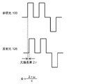
- FIG. 6 is a diagram showing a method of determining the reflection position and reflectance of the inside of the measurement object 106 from the signal 140 output from the light detector 107.
- the M-sequence code included in the reference light 133 reflected by the reference reflector 105 and the reflected light 126 reflected by the measurement object 106 is represented on the time axis.
- the reflected light 126 includes light reflected at a plurality of positions inside the measurement object 106, for convenience of explanation, the reflected light will be described using reflected light from one point.
- the reference light 133 and the reflected light 126 originally have the same signal but the position of the reflection point differs by r (that is, the optical path length is 2r).
- the signal is out of phase.
- a signal 100 MHz in this embodiment
- a frequency difference of light which is a carrier wave on which the M-sequence code is superimposed is output.
- the reference light 132 and the reference light 128 originally have the same signal, and the position (optical path length) of the reflection point is the same. Therefore, when the reference light 132 and the reflected light 128 are added in the light detector 107, a signal (100 MHz in this embodiment) of the frequency difference of light which is a carrier wave on which the M-sequence code is superimposed is output. Ru.
- the frequency difference signal of the reference system and the frequency difference signal of the measurement system are shifted in phase by ⁇ .
- One detection element 1071 of the light detector 107 extracts light incident on the light detector 107 at a specific timing by the autocorrelation characteristic of the M-sequence code. Since the light source 100 changes the wavelength and outputs light, a plurality of signals having different amplitudes and phases at multiple frequencies can be obtained. Since the amplitude is determined by the reflectance at the reflection point inside the measurement object 106 and the phase is determined by the optical path difference, the reflectance at each reflection point is analyzed by collecting and analyzing a plurality of sets of data of the amplitude and the phase. calculate.
- the irradiation light irradiated to the measurement object 106 is a transmission signal x ( ⁇ , t), and the reflection light reflected and scattered by the measurement object 106 is a reception signal y ( ⁇ , t).
- the transmission signal x ( ⁇ , t) is expressed by equation (1).
- f (t) is defined as a function represented by Formula (2) as a function representing a pulse waveform of the M-sequence code.
- the transmission signal pulse is expressed by equation (3).
- the reflection point of the measurement object 106 is separated from the reflection point of the reference reflector 105 by a distance r.
- the reflection point position of the reference reflector 105 is represented by (C ⁇ td) / 2
- the position of the reflection point of the measurement object 106 is represented by r + (C ⁇ td) / 2.
- the correlation S (t) is represented by the equations (5) and (6).
- the range of r is determined from the condition of equation (7), and the integration range of equation (6) is determined to be finite.
- integration is performed for t.
- Equation (12) is the bit length of the M-sequence code.
- a (r) can be represented by a Fourier series.
- ⁇ is defined by equation (13) and a (r) is defined by equation (14)
- the correlation S (n, ⁇ ) can be expressed by equation (15).
- Equation (18) exp [ ⁇ j ⁇ ⁇ S ⁇ ( ⁇ 2 r / C)] S is CT. Therefore, the FS coefficient of a (r) is obtained. Therefore, ⁇ S is expressed by Equations (16) and (17), and exp [ ⁇ j ⁇ ⁇ S ( ⁇ 2 r / C)] is expressed by Equation (18).
- Equation (21) the reflectance A (r) can be obtained by Equation (21) as a function of the distance.
- FIG. 7 is a view showing an observation range CT of a reflection point by autocorrelation
- FIG. 8 is a view showing a signal output from the light detector.
- the light reflected by the reflecting reflector 105 at the position B in the figure is input to the light detector 107 with an optical path length ABC.
- the light reflected by the measurement object 106 is input to the light detector 107 at an optical path length ADE.
- the optical path lengths are completely equal, as shown in FIG. 7A, the correlation is taken over all the symbol lengths of the M-sequence code, and as shown in FIG. A signal 140 is obtained.
- the tomographic imaging apparatus for measuring the depth direction of one point is described using the photodetector 107 in which the detection elements 1071 are arranged in one dimension (linearly).
- a two-dimensional tomographic image including the depth direction can be obtained by using the light sources 107 arranged linearly in a line and using the light detector 107 in which the detection elements 1071 are arranged two-dimensionally (planarly).
- the photodetector 107 in which the light sources 100 are arranged in a plane and the detection elements 1071 are arranged in a three-dimensional (three-dimensional) or two-dimensional (planar) array three-dimensional including the depth direction Tomographic images of
- FIG. 9 is a diagram showing simulation results of the measurement range.
- the reflectivity 900 of the object to be measured 106 is shown as a function of depth. Note that the reflectance 900 used in the simulation has already taken into consideration the attenuation of the light of the measurement object 106 due to the propagation of light, and the reflectance at the back is lowered.
- a line 901 shows a simulation of the imaging result by the tomographic imaging apparatus of the first embodiment, and a line 902 shows a simulation of the imaging result by the conventional tomographic imaging apparatus.
- a range 903 indicated by a broken line is a range where autocorrelation can be obtained by the M-sequence code, and in the tomographic imaging apparatus of the first embodiment, the reflectance of the measurement object 106 in this range is a function of depth Obtained as In addition, since a strong correlation is obtained in the center of the range shown by the broken line, the reflectance has a large value, and the reflectance becomes a smaller value as it goes to both sides. In order to know the correct reflectance, correction by the strength of correlation is necessary.
- the range shown in FIG. 3 is used to move the range 903 where autocorrelation can be obtained by sequentially switching the difference in optical path length, and the tomographic range in a wide range in the depth direction. You can take pictures.
- the reflection from the back of the measurement object 106 is weak, and is buried in noise at a certain point, making it impossible to measure the reflected light from a deeper point.
- a detailed image can be obtained within a narrow measurement range by using the autocorrelation characteristic of the M-sequence code.
- reference beams having different optical path lengths it is possible to change the range in which the autocorrelation characteristic of the M-sequence code can be obtained, and to capture a wide range of tomographic images.
- FIG. 10 is a view showing the arrangement of a tomographic imaging apparatus according to the second embodiment of the present invention.
- the tomographic imaging apparatus includes a light source 100, an optical pulse generator 101, a modulator 103, a frequency shifter 104, an optical path length changing unit 114, photodetectors 107 and 108, filters 110 and 111, and an AD converter. 112, 113, a demodulator 109 and a Fourier transformer 115.
- the waveform shaper 102 is not provided, and the configuration of the modulator 103 is different from that of the first embodiment.
- the same reference numerals are given to the same components as the above-described embodiment, and the description thereof will be omitted.
- the modulator 103 of the second embodiment phase modulates the signal 122 output from the optical pulse generator 101 using an M-sequence code, and outputs a signal 123.
- the modulator 103 is configured by an LN modulator.
- the LN modulator has a characteristic of outputting light in the state where no voltage is applied and not outputting light in the state where no voltage is applied, using the refractive index change due to the Pockels effect of LiNbO3 crystal.
- FIG. 11 is a diagram showing an example of light output from the modulator 103 in the tomographic imaging apparatus of the second embodiment.
- the optical pulse generator 101 controls the amplitude of the light (continuous light) emitted by the light source 100 with, for example, a signal of 25 GHz to generate a pulsed optical signal with an interval of 40 microseconds.
- Generate 122 controls the amplitude of the light (continuous light) emitted by the light source 100 with, for example, a signal of 25 GHz to generate a pulsed optical signal with an interval of 40 microseconds.
- the modulator 103 phase-modulates the signal 122 output from the optical pulse generator 101 using an M-sequence code, and outputs a signal 123.
- the modulator 103 is configured by an LN modulator.
- the frequency of the signal input to the modulator 103 is low, and the M-sequence code is modulated at a relatively low speed. Therefore, the modulator 103 can be configured by an inexpensive LN modulator, and the cost of the device can be reduced.
- FIG. 12 is a view showing the arrangement of a tomographic imaging apparatus according to the third embodiment of the present invention.
- the tomographic imaging apparatus includes a light source 100, a modulator 103, a frequency shifter 104, an optical path length changing unit 114, light detectors 107 and 108, filters 110 and 111, AD converters 112 and 113, and a demodulator. And a Fourier transformer 115.
- the optical pulse generator 101 and the waveform shaper 102 are not provided, and the configuration of the modulator 103 is different from that of the first embodiment.
- the same reference numerals are given to the same components as the above-described embodiment, and the description thereof will be omitted.
- the light pulse generator 101 and the waveform shaper 102 are not provided.
- the modulator 103 of the third embodiment phase modulates the continuous light input from the light source 100 using an M-sequence code, and outputs a signal 123.
- the modulator 103 is an LN modulator.
- FIG. 13 is a diagram showing an example of light output from the modulator 103 in the tomographic imaging apparatus of the third embodiment.
- the light pulse generator 101 phase modulates the light (continuous light) emitted by the light source 100 using, for example, an M-series code of 25 GHz. For this reason, the output of the modulator 103 is not pulse-shaped, but a continuous signal (a signal whose level does not decrease to 0 when the same value continues).
- the frequency of the signal input to the modulator 103 is low, and the M-sequence code is modulated at a relatively low speed. Therefore, the modulator 103 can be configured by an inexpensive LN modulator, and the cost of the device can be reduced.
Landscapes
- Health & Medical Sciences (AREA)
- Physics & Mathematics (AREA)
- Life Sciences & Earth Sciences (AREA)
- General Physics & Mathematics (AREA)
- General Health & Medical Sciences (AREA)
- Nuclear Medicine, Radiotherapy & Molecular Imaging (AREA)
- Radiology & Medical Imaging (AREA)
- Pathology (AREA)
- Medical Informatics (AREA)
- Veterinary Medicine (AREA)
- Biomedical Technology (AREA)
- Heart & Thoracic Surgery (AREA)
- Biophysics (AREA)
- Molecular Biology (AREA)
- Surgery (AREA)
- Animal Behavior & Ethology (AREA)
- Public Health (AREA)
- Engineering & Computer Science (AREA)
- Optics & Photonics (AREA)
- Chemical & Material Sciences (AREA)
- Analytical Chemistry (AREA)
- Biochemistry (AREA)
- Immunology (AREA)
- Investigating Or Analysing Materials By Optical Means (AREA)
- Length Measuring Devices By Optical Means (AREA)
Abstract
La présente invention comprend : une source de lumière ; un modulateur qui module la lumière ; un dispositif de décalage de fréquence ; un réflecteur de référence qui réfléchit la lumière ; une unité de changement de longueur de trajet optique qui change une longueur de trajet optique ; une unité de détection de système de mesure comprenant un premier détecteur de lumière et un premier convertisseur A-N ; une unité de détection de système de référence comprenant un second détecteur de lumière et un second convertisseur A-N ; un démodulateur ; et une unité d'analyse. Le premier détecteur de lumière reçoit une entrée : d'une lumière ayant été réfléchie/diffusée par un objet à mesurer ; et d'une lumière ayant été réfléchie par le réflecteur de référence à travers le dispositif de décalage de fréquence et soumise à un changement de longueur de trajet optique par l'unité de changement de longueur de trajet optique. Le second détecteur de lumière reçoit une entrée : d'une lumière ayant été réfléchie par le réflecteur de référence ; et d'une lumière ayant été réfléchie par le réflecteur de référence à travers le dispositif de décalage de fréquence. L'unité d'analyse analyse un signal émis par le démodulateur et calcule la position d'un point de réflexion de l'objet à mesurer.
Priority Applications (6)
| Application Number | Priority Date | Filing Date | Title |
|---|---|---|---|
| PCT/JP2017/026091 WO2019016887A1 (fr) | 2017-07-19 | 2017-07-19 | Dispositif d'imagerie d'images tomographiques |
| US16/631,860 US11193753B2 (en) | 2017-07-19 | 2018-07-18 | Tomographic image imaging device |
| PCT/JP2018/026936 WO2019017392A1 (fr) | 2017-07-19 | 2018-07-18 | Dispositif d'imagerie d'images tomographiques |
| CN201880048396.3A CN111094940B (zh) | 2017-07-19 | 2018-07-18 | 断层图像拍摄装置 |
| JP2019530568A JP6762500B2 (ja) | 2017-07-19 | 2018-07-18 | 断層画像撮影装置 |
| EP18834921.1A EP3657155B1 (fr) | 2017-07-19 | 2018-07-18 | Dispositif d'imagerie d'images tomographiques |
Applications Claiming Priority (1)
| Application Number | Priority Date | Filing Date | Title |
|---|---|---|---|
| PCT/JP2017/026091 WO2019016887A1 (fr) | 2017-07-19 | 2017-07-19 | Dispositif d'imagerie d'images tomographiques |
Publications (1)
| Publication Number | Publication Date |
|---|---|
| WO2019016887A1 true WO2019016887A1 (fr) | 2019-01-24 |
Family
ID=65015015
Family Applications (2)
| Application Number | Title | Priority Date | Filing Date |
|---|---|---|---|
| PCT/JP2017/026091 WO2019016887A1 (fr) | 2017-07-19 | 2017-07-19 | Dispositif d'imagerie d'images tomographiques |
| PCT/JP2018/026936 WO2019017392A1 (fr) | 2017-07-19 | 2018-07-18 | Dispositif d'imagerie d'images tomographiques |
Family Applications After (1)
| Application Number | Title | Priority Date | Filing Date |
|---|---|---|---|
| PCT/JP2018/026936 WO2019017392A1 (fr) | 2017-07-19 | 2018-07-18 | Dispositif d'imagerie d'images tomographiques |
Country Status (5)
| Country | Link |
|---|---|
| US (1) | US11193753B2 (fr) |
| EP (1) | EP3657155B1 (fr) |
| JP (1) | JP6762500B2 (fr) |
| CN (1) | CN111094940B (fr) |
| WO (2) | WO2019016887A1 (fr) |
Cited By (1)
| Publication number | Priority date | Publication date | Assignee | Title |
|---|---|---|---|---|
| JP2021120654A (ja) * | 2020-01-30 | 2021-08-19 | 株式会社Xtia | 距離測定方法及び光コム距離計並びに光学的三次元形状測定装置 |
Families Citing this family (5)
| Publication number | Priority date | Publication date | Assignee | Title |
|---|---|---|---|---|
| AU2022341028A1 (en) * | 2021-08-31 | 2024-03-21 | Australian National University | Systems and methods/processes for optical interferometric sensing |
| JPWO2023210793A1 (fr) * | 2022-04-27 | 2023-11-02 | ||
| CN114721006B (zh) * | 2022-06-08 | 2022-09-02 | 中国人民解放军国防科技大学 | 高精度单像素成像方法及系统 |
| WO2024081717A1 (fr) * | 2022-10-12 | 2024-04-18 | Ciena Corporation | Procédé et appareil de spectroscopie optique à spectre étalé cohérent |
| CN115824394B (zh) * | 2023-01-06 | 2023-05-05 | 山东省科学院海洋仪器仪表研究所 | 一种噪声测量中的微弱信号相位对齐方法 |
Citations (4)
| Publication number | Priority date | Publication date | Assignee | Title |
|---|---|---|---|---|
| JPH04121642A (ja) * | 1990-09-12 | 1992-04-22 | Brother Ind Ltd | 光集積型ヘテロダイン干渉屈折率分布測定装置 |
| JP2004132939A (ja) * | 2002-08-12 | 2004-04-30 | Seiko Instruments Inc | 薄膜評価装置 |
| JP2007267761A (ja) * | 2006-03-30 | 2007-10-18 | Spectratech Inc | 光干渉断層計 |
| JP2013160699A (ja) * | 2012-02-08 | 2013-08-19 | Hitachi High-Technologies Corp | 光断層画像測定装置 |
Family Cites Families (30)
| Publication number | Priority date | Publication date | Assignee | Title |
|---|---|---|---|---|
| NL7114673A (fr) * | 1970-10-30 | 1972-05-03 | ||
| US7609731B2 (en) * | 2001-01-30 | 2009-10-27 | Board Of Trustees Operating Michigan State University | Laser system using ultra-short laser pulses |
| US7061622B2 (en) * | 2001-08-03 | 2006-06-13 | Case Western Reserve University | Aspects of basic OCT engine technologies for high speed optical coherence tomography and light source and other improvements in optical coherence tomography |
| WO2005088783A1 (fr) * | 2002-01-28 | 2005-09-22 | Board Of Trustees Operating Michigan State University | Systeme laser utilisant des impulsions laser ultracourtes |
| JP4362631B2 (ja) | 2003-09-26 | 2009-11-11 | 日本電信電話株式会社 | 可変波長光発生装置 |
| JP2005114473A (ja) * | 2003-10-06 | 2005-04-28 | Hitachi Medical Corp | 光検出方法及び生体光計測装置 |
| JP4429886B2 (ja) * | 2004-12-09 | 2010-03-10 | 富士フイルム株式会社 | 光断層映像装置 |
| JP2006320380A (ja) * | 2005-05-17 | 2006-11-30 | Spectratech Inc | 光干渉断層計 |
| JP2009025245A (ja) * | 2007-07-23 | 2009-02-05 | Optical Comb Inc | 光干渉観測装置 |
| JP2010240151A (ja) * | 2009-04-06 | 2010-10-28 | Sumitomo Electric Ind Ltd | 歯科診断用oct装置 |
| JP2010276407A (ja) * | 2009-05-27 | 2010-12-09 | Spectratech Inc | 光検出装置および生体情報測定装置 |
| JP5213835B2 (ja) * | 2009-11-17 | 2013-06-19 | キヤノン株式会社 | 光干渉断層像の撮像方法および光干渉断層像の撮像装置 |
| JP5467343B2 (ja) | 2009-12-02 | 2014-04-09 | 学校法人北里研究所 | オプティカル・コヒーレンス・トモグラフィー装置及び断層像の撮影方法 |
| JP5025715B2 (ja) * | 2009-12-08 | 2012-09-12 | キヤノン株式会社 | 断層画像撮影装置、画像処理装置、画像処理システム、画像処理装置の制御方法及びプログラム |
| JP2013534841A (ja) * | 2010-06-13 | 2013-09-09 | アンジオメトリックス コーポレーション | バルーン寸法を生体内で測定するための診断キットおよび方法 |
| US8517537B2 (en) * | 2011-01-20 | 2013-08-27 | Canon Kabushiki Kaisha | Optical coherence tomographic imaging method and optical coherence tomographic imaging apparatus |
| JP5724133B2 (ja) * | 2011-01-25 | 2015-05-27 | 国立大学法人東京農工大学 | 構造測定方法および構造測定装置 |
| JP5721478B2 (ja) * | 2011-03-10 | 2015-05-20 | キヤノン株式会社 | 撮像装置及び撮像装置の制御方法 |
| JP5930620B2 (ja) * | 2011-06-28 | 2016-06-08 | キヤノン株式会社 | 光干渉断層装置および方法 |
| JP5374598B2 (ja) * | 2012-01-26 | 2013-12-25 | キヤノン株式会社 | 光断層撮像装置 |
| JP5436630B2 (ja) * | 2012-07-13 | 2014-03-05 | キヤノン株式会社 | 断層像撮像装置および断層撮像方法、プログラム |
| KR101400288B1 (ko) * | 2012-11-20 | 2014-05-27 | 사회복지법인 삼성생명공익재단 | 빛간섭단층촬영 방법 및 빛간섭단층촬영 장치 |
| KR101394382B1 (ko) * | 2013-03-05 | 2014-05-14 | 주식회사 휴비츠 | 망막과 맥락막 동시 촬영 오씨티 장치 |
| JP5649679B2 (ja) * | 2013-03-22 | 2015-01-07 | キヤノン株式会社 | 光干渉断層撮像装置、光干渉断層撮像装置の制御方法、およびプログラム |
| JP6130723B2 (ja) * | 2013-05-01 | 2017-05-17 | キヤノン株式会社 | 情報処理装置、情報処理装置の制御方法、及びプログラム |
| JP2014232010A (ja) * | 2013-05-28 | 2014-12-11 | キヤノン株式会社 | 波長可変光源、前記波長可変光源、及びこれを用いた光干渉断層撮像装置 |
| JP6277883B2 (ja) | 2014-06-20 | 2018-02-14 | コニカミノルタ株式会社 | ガスバリアー性フィルムの製造方法及び製造装置 |
| CN106352810A (zh) * | 2015-07-22 | 2017-01-25 | 山西美丽通行科技有限公司 | 智能手机轮廓测定及透视成像系统 |
| CN105919550B (zh) * | 2016-06-16 | 2017-09-29 | 温州医科大学 | 一种基于光学相干层析成像技术的黄斑中心凹定位测量偏心量的方法 |
| CN106166058B (zh) * | 2016-08-04 | 2019-05-28 | 温州医科大学 | 一种应用于光学相干断层扫描血管成像方法及oct系统 |
-
2017
- 2017-07-19 WO PCT/JP2017/026091 patent/WO2019016887A1/fr active Application Filing
-
2018
- 2018-07-18 CN CN201880048396.3A patent/CN111094940B/zh active Active
- 2018-07-18 US US16/631,860 patent/US11193753B2/en active Active
- 2018-07-18 WO PCT/JP2018/026936 patent/WO2019017392A1/fr unknown
- 2018-07-18 JP JP2019530568A patent/JP6762500B2/ja active Active
- 2018-07-18 EP EP18834921.1A patent/EP3657155B1/fr active Active
Patent Citations (4)
| Publication number | Priority date | Publication date | Assignee | Title |
|---|---|---|---|---|
| JPH04121642A (ja) * | 1990-09-12 | 1992-04-22 | Brother Ind Ltd | 光集積型ヘテロダイン干渉屈折率分布測定装置 |
| JP2004132939A (ja) * | 2002-08-12 | 2004-04-30 | Seiko Instruments Inc | 薄膜評価装置 |
| JP2007267761A (ja) * | 2006-03-30 | 2007-10-18 | Spectratech Inc | 光干渉断層計 |
| JP2013160699A (ja) * | 2012-02-08 | 2013-08-19 | Hitachi High-Technologies Corp | 光断層画像測定装置 |
Cited By (2)
| Publication number | Priority date | Publication date | Assignee | Title |
|---|---|---|---|---|
| JP2021120654A (ja) * | 2020-01-30 | 2021-08-19 | 株式会社Xtia | 距離測定方法及び光コム距離計並びに光学的三次元形状測定装置 |
| JP7385919B2 (ja) | 2020-01-30 | 2023-11-24 | 株式会社Xtia | 距離測定方法及び光コム距離計並びに光学的三次元形状測定装置 |
Also Published As
| Publication number | Publication date |
|---|---|
| EP3657155B1 (fr) | 2023-09-13 |
| CN111094940B (zh) | 2022-08-16 |
| JPWO2019017392A1 (ja) | 2020-05-28 |
| US11193753B2 (en) | 2021-12-07 |
| EP3657155C0 (fr) | 2023-09-13 |
| EP3657155A1 (fr) | 2020-05-27 |
| WO2019017392A1 (fr) | 2019-01-24 |
| JP6762500B2 (ja) | 2020-09-30 |
| US20200158490A1 (en) | 2020-05-21 |
| CN111094940A (zh) | 2020-05-01 |
| EP3657155A4 (fr) | 2020-09-02 |
Similar Documents
| Publication | Publication Date | Title |
|---|---|---|
| WO2019016887A1 (fr) | Dispositif d'imagerie d'images tomographiques | |
| JP5795658B2 (ja) | 周波数ドメイン干渉測定を利用して光学撮像を実行する方法および装置 | |
| EP1470410B1 (fr) | Appareil et procede de telemetrie et de reduction du bruit pour des signaux d'interferometrie a faible coherence (ifc) et de tomographie a coherence optique (tco) comprenant la detection d'un ensemble parallele de bandes spectrales | |
| US7940398B2 (en) | Optical coherence tomography apparatus | |
| US7911621B2 (en) | Apparatus and method for controlling ranging depth in optical frequency domain imaging | |
| US7643153B2 (en) | Apparatus and method for ranging and noise reduction of low coherence interferometry LCI and optical coherence tomography OCT signals by parallel detection of spectral bands | |
| KR100871097B1 (ko) | 결맞음 주파수영역 반사파 계측법에 기초한 광영상 시스템 | |
| JP3594875B2 (ja) | 2次元光ヘテロダイン検出法を用いた光画像計測装置 | |
| JP5939866B2 (ja) | 光干渉断層撮像装置及び撮像方法 | |
| US20050018201A1 (en) | Apparatus and method for ranging and noise reduction of low coherence interferometry lci and optical coherence tomography oct signals by parallel detection of spectral bands | |
| US20050206906A1 (en) | Optical image measuring apparatus | |
| WO2003042670B1 (fr) | Tomographie terahertz en mode de transmission | |
| JP7120400B2 (ja) | 光干渉断層撮像器 | |
| US8937724B2 (en) | Systems and methods for extending imaging depth range of optical coherence tomography through optical sub-sampling | |
| EP2871451A1 (fr) | Procédé de réglage d'un dispositif d'imagerie spectroscopique et système d'imagerie spectroscopique | |
| KR100876359B1 (ko) | 결맞음 주파수영역 반사파 계측법에 기초한 광영상 시스템 | |
| JP6378602B2 (ja) | 光計測装置 | |
| WO2011008135A2 (fr) | Procédé et dispositif de réflectométrie spectrale | |
| KR101709973B1 (ko) | 혼합 빔 스캐닝 광 가간섭 단층촬영 방법 및 장치 | |
| JP2005291752A (ja) | 光画像計測装置 | |
| KR100896970B1 (ko) | 결맞음 주파수영역 반사파 계측법에 기초한 광영상 시스템 | |
| JP2017201257A (ja) | 光断層像撮影装置 |
Legal Events
| Date | Code | Title | Description |
|---|---|---|---|
| 121 | Ep: the epo has been informed by wipo that ep was designated in this application |
Ref document number: 17918026 Country of ref document: EP Kind code of ref document: A1 |
|
| NENP | Non-entry into the national phase |
Ref country code: DE |
|
| 122 | Ep: pct application non-entry in european phase |
Ref document number: 17918026 Country of ref document: EP Kind code of ref document: A1 |
|
| NENP | Non-entry into the national phase |
Ref country code: JP |