WO2019012779A1 - 固体撮像装置及び情報処理装置 - Google Patents
固体撮像装置及び情報処理装置 Download PDFInfo
- Publication number
- WO2019012779A1 WO2019012779A1 PCT/JP2018/016588 JP2018016588W WO2019012779A1 WO 2019012779 A1 WO2019012779 A1 WO 2019012779A1 JP 2018016588 W JP2018016588 W JP 2018016588W WO 2019012779 A1 WO2019012779 A1 WO 2019012779A1
- Authority
- WO
- WIPO (PCT)
- Prior art keywords
- unit
- pixel
- solid
- imaging device
- state imaging
- Prior art date
- Legal status (The legal status is an assumption and is not a legal conclusion. Google has not performed a legal analysis and makes no representation as to the accuracy of the status listed.)
- Ceased
Links
Images




Classifications
-
- H—ELECTRICITY
- H04—ELECTRIC COMMUNICATION TECHNIQUE
- H04N—PICTORIAL COMMUNICATION, e.g. TELEVISION
- H04N25/00—Circuitry of solid-state image sensors [SSIS]; Control thereof
- H04N25/70—SSIS architectures; Circuits associated therewith
- H04N25/76—Addressed sensors, e.g. MOS or CMOS sensors
-
- H—ELECTRICITY
- H04—ELECTRIC COMMUNICATION TECHNIQUE
- H04L—TRANSMISSION OF DIGITAL INFORMATION, e.g. TELEGRAPHIC COMMUNICATION
- H04L9/00—Cryptographic mechanisms or cryptographic arrangements for secret or secure communications; Network security protocols
- H04L9/32—Cryptographic mechanisms or cryptographic arrangements for secret or secure communications; Network security protocols including means for verifying the identity or authority of a user of the system or for message authentication, e.g. authorization, entity authentication, data integrity or data verification, non-repudiation, key authentication or verification of credentials
- H04L9/3247—Cryptographic mechanisms or cryptographic arrangements for secret or secure communications; Network security protocols including means for verifying the identity or authority of a user of the system or for message authentication, e.g. authorization, entity authentication, data integrity or data verification, non-repudiation, key authentication or verification of credentials involving digital signatures
-
- G—PHYSICS
- G09—EDUCATION; CRYPTOGRAPHY; DISPLAY; ADVERTISING; SEALS
- G09C—CIPHERING OR DECIPHERING APPARATUS FOR CRYPTOGRAPHIC OR OTHER PURPOSES INVOLVING THE NEED FOR SECRECY
- G09C1/00—Apparatus or methods whereby a given sequence of signs, e.g. an intelligible text, is transformed into an unintelligible sequence of signs by transposing the signs or groups of signs or by replacing them by others according to a predetermined system
-
- H—ELECTRICITY
- H04—ELECTRIC COMMUNICATION TECHNIQUE
- H04L—TRANSMISSION OF DIGITAL INFORMATION, e.g. TELEGRAPHIC COMMUNICATION
- H04L9/00—Cryptographic mechanisms or cryptographic arrangements for secret or secure communications; Network security protocols
- H04L9/08—Key distribution or management, e.g. generation, sharing or updating, of cryptographic keys or passwords
- H04L9/0861—Generation of secret information including derivation or calculation of cryptographic keys or passwords
- H04L9/0866—Generation of secret information including derivation or calculation of cryptographic keys or passwords involving user or device identifiers, e.g. serial number, physical or biometrical information, DNA, hand-signature or measurable physical characteristics
-
- H—ELECTRICITY
- H04—ELECTRIC COMMUNICATION TECHNIQUE
- H04L—TRANSMISSION OF DIGITAL INFORMATION, e.g. TELEGRAPHIC COMMUNICATION
- H04L9/00—Cryptographic mechanisms or cryptographic arrangements for secret or secure communications; Network security protocols
- H04L9/08—Key distribution or management, e.g. generation, sharing or updating, of cryptographic keys or passwords
- H04L9/0861—Generation of secret information including derivation or calculation of cryptographic keys or passwords
- H04L9/0869—Generation of secret information including derivation or calculation of cryptographic keys or passwords involving random numbers or seeds
-
- H—ELECTRICITY
- H04—ELECTRIC COMMUNICATION TECHNIQUE
- H04N—PICTORIAL COMMUNICATION, e.g. TELEVISION
- H04N25/00—Circuitry of solid-state image sensors [SSIS]; Control thereof
- H04N25/70—SSIS architectures; Circuits associated therewith
- H04N25/79—Arrangements of circuitry being divided between different or multiple substrates, chips or circuit boards, e.g. stacked image sensors
Definitions
- the present disclosure relates to a solid-state imaging device and an information processing device.
- an amplification-type solid-state imaging device represented by a MOS-type image sensor such as a complementary metal oxide semiconductor (CMOS) is known.
- CMOS complementary metal oxide semiconductor
- CCD Charge Coupled Device
- CCD Charge Coupled Device
- Patent Document 1 discloses an example of a technique for generating a random number used for a key for encryption.
- the technology relating to the electronic signature described above is also expected to be applied to, for example, protection of various information such as image data output from a solid-state imaging device.
- the use of random numbers with higher randomness in the generation of a code to be used for electronic signature works more effectively by improving the security.
- the present disclosure proposes a technique capable of generating a seed value of random numbers in a more preferable manner by using the characteristics of a solid-state imaging device.
- a pixel array unit in which a plurality of pixels are arranged, and a processing unit that generates a seed value of a random number based on pixel values of predetermined one or more target pixels of the plurality of pixels.
- the pixel array unit is disposed on a first substrate
- the processing unit is disposed on a second substrate
- a plurality of substrates including at least the first substrate and the second substrate are provided.
- a solid-state imaging device in which the second substrate is stacked so as to be located below the first substrate.
- an acquisition unit for acquiring an image signal corresponding to each of predetermined one or more target pixels in a pixel region in which a plurality of pixels are arranged, and the one or more objects corresponding to the image signal
- An information processing apparatus comprising: a processing unit that generates a seed value of a random number based on pixel values of respective pixels.
- FIG. 1 is a diagram showing an outline of a configuration example of a stacked solid-state imaging device to which the technology according to the present disclosure can be applied.
- FIG. 7 is a block diagram showing an example of a schematic functional configuration of a system to which the solid-state imaging device according to the embodiment is applied. It is an explanatory view for explaining an outline of processing concerning generation of key information based on a technique of public key encryption. It is an explanatory view for explaining an example of composition concerning generation of a seed value.
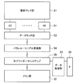
- FIG. 1 is an explanatory diagram for describing an example of a schematic circuit configuration of a solid-state imaging device according to the present embodiment.
- the solid-state imaging device 10 according to the present embodiment will be described as one in which the first substrate 20 and the second substrate 30 are stacked.
- each pixel 40 of the pixel array unit 21 is based on an address signal given from the second substrate 30 side.
- a row selection unit 25 is provided which selects in units of rows.
- the configuration in which the row selection unit 25 is provided on the first substrate 20 side has been described, the configuration may be provided on the second substrate 30 side.
- the unit pixel 40 has, for example, a photodiode 41 as a photoelectric conversion element.
- the unit pixel 40 has four transistors, for example, a transfer transistor (transfer gate) 42, a reset transistor 43, an amplification transistor 44, and a selection transistor 45, in addition to the photodiode 41.
- N-channel transistors are used as the four transistors 42 to 45.
- the combination of the conductivity types of the transfer transistor 42, the reset transistor 43, the amplification transistor 44, and the selection transistor 45 illustrated here is merely an example, and the combination is not limited to these combinations. That is, as necessary, a combination using p-channel transistors can be employed.
- the transfer signal TRG which is a drive signal for driving the pixel 40, the reset signal RST, and the selection signal SEL are appropriately supplied from the row selection unit 25 to the unit pixel 40. That is, the transfer signal TRG is applied to the gate electrode of the transfer transistor 42, the reset signal RST is applied to the gate electrode of the reset transistor 43, and the selection signal SEL is applied to the gate electrode of the selection transistor 45.
- the anode electrode of the photodiode 41 is connected to the low potential side power supply (for example, the ground), and the received light (incident light) is photoelectrically converted into photocharge (here, photoelectrons) having a charge amount according to the light amount. And accumulate the light charge.
- the cathode electrode of the photodiode 41 is electrically connected to the gate electrode of the amplification transistor 44 via the transfer transistor 42.
- a node 46 electrically connected to the gate electrode of the amplification transistor 44 is called an FD (floating diffusion / floating diffusion region) portion.
- the transfer transistor 42 is connected between the cathode electrode of the photodiode 41 and the FD unit 46.
- a transfer signal TRG of high level for example, VDD level
- high active is applied from the row selection unit 25 to the gate electrode of the transfer transistor 42.
- the transfer transistor 42 becomes conductive, and transfers the photocharge photoelectrically converted by the photodiode 41 to the FD unit 46.
- the drain electrode of the reset transistor 43 is connected to the pixel power supply VDD, and the source electrode is connected to the FD unit 46.
- a high active reset signal RST is supplied from the row selection unit 25 to the gate electrode of the reset transistor 43.
- the reset transistor 43 becomes conductive, and the charge of the FD unit 46 is discarded to the pixel power supply VDD, thereby resetting the FD unit 46.
- the gate electrode of the amplification transistor 44 is connected to the FD unit 46, and the drain electrode is connected to the pixel power supply VDD. Then, the amplification transistor 44 outputs the potential of the FD unit 46 after being reset by the reset transistor 43 as a reset signal (reset level) Vreset. Further, the amplification transistor 44 outputs the potential of the FD unit 46 after the signal charge is transferred by the transfer transistor 42 as a light accumulation signal (signal level) Vsig.
- the drain electrode of the selection transistor 45 is connected to the source electrode of the amplification transistor 44, and the source electrode is connected to the signal line 26.
- a high active selection signal SEL is applied from the row selection unit 25 to the gate electrode of the selection transistor 45.
- the selection transistor 45 is turned on, the unit pixel 40 is selected, and the signal output from the amplification transistor 44 is read out to the signal line 26.
- the potential of the FD unit 46 after reset is set as the reset level Vreset, and then the potential of the FD unit 46 after transfer of the signal charge is set as the signal level Vsig. 26 will be read.
- the signal level Vsig also includes the component of the reset level Vreset.
- the selection transistor 45 has a circuit configuration connected between the source electrode of the amplification transistor 44 and the signal line 26, but has a circuit configuration connected between the pixel power supply VDD and the drain electrode of the amplification transistor 44. It is also possible to take
- the unit pixel 40 is not limited to the pixel configuration including the four transistors described above.
- the pixel configuration includes three transistors in which the amplification transistor 44 has the function of the selection transistor 45, and the pixel configuration in which transistors after the FD unit 46 are shared between a plurality of photoelectric conversion elements (between pixels).
- the configuration of the pixel circuit does not matter.
- circuit configuration on the second board side Next, the circuit configuration on the second substrate 30 side will be described with reference to FIG.
- the current source 35, the decoder 36, the row decoder 37, and the interface (IF) A unit 38 and the like are provided.
- the current source 35 is connected to each of the signal lines 26 from which signals are read out from each pixel 40 of the pixel array unit 21 for each pixel column.
- the current source 35 has, for example, a so-called load MOS circuit configuration including a MOS transistor whose gate potential is biased to a constant potential so as to supply a constant current to the signal line 26.
- the current source 35 composed of the load MOS circuit operates the amplification transistor 44 as a source follower by supplying a constant current to the amplification transistor 44 of the unit pixel 40 in the selected row.
- the decoder 36 Under the control of the control unit 34, when selecting the pixels 40 of the pixel array unit 21 row by row under the control of the control unit 34, the decoder 36 provides the row selection unit 25 with an address signal specifying an address of the selected row.
- the row decoder 37 designates a row address when writing pixel data to the memory unit 32 or reading pixel data from the memory unit 32 under the control of the control unit 34.
- the signal processing unit 31 has at least an AD converter 51 that digitizes (AD converts) an analog pixel signal read out from each pixel 40 of the pixel array unit 21 through the signal line 26, and the pixel corresponding to the analog pixel signal Signal processing (column parallel AD) is performed in parallel in units of columns.
- AD converter 51 digitizes (AD converts) an analog pixel signal read out from each pixel 40 of the pixel array unit 21 through the signal line 26, and the pixel corresponding to the analog pixel signal Signal processing (column parallel AD) is performed in parallel in units of columns.
- the signal processing unit 31 further includes a reference voltage generation unit 52 that generates a reference voltage used for AD conversion in the AD converter 51.
- the reference voltage generation unit 52 generates a reference voltage of a so-called ramp (RAMP) waveform (tilted waveform) whose voltage value changes stepwise as time passes.
- RAMP ramp
- the reference voltage generation unit 52 can be configured, for example, using a DAC (digital-analog conversion) circuit.
- the AD converter 51 is provided, for example, for each pixel column of the pixel array unit 21, that is, for each signal line 26. That is, the AD converters 51 are so-called column parallel AD converters which are arranged by the number of pixel columns of the pixel array unit 21. Then, the AD converter 51 generates, for example, a pulse signal having a size (pulse width) in the time axis direction corresponding to the magnitude of the level of the pixel signal, and sets the length of the pulse width of the pulse signal to Perform AD conversion processing by measuring.
- the AD converter 51 is configured to have at least a comparator (COMP) 511 and a counter 512.
- the comparator 511 uses the analog pixel signals (the signal level Vsig and the reset level Vreset described above) read out from each pixel 40 of the pixel array unit 21 through the signal line 26 as a comparison input, and the ramp wave supplied from the reference voltage generation unit 52
- the reference voltage Vref of is used as a reference input, and both inputs are compared.
- the output of the comparator 511 becomes the first state (for example, high level) when the reference voltage Vref becomes larger than the pixel signal, and the output becomes the second state when the reference voltage Vref is lower than the pixel signal. State (eg, low level).
- the output signal of the comparator 511 is a pulse signal having a pulse width corresponding to the magnitude of the level of the pixel signal.
- the counter 512 for example, an up / down counter is used.
- the clock CK is applied to the counter 512 at the same timing as the supply start timing of the reference voltage Vref to the comparator 511.
- the counter 512 which is an up / down counter, performs down (DOWN) counting or up (UP) counting in synchronization with the clock CK, thereby to compare the pulse width of the output pulse of the comparator 511, that is, the comparison operation. Measure the comparison period from the start of the step to the end of the comparison operation.
- the counter 512 counts down on the reset level Vreset and the count up on the signal level Vsig for the reset level Vreset and the signal level Vsig sequentially read from the unit pixel 40.
- the AD converter 51 performs CDS (Correlated Double Sampling) processing in addition to the AD conversion processing.
- CDS Correlated Double Sampling
- the “CDS process” is a process of removing fixed pattern noise specific to a pixel such as reset noise of the unit pixel 40 or threshold variation of the amplification transistor 44 by taking a difference between the signal level Vsig and the reset level Vreset. It is. Then, the count result (count value) of the counter 512 becomes a digital value obtained by digitizing the analog pixel signal.
- FIG. 2 is a block diagram showing an example of the configuration of the signal processing unit 31 in the solid-state imaging device 10 according to the present embodiment.
- the signal processing unit 31 shown in FIG. 2 has a data latch unit 53 and a parallel-serial conversion unit 54 in addition to the AD converter 51, and the pixel data digitized by the AD converter 51 is piped to the memory unit 32. It has a pipeline configuration for line transfer. At that time, the signal processing unit 31 performs digitization processing by the AD converter 51 within one horizontal period, and performs processing of transferring digitized pixel data to the data latch unit 53 within the next one horizontal period.
- memory unit 32 is provided with a column decoder / sense amplifier 39 as its peripheral circuit. While the row decoder 37 (see FIG. 1) described above specifies a row address for the memory unit 32, the column decoder specifies a column address for the memory unit 32. In addition, the sense amplifier amplifies a weak voltage read from the memory unit 32 through the bit line to a level at which it can be handled as a digital level. The pixel data read out through the column decoder / sense amplifier 39 is output to the outside of the second substrate 30 through the data processing unit 33 and the interface unit 38.
- the present invention is not limited thereto. Two or more AD converters 51 are provided, and these two or more AD converters 51 are provided. It is also possible to adopt a configuration in which digitization processing is performed in parallel.
- two or more AD converters 51 are separately disposed in the extending direction of the signal line 26 of the pixel array unit 21, that is, in the upper and lower sides of the pixel array unit 21.
- two or more (two systems) data latch units 53, parallel-serial conversion units 54, memory units 32, etc. are provided correspondingly.
- a solid-state imaging device adopting a configuration in which, for example, two systems of AD converters 51 and the like are provided, row scanning is performed in units of two pixel rows. Then, the signal of each pixel in one pixel row is read out to one side in the vertical direction of the pixel array unit 21, and the signal of each pixel in the other pixel row is read out to the other side in the vertical direction of the pixel array unit 21,
- the two AD converters 51 perform digitization processing in parallel. The subsequent signal processing is also performed in parallel. As a result, high-speed readout of pixel data can be realized as compared to the case where row scanning is performed in units of one pixel row.
- FIG. 3 is a diagram showing an outline of a configuration example of a stacked solid-state imaging device to which the technology according to the present disclosure can be applied.
- the diagram shown in the upper part of FIG. 3 shows a schematic configuration example of the non-stacked type solid-state imaging device.
- the solid-state imaging device 330 shown in the upper part of FIG. 3 has one die (semiconductor substrate) 331.
- a pixel region 332 in which pixels are arranged in an array a control circuit 333 which performs various control such as driving of the pixels, and a logic circuit 334 for signal processing are mounted. .
- FIG. 3 show an example of a schematic configuration of the stacked solid-state imaging device.
- the solid-state imaging device 340 shown in the middle part of FIG. 3 two dies of a sensor die 341 and a logic die 342 are stacked and electrically connected to constitute one semiconductor chip.
- the pixel region 343 and the control circuit 344 are mounted on the sensor die 341, and the logic circuit 345 including a signal processing circuit that performs signal processing is mounted on the logic die 342.
- the sensor die 341 corresponds to an example of the “first substrate”
- the logic die 342 corresponds to an example of the “second substrate”.
- the solid-state imaging device 350 shown in the lower part of FIG. 3 two dies of the sensor die 351 and the logic die 352 are stacked and electrically connected to constitute one semiconductor chip.
- the pixel region 353 is mounted on the sensor die 351, and the control circuit 354 and the logic circuit 355 including the above-described signal processing circuit are mounted on the logic die 353.
- the sensor die 351 corresponds to an example of the “first substrate”
- the logic die 352 corresponds to an example of the “second substrate”.
- a random number may be used as a key for encryption.
- a method of generating the above-described random number for example, a method using thermal noise generated in an output from a predetermined device, a method using an indefinite circuit, and the like are generally known.
- the technology relating to the electronic signature described above is also expected to be applied to the protection of various information such as image data output from a solid-state imaging device, for example.
- the use of random numbers with higher randomness in the generation of a code to be used for electronic signature works more effectively by improving the security.
- the present disclosure proposes a technique capable of generating a seed value of random numbers in a more preferable manner by using the characteristics of a solid-state imaging device.
- FIG. 4 is a block diagram showing an example of a schematic functional configuration of a system to which the solid-state imaging device according to the present embodiment is applied.
- the system 1 includes a pixel array unit 21, an information processing unit 100, and a terminal device 200.
- the pixel array unit 21 and the information processing unit 100 correspond to the solid-state imaging device 10 according to the present embodiment.
- the pixel array unit 21 corresponds to the pixel array unit 21 shown in FIG.
- the information processing unit 100 corresponds to at least a part of the data processing unit 33 shown in FIG.
- a part such as a configuration related to signal processing of pixel signals Illustration of the configuration of is omitted. That is, in the present description, it is assumed that the pixel array unit 21 shown in FIG. 4 outputs pixel data after performing various signal processing on pixel signals output from each pixel.
- the information processing unit 100 includes a crop processing unit 110, a seed generation unit 120, a random number generation unit 130, a hash calculation unit 140, and a signature generation unit 150. Further, in a predetermined storage area of the information processing unit 100, a secret key D111 and a parameter D131 used for generating an electronic signature and a certificate D115 corresponding to the secret key D111 are held readably.
- the crop processing unit 110 cuts out pixel data of a region to be displayed among pixel data of each pixel output from the pixel array unit 21, and outputs the pixel data as image data to the outside (for example, the terminal device 200).
- the seed generation unit 120 obtains pixel data of the target pixel from the pixel array unit 21 with at least a part of pixels (predetermined one or more pixels) among the plurality of pixels included in the pixel array unit 21 as the target pixel. Do. Note that all pixels included in the pixel array unit 21 may be set as target pixels, or only some pixels may be set as target pixels. Also, the pixels in the optical black area or the invalid area may be included in the target pixel.
- the seed generation unit 120 generates a seed value having a bit length larger than the number of bits corresponding to the bit depth of the pixel value based on the acquired pixel value indicated by the acquired pixel data corresponding to the target pixel. .
- the seed value is used to generate a random number.
- the bit length of the seed value is not particularly limited as long as the condition regarding the relationship between the bit depth of the pixel value and the bit length of the generated seed value is satisfied.
- the bit length of the seed value is, for example, any of 32, 64, 128, 256, and 512 bits. May be The operation of the seed generation unit 120 (in particular, processing related to generation of a seed value) will be described later in detail. Then, the seed generation unit 120 outputs information indicating the generated seed value to the random number generation unit 130.
- the random number generation unit 130 corresponds to a so-called random number generator.
- the random number generation unit 130 acquires information indicating a seed value from the seed generation unit 120, and generates a random number having a predetermined bit length based on the seed value. If a random number is generated based on the acquired seed value (that is, the seed value based on the pixel value of the target pixel), the method and configuration relating to the generation of the random number are not particularly limited. Then, the random number generation unit 130 outputs information indicating the generated random number to the signature generation unit 150.
- the hash calculation unit 140 calculates a hash value based on pixel data of at least a part of pixels output to the outside as image data among pixel data of each pixel output from the pixel array unit 21.
- the hash value is used for generation of the electronic signature by the signature generation unit 150 described later. Further, the hash value may be used by another device (for example, the terminal device 200) to verify the legitimacy of the data of the electronic signature generated by the signature generation unit 150 described later.
- the hash operation unit 140 outputs information indicating the calculated hash value to the signature generation unit 150.
- the signature generation unit 150 acquires information indicating the random number generated from the random number generation unit 130. In addition, the signature generation unit 150 acquires, from the hash operation unit 140, information indicating the hash value calculated by the hash operation unit 140. The signature generation unit 150 generates an electronic signature based on the acquired random number and hash value, and the secret key D111 and parameter D131 held in a predetermined storage area. In the present description, it is assumed that an algorithm called an elliptic curve DSA (Elliptic Curve Digital Signature Algorithm) is used to generate the electronic signature. However, the generation algorithm is not necessarily limited to the elliptic curve DSA as long as the electronic signature can be generated based on the random number according to the seed value according to the present embodiment. In addition, when another generation algorithm is used, the information necessary for generating the electronic signature may be appropriately changed according to the generation algorithm.
- an algorithm Elliptic Curve Digital Signature Algorithm
- the secret key D111 corresponds to one of key pairs generated based on a so-called public key encryption technique.
- the certificate D115 is data for verifying the legitimacy of the public key (public key D113 shown in FIG. 4) to be paired with the private key D111.
- the certificate D115 includes, for example, the public key D113 and information for certifying the owner. Further, the legitimacy of the certificate D115 is verified based on the CA public key D123.
- FIG. 5 is an explanatory diagram for describing an outline of processing relating to generation of key information based on the technique of public key encryption.
- the generation of the secret key D111 and the public key D113 is performed, for example, through a procedure with a certificate authority (CA). Specifically, generation of the key pair generates the secret key D111 and the public key D113 (that is, the secret key D111 and the public key D113 shown in FIG. 4). Also, the generated public key D113 is distributed to other devices by a predetermined method. Further, as described above, the certificate D115 includes the public key D113 and information certifying its owner, and is used to confirm the legitimacy of the public key D113. Note that the certificate D115 is given a signature based on a secret key (hereinafter also referred to as "CA secret key D121”) generated by the certificate authority in order to prevent falsification.
- CA secret key D121 a secret key generated by the certificate authority in order to prevent falsification.
- the other device is a public key that pairs the validity of the signature of the certificate D115 (that is, the signature by the certificate authority) with the CA private key D121 generated by the certificate authority (hereinafter referred to as “CA public key D123 (Also referred to as “)”.
- CA public key D123 is distributed to other devices by a certificate generated by the certificate authority (hereinafter, also referred to as "CA certificate D125").
- the CA public key D123 shown in FIG. 5 corresponds to the CA public key D123 shown in FIG.
- a parameter D131 shown in FIG. 4 schematically shows various parameters used to generate the electronic signature.
- the elliptic curve DSA is used for the generation algorithm of the electronic signature
- the elliptic curve "CURVE" for private use
- the base point "G” the base point "G"
- the order "n” of G correspond to an example of the parameter D131.
- the generation algorithm of the electronic signature is not necessarily limited to the elliptic curve DSA. That is, the parameter D131 may be appropriately set according to the algorithm to be used.
- the signature generation unit 150 transmits the generated electronic signature to another device (for example, the terminal device 200). Also, at this time, the signature generation unit 150 associates the generated electronic signature with various information to be output (for example, image data etc.), and outputs the information associated with the electronic signature to another device. You may
- the terminal device 200 corresponds to, for example, a device that uses image data based on the imaging result of the solid-state imaging device 10.
- the terminal device 200 uses image data based on an imaging result by the solid-state imaging device 10 as display information (for example, an image such as a still image or a moving image) like a smartphone or the like. Display on a predetermined output unit.
- the terminal device 200 includes an image processing unit 210, hash calculation units 220 and 240, a signature verification unit 230, a certificate verification unit 250, and a display control unit 260. Also, in a predetermined storage area of the terminal device 200, the public key D113 and parameter D133 used for electronic signature verification, and the CA public key D123 and parameter D135 used for verification of the certificate D115 are held readable. It is done.
- the image processing unit 210 performs predetermined image processing on the image data output from the information processing unit 100, and outputs the image data after the image processing to the display control unit 260.
- the hash operation unit 240 and the certificate verification unit 250 are configured to verify the legitimacy of the public key D 113 which is the pair of the secret key D 111 described above.
- the hash operation unit 240 acquires the certificate D115 from the information processing unit 100, and calculates a hash value based on the data of the certificate D115. The hash value is used to verify the validity of the certificate D115. Then, the hash operation unit 240 outputs information indicating the calculated hash value to the certificate verification unit 250.
- the certificate verification unit 250 acquires the hash value calculated based on the data of the certificate D115 from the hash calculation unit 240, and verifies the validity of the data of the certificate D115 based on the hash value.
- the other hash value for verifying the legitimacy of the data of the certificate D 115 which is the comparison target of the hash values acquired from the hash operation unit 240, is acquired in advance as part of, for example, the parameter D135. May be
- the certificate verification unit 250 verifies the validity of the certificate D115 by confirming the signature given to the certificate D115 based on the CA public key D123 acquired in advance.
- the certificate verification unit 250 verifies the validity of the public key D113 based on the certificate D115.
- the terminal device 200 may acquire the correct public key D113. If possible, the method is not particularly limited.
- the certificate D115 may be used to distribute the public key D113. In this case, the certificate D115 including the data of the public key D113 is distributed to the terminal device 200.
- the terminal device 200 verifies the validity of the certificate D115 acquired based on the CA public key D123, and acquires the public key D113 included in the certificate D115 when the validity of the certificate D115 is confirmed. Just do it. That is, the validity of the public key D113 thus acquired is guaranteed by the certificate D115.
- the method of distributing the certificate D115 including the data of the public key D113 is not particularly limited.
- the terminal device 200 may hold the certificate D115.
- the certificate D115 may be published at a predetermined public site.
- the certificate verification unit 250 may notify the display control unit 260 of the verification result of the validity of the certificate D115.
- the hash calculation unit 220 calculates a hash value based on pixel data of at least a part of pixels of the image data output from the information processing unit 100.
- the hash value is used to verify the legitimacy of the data of the electronic signature that is mainly output from the information processing unit 100 (the signature generation unit 150). That is, it is desirable that the method of calculating the hash value by the hash operation unit 220 is substantially the same as that of the hash operation unit 140 described above.
- the hash operation unit 220 outputs information indicating the calculated hash value to the signature verification unit 230.
- the signature verification unit 230 acquires the electronic signature from the information processing unit 100. In addition, the signature verification unit 230 acquires, from the hash operation unit 220, information indicating the hash value calculated by the hash operation unit 220. The signature verification unit 230 verifies the validity of the electronic signature based on the acquired hash value and the public key D113 and the parameter D133 held in a predetermined storage area.
- the parameter D133 schematically indicates a parameter used for verifying the legitimacy of the electronic signature, and corresponds to, for example, the parameter D131 described above. That is, when the elliptic curve DSA is used to generate the electronic signature, the parameter D133 corresponds to a parameter for verifying the electronic signature based on the elliptic curve DSA.
- the signature verification unit 230 verifies the electronic signature to output data associated with the electronic signature, that is, data output from the information processing unit 100 such as image data. It is possible to check the original. As a result, the signature verification unit 230 can determine a device (for example, a solid-state imaging device) that is an output source of image data and the like. The signature verification unit 230 can also verify whether image data or the like has been tampered with. Then, the signature verification unit 230 notifies the display control unit 260 of the verification result of the electronic signature.
- a device for example, a solid-state imaging device
- the display control unit 260 acquires image data after image processing from the image processing unit 210, and displays information based on the image data as a predetermined output unit (for example, it corresponds to a display or the like, and is not shown in FIG. 4) Output to At this time, the display control unit 260 may control the output of the display information based on the verification result of the electronic signature notified from the signature verification unit 230. Further, the display control unit 260 may control the output of the display information based on the verification result of the certificate D 115 notified from the certificate verification unit 250.
- a predetermined output unit for example, it corresponds to a display or the like, and is not shown in FIG.
- the display control unit 260 recognizes the output source of the image data based on the notification from the signature verification unit 230, and controls the output of the display information based on the image data according to the recognition result of the output source. You may By this.
- the display control unit 260 can also execute predetermined processing (for example, an application) on only an image captured by the predetermined solid-state imaging device 10.
- the functional configuration of the system 1 described above is merely an example, and the functional configuration of the system 1 is not necessarily limited to the example illustrated in FIG. 4 as long as the operation of each configuration described above is realized.
- the information processing unit 100 and the terminal device 200 may be provided in the same case.
- the solid-state imaging device 10 according to the present embodiment that is, the pixel array unit 21 and the information processing unit 100 illustrated in FIG. 4 according to an imaging unit such as a digital camera provided in the terminal device 200 May be provided.
- at least a part of the components of the information processing unit 100 may be provided outside the information processing unit 100 (thus, the solid-state imaging device 10).
- a device provided with a configuration corresponding to the seed generation unit 120 corresponds to an example of the “information processing device”.
- a configuration for acquiring an image signal (that is, pixel data of a target pixel) used to generate a seed value from the solid-state imaging device 10 corresponds to an example of an “acquisition unit”.
- the information processing unit 100 is disposed on a die located below the die on which the pixel array unit 21 is disposed. Good.
- the information processing unit 100 may be disposed in the logic circuit 345 in the middle stage of FIG. 3 or the logic circuit 355 in the lower stage of FIG. 3.
- the information processing unit 100 (in particular, the seed generation unit 120) corresponds to an example of the “processing unit”.
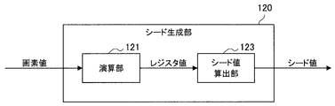
- FIG. 6 is an explanatory diagram for describing an example of a configuration related to generation of a seed value, and illustrates an example of a functional configuration of the seed generation unit 120 illustrated in FIG.
- the seed generation unit 120 includes an operation unit 121 and a seed value calculation unit 123.
- the operation unit 121 obtains pixel data corresponding to each of the target pixels, with at least a part of the plurality of pixels included in the pixel array unit 21 (one or more predetermined pixels) as the target pixel.
- the operation unit 121 calculates, for each target pixel, a register value corresponding to the target pixel by inputting a pixel value indicated by pixel data of the target pixel as input data into a predetermined register.
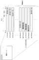
- FIG. 7 is an explanatory diagram for describing an outline of a process related to generation of a seed value.
- reference numeral D301 schematically indicates a register.
- reference symbol D303 indicates, in a bit string, input data corresponding to the pixel value of the target pixel input to the register D301.
- the register D301 has a bit length equal to the number of bits larger than the number of bits corresponding to the bit depth of the pixel value of the target pixel (that is, the number of bits corresponding to the bit length of input data).
- bit depth of the pixel value is 10 bits and the bit length of the register D301 is 32 bits is shown.
- the number of bits corresponding to the bit depth of the pixel value corresponds to an example of the “first number of bits”, and the number of bits corresponding to the bit length of the register D301 corresponds to an example of the “second number of bits”.
- the calculation unit 121 inputs the pixel value of the target pixel as the input data D303 to the register D301.
- the calculation unit 121 may shift the input data D303 input to the register D301 by the number of bits according to the pixel position of the target pixel corresponding to the input data D303 in the register D301.
- the calculation unit 121 calculates the register value for each of one or more target pixels.
- the bits of portions other than the input data D303 indicate the predetermined bit value (for example, 0) set as the initial value.
- the number of bits for shifting the input data D303 that is, the number of bits according to the pixel position corresponds to an example of the "third number of bits".
- operation unit 121 when at least a part of bits of input data D303 after the shift is included in a predetermined range in register D301, operation unit 121 reverses the order (arrangement) of each bit of input data D303. (Ie, the endianness of the bit string may be reversed). For example, in the example shown in FIG. 7, when at least a part of the bits of the input data D 303 after the shift is included in a predetermined range on the MSB (most significant bit) side in the register D 301, The order of each bit of the input data D303 is reversed.
- the calculation unit 121 may shift the input data D303 cyclically in the register D301. That is, when the position of at least a part of bits in the input data D303 exceeds the MSB of the register D301 as a result of the shift, the operation unit 121 sets the input data D303 again with the LSB of the register D301 as a base point. You may shift.
- the calculation unit 121 calculates a register value based on the pixel value of the target pixel, and outputs the register value calculated for each target pixel to the seed value calculation unit 123. .
- the seed value calculation unit 123 acquires the register value calculated for each of the one or more target pixels from the calculation unit 121, and calculates the seed value based on the acquired register value for each target pixel. As a specific example, the seed value calculation unit 123 may calculate the seed value by cumulatively adding the register value for each target pixel. The method of calculating the seed value is not particularly limited as long as the seed value is calculated based on the register value for each target pixel. Then, the seed value calculation unit 123 outputs the calculated seed value to a predetermined output destination (for example, the random number generation unit 130 shown in FIG. 4).
- a predetermined output destination for example, the random number generation unit 130 shown in FIG. 4
- the seed generation unit 120 inputs the input data D303 corresponding to the pixel value of each target pixel into the register D301, and shifts the input data D303 in the register D301 according to the pixel position of the target pixel.
- the register value is calculated by doing this.
- the seed generation unit 120 calculates a seed value based on the register value calculated for each target pixel.
- the pixel value of each pixel tends to have a larger change in the bit on the MSB side than in the bit on the LSB side.
- the influence of noise tends to be concentrated on the LSB side rather than the MSB side.
- the bit of the seed value is inverted by reversing the order of each bit of the input data D303. It is possible to further improve the uniformity of data variation in the long range.
- the seed generation unit 120 it is possible to generate random numbers of higher quality (that is, random numbers having higher randomness). That is, by generating the electronic signature based on the random number, the robustness of the electronic signature can be further improved.
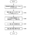
- FIG. 8 is a flowchart illustrating an example of the flow of a series of processes of the solid-state imaging device according to the present embodiment, and illustrates an example of the flow of processes relating to generation of an electronic signature.
- the information processing unit 100 sets at least a part of pixels (predetermined one or more pixels) among the plurality of pixels included in the pixel array as the target pixel, Get pixel data of The information processing unit 100 inputs, for each target pixel, a pixel value corresponding to the pixel data of the target pixel as input data into a predetermined register (S101).
- the information processing unit 100 shifts the input data input to the register by the number of bits corresponding to the pixel position of the target pixel corresponding to the input data in the register (S103).
- the information processing unit 100 calculates a register value for each target pixel, and generates a seed value by cumulatively adding the register value for each target pixel (S105).
- the information processing unit 100 (random number generation unit 130) generates a random number based on the generated seed value (S107). Further, the information processing unit 100 (the signature generation unit 150) generates an electronic signature based on the generated random number (S109). It should be noted that the electronic signature generated as described above is, for example, whether the device as the output source of the data output from the information processing unit 100 (in other words, the solid-state imaging device 10) has been identified or the data has been tampered with It is used for the verification etc.
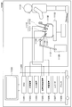
- FIG. 9 is a diagram showing an example of a schematic configuration of an endoscopic surgery system to which the technology (the present technology) according to the present disclosure can be applied.
- FIG. 9 illustrates how a surgeon (doctor) 11131 is performing surgery on a patient 11132 on a patient bed 11133 using the endoscopic surgery system 11000.
- the endoscopic operation system 11000 includes an endoscope 11100, such as pneumoperitoneum tube 11111 and the energy treatment instrument 11112, and other surgical instrument 11110, a support arm device 11120 which supports the endoscope 11100 , the cart 11200 which various devices for endoscopic surgery is mounted, and a.
- the endoscope 11100 includes a lens barrel 11101 whose region of a predetermined length from the tip is inserted into a body cavity of a patient 11132, and a camera head 11102 connected to a proximal end of the lens barrel 11101.
- the endoscope 11100 configured as a so-called rigid endoscope having a barrel 11101 of the rigid endoscope 11100, be configured as a so-called flexible scope with a barrel of flexible Good.
- the endoscope 11100 may be a straight endoscope, or may be a oblique endoscope or a side endoscope.
- An optical system and an imaging device are provided inside the camera head 11102, and the reflected light (observation light) from the observation target is condensed on the imaging device by the optical system.
- the observation light is photoelectrically converted by the imaging element to generate an electric signal corresponding to the observation light, that is, an image signal corresponding to the observation image.
- the image signal as the RAW data camera control unit: sent to (CCU Camera Control Unit) 11201.
- CCU11201 is constituted by a CPU (Central Processing Unit) or a GPU (Graphics Processing Unit) or the like, and performs overall control of the operation of the endoscope 11100 and a display device 11202. Furthermore, the CCU 11201 receives an image signal from the camera head 11102 and performs various image processing for displaying an image based on the image signal, such as development processing (demosaicing processing), on the image signal.
- image processing for displaying an image based on the image signal, such as development processing (demosaicing processing), on the image signal.
- Display device 11202 under the control of the CCU11201, displays an image based on the image signal subjected to image processing by the CCU11201.
- the light source device 11203 includes, for example, a light source such as a light emitting diode (LED), and supplies the endoscope 11100 with irradiation light at the time of imaging a surgical site or the like.
- a light source such as a light emitting diode (LED)
- LED light emitting diode
- the input device 11204 is an input interface to the endoscopic surgery system 11000.
- the user can input various information and input instructions to the endoscopic surgery system 11000 via the input device 11204.
- the user type of illumination light, magnification and focal length
- endoscopes 11100 by the imaging condition inputting the setting of the instruction or the like to change.
- Surgical instrument control unit 11205 is, tissue ablation, to control the driving of the energy treatment instrument 11112 for such sealing of the incision or blood vessel.
- the insufflation apparatus 11206 is a gas within the body cavity via the insufflation tube 11111 in order to expand the body cavity of the patient 11132 for the purpose of securing a visual field by the endoscope 11100 and securing a working space of the operator.
- Send The recorder 11207 is a device capable of recording various types of information regarding surgery.
- the printer 11208 is an apparatus capable of printing various types of information regarding surgery in various types such as text, images, and graphs.
- the light source device 11203 that supplies the irradiation light when imaging the surgical site to the endoscope 11100 can be configured of, for example, an LED, a laser light source, or a white light source configured by a combination of these. If a white light source by a combination of RGB laser light source is constructed, since it is possible to control the output intensity and output timing of each color (each wavelength) with high accuracy, the adjustment of the white balance of the captured image in the light source apparatus 11203 It can be carried out.
- a color image can be obtained without providing a color filter in the imaging device.
- the drive of the light source device 11203 may be controlled so as to change the intensity of the light to be output every predetermined time. Acquiring an image at the time of controlling the driving of the image pickup device of the camera head 11102 divided in synchronization with the timing of the change of the intensity of the light, by synthesizing the image, a high dynamic no so-called underexposure and overexposure An image of the range can be generated.
- the light source device 11203 may be configured to be able to supply light of a predetermined wavelength band corresponding to special light observation.
- the special light observation for example, by utilizing the wavelength dependency of the absorption of light in body tissue, the irradiation light in normal observation (i.e., white light) by irradiation with light of a narrow band as compared to the mucosal surface
- the so-called narrow band imaging is performed to image a predetermined tissue such as a blood vessel with high contrast.
- fluorescence observation may be performed in which an image is obtained by fluorescence generated by irradiation with excitation light.
- body tissue is irradiated with excitation light and fluorescence from the body tissue is observed (autofluorescence observation), or a reagent such as indocyanine green (ICG) is locally injected into body tissue and the body tissue is Excitation light corresponding to the fluorescence wavelength of the reagent can be irradiated to obtain a fluorescence image or the like.
- Light source device 11203 such may be configured to provide a narrow-band light and / or the excitation light corresponding to the special light observation.
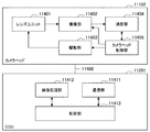
- FIG. 10 is a block diagram showing an example of functional configurations of the camera head 11102 and the CCU 11201 shown in FIG.
- the camera head 11102 includes a lens unit 11401, an imaging unit 11402, a drive unit 11403, a communication unit 11404, and a camera head control unit 11405.
- the CCU 11201 includes a communication unit 11411, an image processing unit 11412, and a control unit 11413. Camera head 11102 and CCU11201 are communicatively connected to each other by a transmission cable 11400.
- Lens unit 11401 is an optical system provided in the connecting portion of the barrel 11101. Observation light taken from the tip of the barrel 11101 is guided to the camera head 11102, incident on the lens unit 11401.
- the lens unit 11401 is configured by combining a plurality of lenses including a zoom lens and a focus lens.
- the imaging unit 11402 includes an imaging element.
- the imaging device constituting the imaging unit 11402 may be one (a so-called single-plate type) or a plurality (a so-called multi-plate type).
- an image signal corresponding to each of RGB may be generated by each imaging element, and a color image may be obtained by combining them.
- the imaging unit 11402 is, 3D (Dimensional) may be configured to have a pair of image pickup elements for obtaining respective image signals for the right eye and the left eye corresponding to the display. By 3D display is performed, the operator 11131 is enabled to grasp the depth of the living tissue in the operative site more accurately.
- the imaging unit 11402 is to be composed by multi-plate, corresponding to the imaging elements, the lens unit 11401 may be provided a plurality of systems.
- the imaging unit 11402 may not necessarily provided in the camera head 11102.
- the imaging unit 11402 may be provided inside the lens barrel 11101 immediately after the objective lens.
- the driving unit 11403 is configured by an actuator, and moves the zoom lens and the focusing lens of the lens unit 11401 by a predetermined distance along the optical axis under the control of the camera head control unit 11405. Thereby, the magnification and the focus of the captured image by the imaging unit 11402 can be appropriately adjusted.
- the communication unit 11404 is configured of a communication device for transmitting and receiving various types of information to and from the CCU 11201.
- the communication unit 11404 transmits the image signal obtained from the imaging unit 11402 to CCU11201 via a transmission cable 11400 as RAW data.
- the communication unit 11404 also receives a control signal for controlling the drive of the camera head 11102 from the CCU 11201 and supplies the control signal to the camera head control unit 11405.
- the the control signal for example, information that specifies the frame rate of the captured image, information that specifies the exposure value at the time of imaging, and / or magnification and information, etc. indicating that specifies the focal point of the captured image, captured Contains information about the condition.
- the imaging conditions such as the frame rate, exposure value, magnification, and focus described above may be appropriately designated by the user, or may be automatically set by the control unit 11413 of the CCU 11201 based on the acquired image signal. Good. In the latter case, the so-called AE (Auto Exposure) function, AF (Auto Focus) function, and AWB (Auto White Balance) function are incorporated in the endoscope 11100.
- AE Auto Exposure
- AF Auto Focus
- AWB Automatic White Balance
- the camera head control unit 11405 controls the drive of the camera head 11102 based on the control signal from the CCU 11201 received via the communication unit 11404.
- the communication unit 11411 is configured by a communication device for transmitting and receiving various types of information to and from the camera head 11102.
- the communication unit 11411 is, from the camera head 11102 receives image signals transmitted via a transmission cable 11400.
- the communication unit 11411 transmits a control signal for controlling driving of the camera head 11102 to the camera head 11102.
- the image signal and the control signal can be transmitted by telecommunication or optical communication.
- An image processing unit 11412 performs various types of image processing on an image signal that is RAW data transmitted from the camera head 11102.
- Control unit 11413 the imaging of the operated portion due endoscope 11100, and various types of control related to the display of the captured image obtained by the imaging of the surgical section are performed.
- the control unit 11413 generates a control signal for controlling the driving of the camera head 11102.
- control unit 11413 causes the display device 11202 to display a captured image in which a surgical site or the like is captured, based on the image signal subjected to the image processing by the image processing unit 11412.
- the control unit 11413 may recognize various objects in the captured image using various image recognition techniques. For example, the control unit 11413, by detecting the edge of the shape and color of an object or the like included in the captured image, the surgical instrument such as forceps, a specific body part, bleeding, during use of the energy treatment instrument 11112 mist etc. It can be recognized.
- the control unit 11413 may superimpose various surgical support information on the image of the surgery section using the recognition result. The operation support information is superimposed and presented to the operator 11131, whereby the burden on the operator 11131 can be reduced and the operator 11131 can reliably proceed with the operation.
- a transmission cable 11400 connecting the camera head 11102 and the CCU 11201 is an electric signal cable corresponding to communication of an electric signal, an optical fiber corresponding to optical communication, or a composite cable of these.
- the technology according to the present disclosure may be applied to the imaging unit 11402 of the camera head 11102 among the configurations described above.
- the solid-state imaging device 10 described with reference to FIGS. 1 to 3 is applied to the imaging unit 11402 of the camera head 11102 so that the output source of the image imaged by the imaging unit 11402 is the imaging unit.
- An electronic signature certifying that it is 11402 can be generated inside the imaging unit 11402. That is, based on the electronic signature, another apparatus using the image can verify whether the output source of the image is the imaging unit 11402 or not.
- an application target of processing (application) executed by the other apparatus is limited to only an image captured by the imaging unit 11402.
- FIG. 11 is a block diagram showing a schematic configuration example of a vehicle control system which is an example of a mobile object control system to which the technology according to the present disclosure can be applied.
- Vehicle control system 12000 includes a plurality of electronic control units connected via communication network 12001.
- the vehicle control system 12000 includes a drive system control unit 12010, a body system control unit 12020, an external information detection unit 12030, an in-vehicle information detection unit 12040, and an integrated control unit 12050.
- a microcomputer 12051, an audio image output unit 12052, and an in-vehicle network I / F (interface) 12053 are illustrated as a functional configuration of the integrated control unit 12050.
- the driveline control unit 12010 controls the operation of devices related to the driveline of the vehicle according to various programs.
- the drive system control unit 12010 includes a drive force generation device for generating a drive force of a vehicle such as an internal combustion engine or a drive motor, a drive force transmission mechanism for transmitting the drive force to the wheels, and a steering angle of the vehicle. adjusting steering mechanism, and functions as a control device of the braking device or the like to generate a braking force of the vehicle.
- Body system control unit 12020 controls the operation of the camera settings device to the vehicle body in accordance with various programs.
- the body system control unit 12020 functions as a keyless entry system, a smart key system, a power window device, or a control device of various lamps such as a headlamp, a back lamp, a brake lamp, a blinker or a fog lamp.
- the body system control unit 12020 the signal of the radio wave or various switches is transmitted from wireless controller to replace the key can be entered.
- Body system control unit 12020 receives an input of these radio or signal, the door lock device for a vehicle, the power window device, controls the lamp.
- Outside vehicle information detection unit 12030 detects information outside the vehicle equipped with vehicle control system 12000.
- an imaging unit 12031 is connected to the external information detection unit 12030.
- the out-of-vehicle information detection unit 12030 causes the imaging unit 12031 to capture an image outside the vehicle, and receives the captured image.
- the external information detection unit 12030 may perform object detection processing or distance detection processing of a person, a vehicle, an obstacle, a sign, characters on a road surface, or the like based on the received image.
- Imaging unit 12031 receives light, an optical sensor for outputting an electric signal corresponding to the received light amount of the light.
- the imaging unit 12031 can output an electric signal as an image or can output it as distance measurement information.
- the light image pickup unit 12031 is received may be a visible light, it may be invisible light such as infrared rays.
- Vehicle information detection unit 12040 detects the vehicle information.
- a driver state detection unit 12041 that detects a state of a driver is connected to the in-vehicle information detection unit 12040.
- the driver state detection unit 12041 includes, for example, a camera for imaging the driver, and the in-vehicle information detection unit 12040 determines the degree of fatigue or concentration of the driver based on the detection information input from the driver state detection unit 12041. It may be calculated or it may be determined whether the driver does not go to sleep.
- the microcomputer 12051 calculates a control target value of the driving force generation device, the steering mechanism or the braking device based on the information inside and outside the vehicle acquired by the outside information detecting unit 12030 or the in-vehicle information detecting unit 12040, and a drive system control unit A control command can be output to 12010.
- the microcomputer 12051 is collision avoidance or cushioning of the vehicle, follow-up running based on inter-vehicle distance, vehicle speed maintained running, functions realized in the vehicle collision warning, or ADAS including lane departure warning of the vehicle (Advanced Driver Assistance System) It is possible to perform coordinated control aiming at
- the microcomputer 12051 the driving force generating device on the basis of the information around the vehicle acquired by the outside information detection unit 12030 or vehicle information detection unit 12040, by controlling the steering mechanism or braking device, the driver automatic operation such that autonomously traveling without depending on the operation can be carried out cooperative control for the purpose of.
- the microcomputer 12051 can output a control command to the body system control unit 12020 based on the information outside the vehicle acquired by the external information detection unit 12030.
- the microcomputer 12051 controls the headlamps in response to the preceding vehicle or the position where the oncoming vehicle is detected outside the vehicle information detection unit 12030, the cooperative control for the purpose of achieving the anti-glare such as switching the high beam to the low beam It can be carried out.
- Audio and image output unit 12052 transmits, to the passenger or outside of the vehicle, at least one of the output signal of the voice and image to be output device to inform a visually or aurally information.
- an audio speaker 12061, a display unit 12062, and an instrument panel 12063 are illustrated as output devices.
- Display unit 12062 may include at least one of the on-board display and head-up display.
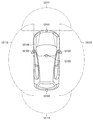
- FIG. 12 is a diagram illustrating an example of the installation position of the imaging unit 12031.
- the vehicle 12100 includes imaging units 12101, 12102, 12103, 12104, and 12105 as the imaging unit 12031.
- the imaging units 12101, 12102, 12103, 12104, and 12105 are provided, for example, at positions such as the front nose of the vehicle 12100, a side mirror, a rear bumper, a back door, and an upper portion of a windshield of a vehicle interior.
- the imaging unit 12101 provided in the front nose and the imaging unit 12105 provided in the upper part of the windshield in the vehicle cabin mainly acquire an image in front of the vehicle 12100.
- the imaging units 12102 and 12103 included in the side mirror mainly acquire an image of the side of the vehicle 12100.
- the imaging unit 12104 provided in the rear bumper or the back door mainly acquires an image of the rear of the vehicle 12100. Images in the front acquired by the imaging units 12101 and 12105 are mainly used to detect a preceding vehicle or a pedestrian, an obstacle, a traffic light, a traffic sign, a lane, or the like.
- FIG. 12 shows an example of the imaging range of the imaging units 12101 to 12104.
- Imaging range 12111 indicates an imaging range of the imaging unit 12101 provided in the front nose
- imaging range 12112,12113 are each an imaging range of the imaging unit 12102,12103 provided on the side mirror
- an imaging range 12114 is The imaging range of the imaging part 12104 provided in the rear bumper or the back door is shown.
- a bird's eye view of the vehicle 12100 viewed from above can be obtained.
- At least one of the imaging unit 12101 through 12104 may have a function of obtaining distance information.
- at least one of the imaging units 12101 to 12104 may be a stereo camera including a plurality of imaging devices, or an imaging device having pixels for phase difference detection.
- the microcomputer 12051 based on the distance information obtained from to no imaging unit 12101 12104, and the distance to the three-dimensional object in to no imaging range 12111 in 12114, the temporal change of the distance (relative speed with respect to the vehicle 12100) In particular, it is possible to extract a three-dimensional object traveling at a predetermined speed (for example, 0 km / h or more) in substantially the same direction as the vehicle 12100 as a leading vehicle, in particular by finding the it can. Further, the microcomputer 12051 can set an inter-vehicle distance to be secured in advance before the preceding vehicle, and can perform automatic brake control (including follow-up stop control), automatic acceleration control (including follow-up start control), and the like. Automatic operation or the like for autonomously traveling without depending on the way of the driver operation can perform cooperative control for the purpose.
- automatic brake control including follow-up stop control
- automatic acceleration control including follow-up start control
- the microcomputer 12051 converts three-dimensional object data relating to three-dimensional objects into two-dimensional vehicles such as two-wheeled vehicles, ordinary vehicles, large vehicles, classification and extracted, can be used for automatic avoidance of obstacles.
- the microcomputer 12051 identifies obstacles around the vehicle 12100 into obstacles visible to the driver of the vehicle 12100 and obstacles difficult to see.
- the microcomputer 12051 determines a collision risk which indicates the risk of collision with the obstacle, when a situation that might collide with the collision risk set value or more, through an audio speaker 12061, a display portion 12062 By outputting a warning to the driver or performing forcible deceleration or avoidance steering via the drive system control unit 12010, driving support for collision avoidance can be performed.
- At least one of the imaging unit 12101 to 12104 may be an infrared camera that detects infrared rays.
- the microcomputer 12051 can recognize a pedestrian by determining whether a pedestrian is present in the images captured by the imaging units 12101 to 12104.
- Such pedestrian recognition is, for example, a procedure for extracting feature points in images captured by the imaging units 12101 to 12104 as an infrared camera, and pattern matching processing on a series of feature points indicating the outline of an object to determine whether it is a pedestrian or not
- the procedure is to determine Microcomputer 12051 is, determines that the pedestrian in the captured image of the imaging unit 12101 to 12104 is present, recognizing the pedestrian, the sound image output unit 12052 is rectangular outline for enhancement to the recognized pedestrian to superimpose, controls the display unit 12062.
- the audio image output unit 12052 is, an icon or the like indicating a pedestrian may control the display unit 12062 to display the desired position.
- the technology according to the present disclosure may be applied to the imaging unit 12101 among the configurations described above.
- the solid-state imaging device 10 described with reference to FIGS. 1 to 3 is applied to the imaging unit 12101 so that the output source of the image imaged by the imaging unit 12101 is the imaging unit 12101.
- the solid-state imaging device is a random number based on the pixel array portion in which a plurality of pixels are arranged, and the pixel value of each of one or more target pixels of the plurality of pixels.
- a processing unit that generates a seed value of The pixel array unit is disposed on a first substrate.
- the processing unit is disposed on the second substrate.
- a plurality of substrates including at least a first substrate and a second substrate are positioned such that the second substrate is located below the first substrate. Be stacked.
- random noise occurs in an image captured by a solid-state imaging device. Therefore, in the solid-state imaging device according to the present embodiment, random noise generated in the image is used to generate a seed value that can be used to generate a random number.
- the processing unit uses the pixel value of the target pixel as input data for each of the one or more target pixels, and uses bits corresponding to the second bit number larger than the first bit number corresponding to the bit depth of the pixel value.
- the register value may be calculated by inputting to a register having a length.
- the processing unit generates the seed value based on the register value calculated for each of the one or more target pixels.
- a pixel array unit in which a plurality of pixels are arranged;
- a processing unit that generates a seed value of a random number based on pixel values of predetermined one or more target pixels among the plurality of pixels; Equipped with The pixel array unit is disposed on a first substrate, The processing unit is disposed on a second substrate, A plurality of substrates including at least the first substrate and the second substrate are stacked such that the second substrate is located below the first substrate.
- the processing unit is A register having a bit length corresponding to a second number of bits larger than a first number of bits corresponding to a bit depth of the pixel value, using the pixel value of the target pixel as input data for each of the one or more target pixels Calculate the register value by Generating the seed value based on the register value calculated for each of the one or more target pixels; The solid-state imaging device according to (1).
- the processing unit shifts the input data input to the register by a third bit number corresponding to the pixel position of the target pixel corresponding to the input data in the register to calculate the register value.
- the solid-state imaging device according to (2) is A register having a bit length corresponding to a second number of bits larger than a first number of bits corresponding to a bit depth of the pixel value, using the pixel value of the target pixel as input data for each of the one or more target pixels Calculate the register value by Generating the seed value based on the register value calculated for each of the one or more target pixels; The solid-state imaging
- An acquisition unit configured to acquire an image signal corresponding to each of predetermined one or more target pixels in a pixel area in which a plurality of pixels are arranged;
- a processing unit that generates a seed value of a random number based on the pixel value of each of the one or more target pixels according to the image signal;
- An information processing apparatus comprising:
Landscapes
- Engineering & Computer Science (AREA)
- Signal Processing (AREA)
- Computer Security & Cryptography (AREA)
- Computer Networks & Wireless Communication (AREA)
- Multimedia (AREA)
- Physics & Mathematics (AREA)
- General Physics & Mathematics (AREA)
- Theoretical Computer Science (AREA)
- Transforming Light Signals Into Electric Signals (AREA)
- Solid State Image Pick-Up Elements (AREA)
Abstract
【課題】固体撮像装置の特性を利用して、より好適な態様で乱数のシード値を生成する。 【解決手段】複数の画素が配列された画素アレイ部と、前記複数の画素のうちの所定の1以上の対象画素それぞれの画素値に基づき、乱数のシード値を生成する処理部と、を備え、前記画素アレイ部は、第1の基板に配置され、前記処理部は、第2の基板に配置され、少なくとも前記第1の基板と前記第2の基板とを含む複数の基板が、前記第2の基板が前記第1の基板よりも下層に位置するように積層される、固体撮像装置。
Description
本開示は、固体撮像装置及び情報処理装置に関する。
固体撮像装置として、CMOS(Complementary Metal Oxide Semiconductor)等のMOS型イメージセンサに代表される増幅型固体撮像装置が知られている。また、CCD(Charge Coupled Device)イメージセンサに代表される電荷転送型固体撮像装置が知られている。これら固体撮像装置は、デジタルスチルカメラ、デジタルビデオカメラなどに広く用いられている。また、カメラ付き携帯電話やPDA(Personal Digital Assistant)などのモバイル機器に搭載される固体撮像装置としては、電源電圧が低く、消費電力の観点などからMOS型イメージセンサが多く用いられている。
ところで、近年では、セキュリティ強化や著作権保護の観点から、暗号を利用した電子署名の需要が増加している。電子署名に利用される暗号の生成に際し、例えば、暗号化用の鍵に乱数が利用される場合がある。例えば、特許文献1には、暗号化用の鍵に利用される乱数を生成するための技術の一例が開示されている。
上述した電子署名に関する技術は、例えば、固体撮像装置から出力される画像データ等の各種情報の保護への応用も期待されている。また、電子署名に利用する暗号の生成に際し、よりランダム性の高い乱数の利用は、セキュリティ性の向上により有効に働くことが知られている。
そこで、本開示では、固体撮像装置の特性を利用して、より好適な態様で乱数のシード値を生成することが可能な技術について提案する。
本開示によれば、複数の画素が配列された画素アレイ部と、前記複数の画素のうちの所定の1以上の対象画素それぞれの画素値に基づき、乱数のシード値を生成する処理部と、を備え、前記画素アレイ部は、第1の基板に配置され、前記処理部は、第2の基板に配置され、少なくとも前記第1の基板と前記第2の基板とを含む複数の基板が、前記第2の基板が前記第1の基板よりも下層に位置するように積層される、固体撮像装置が提供される。
また、本開示によれば、複数の画素が配列された画素領域のうち所定の1以上の対象画素それぞれに対応する画像信号を取得する取得部と、前記画像信号に応じた前記1以上の対象画素それぞれの画素値に基づき、乱数のシード値を生成する処理部と、を備える、情報処理装置が提供される。
以上説明したように本開示によれば、固体撮像装置の特性を利用して、より好適な態様で乱数のシード値を生成することが可能な技術が提供される。
なお、上記の効果は必ずしも限定的なものではなく、上記の効果とともに、または上記の効果に代えて、本明細書に示されたいずれかの効果、または本明細書から把握され得る他の効果が奏されてもよい。
以下に添付図面を参照しながら、本開示の好適な実施の形態について詳細に説明する。なお、本明細書及び図面において、実質的に同一の機能構成を有する構成要素については、同一の符号を付することにより重複説明を省略する。
なお、説明は以下の順序で行うものとする。
1.固体撮像装置の構成例
1.1.固体撮像装置の概略構成
1.2.積層型の固体撮像装置の概略構成
2.電子署名の適用に関する検討
3.技術的特徴
3.1.機能構成
3.2.シード値の生成に係る構成の詳細
3.3.処理
4.応用例
4.1.内視鏡手術システムへの応用例
4.2.移動体への応用例
5.むすび
1.固体撮像装置の構成例
1.1.固体撮像装置の概略構成
1.2.積層型の固体撮像装置の概略構成
2.電子署名の適用に関する検討
3.技術的特徴
3.1.機能構成
3.2.シード値の生成に係る構成の詳細
3.3.処理
4.応用例
4.1.内視鏡手術システムへの応用例
4.2.移動体への応用例
5.むすび
<<1.固体撮像装置の構成例>>
以下に、本開示の一実施形態に係る固体撮像装置の構成の一例について説明する。
以下に、本開示の一実施形態に係る固体撮像装置の構成の一例について説明する。
<1.1.固体撮像装置の概略構成>
まず、図1及び図2を参照して、本開示の一実施形態に係る固体撮像装置の概略的な構成の一例について説明する。例えば、図1は、本実施形態に係る固体撮像装置の概略的な回路構成の一例について説明するための説明図である。なお、本説明では、本実施形態に係る固体撮像装置10は、第1基板20と第2基板30とが積層されて構成されているものとして説明する。
まず、図1及び図2を参照して、本開示の一実施形態に係る固体撮像装置の概略的な構成の一例について説明する。例えば、図1は、本実施形態に係る固体撮像装置の概略的な回路構成の一例について説明するための説明図である。なお、本説明では、本実施形態に係る固体撮像装置10は、第1基板20と第2基板30とが積層されて構成されているものとして説明する。
(第1基板側の構成例)
まず、第1基板20側の回路構成について図1を参照して説明する。第1基板20側には、単位画素40が行列状に配置されて成る画素アレイ部21の他に、第2基板30側から与えられるアドレス信号を基に、画素アレイ部21の各画素40を行単位で選択する行選択部25が設けられている。なお、ここでは、行選択部25を第1基板20側に設ける構成について説明したが、第2基板30側に設ける構成とすることも可能である。
まず、第1基板20側の回路構成について図1を参照して説明する。第1基板20側には、単位画素40が行列状に配置されて成る画素アレイ部21の他に、第2基板30側から与えられるアドレス信号を基に、画素アレイ部21の各画素40を行単位で選択する行選択部25が設けられている。なお、ここでは、行選択部25を第1基板20側に設ける構成について説明したが、第2基板30側に設ける構成とすることも可能である。
図1に示すように、単位画素40は、光電変換素子として例えばフォトダイオード41を有している。単位画素40は、フォトダイオード41に加えて、例えば、転送トランジスタ(転送ゲート)42、リセットトランジスタ43、増幅トランジスタ44、及び、選択トランジスタ45の4つのトランジスタを有している。
ここでは、4つのトランジスタ42~45として、例えばNチャネルのトランジスタを用いている。ただし、ここで例示した転送トランジスタ42、リセットトランジスタ43、増幅トランジスタ44、及び、選択トランジスタ45の導電型の組み合わせは一例に過ぎず、これらの組み合わせに限られるものではない。すなわち、必要に応じて、Pチャネルのトランジスタを用いる組み合わせとすることができる。
上記単位画素40に対して、当該画素40を駆動する駆動信号である転送信号TRG、リセット信号RST、及び、選択信号SELが行選択部25から適宜与えられる。即ち、転送信号TRGが転送トランジスタ42のゲート電極に、リセット信号RSTがリセットトランジスタ43のゲート電極に、選択信号SELが選択トランジスタ45のゲート電極にそれぞれ印加される。
フォトダイオード41は、アノード電極が低電位側電源(例えば、グランド)に接続されており、受光した光(入射光)をその光量に応じた電荷量の光電荷(ここでは、光電子)に光電変換してその光電荷を蓄積する。フォトダイオード41のカソード電極は、転送トランジスタ42を介して増幅トランジスタ44のゲート電極と電気的に接続されている。増幅トランジスタ44のゲート電極と電気的に繋がったノード46をFD(フローティングディフュージョン/浮遊拡散領域)部と呼ぶ。
転送トランジスタ42は、フォトダイオード41のカソード電極とFD部46との間に接続されている。転送トランジスタ42のゲート電極には、高レベル(例えば、VDDレベル)がアクティブ(以下、「Highアクティブ」と記述する)の転送信号TRGが行選択部25から与えられる。この転送信号TRGに応答して、転送トランジスタ42が導通状態となり、フォトダイオード41で光電変換された光電荷をFD部46に転送する。
リセットトランジスタ43は、ドレイン電極が画素電源VDDに、ソース電極がFD部46にそれぞれ接続されている。リセットトランジスタ43のゲート電極には、Highアクティブのリセット信号RSTが行選択部25から与えられる。このリセット信号RSTに応答して、リセットトランジスタ43が導通状態となり、FD部46の電荷を画素電源VDDに捨てることによって当該FD部46をリセットする。
増幅トランジスタ44は、ゲート電極がFD部46に、ドレイン電極が画素電源VDDにそれぞれ接続されている。そして、増幅トランジスタ44は、リセットトランジスタ43によってリセットされた後のFD部46の電位をリセット信号(リセットレベル)Vresetとして出力する。増幅トランジスタ44はさらに、転送トランジスタ42によって信号電荷が転送された後のFD部46の電位を光蓄積信号(信号レベル)Vsigとして出力する。
選択トランジスタ45は、例えば、ドレイン電極が増幅トランジスタ44のソース電極に、ソース電極が信号線26にそれぞれ接続されている。選択トランジスタ45のゲート電極には、Highアクティブの選択信号SELが行選択部25から与えられる。この選択信号SELに応答して、選択トランジスタ45が導通状態となり、単位画素40を選択状態として増幅トランジスタ44から出力される信号を信号線26に読み出す。
上述したことから明らかなように、単位画素40からは、リセット後のFD部46の電位がリセットレベルVresetとして、次いで、信号電荷の転送後のFD部46の電位が信号レベルVsigとして順に信号線26に読み出されることになる。因みに、信号レベルVsigには、リセットレベルVresetの成分も含まれる。
なお、ここでは、選択トランジスタ45について、増幅トランジスタ44のソース電極と信号線26との間に接続する回路構成としたが、画素電源VDDと増幅トランジスタ44のドレイン電極との間に接続する回路構成を採ることも可能である。
また、単位画素40としては、上記の4つのトランジスタから成る画素構成のものに限られるものではない。例えば、増幅トランジスタ44に選択トランジスタ45の機能を持たせた3つのトランジスタから成る画素構成や、複数の光電変換素子間(画素間)で、FD部46以降のトランジスタを共用する画素構成などであっても良く、その画素回路の構成は問わない。
(第2基板側の回路構成)
次に、第2基板30側の回路構成について図1を参照して説明する。第2基板30側には、前述した信号処理部31、メモリ部32、データ処理部33、及び、制御部34の他に、電流源35、デコーダ36、行デコーダ37、及び、インタフェース(IF)部38などが設けられている。
次に、第2基板30側の回路構成について図1を参照して説明する。第2基板30側には、前述した信号処理部31、メモリ部32、データ処理部33、及び、制御部34の他に、電流源35、デコーダ36、行デコーダ37、及び、インタフェース(IF)部38などが設けられている。
電流源35は、画素アレイ部21の各画素40から画素列毎に信号が読み出される信号線26の各々に接続されている。電流源35は、例えば、信号線26にある一定の電流を供給するように、ゲート電位が一定電位にバイアスされたMOSトランジスタから成る、所謂、負荷MOS回路の構成となっている。この負荷MOS回路から成る電流源35は、選択行の単位画素40の増幅トランジスタ44に定電流を供給することにより、当該増幅トランジスタ44をソースフォロアとして動作させる。
デコーダ36は、制御部34による制御の下に、画素アレイ部21の各画素40を行単位で選択する際に、その選択行のアドレスを指定するアドレス信号を行選択部25に対して与える。行デコーダ37は、制御部34による制御の下に、メモリ部32に画素データを書き込んだり、メモリ部32から画素データを読み出したりする際の行アドレスを指定する。
信号処理部31は、少なくとも、画素アレイ部21の各画素40から信号線26を通して読み出されるアナログ画素信号をデジタル化(AD変換)するAD変換器51を有し、当該アナログ画素信号に対して画素列の単位で並列に信号処理(列並列AD)を行う構成となっている。
信号処理部31は更に、AD変換器51でのAD変換の際に用いる参照電圧を生成する参照電圧生成部52を有する。参照電圧生成部52は、時間が経過するにつれて電圧値が階段状に変化する、所謂、ランプ(RAMP)波形(傾斜状の波形)の参照電圧を生成する。参照電圧生成部52については、例えば、DAC(デジタル-アナログ変換)回路を用いて構成することができる。
AD変換器51は、例えば、画素アレイ部21の画素列毎に、即ち、信号線26毎に設けられている。すなわち、AD変換器51は、画素アレイ部21の画素列の数だけ配置されて成る、所謂、列並列AD変換器となっている。そして、AD変換器51は、例えば、画素信号のレベルの大きさに対応した時間軸方向に大きさ(パルス幅)を持つパルス信号を生成し、当該パルス信号のパルス幅の期間の長さを計測することによってAD変換の処理を行う。
より具体的には、図2に示すように、AD変換器51は、比較器(COMP)511及びカウンタ512を少なくとも有する構成となっている。比較器511は、画素アレイ部21の各画素40から信号線26を通して読み出されるアナログ画素信号(先述した信号レベルVsigおよびリセットレベルVreset)を比較入力とし、参照電圧生成部52から供給されるランプ波の参照電圧Vrefを基準入力とし、両入力を比較する。
そして、比較器511は、例えば、参照電圧Vrefが画素信号よりも大なるときに出力が第1の状態(例えば、高レベル)になり、参照電圧Vrefが画素信号以下のときに出力が第2の状態(例えば、低レベル)になる。この比較器511の出力信号が、画素信号のレベルの大きさに対応したパルス幅を持つパルス信号となる。
カウンタ512として、例えば、アップ/ダウンカウンタが用いられる。カウンタ512には、比較器511に対する参照電圧Vrefの供給開始タイミングと同じタイミングでクロックCKが与えられる。アップ/ダウンカウンタであるカウンタ512は、クロックCKに同期してダウン(DOWN)カウント、または、アップ(UP)カウントを行うことで、比較器511の出力パルスのパルス幅の期間、即ち、比較動作の開始から比較動作の終了までの比較期間を計測する。この計測動作の際、カウンタ512は、単位画素40から順に読み出されるリセットレベルVreset及び信号レベルVsigについて、リセットレベルVresetに対してはダウンカウントを行い、信号レベルVsigに対してはアップカウントを行う。
このダウンカウント/アップカウントの動作により、信号レベルVsigとリセットレベルVresetとの差分をとることができる。その結果、AD変換器51では、AD変換処理に加えてCDS(Correlated Double Sampling:相関二重サンプリング)処理が行われる。ここで、「CDS処理」とは、信号レベルVsigとリセットレベルVresetとの差分をとることにより、単位画素40のリセットノイズや増幅トランジスタ44の閾値ばらつき等の画素固有の固定パターンノイズを除去する処理である。そして、カウンタ512のカウント結果(カウント値)が、アナログ画素信号をデジタル化したデジタル値となる。
(信号処理部の構成の一例)
次いで、本実施形態に係る固体撮像装置10における信号処理部31の構成の一例について説明する。図2は、本実施形態に係る固体撮像装置10における信号処理部31の構成の一例を示すブロック図である。
次いで、本実施形態に係る固体撮像装置10における信号処理部31の構成の一例について説明する。図2は、本実施形態に係る固体撮像装置10における信号処理部31の構成の一例を示すブロック図である。
図2に示す信号処理部31は、AD変換器51の他に、データラッチ部53及びパラレル-シリアル変換部54を有し、AD変換器51でデジタル化された画素データをメモリ部32にパイプライン転送するパイプライン構成となっている。その際、信号処理部31は、1水平期間内にAD変換器51によるデジタル化処理を行い、デジタル化した画素データを次の1水平期間内にデータラッチ部53へ転送する処理を行う。
一方、メモリ部32には、その周辺回路として列デコーダ/センスアンプ39が設けられている。先述した行デコーダ37(図1参照)がメモリ部32に対して行アドレスを指定するのに対し、列デコーダは、メモリ部32に対して列アドレスを指定する。また、センスアンプは、メモリ部32からビット線を通して読み出される微弱な電圧を、デジタルレベルとして取り扱いが可能になるレベルにまで増幅する。そして、列デコーダ/センスアンプ39を通して読み出された画素データは、データ処理部33及びインタフェース部38を介して第2基板30の外部へ出力される。
なお、ここでは、列並列のAD変換器51が1つの場合を例に挙げたが、これに限られるものではなく、AD変換器51を2つ以上設け、これら2つ以上のAD変換器51において並列的にデジタル化処理を行う構成を採ることも可能である。
この場合、2つ以上のAD変換器51は、画素アレイ部21の信号線26の伸長方向、即ち、画素アレイ部21の上下両側に分けて配置されることになる。AD変換器51を2つ以上設ける場合は、これに対応してデータラッチ部53、パラレル-シリアル変換部54、及び、メモリ部32なども2つ(2系統)以上設けることになる。
このように、AD変換器51などを例えば2系統設ける構成を採る固体撮像装置にあっては、行走査を2つの画素行を単位として行う。そして、一方の画素行の各画素の信号については画素アレイ部21の上下方向の一方側に、他方の画素行の各画素の信号については画素アレイ部21の上下方向の他方側にそれぞれ読み出し、2つのAD変換器51で並列的にデジタル化処理を行うことになる。以降の信号処理についても並列的に行う。その結果、1つの画素行を単位として行走査を行う場合に比べて、画素データの高速読み出しを実現できる。
以上、図1及び図2を参照して、本開示の一実施形態に係る固体撮像装置の概略的な構成の一例について説明した。
<1.2.積層型の固体撮像装置の概略構成>
続いて、図3を参照して、本開示に係る技術を適用し得る積層型の固体撮像装置の構成例の概要について説明する。図3は、本開示に係る技術を適用し得る積層型の固体撮像装置の構成例の概要を示す図である。
続いて、図3を参照して、本開示に係る技術を適用し得る積層型の固体撮像装置の構成例の概要について説明する。図3は、本開示に係る技術を適用し得る積層型の固体撮像装置の構成例の概要を示す図である。
まず、図3上段に示す図は、非積層型の固体撮像装置の概略構成例を示している。具体的には、図3の上段に示す固体撮像装置330は、1枚のダイ(半導体基板)331を有する。また、当該ダイ331には、画素がアレイ状に配置された画素領域332と、画素の駆動その他の各種の制御を行う制御回路333と、信号処理するためのロジック回路334とが搭載されている。
これに対して、図3の中段及び下段に示す図は、積層型の固体撮像装置の概略構成例を示している。
例えば、図3の中段に示す固体撮像装置340は、センサダイ341とロジックダイ342との2枚のダイが積層され、電気的に接続されて、1つの半導体チップとして構成されている。センサダイ341には、画素領域343と制御回路344とが搭載され、ロジックダイ342には、信号処理を行う信号処理回路を含むロジック回路345が搭載されている。なお、この場合には、センサダイ341が「第1の基板」の一例に相当し、ロジックダイ342が「第2の基板」の一例に相当する。
また、図3の下段に示す固体撮像装置350は、センサダイ351とロジックダイ352との2枚のダイが積層され、電気的に接続されて、1つの半導体チップとして構成されている。センサダイ351には、画素領域353が搭載され、ロジックダイ353には、制御回路354と、上述した信号処理回路を含むロジック回路355とが搭載されている。なお、この場合には、センサダイ351が「第1の基板」の一例に相当し、ロジックダイ352が「第2の基板」の一例に相当する。
なお、上記では、2枚のダイが積層されて1つの半導体チップとして構成された積層型の固体撮像装置の一例について説明したが、上記構成は、本実施形態に係る固体撮像装置の構成を限定するものではない。例えば、3枚以上のダイが積層されて1つの半導体チップとして構成されてもよい。
以上、図3を参照して、本開示に係る技術を適用し得る積層型の固体撮像装置の構成例の概要について説明した。
<<2.電子署名の適用に関する検討>>
近年、セキュリティ強化や著作権保護の観点から、暗号を利用した電子署名の需要が増加している。また、このような電子署名に利用される暗号の生成に際し、例えば、暗号化用の鍵に乱数が利用される場合がある。上述した乱数を生成する手法として、例えば、所定のデバイスからの出力に生じる熱雑音を利用した手法や、不定回路を利用した手法等が一般的に知られている。
近年、セキュリティ強化や著作権保護の観点から、暗号を利用した電子署名の需要が増加している。また、このような電子署名に利用される暗号の生成に際し、例えば、暗号化用の鍵に乱数が利用される場合がある。上述した乱数を生成する手法として、例えば、所定のデバイスからの出力に生じる熱雑音を利用した手法や、不定回路を利用した手法等が一般的に知られている。
特に、近年では、上述した電子署名に関する技術は、例えば、固体撮像装置から出力される画像データ等の各種情報の保護への応用も期待されている。また、電子署名に利用する暗号の生成に際し、よりランダム性の高い乱数の利用は、セキュリティ性の向上により有効に働くことが知られている。
以上のような状況を鑑み、本開示では、固体撮像装置の特性を利用して、より好適な態様で乱数のシード値を生成することが可能な技術について提案する。
<<3.技術的特徴>>
以下に、本開示の一実施形態に係る固体撮像装置の技術的特徴について説明する
以下に、本開示の一実施形態に係る固体撮像装置の技術的特徴について説明する
<3.1.機能構成>
まず、本実施形態に係る固体撮像装置を適用したシステムの概略的な構成の一例について、特に、電子署名の生成と、当該電子署名の検証とに係る部分に着目して説明する。図4は、本実施形態に係る固体撮像装置を適用したシステムの概略的な機能構成の一例を示したブロック図である。
まず、本実施形態に係る固体撮像装置を適用したシステムの概略的な構成の一例について、特に、電子署名の生成と、当該電子署名の検証とに係る部分に着目して説明する。図4は、本実施形態に係る固体撮像装置を適用したシステムの概略的な機能構成の一例を示したブロック図である。
図4に示すように、本実施形態に係るシステム1は、画素アレイ部21と、情報処理部100と、端末装置200とを含む。なお、画素アレイ部21及び情報処理部100が、本実施形態に係る固体撮像装置10に相当する。具体的には、画素アレイ部21は、図1に示す画素アレイ部21に相当する。また、情報処理部100は、図1に示すデータ処理部33の少なくとも一部に相当する。なお、図4に示す例では、本実施形態に係るシステムの特徴をよりわかりやすくするために、固体撮像装置の各構成のうち、例えば、画素信号の信号処理に係る構成等のような一部の構成の図示を省略している。即ち、本説明においては、図4に示す画素アレイ部21からは、各画素から出力される画素信号に対して各種信号処理が施された後の画素データが出力されるものとして説明する。
(情報処理装置100)
まず、情報処理部100の構成について説明する。図4に示すように、情報処理部100は、クロップ処理部110と、シード生成部120と、乱数生成部130と、ハッシュ演算部140と、署名生成部150とを含む。また、情報処理部100の所定の記憶領域には、電子署名の生成に用いられる秘密鍵D111及びパラメータD131と、当該秘密鍵D111に対応する証明書D115と、が読み出し可能に保持されている。
まず、情報処理部100の構成について説明する。図4に示すように、情報処理部100は、クロップ処理部110と、シード生成部120と、乱数生成部130と、ハッシュ演算部140と、署名生成部150とを含む。また、情報処理部100の所定の記憶領域には、電子署名の生成に用いられる秘密鍵D111及びパラメータD131と、当該秘密鍵D111に対応する証明書D115と、が読み出し可能に保持されている。
クロップ処理部110は、画素アレイ部21から出力される画素ごとの画素データのうち、表示対象となる領域の画素データを切り出して、画像データとして外部(例えば、端末装置200)に出力する。
シード生成部120は、画素アレイ部21に含まれる複数の画素のうち少なくとも一部の画素(所定の1以上の画素)を対象画素として、当該対象画素の画素データを当該画素アレイ部21から取得する。なお、画素アレイ部21に含まれる全ての画素が対象画素として設定されていてもよいし、一部の画素のみが対象画素として設定されていてもよい。また、オプティカルブラック領域や無効領域の画素が対象画素に含まれていてもよい。
シード生成部120は、取得した上記対象画素に対応する画素データが示す画素値に基づき、当該画素値のビット深度に相当するビット数よりも大きいビット数分のビット長を有するシード値を生成する。当該シード値は、乱数の生成に利用される。なお、画素値のビット深度と、生成されるシード値のビット長と、の間の関係に関する条件を満たせば、当該シード値のビット長は特に限定されない。具体的な一例として、画素値のビット深度が8、12、及び14ビット程度の場合に、シード値のビット長としては、例えば、32、64、128、256、及び512ビットのいずれかであってもよい。シード生成部120の動作(特に、シード値の生成に係る処理)については、詳細を別途後述する。そして、シード生成部120は、生成したシード値を示す情報を乱数生成部130に出力する。
乱数生成部130は、所謂乱数発生器に相当する。乱数生成部130は、シード生成部120からシード値を示す情報を取得し、当該シード値に基づき所定のビット長を有する乱数を生成する。なお、取得されたシード値(即ち、対象画素の画素値に基づくシード値)に基づき乱数が生成されれば、当該乱数の生成に係る方法や構成は特に限定されない。そして、乱数生成部130は、生成した乱数を示す情報を署名生成部150に出力する。
ハッシュ演算部140は、画素アレイ部21から出力される画素ごとの画素データのうち、画像データとして外部に出力される少なくとも一部の画素の画素データに基づきハッシュ値を算出する。当該ハッシュ値は、後述する署名生成部150による電子署名の生成に利用される。また、当該ハッシュ値は、後述する署名生成部150により生成される電子署名のデータの正当性を、他の装置(例えば、端末装置200)が検証するために用いられてもよい。ハッシュ演算部140は、算出したハッシュ値を示す情報を署名生成部150に出力する。
署名生成部150は、乱数生成部130から生成された乱数を示す情報を取得する。また、署名生成部150は、ハッシュ演算部140により算出されたハッシュ値を示す情報を当該ハッシュ演算部140から取得する。署名生成部150は、取得した乱数及びハッシュ値と、所定の記憶領域に保持された秘密鍵D111及びパラメータD131と、に基づき電子署名を生成する。なお、本説明では、電子署名の生成に、楕円曲線DSA(Elliptic Curve Digital Signature Algorithm)と呼ばれるアルゴリズムが使用されるものとして説明する。しかしながら、本実施形態に係るシード値に応じた乱数に基づき電子署名を生成することが可能であれば、生成アルゴリズムは必ずしも楕円曲線DSAには限定されない。なお、他の生成アルゴリズムが使用される場合には、当該生成アルゴリズムに応じて、電子署名の生成に必要な情報については適宜変更されてもよい。
秘密鍵D111は、所謂公開鍵暗号の技術に基づき生成される鍵のペアのうちの一方に相当する。また、証明書D115は、当該秘密鍵D111の対になる公開鍵(図4に示す公開鍵D113)の正当性を検証するためのデータである。証明書D115には、例えば、公開鍵D113とその所有者を証明する情報等が含まれる。また、証明書D115の正当性については、CA公開鍵D123に基づき検証される。
ここで、図5を参照して、公開鍵暗号の技術の概要を説明することで、秘密鍵D111、公開鍵D113、証明書D115、及びCA公開鍵D123それぞれの生成方法とその役割について説明する。例えば、図5は、公開鍵暗号の技術に基づく鍵情報の生成に係る処理の概要について説明するための説明図である。
図5に示すように、秘密鍵D111及び公開鍵D113の生成は、例えば、認証局(CA:Certificate Authority)への手続きを介して行われる。具体的には、鍵ペアの生成により、秘密鍵D111及び公開鍵D113(即ち、図4に示す秘密鍵D111及び公開鍵D113)が生成される。また、生成された公開鍵D113は、所定の方法により、他の装置に配布される。また、証明書D115は、前述した通り、公開鍵D113とその所有者を証明する情報を含み、当該公開鍵D113の正当性を確認するために用いられる。なお、証明書D115は、改ざんを防ぐために、認証局により生成された秘密鍵(以降では、「CA秘密鍵D121」とも称する)に基づき署名が付与される。また、他の装置は、証明書D115の署名(即ち、認証局による署名)の正当性を、認証局により生成されたCA秘密鍵D121と対になる公開鍵(以降では、「CA公開鍵D123」とも称する)に基づき検証する。また、CA公開鍵D123は、認証局により生成された証明書(以降では、「CA証明書D125」とも称する)により、他の装置に配布される。なお、図5に示すCA公開鍵D123が、図4に示すCA公開鍵D123に相当する。
また、図4に示すパラメータD131は、電子署名の生成に使用される各種パラメータを模式的に示している。例えば、電子署名の生成アルゴリズムに楕円曲線DSAを利用する場合には、私用する楕円曲線「CURVE」、ベースポイント「G」、及びGの位数「n」が、パラメータD131の一例に相当する。なお、上述した通り、電子署名の生成アルゴリズムは、必ずしも楕円曲線DSAのみには限定されない。即ち、パラメータD131は、使用されるアルゴリズムに応じて適宜設定されればよい。
そして、図4に示すように、署名生成部150は、生成した電子署名を他の装置(例えば、端末装置200)に送信する。また、このとき署名生成部150は、出力対象となる各種情報(例えば、画像データ等)に対して、生成した電子署名を関連付けて、当該電子署名が関連付けられた当該情報を他の装置に出力してもよい。
(端末装置200)
次いで、端末装置200の構成について説明する。端末装置200は、例えば、固体撮像装置10の撮像結果に基づく画像データを利用する装置に相当する。具体的な一例として、端末装置200は、スマートフォン等のように、固体撮像装置10による撮像結果に基づく画像データを表示情報(例えば、静止画像や動画像等の画像)として、ディスプレイ等のような所定の出力部に表示させる。
次いで、端末装置200の構成について説明する。端末装置200は、例えば、固体撮像装置10の撮像結果に基づく画像データを利用する装置に相当する。具体的な一例として、端末装置200は、スマートフォン等のように、固体撮像装置10による撮像結果に基づく画像データを表示情報(例えば、静止画像や動画像等の画像)として、ディスプレイ等のような所定の出力部に表示させる。
図4に示すように、端末装置200は、画像処理部210と、ハッシュ演算部220及び240と、署名検証部230と、証明書検証部250と、表示制御部260とを含む。また、端末装置200の所定の記憶領域には、電子署名の検証に用いられる公開鍵D113及びパラメータD133と、証明書D115の検証に用いられるCA公開鍵D123及びパラメータD135と、が読み出し可能に保持されている。
画像処理部210は、情報処理部100から出力される画像データに対して、所定の画像処理を施し、当該画像処理後の画像データを表示制御部260に出力する。
ハッシュ演算部240及び証明書検証部250は、前述した秘密鍵D111の対になる公開鍵D113の正当性を検証するための構成である。
具体的には、ハッシュ演算部240は、情報処理部100から証明書D115を取得し、当該証明書D115のデータに基づきハッシュ値を算出する。当該ハッシュ値は、証明書D115の正当性を検証するために用いられる。そして、ハッシュ演算部240は、算出したハッシュ値を示す情報を証明書検証部250に出力する。
証明書検証部250は、ハッシュ演算部240から証明書D115のデータに基づき算出されたハッシュ値を取得し、当該ハッシュ値に基づき当該証明書D115のデータの正当性を検証する。なお、ハッシュ演算部240から取得されるハッシュ値の比較対象となる、証明書D115のデータの正当性を検証するための他のハッシュ値については、例えば、パラメータD135の一部としてあらかじめ取得されていてもよい。
次いで、証明書検証部250は、あらかじめ取得されたCA公開鍵D123に基づき、証明書D115に付与された署名を確認することで、証明書D115の正当性を検証する。証明書検証部250は、証明書D115の正当性の検証が完了すると、当該証明書D115に基づき、公開鍵D113の正当性を検証する。
なお、上記では、公開鍵D113があらかじめ取得され、当該公開鍵D113の正当性を証明書D115に基づき検証する場合の例について説明したが、端末装置200が、正しい公開鍵D113を取得することが可能であれば、その方法は特に限定されない。具体的な一例として、証明書D115が公開鍵D113の配布に利用されてもよい。この場合には、公開鍵D113のデータが含まれた証明書D115が端末装置200に配布される。また、端末装置200は、CA公開鍵D123に基づき取得した証明書D115の正当性を検証し、証明書D115の正当性が確認された場合に、証明書D115に含まれる公開鍵D113を取得すればよい。即ち、このようにして取得された公開鍵D113は、証明書D115により正当性が保証されていることとなる。また、この場合において、公開鍵D113のデータが含まれた証明書D115の配布方法については特に限定されない。例えば、端末装置に200に所定のアプリケーションをインストールすることで、当該端末装置200に当該証明書D115が保持されてもよい。また、他の一例として、当該証明書D115が所定の公開サイトで公開されていてもよい。
以上のようにして、端末装置200に保持された公開鍵D113の正当性が検証される。なお、証明書検証部250は、証明書D115の正当性の検証結果を、表示制御部260に通知してもよい。
ハッシュ演算部220は、情報処理部100から出力される画像データのうち、少なくとも一部の画素の画素データに基づきハッシュ値を算出する。なお、当該ハッシュ値は、情報処理部100(署名生成部150)から主力される電子署名のデータの正当性を検証するために用いられる。即ち、ハッシュ演算部220によるハッシュ値の算出方法は、前述したハッシュ演算部140と実質的に同様であることが望ましい。ハッシュ演算部220は、算出したハッシュ値を示す情報を署名検証部230に出力する。
署名検証部230は、情報処理部100から電子署名を取得する。また、署名検証部230は、ハッシュ演算部220により算出されたハッシュ値を示す情報を当該ハッシュ演算部220から取得する。署名検証部230は、取得したハッシュ値と、所定の記憶領域に保持された公開鍵D113及びパラメータD133と、に基づき電子署名の正当性を検証する。パラメータD133は、電子署名の正当性の検証に用いられるパラメータを模式的に示しており、例えば、前述したパラメータD131と対応している。即ち、当該電子署名の生成に楕円曲線DSAが用いられている場合には、パラメータD133は、当該楕円曲線DSAに基づき電子署名の検証を行うためのパラメータに相当する。
以上のような構成により、署名検証部230は、電子署名の検証を行うことで、当該電子署名が関連付けられたデータ、即ち、画像データ等のように情報処理部100から出力されるデータの出力元の確認を行うことが可能となる。これにより、署名検証部230は、画像データ等の出力元となる装置(例えば、固体撮像装置)を判別することが可能となる。また、署名検証部230は、画像データ等が改ざんされているか否かの検証を行うことも可能となる。そして、署名検証部230は、電子署名の検証結果を、表示制御部260に通知する。
表示制御部260は、画像処理部210から画像処理後の画像データを取得し、当該画像データに基づく表示情報を所定の出力部(例えば、ディスプレイ等に相当し、図4では図示を省略する)に出力する。また、このとき表示制御部260は、署名検証部230から通知される電子署名の検証結果に基づき、当該表示情報の出力を制御してもよい。また、表示制御部260は、証明書検証部250から通知される証明書D115の検証結果に基づき、上記表示情報の出力を制御してもよい。
具体的な一例として、表示制御部260は、署名検証部230からの通知に基づき画像データの出力元を認識し、当該出力元の認識結果に応じて当該画像データに基づく表示情報の出力を制御してもよい。これにより。表示制御部260は、所定の固体撮像装置10により撮像された画像のみを対象として、所定の処理(例えば、アプリケーション)を実行することも可能となる。
なお、上述したシステム1の機能構成はあくまで一例であり、上述した各構成の動作が実現されれば、システム1の機能構成は必ずしも図4に示す例には限定されない。具体的な一例として、情報処理部100と端末装置200とが同一筐体内に設けられていてもよい。より具体的な一例として、端末装置200に設けられたデジタルカメラ等の撮像部に対して、本実施形態に係る固体撮像装置10(即ち、図4に示す画素アレイ部21及び情報処理部100)が設けられていてもよい。また、他の一例として、情報処理部100の各構成のうち少なくとも一部の構成が、情報処理部100(ひいては、固体撮像装置10)の外部に設けられていてもよい。なお、情報処理部100の各構成のうち、特に、シード生成部120に相当する構成が設けられた装置が「情報処理装置」の一例に相当する。また、当該情報処理装置のうち、固体撮像装置10からシード値の生成に利用される画像信号(即ち、対象画素の画素データ)を取得する構成が「取得部」の一例に相当する。
また、固体撮像装置10が積層型の固体撮像装置として構成されている場合には、上記情報処理部100は、画素アレイ部21が配置されたダイよりも下層に位置するダイに配置されるとよい。具体的な一例として、情報処理部100は、図3の中段に示す図におけるロジック回路345や、図3の下段に示す図におけるロジック回路355に配置され得る。なお、情報処理部100(特に、シード生成部120)が、「処理部」の一例に相当する。
以上、図4及び図5を参照して、本実施形態に係る固体撮像装置を適用したシステムの概略的な構成の一例について、特に、電子署名の生成と、当該電子署名の検証とに係る部分に着目して説明した。
<3.2.シード値の生成に係る構成の詳細>
続いて、本実施形態に係るシステムのうち、シード値の生成に係る構成のより詳細について説明する。例えば、図6は、シード値の生成に係る構成の一例について説明するための説明図であり、図5に示すシード生成部120の機能構成の一例を示している。
続いて、本実施形態に係るシステムのうち、シード値の生成に係る構成のより詳細について説明する。例えば、図6は、シード値の生成に係る構成の一例について説明するための説明図であり、図5に示すシード生成部120の機能構成の一例を示している。
図6に示すように、シード生成部120は、演算部121と、シード値算出部123とを含む。
演算部121は、画素アレイ部21に含まれる複数の画素のうち少なくとも一部の画素(所定の1以上の画素)を対象画素として、当該対象画素それぞれに対応する画素データを取得する。演算部121は、対象画素ごとに、当該対象画素の画素データが示す画素値を入力データとして所定のレジスタに入力することで、当該対象画素に対応するレジスタ値を算出する。
例えば、図7は、シード値の生成に係る処理の概要について説明するための説明図である。図7において、参照符号D301は、レジスタを模式的に示している。また、参照符号D303は、レジスタD301に入力された対象画素の画素値に応じた入力データをビット列で示している。図7に示すように、レジスタD301に対して各対象画素の画素値に応じた入力データD303が入力されることで、当該対象画素に対応するレジスタ値が算出される。そのため、レジスタD301は、対象画素の画素値のビット深度に対応するビット数(即ち、入力データのビット長に対応するビット数)よりも大きいビット数分のビット長を有する。例えば、図7に示す例では、画素値のビット深度が10ビットであり、レジスタD301のビット長が32ビットである場合の一例について示している。なお、画素値のビット深度に相当するビット数が「第1のビット数」の一例に相当し、レジスタD301のビット長に相当するビット数が「第2のビット数」の一例に相当する。
より具体的には、演算部121は、1以上の対象画素それぞれについて、当該対象画素の画素値を入力データD303としてレジスタD301に入力する。また、演算部121は、レジスタD301に入力した入力データD303を、当該入力データD303に対応する対象画素の画素位置に応じたビット数分だけ、当該レジスタD301内でシフトさせてもよい。以上のようにして、演算部121は、1以上の対象画素それぞれについてレジスタ値を算出する。なお、算出されるレジスタ値のうち、入力データD303以外の他の部分のビットは、初期値として設定された所定のビット値(例えば、0)を示すこととなる。また、入力データD303をシフトさせるビット数、即ち、上記画素位置に応じたビット数が「第3のビット数」の一例に相当する。
また、演算部121は、上記シフト後における入力データD303の少なくとも一部のビットがレジスタD301中の所定の範囲に含まれる場合に、当該入力データD303の各ビットの順序(並び)を反転させてもよい(即ち、ビット列のエンディアンを反転させてもよい)。例えば、図7に示す例では、演算部121は、上記シフト後における入力データD303の少なくとも一部のビットがレジスタD301中のMSB(most significant bit)側の所定の範囲に含まれる場合に、当該入力データD303の各ビットの順序を反転させている。
また、演算部121は、入力データD303をレジスタD301内においてサイクリックにシフトさせてもよい。即ち、演算部121は、上記シフトの結果として、入力データD303中の少なくとも一部のビットの位置が、レジスタD301のMSBを超えた場合に、改めてレジスタD301のLSBを基点として当該入力データD303をシフトさせてもよい。
以上のようにして、演算部121は、1以上の対象画素それぞれについて、当該対象画素の画素値に基づきレジスタ値を算出し、対象画素ごとに算出したレジスタ値をシード値算出部123に出力する。
シード値算出部123は、演算部121から1以上の対象画素それぞれについて算出されたレジスタ値を取得し、取得した対象画素ごとのレジスタ値に基づきシード値を算出する。具体的な一例として、シード値算出部123は、対象画素ごとのレジスタ値を累積加算することでシード値を算出してもよい。なお、対象画素ごとのレジスタ値に基づきシード値が算出されれば、当該シード値の算出方法は特に限定されない。そして、シード値算出部123は、算出したシード値を所定の出力先(例えば、図4に示す乱数生成部130)に出力する。
以上のように、シード生成部120は、対象画素それぞれの画素値に応じた入力データD303をレジスタD301に入力し、当該対象画素の画素位置に応じて当該入力データD303を当該レジスタD301内でシフトさせることでレジスタ値を算出する。そして、シード生成部120は、対象画素ごとに算出されたレジスタ値に基づき、シード値を算出する。このような構成により、シード値のビット長の範囲(即ち、レジスタD301のビット長の範囲)においてデータのばらつきの一様性が向上する。
また、各画素の画素値は、MSB側のビットの方が、LSB側のビットに比べて変化が大きい傾向にある。また、当該画素値は、ノイズの影響がMSB側よりもLSB側に集中する傾向がある。このような状況を鑑み、上述したように、シフト後の入力データD303が、レジスタD301のMSB側に位置する場合に、当該入力データD303の各ビットの順序を反転させることで、シード値のビット長の範囲におけるデータのばらつきの一様性をより向上させることが可能となる。以上のように、本実施形態に係るシード生成部120に依れば、より高い品質の乱数(即ち、よりランダム性の高い乱数)を生成することが可能となる。即ち、当該乱数に基づき電子署名を生成することで、当該電子署名のロバスト性をより向上させることが可能となる。
以上、図6及び図7を参照して、本実施形態に係るシステムのうち、シード値の生成に係る構成のより詳細について説明した。
<3.3.処理>
続いて、本実施形態に係る固体撮像装置の一連の処理の流れの一例について、特に、図4に示す情報処理部100による電子署名の生成に係る処理に着目して説明する。例えば、図8は、本実施形態に係る固体撮像装置の一連の処理の流れの一例について示したフローチャートであり、電子署名の生成に係る処理の流れの一例について示している。
続いて、本実施形態に係る固体撮像装置の一連の処理の流れの一例について、特に、図4に示す情報処理部100による電子署名の生成に係る処理に着目して説明する。例えば、図8は、本実施形態に係る固体撮像装置の一連の処理の流れの一例について示したフローチャートであり、電子署名の生成に係る処理の流れの一例について示している。
図8に示すように、情報処理部100(シード生成部120)は、画素アレイに含まれる複数の画素のうち少なくとも一部の画素(所定の1以上の画素)を対象画素として、当該対象画素の画素データを取得する。情報処理部100は、対象画素ごとに、当該対象画素の画素データに応じた画素値を入力データとして所定のレジスタに入力する(S101)。
情報処理部100(シード生成部120)は、レジスタに入力した上記入力データを、当該入力データに対応する対象画素の画素位置に応じたビット数分だけ、当該レジスタ内でシフトさせる(S103)。
以上のようにして、情報処理部100(シード生成部120)は、対象画素ごとにレジスタ値を算出し、当該対象画素ごとのレジスタ値を累積加算することでシード値を生成する(S105)。
次いで、情報処理部100(乱数生成部130)は、生成したシード値に基づき乱数を生成する(S107)。また、情報処理部100(署名生成部150)は、生成した当該乱数に基づき電子署名を生成する(S109)。なお、以上ようにして生成された電子署名は、例えば、情報処理部100(換言すると、固体撮像装置10)から出力されるデータの出力元となる装置の判別や、当該データが改ざんされているか否かの検証等に利用される。
以上、図8を参照して、本実施形態に係る固体撮像装置の一連の処理の流れの一例について、特に、図4に示す情報処理部100による電子署名の生成に係る処理に着目して説明した。
<<4.応用例>>
本開示に係る技術(本技術)は、様々な製品へ応用することができる。そこで、以降では、本技術の応用例について、特に、内視鏡手術システム及び移動体のそれぞれに応用した場合の一例について説明する。
本開示に係る技術(本技術)は、様々な製品へ応用することができる。そこで、以降では、本技術の応用例について、特に、内視鏡手術システム及び移動体のそれぞれに応用した場合の一例について説明する。
<4.1.内視鏡手術システムへの応用例>
まず、本開示に係る技術を、内視鏡手術システムに適用した場合の一例について説明する。
まず、本開示に係る技術を、内視鏡手術システムに適用した場合の一例について説明する。
図9は、本開示に係る技術(本技術)が適用され得る内視鏡手術システムの概略的な構成の一例を示す図である。
図9では、術者(医師)11131が、内視鏡手術システム11000を用いて、患者ベッド11133上の患者11132に手術を行っている様子が図示されている。図示するように、内視鏡手術システム11000は、内視鏡11100と、気腹チューブ11111やエネルギー処置具11112等の、その他の術具11110と、内視鏡11100を支持する支持アーム装置11120と、内視鏡下手術のための各種の装置が搭載されたカート11200と、から構成される。
内視鏡11100は、先端から所定の長さの領域が患者11132の体腔内に挿入される鏡筒11101と、鏡筒11101の基端に接続されるカメラヘッド11102と、から構成される。図示する例では、硬性の鏡筒11101を有するいわゆる硬性鏡として構成される内視鏡11100を図示しているが、内視鏡11100は、軟性の鏡筒を有するいわゆる軟性鏡として構成されてもよい。
鏡筒11101の先端には、対物レンズが嵌め込まれた開口部が設けられている。内視鏡11100には光源装置11203が接続されており、当該光源装置11203によって生成された光が、鏡筒11101の内部に延設されるライトガイドによって当該鏡筒の先端まで導光され、対物レンズを介して患者11132の体腔内の観察対象に向かって照射される。なお、内視鏡11100は、直視鏡であってもよいし、斜視鏡又は側視鏡であってもよい。
カメラヘッド11102の内部には光学系及び撮像素子が設けられており、観察対象からの反射光(観察光)は当該光学系によって当該撮像素子に集光される。当該撮像素子によって観察光が光電変換され、観察光に対応する電気信号、すなわち観察像に対応する画像信号が生成される。当該画像信号は、RAWデータとしてカメラコントロールユニット(CCU: Camera Control Unit)11201に送信される。
CCU11201は、CPU(Central Processing Unit)やGPU(Graphics Processing Unit)等によって構成され、内視鏡11100及び表示装置11202の動作を統括的に制御する。さらに、CCU11201は、カメラヘッド11102から画像信号を受け取り、その画像信号に対して、例えば現像処理(デモザイク処理)等の、当該画像信号に基づく画像を表示するための各種の画像処理を施す。
表示装置11202は、CCU11201からの制御により、当該CCU11201によって画像処理が施された画像信号に基づく画像を表示する。
光源装置11203は、例えばLED(Light Emitting Diode)等の光源から構成され、術部等を撮影する際の照射光を内視鏡11100に供給する。
入力装置11204は、内視鏡手術システム11000に対する入力インタフェースである。ユーザは、入力装置11204を介して、内視鏡手術システム11000に対して各種の情報の入力や指示入力を行うことができる。例えば、ユーザは、内視鏡11100による撮像条件(照射光の種類、倍率及び焦点距離等)を変更する旨の指示等を入力する。
処置具制御装置11205は、組織の焼灼、切開又は血管の封止等のためのエネルギー処置具11112の駆動を制御する。気腹装置11206は、内視鏡11100による視野の確保及び術者の作業空間の確保の目的で、患者11132の体腔を膨らめるために、気腹チューブ11111を介して当該体腔内にガスを送り込む。レコーダ11207は、手術に関する各種の情報を記録可能な装置である。プリンタ11208は、手術に関する各種の情報を、テキスト、画像又はグラフ等各種の形式で印刷可能な装置である。
なお、内視鏡11100に術部を撮影する際の照射光を供給する光源装置11203は、例えばLED、レーザ光源又はこれらの組み合わせによって構成される白色光源から構成することができる。RGBレーザ光源の組み合わせにより白色光源が構成される場合には、各色(各波長)の出力強度及び出力タイミングを高精度に制御することができるため、光源装置11203において撮像画像のホワイトバランスの調整を行うことができる。また、この場合には、RGBレーザ光源それぞれからのレーザ光を時分割で観察対象に照射し、その照射タイミングに同期してカメラヘッド11102の撮像素子の駆動を制御することにより、RGBそれぞれに対応した画像を時分割で撮像することも可能である。当該方法によれば、当該撮像素子にカラーフィルタを設けなくても、カラー画像を得ることができる。
また、光源装置11203は、出力する光の強度を所定の時間ごとに変更するようにその駆動が制御されてもよい。その光の強度の変更のタイミングに同期してカメラヘッド11102の撮像素子の駆動を制御して時分割で画像を取得し、その画像を合成することにより、いわゆる黒つぶれ及び白とびのない高ダイナミックレンジの画像を生成することができる。
また、光源装置11203は、特殊光観察に対応した所定の波長帯域の光を供給可能に構成されてもよい。特殊光観察では、例えば、体組織における光の吸収の波長依存性を利用して、通常の観察時における照射光(すなわち、白色光)に比べて狭帯域の光を照射することにより、粘膜表層の血管等の所定の組織を高コントラストで撮影する、いわゆる狭帯域光観察(Narrow Band Imaging)が行われる。あるいは、特殊光観察では、励起光を照射することにより発生する蛍光により画像を得る蛍光観察が行われてもよい。蛍光観察では、体組織に励起光を照射し当該体組織からの蛍光を観察すること(自家蛍光観察)、又はインドシアニングリーン(ICG)等の試薬を体組織に局注するとともに当該体組織にその試薬の蛍光波長に対応した励起光を照射し蛍光像を得ること等を行うことができる。光源装置11203は、このような特殊光観察に対応した狭帯域光及び/又は励起光を供給可能に構成され得る。
図10は、図9に示すカメラヘッド11102及びCCU11201の機能構成の一例を示すブロック図である。
カメラヘッド11102は、レンズユニット11401と、撮像部11402と、駆動部11403と、通信部11404と、カメラヘッド制御部11405と、を有する。CCU11201は、通信部11411と、画像処理部11412と、制御部11413と、を有する。カメラヘッド11102とCCU11201とは、伝送ケーブル11400によって互いに通信可能に接続されている。
レンズユニット11401は、鏡筒11101との接続部に設けられる光学系である。鏡筒11101の先端から取り込まれた観察光は、カメラヘッド11102まで導光され、当該レンズユニット11401に入射する。レンズユニット11401は、ズームレンズ及びフォーカスレンズを含む複数のレンズが組み合わされて構成される。
撮像部11402は、撮像素子で構成される。撮像部11402を構成する撮像素子は、1つ(いわゆる単板式)であってもよいし、複数(いわゆる多板式)であってもよい。撮像部11402が多板式で構成される場合には、例えば各撮像素子によってRGBそれぞれに対応する画像信号が生成され、それらが合成されることによりカラー画像が得られてもよい。あるいは、撮像部11402は、3D(Dimensional)表示に対応する右目用及び左目用の画像信号をそれぞれ取得するための1対の撮像素子を有するように構成されてもよい。3D表示が行われることにより、術者11131は術部における生体組織の奥行きをより正確に把握することが可能になる。なお、撮像部11402が多板式で構成される場合には、各撮像素子に対応して、レンズユニット11401も複数系統設けられ得る。
また、撮像部11402は、必ずしもカメラヘッド11102に設けられなくてもよい。例えば、撮像部11402は、鏡筒11101の内部に、対物レンズの直後に設けられてもよい。
駆動部11403は、アクチュエータによって構成され、カメラヘッド制御部11405からの制御により、レンズユニット11401のズームレンズ及びフォーカスレンズを光軸に沿って所定の距離だけ移動させる。これにより、撮像部11402による撮像画像の倍率及び焦点が適宜調整され得る。
通信部11404は、CCU11201との間で各種の情報を送受信するための通信装置によって構成される。通信部11404は、撮像部11402から得た画像信号をRAWデータとして伝送ケーブル11400を介してCCU11201に送信する。
また、通信部11404は、CCU11201から、カメラヘッド11102の駆動を制御するための制御信号を受信し、カメラヘッド制御部11405に供給する。当該制御信号には、例えば、撮像画像のフレームレートを指定する旨の情報、撮像時の露出値を指定する旨の情報、並びに/又は撮像画像の倍率及び焦点を指定する旨の情報等、撮像条件に関する情報が含まれる。
なお、上記のフレームレートや露出値、倍率、焦点等の撮像条件は、ユーザによって適宜指定されてもよいし、取得された画像信号に基づいてCCU11201の制御部11413によって自動的に設定されてもよい。後者の場合には、いわゆるAE(Auto Exposure)機能、AF(Auto Focus)機能及びAWB(Auto White Balance)機能が内視鏡11100に搭載されていることになる。
カメラヘッド制御部11405は、通信部11404を介して受信したCCU11201からの制御信号に基づいて、カメラヘッド11102の駆動を制御する。
通信部11411は、カメラヘッド11102との間で各種の情報を送受信するための通信装置によって構成される。通信部11411は、カメラヘッド11102から、伝送ケーブル11400を介して送信される画像信号を受信する。
また、通信部11411は、カメラヘッド11102に対して、カメラヘッド11102の駆動を制御するための制御信号を送信する。画像信号や制御信号は、電気通信や光通信等によって送信することができる。
画像処理部11412は、カメラヘッド11102から送信されたRAWデータである画像信号に対して各種の画像処理を施す。
制御部11413は、内視鏡11100による術部等の撮像、及び、術部等の撮像により得られる撮像画像の表示に関する各種の制御を行う。例えば、制御部11413は、カメラヘッド11102の駆動を制御するための制御信号を生成する。
また、制御部11413は、画像処理部11412によって画像処理が施された画像信号に基づいて、術部等が映った撮像画像を表示装置11202に表示させる。この際、制御部11413は、各種の画像認識技術を用いて撮像画像内における各種の物体を認識してもよい。例えば、制御部11413は、撮像画像に含まれる物体のエッジの形状や色等を検出することにより、鉗子等の術具、特定の生体部位、出血、エネルギー処置具11112の使用時のミスト等を認識することができる。制御部11413は、表示装置11202に撮像画像を表示させる際に、その認識結果を用いて、各種の手術支援情報を当該術部の画像に重畳表示させてもよい。手術支援情報が重畳表示され、術者11131に提示されることにより、術者11131の負担を軽減することや、術者11131が確実に手術を進めることが可能になる。
カメラヘッド11102及びCCU11201を接続する伝送ケーブル11400は、電気信号の通信に対応した電気信号ケーブル、光通信に対応した光ファイバ、又はこれらの複合ケーブルである。
ここで、図示する例では、伝送ケーブル11400を用いて有線で通信が行われていたが、カメラヘッド11102とCCU11201との間の通信は無線で行われてもよい。
以上、本開示に係る技術が適用され得る内視鏡手術システムの一例について説明した。本開示に係る技術は、以上説明した構成のうち、カメラヘッド11102の撮像部11402に適用され得る。具体的には、図1~図3を参照して説明した固体撮像装置10は、カメラヘッド11102の撮像部11402に適用することにより、撮像部11402により撮像された画像の出力元が当該撮像部11402であることを証明する電子署名を、当該撮像部11402内部で生成することが可能となる。即ち、当該画像を利用する他の装置は、当該電子署名に基づき、当該画像の出力元が上記撮像部11402か否かを検証することが可能となる。これにより、例えば、当該他の装置で実行される処理(アプリケーション)の適用対象が、撮像部11402により撮像された画像のみに制限されるような制御を実現することも可能である。
なお、ここでは、一例として内視鏡手術システムについて説明したが、本開示に係る技術は、その他、例えば、顕微鏡手術システム等に適用されてもよい。
<4.2.移動体への応用例>
続いて、本開示に係る技術を、自動車、電気自動車、ハイブリッド電気自動車、自動二輪車、自転車、パーソナルモビリティ、飛行機、ドローン、船舶、ロボット等のいずれかの種類の移動体に搭載される装置として適用した場合の一例について説明する。
続いて、本開示に係る技術を、自動車、電気自動車、ハイブリッド電気自動車、自動二輪車、自転車、パーソナルモビリティ、飛行機、ドローン、船舶、ロボット等のいずれかの種類の移動体に搭載される装置として適用した場合の一例について説明する。
図11は、本開示に係る技術が適用され得る移動体制御システムの一例である車両制御システムの概略的な構成例を示すブロック図である。
車両制御システム12000は、通信ネットワーク12001を介して接続された複数の電子制御ユニットを備える。図11に示した例では、車両制御システム12000は、駆動系制御ユニット12010、ボディ系制御ユニット12020、車外情報検出ユニット12030、車内情報検出ユニット12040、及び統合制御ユニット12050を備える。また、統合制御ユニット12050の機能構成として、マイクロコンピュータ12051、音声画像出力部12052、及び車載ネットワークI/F(interface)12053が図示されている。
駆動系制御ユニット12010は、各種プログラムにしたがって車両の駆動系に関連する装置の動作を制御する。例えば、駆動系制御ユニット12010は、内燃機関又は駆動用モータ等の車両の駆動力を発生させるための駆動力発生装置、駆動力を車輪に伝達するための駆動力伝達機構、車両の舵角を調節するステアリング機構、及び、車両の制動力を発生させる制動装置等の制御装置として機能する。
ボディ系制御ユニット12020は、各種プログラムにしたがって車体に装備された各種装置の動作を制御する。例えば、ボディ系制御ユニット12020は、キーレスエントリシステム、スマートキーシステム、パワーウィンドウ装置、あるいは、ヘッドランプ、バックランプ、ブレーキランプ、ウィンカー又はフォグランプ等の各種ランプの制御装置として機能する。この場合、ボディ系制御ユニット12020には、鍵を代替する携帯機から発信される電波又は各種スイッチの信号が入力され得る。ボディ系制御ユニット12020は、これらの電波又は信号の入力を受け付け、車両のドアロック装置、パワーウィンドウ装置、ランプ等を制御する。
車外情報検出ユニット12030は、車両制御システム12000を搭載した車両の外部の情報を検出する。例えば、車外情報検出ユニット12030には、撮像部12031が接続される。車外情報検出ユニット12030は、撮像部12031に車外の画像を撮像させるとともに、撮像された画像を受信する。車外情報検出ユニット12030は、受信した画像に基づいて、人、車、障害物、標識又は路面上の文字等の物体検出処理又は距離検出処理を行ってもよい。
撮像部12031は、光を受光し、その光の受光量に応じた電気信号を出力する光センサである。撮像部12031は、電気信号を画像として出力することもできるし、測距の情報として出力することもできる。また、撮像部12031が受光する光は、可視光であっても良いし、赤外線等の非可視光であっても良い。
車内情報検出ユニット12040は、車内の情報を検出する。車内情報検出ユニット12040には、例えば、運転者の状態を検出する運転者状態検出部12041が接続される。運転者状態検出部12041は、例えば運転者を撮像するカメラを含み、車内情報検出ユニット12040は、運転者状態検出部12041から入力される検出情報に基づいて、運転者の疲労度合い又は集中度合いを算出してもよいし、運転者が居眠りをしていないかを判別してもよい。
マイクロコンピュータ12051は、車外情報検出ユニット12030又は車内情報検出ユニット12040で取得される車内外の情報に基づいて、駆動力発生装置、ステアリング機構又は制動装置の制御目標値を演算し、駆動系制御ユニット12010に対して制御指令を出力することができる。例えば、マイクロコンピュータ12051は、車両の衝突回避あるいは衝撃緩和、車間距離に基づく追従走行、車速維持走行、車両の衝突警告、又は車両のレーン逸脱警告等を含むADAS(Advanced Driver Assistance System)の機能実現を目的とした協調制御を行うことができる。
また、マイクロコンピュータ12051は、車外情報検出ユニット12030又は車内情報検出ユニット12040で取得される車両の周囲の情報に基づいて駆動力発生装置、ステアリング機構又は制動装置等を制御することにより、運転者の操作に拠らずに自律的に走行する自動運転等を目的とした協調制御を行うことができる。
また、マイクロコンピュータ12051は、車外情報検出ユニット12030で取得される車外の情報に基づいて、ボディ系制御ユニット12020に対して制御指令を出力することができる。例えば、マイクロコンピュータ12051は、車外情報検出ユニット12030で検知した先行車又は対向車の位置に応じてヘッドランプを制御し、ハイビームをロービームに切り替える等の防眩を図ることを目的とした協調制御を行うことができる。
音声画像出力部12052は、車両の搭乗者又は車外に対して、視覚的又は聴覚的に情報を通知することが可能な出力装置へ音声及び画像のうちの少なくとも一方の出力信号を送信する。図11の例では、出力装置として、オーディオスピーカ12061、表示部12062及びインストルメントパネル12063が例示されている。表示部12062は、例えば、オンボードディスプレイ及びヘッドアップディスプレイの少なくとも一つを含んでいてもよい。
図12は、撮像部12031の設置位置の例を示す図である。
図12では、車両12100は、撮像部12031として、撮像部12101,12102,12103,12104,12105を有する。
撮像部12101,12102,12103,12104,12105は、例えば、車両12100のフロントノーズ、サイドミラー、リアバンパ、バックドア及び車室内のフロントガラスの上部等の位置に設けられる。フロントノーズに備えられる撮像部12101及び車室内のフロントガラスの上部に備えられる撮像部12105は、主として車両12100の前方の画像を取得する。サイドミラーに備えられる撮像部12102,12103は、主として車両12100の側方の画像を取得する。リアバンパ又はバックドアに備えられる撮像部12104は、主として車両12100の後方の画像を取得する。撮像部12101及び12105で取得される前方の画像は、主として先行車両又は、歩行者、障害物、信号機、交通標識又は車線等の検出に用いられる。
なお、図12には、撮像部12101ないし12104の撮影範囲の一例が示されている。撮像範囲12111は、フロントノーズに設けられた撮像部12101の撮像範囲を示し、撮像範囲12112,12113は、それぞれサイドミラーに設けられた撮像部12102,12103の撮像範囲を示し、撮像範囲12114は、リアバンパ又はバックドアに設けられた撮像部12104の撮像範囲を示す。例えば、撮像部12101ないし12104で撮像された画像データが重ね合わせられることにより、車両12100を上方から見た俯瞰画像が得られる。
撮像部12101ないし12104の少なくとも1つは、距離情報を取得する機能を有していてもよい。例えば、撮像部12101ないし12104の少なくとも1つは、複数の撮像素子からなるステレオカメラであってもよいし、位相差検出用の画素を有する撮像素子であってもよい。
例えば、マイクロコンピュータ12051は、撮像部12101ないし12104から得られた距離情報を基に、撮像範囲12111ないし12114内における各立体物までの距離と、この距離の時間的変化(車両12100に対する相対速度)を求めることにより、特に車両12100の進行路上にある最も近い立体物で、車両12100と略同じ方向に所定の速度(例えば、0km/h以上)で走行する立体物を先行車として抽出することができる。さらに、マイクロコンピュータ12051は、先行車の手前に予め確保すべき車間距離を設定し、自動ブレーキ制御(追従停止制御も含む)や自動加速制御(追従発進制御も含む)等を行うことができる。このように運転者の操作に拠らずに自律的に走行する自動運転等を目的とした協調制御を行うことができる。
例えば、マイクロコンピュータ12051は、撮像部12101ないし12104から得られた距離情報を元に、立体物に関する立体物データを、2輪車、普通車両、大型車両、歩行者、電柱等その他の立体物に分類して抽出し、障害物の自動回避に用いることができる。例えば、マイクロコンピュータ12051は、車両12100の周辺の障害物を、車両12100のドライバが視認可能な障害物と視認困難な障害物とに識別する。そして、マイクロコンピュータ12051は、各障害物との衝突の危険度を示す衝突リスクを判断し、衝突リスクが設定値以上で衝突可能性がある状況であるときには、オーディオスピーカ12061や表示部12062を介してドライバに警報を出力することや、駆動系制御ユニット12010を介して強制減速や回避操舵を行うことで、衝突回避のための運転支援を行うことができる。
撮像部12101ないし12104の少なくとも1つは、赤外線を検出する赤外線カメラであってもよい。例えば、マイクロコンピュータ12051は、撮像部12101ないし12104の撮像画像中に歩行者が存在するか否かを判定することで歩行者を認識することができる。かかる歩行者の認識は、例えば赤外線カメラとしての撮像部12101ないし12104の撮像画像における特徴点を抽出する手順と、物体の輪郭を示す一連の特徴点にパターンマッチング処理を行って歩行者か否かを判別する手順によって行われる。マイクロコンピュータ12051が、撮像部12101ないし12104の撮像画像中に歩行者が存在すると判定し、歩行者を認識すると、音声画像出力部12052は、当該認識された歩行者に強調のための方形輪郭線を重畳表示するように、表示部12062を制御する。また、音声画像出力部12052は、歩行者を示すアイコン等を所望の位置に表示するように表示部12062を制御してもよい。
以上、本開示に係る技術が適用され得る車両制御システムの一例について説明した。本開示に係る技術は、以上説明した構成のうち、撮像部12101に適用され得る。具体的には、図1~図3を参照して説明した固体撮像装置10は、撮像部12101に適用することにより、撮像部12101により撮像された画像の出力元が当該撮像部12101であることを証明する電子署名を、当該撮像部12101内部で生成することが可能となる。即ち、当該画像を利用する他の装置は、当該電子署名に基づき、当該画像の出力元が上記撮像部12101か否かを検証することが可能となる。これにより、例えば、当該他の装置で実行される処理(アプリケーション)の適用対象が、撮像部12101により撮像された画像のみに制限されるような制御を実現することも可能である。
<<5.むすび>>
以上説明したように、本実施形態に係る固体撮像装置は、複数の画素が配列された画素アレイ部と、当該複数の画素のうちの所定の1以上の対象画素それぞれの画素値に基づき、乱数のシード値を生成する処理部と、を備える。上記画素アレイ部は、第1の基板に配置される。また、上記処理部は、第2の基板に配置される。また、本実施形態に係る固体撮像装置においては、少なくとも第1の基板と第2の基板とを含む複数の基板が、当該第2の基板が当該第1の基板よりも下層に位置するように積層される。特に、固体撮像装置により撮像される画像にはランダムノイズが発生する。そのため、本実施形態に係る固体撮像装置においては、当該画像に発生するランダムノイズを、乱数の生成に利用可能なシード値の生成に利用している。
以上説明したように、本実施形態に係る固体撮像装置は、複数の画素が配列された画素アレイ部と、当該複数の画素のうちの所定の1以上の対象画素それぞれの画素値に基づき、乱数のシード値を生成する処理部と、を備える。上記画素アレイ部は、第1の基板に配置される。また、上記処理部は、第2の基板に配置される。また、本実施形態に係る固体撮像装置においては、少なくとも第1の基板と第2の基板とを含む複数の基板が、当該第2の基板が当該第1の基板よりも下層に位置するように積層される。特に、固体撮像装置により撮像される画像にはランダムノイズが発生する。そのため、本実施形態に係る固体撮像装置においては、当該画像に発生するランダムノイズを、乱数の生成に利用可能なシード値の生成に利用している。
また、処理部は、1以上の対象画素それぞれについて、当該対象画素の画素値を入力データとして、当該画素値のビット深度に対応する第1のビット数よりも大きい第2のビット数分のビット長を有するレジスタに入力してレジスタ値を算出してもよい。この場合には、処理部は、上記1以上の対象画素それぞれについて算出した上記レジスタ値に基づき上記シード値を生成する。以上のような構成により、シード値のビット長の範囲において、データのばらつきの一様性をより向上させることが可能となる。以上のようにして生成されたシード値を利用して乱数を生成することで、より高い品質の乱数(即ち、よりランダム性の高い乱数)を生成することが可能となる。
以上、添付図面を参照しながら本開示の好適な実施形態について詳細に説明したが、本開示の技術的範囲はかかる例に限定されない。本開示の技術分野における通常の知識を有する者であれば、特許請求の範囲に記載された技術的思想の範疇内において、各種の変更例または修正例に想到し得ることは明らかであり、これらについても、当然に本開示の技術的範囲に属するものと了解される。
また、本明細書に記載された効果は、あくまで説明的または例示的なものであって限定的ではない。つまり、本開示に係る技術は、上記の効果とともに、または上記の効果に代えて、本明細書の記載から当業者には明らかな他の効果を奏しうる。
なお、以下のような構成も本開示の技術的範囲に属する。
(1)
複数の画素が配列された画素アレイ部と、
前記複数の画素のうちの所定の1以上の対象画素それぞれの画素値に基づき、乱数のシード値を生成する処理部と、
を備え、
前記画素アレイ部は、第1の基板に配置され、
前記処理部は、第2の基板に配置され、
少なくとも前記第1の基板と前記第2の基板とを含む複数の基板が、前記第2の基板が前記第1の基板よりも下層に位置するように積層される、
固体撮像装置。
(2)
前記処理部は、
前記1以上の対象画素それぞれについて、当該対象画素の前記画素値を入力データとして、当該画素値のビット深度に対応する第1のビット数よりも大きい第2のビット数分のビット長を有するレジスタに入力してレジスタ値を算出し、
前記1以上の対象画素それぞれについて算出した前記レジスタ値に基づき前記シード値を生成する、
前記(1)に記載の固体撮像装置。
(3)
前記処理部は、前記レジスタに入力した前記入力データを、当該入力データに対応する前記対象画素の画素位置に応じた第3のビット数分だけ当該レジスタ中でシフトさせて前記レジスタ値を算出する、前記(2)に記載の固体撮像装置。
(4)
前記処理部は、前記レジスタに入力した前記入力データを、当該レジスタ中でサイクリックにシフトさせて前記レジスタ値を算出する、前記(3)に記載の固体撮像装置。
(5)
前記処理部は、前記シフト後における前記入力データの少なくとも一部のビットが前記レジスタ中の所定の範囲に含まれる場合に、当該入力データの各ビットの順序を反転させて前記レジスタ値を算出する、前記(3)または(4)に記載の固体撮像装置。
(6)
前記処理部は、前記1以上の対象画素それぞれについて算出した前記レジスタ値を加算して前記シード値を生成する、前記(2)~(5)のいずれか一項に記載の固体撮像装置。
(7)
前記処理部は、生成した前記シード値に基づき乱数を生成する、前記(1)~(6)のいずれか一項に記載の固体撮像装置。
(8)
前記処理部は、生成した前記乱数に基づき電子署名を生成する、前記(7)に記載の固体撮像装置。
(9)
複数の画素が配列された画素領域のうち所定の1以上の対象画素それぞれに対応する画像信号を取得する取得部と、
前記画像信号に応じた前記1以上の対象画素それぞれの画素値に基づき、乱数のシード値を生成する処理部と、
を備える、情報処理装置。
(1)
複数の画素が配列された画素アレイ部と、
前記複数の画素のうちの所定の1以上の対象画素それぞれの画素値に基づき、乱数のシード値を生成する処理部と、
を備え、
前記画素アレイ部は、第1の基板に配置され、
前記処理部は、第2の基板に配置され、
少なくとも前記第1の基板と前記第2の基板とを含む複数の基板が、前記第2の基板が前記第1の基板よりも下層に位置するように積層される、
固体撮像装置。
(2)
前記処理部は、
前記1以上の対象画素それぞれについて、当該対象画素の前記画素値を入力データとして、当該画素値のビット深度に対応する第1のビット数よりも大きい第2のビット数分のビット長を有するレジスタに入力してレジスタ値を算出し、
前記1以上の対象画素それぞれについて算出した前記レジスタ値に基づき前記シード値を生成する、
前記(1)に記載の固体撮像装置。
(3)
前記処理部は、前記レジスタに入力した前記入力データを、当該入力データに対応する前記対象画素の画素位置に応じた第3のビット数分だけ当該レジスタ中でシフトさせて前記レジスタ値を算出する、前記(2)に記載の固体撮像装置。
(4)
前記処理部は、前記レジスタに入力した前記入力データを、当該レジスタ中でサイクリックにシフトさせて前記レジスタ値を算出する、前記(3)に記載の固体撮像装置。
(5)
前記処理部は、前記シフト後における前記入力データの少なくとも一部のビットが前記レジスタ中の所定の範囲に含まれる場合に、当該入力データの各ビットの順序を反転させて前記レジスタ値を算出する、前記(3)または(4)に記載の固体撮像装置。
(6)
前記処理部は、前記1以上の対象画素それぞれについて算出した前記レジスタ値を加算して前記シード値を生成する、前記(2)~(5)のいずれか一項に記載の固体撮像装置。
(7)
前記処理部は、生成した前記シード値に基づき乱数を生成する、前記(1)~(6)のいずれか一項に記載の固体撮像装置。
(8)
前記処理部は、生成した前記乱数に基づき電子署名を生成する、前記(7)に記載の固体撮像装置。
(9)
複数の画素が配列された画素領域のうち所定の1以上の対象画素それぞれに対応する画像信号を取得する取得部と、
前記画像信号に応じた前記1以上の対象画素それぞれの画素値に基づき、乱数のシード値を生成する処理部と、
を備える、情報処理装置。
1 システム
10 固体撮像装置
21 画素アレイ部
100 情報処理部
110 クロップ処理部
120 シード生成部
121 演算部
123 シード値算出部
130 乱数生成部
140 ハッシュ演算部
150 署名生成部
200 端末装置
210 画像処理部
220 ハッシュ演算部
230 署名検証部
240 ハッシュ演算部
250 証明書検証部
260 表示制御部
10 固体撮像装置
21 画素アレイ部
100 情報処理部
110 クロップ処理部
120 シード生成部
121 演算部
123 シード値算出部
130 乱数生成部
140 ハッシュ演算部
150 署名生成部
200 端末装置
210 画像処理部
220 ハッシュ演算部
230 署名検証部
240 ハッシュ演算部
250 証明書検証部
260 表示制御部
Claims (9)
- 複数の画素が配列された画素アレイ部と、
前記複数の画素のうちの所定の1以上の対象画素それぞれの画素値に基づき、乱数のシード値を生成する処理部と、
を備え、
前記画素アレイ部は、第1の基板に配置され、
前記処理部は、第2の基板に配置され、
少なくとも前記第1の基板と前記第2の基板とを含む複数の基板が、前記第2の基板が前記第1の基板よりも下層に位置するように積層される、
固体撮像装置。 - 前記処理部は、
前記1以上の対象画素それぞれについて、当該対象画素の前記画素値を入力データとして、当該画素値のビット深度に対応する第1のビット数よりも大きい第2のビット数分のビット長を有するレジスタに入力してレジスタ値を算出し、
前記1以上の対象画素それぞれについて算出した前記レジスタ値に基づき前記シード値を生成する、
請求項1に記載の固体撮像装置。 - 前記処理部は、前記レジスタに入力した前記入力データを、当該入力データに対応する前記対象画素の画素位置に応じた第3のビット数分だけ当該レジスタ中でシフトさせて前記レジスタ値を算出する、請求項2に記載の固体撮像装置。
- 前記処理部は、前記レジスタに入力した前記入力データを、当該レジスタ中でサイクリックにシフトさせて前記レジスタ値を算出する、請求項3に記載の固体撮像装置。
- 前記処理部は、前記シフト後における前記入力データの少なくとも一部のビットが前記レジスタ中の所定の範囲に含まれる場合に、当該入力データの各ビットの順序を反転させて前記レジスタ値を算出する、請求項3に記載の固体撮像装置。
- 前記処理部は、前記1以上の対象画素それぞれについて算出した前記レジスタ値を加算して前記シード値を生成する、請求項2に記載の固体撮像装置。
- 前記処理部は、生成した前記シード値に基づき乱数を生成する、請求項1に記載の固体撮像装置。
- 前記処理部は、生成した前記乱数に基づき電子署名を生成する、請求項7に記載の固体撮像装置。
- 複数の画素が配列された画素領域のうち所定の1以上の対象画素それぞれに対応する画像信号を取得する取得部と、
前記画像信号に応じた前記1以上の対象画素それぞれの画素値に基づき、乱数のシード値を生成する処理部と、
を備える、情報処理装置。
Priority Applications (2)
| Application Number | Priority Date | Filing Date | Title |
|---|---|---|---|
| CN201880027291.XA CN110546916B (zh) | 2017-07-11 | 2018-04-24 | 固态成像装置和信息处理装置 |
| US16/607,830 US11032503B2 (en) | 2017-07-11 | 2018-04-24 | Solid-state imaging device and information processing device |
Applications Claiming Priority (2)
| Application Number | Priority Date | Filing Date | Title |
|---|---|---|---|
| JP2017-135398 | 2017-07-11 | ||
| JP2017135398A JP2019020431A (ja) | 2017-07-11 | 2017-07-11 | 固体撮像装置及び情報処理装置 |
Publications (1)
| Publication Number | Publication Date |
|---|---|
| WO2019012779A1 true WO2019012779A1 (ja) | 2019-01-17 |
Family
ID=65001620
Family Applications (1)
| Application Number | Title | Priority Date | Filing Date |
|---|---|---|---|
| PCT/JP2018/016588 Ceased WO2019012779A1 (ja) | 2017-07-11 | 2018-04-24 | 固体撮像装置及び情報処理装置 |
Country Status (4)
| Country | Link |
|---|---|
| US (1) | US11032503B2 (ja) |
| JP (1) | JP2019020431A (ja) |
| CN (1) | CN110546916B (ja) |
| WO (1) | WO2019012779A1 (ja) |
Cited By (1)
| Publication number | Priority date | Publication date | Assignee | Title |
|---|---|---|---|---|
| CN113939820A (zh) * | 2019-06-19 | 2022-01-14 | 索尼集团公司 | 密码密钥生成装置及密码密钥生成方法 |
Families Citing this family (6)
| Publication number | Priority date | Publication date | Assignee | Title |
|---|---|---|---|---|
| EP3565259A1 (en) * | 2016-12-28 | 2019-11-06 | Panasonic Intellectual Property Corporation of America | Three-dimensional model distribution method, three-dimensional model receiving method, three-dimensional model distribution device, and three-dimensional model receiving device |
| US11270411B1 (en) * | 2018-06-01 | 2022-03-08 | Hrl Laboratories, Llc | Efficient hardware design and implementation of image interpolation and resizing for image processing pipeline |
| EP3920463B1 (en) * | 2019-01-30 | 2024-09-11 | Sony Group Corporation | Encryption device, encryption method |
| US20220255755A1 (en) * | 2019-08-28 | 2022-08-11 | Sony Semiconductor Solutions Corporation | Information processing device, information processing method, and program |
| JP7501191B2 (ja) * | 2020-07-21 | 2024-06-18 | 京セラドキュメントソリューションズ株式会社 | 光走査装置及び画像形成装置 |
| TW202234875A (zh) * | 2021-02-08 | 2022-09-01 | 日商索尼半導體解決方案公司 | 攝像裝置及攝像方法 |
Citations (3)
| Publication number | Priority date | Publication date | Assignee | Title |
|---|---|---|---|---|
| JP2001051831A (ja) * | 1999-08-10 | 2001-02-23 | Sony Corp | 乱数発生装置及び乱数発生方法 |
| JP2009527012A (ja) * | 2006-02-15 | 2009-07-23 | ジェイクリプト リミテッド | 暗号乱数発生器にシードを与えるための方法及び装置 |
| JP2011096851A (ja) * | 2009-10-29 | 2011-05-12 | Sony Corp | 半導体装置とその製造方法、及び電子機器 |
Family Cites Families (9)
| Publication number | Priority date | Publication date | Assignee | Title |
|---|---|---|---|---|
| JP4389981B2 (ja) * | 2007-08-06 | 2009-12-24 | ソニー株式会社 | 固体撮像装置、固体撮像装置のアナログ−デジタル変換方法および撮像装置 |
| JP4683112B2 (ja) * | 2008-10-31 | 2011-05-11 | ソニー株式会社 | 固体撮像装置、撮像装置 |
| JP2012244397A (ja) * | 2011-05-19 | 2012-12-10 | Sony Corp | 画像処理装置および方法 |
| JP2013143636A (ja) * | 2012-01-10 | 2013-07-22 | Sony Corp | 固体撮像装置、固体撮像装置の信号処理方法、及び、電子機器 |
| TWI583195B (zh) * | 2012-07-06 | 2017-05-11 | 新力股份有限公司 | A solid-state imaging device and a solid-state imaging device, and an electronic device |
| JP2014062941A (ja) | 2012-09-20 | 2014-04-10 | Mitsubishi Electric Corp | 乱数生成方法および暗号鍵生成方法 |
| JP6066955B2 (ja) * | 2014-04-04 | 2017-01-25 | キヤノン株式会社 | 画像形成装置 |
| EP3361283B1 (en) * | 2015-10-09 | 2025-02-26 | Nuvoton Technology Corporation Japan | Imaging apparatus and solid-state image element used for same |
| CN106375658B (zh) * | 2016-09-09 | 2019-05-24 | 北京控制工程研究所 | 一种甚高精度图像处理vlsi验证方法 |
-
2017
- 2017-07-11 JP JP2017135398A patent/JP2019020431A/ja active Pending
-
2018
- 2018-04-24 CN CN201880027291.XA patent/CN110546916B/zh active Active
- 2018-04-24 US US16/607,830 patent/US11032503B2/en active Active
- 2018-04-24 WO PCT/JP2018/016588 patent/WO2019012779A1/ja not_active Ceased
Patent Citations (3)
| Publication number | Priority date | Publication date | Assignee | Title |
|---|---|---|---|---|
| JP2001051831A (ja) * | 1999-08-10 | 2001-02-23 | Sony Corp | 乱数発生装置及び乱数発生方法 |
| JP2009527012A (ja) * | 2006-02-15 | 2009-07-23 | ジェイクリプト リミテッド | 暗号乱数発生器にシードを与えるための方法及び装置 |
| JP2011096851A (ja) * | 2009-10-29 | 2011-05-12 | Sony Corp | 半導体装置とその製造方法、及び電子機器 |
Cited By (3)
| Publication number | Priority date | Publication date | Assignee | Title |
|---|---|---|---|---|
| CN113939820A (zh) * | 2019-06-19 | 2022-01-14 | 索尼集团公司 | 密码密钥生成装置及密码密钥生成方法 |
| EP3989206A4 (en) * | 2019-06-19 | 2022-08-10 | Sony Group Corporation | DEVICE AND METHOD FOR GENERATION OF A CRYPTOGRAPHIC KEY |
| US12177342B2 (en) | 2019-06-19 | 2024-12-24 | Sony Group Corporation | Cipher key generation apparatus and cipher key generation method |
Also Published As
| Publication number | Publication date |
|---|---|
| CN110546916A (zh) | 2019-12-06 |
| JP2019020431A (ja) | 2019-02-07 |
| US11032503B2 (en) | 2021-06-08 |
| CN110546916B (zh) | 2023-07-18 |
| US20200137335A1 (en) | 2020-04-30 |
Similar Documents
| Publication | Publication Date | Title |
|---|---|---|
| WO2019012779A1 (ja) | 固体撮像装置及び情報処理装置 | |
| CN110050459B (zh) | 固态成像元件和电子设备 | |
| JP7073260B2 (ja) | 撮像装置、電子機器 | |
| US20230421913A1 (en) | Signal processing method and imaging apparatus | |
| WO2019123738A1 (ja) | センサチップ、電子機器、及び装置 | |
| WO2019049662A1 (ja) | センサチップおよび電子機器 | |
| US12231791B2 (en) | Solid-state imaging device, method for driving the same, and electronic device | |
| WO2019123831A1 (ja) | パルス生成器および信号生成装置 | |
| WO2019123825A1 (ja) | 信号生成装置 | |
| US11457169B2 (en) | Solid-state imaging element and electronic equipment | |
| WO2019123828A1 (ja) | 信号生成装置 | |
| WO2019123830A1 (ja) | 信号生成装置 | |
| JP2020123795A (ja) | 固体撮像装置および電子機器 | |
| WO2022085476A1 (ja) | 固体撮像装置および信号処理方法 | |
| WO2020179302A1 (ja) | 撮像装置 | |
| WO2019017217A1 (ja) | 固体撮像素子およびその制御方法、並びに電子機器 | |
| JP7034925B2 (ja) | 固体撮像装置および撮像方法 | |
| US10893224B2 (en) | Imaging element and electronic device | |
| US11252355B2 (en) | Image pickup device and electronic device | |
| WO2018030043A1 (ja) | 固体撮像素子及び電子機器 | |
| WO2021090663A1 (ja) | 撮像デバイス及び撮像デバイスにおける画素信号の補正処理方法 | |
| WO2021090727A1 (ja) | 撮像装置及び電子機器 | |
| JP2019022020A (ja) | 固体撮像素子、固体撮像素子の駆動方法および電子機器 |
Legal Events
| Date | Code | Title | Description |
|---|---|---|---|
| 121 | Ep: the epo has been informed by wipo that ep was designated in this application |
Ref document number: 18831377 Country of ref document: EP Kind code of ref document: A1 |
|
| NENP | Non-entry into the national phase |
Ref country code: DE |
|
| 122 | Ep: pct application non-entry in european phase |
Ref document number: 18831377 Country of ref document: EP Kind code of ref document: A1 |