WO2019012775A1 - 非接触読み取りタグ、非接触読み取りタグが取り付けられた物品、非接触読み取りタグシステム、非接触読み取りタグの製造方法、および識別情報読み取り方法 - Google Patents
非接触読み取りタグ、非接触読み取りタグが取り付けられた物品、非接触読み取りタグシステム、非接触読み取りタグの製造方法、および識別情報読み取り方法 Download PDFInfo
- Publication number
- WO2019012775A1 WO2019012775A1 PCT/JP2018/015889 JP2018015889W WO2019012775A1 WO 2019012775 A1 WO2019012775 A1 WO 2019012775A1 JP 2018015889 W JP2018015889 W JP 2018015889W WO 2019012775 A1 WO2019012775 A1 WO 2019012775A1
- Authority
- WO
- WIPO (PCT)
- Prior art keywords
- electromagnetic wave
- tag
- identification information
- reading tag
- rfid tag
- Prior art date
- Legal status (The legal status is an assumption and is not a legal conclusion. Google has not performed a legal analysis and makes no representation as to the accuracy of the status listed.)
- Ceased
Links
Images








Classifications
-
- G—PHYSICS
- G06—COMPUTING OR CALCULATING; COUNTING
- G06K—GRAPHICAL DATA READING; PRESENTATION OF DATA; RECORD CARRIERS; HANDLING RECORD CARRIERS
- G06K19/00—Record carriers for use with machines and with at least a part designed to carry digital markings
- G06K19/02—Record carriers for use with machines and with at least a part designed to carry digital markings characterised by the selection of materials, e.g. to avoid wear during transport through the machine
-
- G—PHYSICS
- G06—COMPUTING OR CALCULATING; COUNTING
- G06K—GRAPHICAL DATA READING; PRESENTATION OF DATA; RECORD CARRIERS; HANDLING RECORD CARRIERS
- G06K19/00—Record carriers for use with machines and with at least a part designed to carry digital markings
- G06K19/06—Record carriers for use with machines and with at least a part designed to carry digital markings characterised by the kind of the digital marking, e.g. shape, nature, code
- G06K19/067—Record carriers with conductive marks, printed circuits or semiconductor circuit elements, e.g. credit or identity cards also with resonating or responding marks without active components
-
- G—PHYSICS
- G06—COMPUTING OR CALCULATING; COUNTING
- G06K—GRAPHICAL DATA READING; PRESENTATION OF DATA; RECORD CARRIERS; HANDLING RECORD CARRIERS
- G06K7/00—Methods or arrangements for sensing record carriers, e.g. for reading patterns
- G06K7/10—Methods or arrangements for sensing record carriers, e.g. for reading patterns by electromagnetic radiation, e.g. optical sensing; by corpuscular radiation
Definitions
- the present invention relates to a noncontact reading tag, an article attached with the noncontact reading tag, a noncontact reading tag system, a method of manufacturing the noncontact reading tag, and a method of reading identification information.
- a barcode is known as an example of a tag that links information and the like related to an item. Since barcodes are inexpensive, they are currently printed on various articles, and are widely used as a means for digitizing information on the articles. On the other hand, in the case of a barcode tag, in order to read the printed content correctly, it is necessary to bring the barcode reader close to the barcode to about several centimeters, and this reading operation is felt by the operator to be complicated. In addition, there is also a problem that when the printed portion of the bar code is dirty, the printed content can not be read. In addition, since the barcode is printed at a visible position on the surface of the article, there is also a problem that the barcode can be easily rewritten to something malicious.
- the RFID tag As a tag corresponding to the above-mentioned subject, there is an electronic tag called RFID (for example, refer to patent documents 1). According to the RFID tag, even if the distance is several tens cm to several m, and even if there is some dirt, the contents of the tag can be read using the RFID reader, so the bar code As compared with the case of the above, the burden on the reader is greatly reduced.
- an IC chip is used for the tag, and the following problems occur when the tag is attached to a metal article. That is, the response wave generated by the IC chip of the tag in response to the transmission wave from the RFID reader is a pulse-like weak radio wave.
- the transmission wave or the response wave mentioned above strikes the metal part of the article to generate these reflection waves, and this reflection wave is a transmission wave or a response wave. It has the property of easily interfering with This reflected wave disturbs or easily erases the pulse signal (transmission wave) generated by the IC chip, and easily interferes with wireless communication between the tag and the RFID reader, making it difficult to ensure high readability. Become.
- the tag irradiates electromagnetic wave from the reader to the tag where metal ink is patterned on the substrate such as paper, and the tag analyzes the reflected signal of the diffraction signal in the metal pattern on the tag.
- the tag There is a method of reading the pattern shape of and the identification information (see, for example, Patent Document 2).
- Patent Document 2 also has a problem that when it is attached to a metal article, the pattern shape of the tag, and hence the readability of the identification information, is reduced.
- the technology described in Patent Document 2 uses a tag in which a metal ink is patterned on a base material, and when the tag is attached to a metal article, a diffracted signal is received by a reading device. It becomes difficult to obtain contrast and it becomes difficult to secure high readability.
- the object of the present invention is to provide a noncontact reading tag capable of ensuring high readability even when attached to a metal article, an article having a noncontact reading tag attached, a noncontact reading tag system, a noncontact reading tag A manufacturing method and an identification information reading method are provided.
- the contactless reading tag according to the present invention is A plurality of members having different electromagnetic wave reflectivities are arranged in a pattern associated with identification information, When the plurality of members are irradiated with the electromagnetic wave, the identification information can be determined based on the intensity pattern of the electromagnetic wave reflected by the plurality of members.
- the article to which the noncontact reading tag according to the present invention is attached is It is an article attached with the above-mentioned non-contact reading tag.
- the contactless reading tag system is With the above contactless reading tag, A discrimination device that discriminates the identification information based on intensity patterns of electromagnetic waves reflected by the plurality of members when the plurality of members are irradiated with electromagnetic waves; including.
- the manufacturing method of the noncontact reading tag according to the present invention is A method for manufacturing a noncontact reading tag, comprising: an electromagnetic wave absorber; and a plurality of members having different electromagnetic wave reflectances arranged in a pattern associated with identification information,
- the electromagnetic wave absorber is patterned by a printing method.
- the identification information reading method is A method of reading the identification information from a noncontact reading tag in which a plurality of members including an electromagnetic wave absorber and having different electromagnetic wave reflectances are arranged in a pattern associated with the identification information, The electromagnetic wave reflection information is read from the reflected wave of the electromagnetic wave irradiated to the noncontact reading tag, Converting the electromagnetic wave reflection information into image information; The identification information is read from the image information.
- FIG. 1A shows the scene which irradiates electromagnetic waves to a RFID tag from a tag reader
- FIG. 1B shows the electromagnetic waves reflected from RFID tag.
- FIG. 4A is a perspective view showing a state where the RFID tag is attached to the inside of a cardboard box
- FIG. 4B shows a situation where the RFID tag is attached It is sectional drawing which shows.
- FIG. 10A shows the state in which the packaging bag which stored the RFID tag was accommodated in the corrugated box
- FIG. 10B is the packaging bag concerned. Shows the condition of being taken out of the cardboard box.
- FIG. 17 is a diagram for describing transmission and reception angles of electromagnetic waves and the like in another configuration example of the RFID tag.
- FIG. 17 is a perspective view which shows the other structural example of a RFID tag.
- It is a block diagram of a RFID tag reader in this embodiment. It is a flowchart explaining the process which the control part of a tag reader performs.
- the RFID tag system of the present embodiment is a system in which an image of a pattern formed on the surface of the RFID tag 200 and thus identification information are read by the tag reader 2.
- the RFID tag 200 is a chipless noncontact reading tag that does not use an IC chip, and a plurality of members having different electromagnetic wave reflectances are arranged in a pattern associated with identification information.
- the electromagnetic wave reflectance is a ratio of the transmitted electromagnetic wave energy to the electromagnetic wave energy returned by the reflection at the tag.
- This ratio for example, by measuring the S 11 value or S 22 value of S parameter using a vector network analyzer can measure. More specifically, the tag is placed 10 cm away from the transmitter and receiver of the electromagnetic wave, and the S 11 value is analyzed by analyzing the electromagnetic wave emitted from the transmitter to the tag and received by the receiver with the vector network analyzer. Alternatively, measurement of the S 22 value and measurement of the electromagnetic wave reflectance can be performed.
- the electromagnetic wave reflectance differs by 20% or more between members having different electromagnetic wave reflectances. Discrimination (discrimination) that these members are mutually different by using members whose electromagnetic wave reflectances are different by 20% or more, and that they represent mutually different information (for example, 0 and 1) Can be done easily.
- the following describes an embodiment of the RFID tag 200 in which the identification information is configured by a combination of a metal and an electromagnetic wave absorber as a plurality of members having different electromagnetic wave reflectances.
- an electromagnetic wave absorber 202 is disposed on the surface of a plate-like metal base 201 in an arrangement pattern associated with identification information.
- the electromagnetic wave absorber 202 can absorb the energy of the electromagnetic wave, and has the property of attenuating the energy of the electromagnetic wave when the electromagnetic wave is reflected or transmitted.
- a material which has such a property a magnetic body, an electroconductive material, carbon, an inorganic fine particle, a metal fine wire, or resin etc. are mentioned, for example.
- the electromagnetic wave absorber 202 includes a material having a property of absorbing energy of a transmission wave (an electromagnetic wave having a frequency of 10 GHz to 3 THz) described later.
- the electromagnetic wave absorber 202 has a property of converting the irradiated electromagnetic wave into thermal energy or canceling the energy using the phase of the electromagnetic wave.
- radio wave absorbers electromagnetic wave absorbers
- ⁇ / 4 wave absorbers ⁇ / 4 wave absorbers
- dielectric wave absorbers are roughly classified. can do.
- the three types of absorbers will be schematically described below.
- the “magnetic wave absorber” is a magnetic substance alone or a magnetic substance present in a nonmetallic composition, and the magnetic moment of such a magnetic substance (micro magnet) changes its direction to an external magnetic field with a high frequency. It absorbs radio waves based on the phenomenon of no (equivalently becoming an electrical resistance) phenomenon.
- “ ⁇ / 4 type radio wave absorber” is a radio wave absorber in which a resistive film (for example, ITO film, resistive cloth, etc.) of a predetermined resistance value (wave impedance of plane wave) is disposed from a metal plate through a spacer. The radio wave is absorbed by irradiating the resistance film with an electromagnetic wave.
- the ⁇ / 4 electromagnetic wave absorber is called in this way because the radio wave absorptivity is the best when the resistive film is placed at a position ⁇ / 4 away from the metal plate ( ⁇ is the wavelength of the electromagnetic wave).
- a “dielectric wave absorber” is a dielectric material in which a resistive material is dispersed in a lossless dielectric, and by irradiating the dielectric material with an electromagnetic wave, current flows inside the dielectric material to generate heat. As a result, the energy of electromagnetic waves is converted into heat energy to absorb radio waves.
- any one of the above can be used alone or in combination.
- a plurality of the above-described various materials or one of the radio wave absorbers are disposed as the electromagnetic wave absorber 202 on the surface of the metal substrate 201, and the content of the magnetic substance and the resistive material is set between the electromagnetic wave absorbers 202.
- the electromagnetic wave absorptivity can be made different by changing or the like.
- a plurality of radio wave absorbers of different materials or different types may be disposed on the surface of the metal base 201 as the electromagnetic wave absorber 202, and the electromagnetic wave absorption rate may be different for each different type. With such a configuration, different information can be carried between the electromagnetic wave absorbers 202.
- the RFID tag 200 shown in FIG. 1 arranges five electromagnetic wave absorbers 202 in a smaller square planar shape in a checkered pattern on the surface of a metal substrate 201 having a substantially square planar shape.
- the shape of the metal base 201 and the shape and number of the electromagnetic wave absorbers 202 are arbitrary, and different identification information can be configured by making them different.
- the kind of metal which comprises the metal base 201 is also arbitrary, and it should just have the property which reflects the transmission wave mentioned later. Further, in order to facilitate identification (discrimination) of patterns or information (for example, 0 and 1) different from each other between the metal base 201 and the electromagnetic wave absorber 202, the electromagnetic wave reflectances of the mutual are 20%. It is desirable to make the above difference.
- the thicknesses of the metal base 201 and the electromagnetic wave absorber 202 can also be set to arbitrary values.
- the thickness of the electromagnetic wave absorber 202 can be a value that affects the electromagnetic wave absorption rate of the electromagnetic wave absorber 202.
- mutually different identification information can be configured.
- different information for example, 1 and 2
- the thickness of the electromagnetic wave absorber 202 is set to 1 ⁇ 4 of the wavelength of the transmission wave described later from the viewpoint of increasing the electromagnetic wave absorption rate. Is desirable.
- Various methods can be used to form (place) the electromagnetic wave absorber 202 on the metal base 201.
- an ink containing a magnetic material is used as the electromagnetic wave absorber 202, and the ink is patterned on the metal substrate 201 by printing (for example, inkjet printing).
- the electromagnetic wave absorber 202 is a printing method having high on-demand characteristics.
- the patterning of the electromagnetic wave absorber 202 can be performed not only on the metal substrate 201 but also on various articles such as packaging materials, containers, various products, etc. This specific example will be described later.
- the tag reader 2 outputs an electromagnetic wave (transmission wave) having a predetermined frequency (wavelength) to irradiate the RFID tag 200.
- the electromagnetic wave which is a transmission wave has a wavelength of a radio wave or an infrared range, and specifically, an electromagnetic wave having a frequency of 10 GHz to 3 THz (centimeter wave to millimeter wave to far infrared ray) Used.
- Such electromagnetic waves in the band have features such as very high linearity (weak diffusivity), easy directivity and high gain antenna design. Therefore, as shown by the characteristic diagram in FIG. 1A, the configuration of the electromagnetic wave transmitter (hereinafter, simply referred to as a transmitter) in the tag reader 2 is designed such that the peak of the signal intensity becomes a single frequency. It is relatively easy.
- the transmission wave output from the transmitter can penetrate such an article. That is, the transmission wave (electromagnetic wave) output from the transmitter is irradiated to the surface of the RFID tag 200 through an article such as a cardboard box, and the electromagnetic wave reflected by the RFID tag 200 (hereinafter referred to as a reflected wave) is It can be received by the receiver after retransmitting the above item.
- the tag reader 2 When such a reflected wave is received by the tag reader 2, as shown in FIG. 1B, the signal strength is high at the portion of the metal base 201 in the surface of the RFID tag 200 and the signal strength at the portion of the electromagnetic wave absorber 202. Becomes lower. Further, when the type and thickness of the electromagnetic wave absorber 202 are changed to make the electromagnetic wave reflectivities different from each other, the signal strengths of the reflected waves between the electromagnetic wave absorbers 202 become different. Therefore, the tag reader 2 specifies the arrangement pattern of the electromagnetic wave absorber 202 from the strength pattern of the received reflected wave, and reads the identification information configured in the RFID tag 200 based on the specified arrangement pattern.
- the tag reader 2 reads the intensity pattern of the reflected wave according to the position of the surface of the RFID tag 200 as the electromagnetic wave reflection information for the received reflected wave, and reflects the electromagnetic wave reflection information as image information (FIG. 1).
- image information FOG. 1
- the image is converted into a checkered image, and identification information is read from the generated image information. The details of the configuration and processing of the tag reader 2 will be described later.
- the electromagnetic wave absorber 202 is arranged in a pattern on the RFID tag 200, even when the RFID tag 200 is attached to a metal article, the portion of the electromagnetic wave absorber 202 and the metal portion The contrast of the reflection pattern of the transmission wave (see FIG. 1B) can be secured between (the metal base 201 and the metal article). Therefore, according to the present embodiment, even when the RFID tag 200 is attached to a metal article, the pattern shape of the tag can be accurately determined, and thus identification information configured in the RFID tag 200. The readability of the can be maintained with high accuracy.
- the RFID tag 200 can be formed on a metallic article itself, and such a configuration will be described later.
- the present embodiment using the reflection and absorption characteristics of the electromagnetic wave, even if the transmission wave is irradiated from the oblique direction of the RFID tag 200 due to the nature of the electromagnetic wave in the above-mentioned band, the loss is There is little reflected wave. Furthermore, the surface of the RFID tag 200 is roughened to give a width to the reflection angle of the transmission wave, that is, even when the surface of the RFID tag 200 is configured in a diffuse reflection manner, the loss of the reflected wave due to the confusion Can be relatively small (see FIG. 14). Therefore, according to the noncontact reading tag system of the present embodiment, it is easy to ensure a wide irradiation angle of the transmission wave to the RFID tag 200, and the reading operation can be facilitated. Such advantages will be described later with reference to FIGS. 13 and 14.
- the electromagnetic waves are separated. It is possible to detect the difference in the reflection pattern and to read the identification information configured in the tag.
- the visible light is irradiated and the printed content is read based on the contrast of the printed pattern of the barcode. Therefore, if there is a shield between the barcode reader and the tag, the printed content can be read. It disappears. Further, even in the method of reading the pattern shape of the tag by utilizing the diffraction phenomenon of the electromagnetic wave, the degree of diffraction changes if there is a shield between the reader and the tag, which leads to a reading error of the printed contents.
- the shield is transmitted.
- the difference in the electromagnetic wave reflection pattern can be detected, and the identification information configured in the tag can be read.
- privacy is protected and tampering of the tag is prevented by using the RFID tag 200 inside, for example, a cardboard box, a packaging bag, etc., by utilizing the permeability of electromagnetic waves to the shield. Etc. can be strengthened.
- the identification information of the tag is read based on the contrast of the reflected electromagnetic wave
- the type and thickness of the electromagnetic wave absorber disposed on the tag surface The electromagnetic wave absorptivity, that is, the degree of contrast can be changed based on
- the electromagnetic wave absorption rate of the electromagnetic wave absorber may be designed to be less than 100%, and the degree of phase shift of the reflected wave may be used as the recording information. Therefore, according to the RFID tag 200 of the present embodiment, higher capacity can be achieved by configuring different identification information even with the same pattern shape.
- the tag can be created without using an IC chip, so disturbances such as static electricity and vibration Can be made more resistant to Therefore, according to the present embodiment, the strength pattern of the reflected electromagnetic wave is detected regardless of the type of the article to which the RFID tag 200 is attached, the environment of distribution, etc., and the identification information configured in the tag is detected. It can be read.
- the electromagnetic wave reflectance is made to differ from the electromagnetic wave reflectance of the metal base 201 by 20% or more. be able to.
- a highly stable pigment ink such as a magnetic substance or a carbon particle can be used as an ink for forming (printing) the electromagnetic wave absorber 202, and therefore, there is almost no influence such as deterioration. Therefore, according to the present embodiment, the electromagnetic wave absorber 202 can be printed by using the inkjet printing method, and various needs of the user can be promptly responded.
- the electromagnetic wave absorbers 202 are used, and the electromagnetic wave absorbers 202 are disposed at the center and each corner of the surface of the metal base 201.
- the pattern having a symmetrical shape in the vertical and horizontal directions or the electromagnetic wave absorber 202 having the same electromagnetic wave absorptivity is arranged at each corner of the metal base 201, the vertical and horizontal directions of the RFID tag 200, It becomes difficult to identify the reference direction. In this case, there may be a disadvantage such as a limitation on the amount of information that can be configured by the RFID tag 200.
- a first configuration example of the RFID tag 200 is shown in FIG.
- the orientation of the RFID tag 200 can be specified.
- FIG. 3 A second configuration example of the RFID tag 200 is shown in FIG.
- the RFID tag 200 shown in FIG. 3 is obtained by replacing the electromagnetic wave absorber 202 at the upper left corner of the metal base 201 with an electromagnetic wave absorber 203 having a different electromagnetic wave reflectance, as can be seen in comparison with FIG. , Others are the same as FIG.
- it is desirable that the electromagnetic wave reflectance of the electromagnetic wave absorber 203 is different from that of the electromagnetic wave absorber 202 by 20% or more.
- the RFID tag 200 of the present embodiment With such a configuration, it is possible to easily distinguish each other as different ones while having the same planar pattern as the example of FIG. 2. Therefore, according to the RFID tag 200 of the present embodiment, higher capacity can be achieved by configuring different identification information even with the same pattern shape.
- FIG. 1 The case where the RFID tag 200 is used by being attached to the inside of a nonmetal container, for example, the inside of the side surface of a cardboard box 300, will be described with reference to FIGS. 4 to 8.
- FIG. 1 The case where the RFID tag 200 is used by being attached to the inside of a nonmetal container, for example, the inside of the side surface of a cardboard box 300, will be described with reference to FIGS. 4 to 8.
- the RFID tag 200 is used as a packaging material such as a cardboard box 300 as shown in FIG. Can be used by sticking on the inner side of the article). That is, in this case, the electromagnetic wave (transmission wave) can be radiated to the RFID tag 200 through the side surface of the cardboard box 300 (transmitted), and the electromagnetic wave reflected from the RFID tag 200 can be received through the side surface of the cardboard box 300 .
- the electromagnetic wave transmission wave
- the side on which the electromagnetic wave absorber 202 (203) is disposed is the inner side of the cardboard box 300. It is good to paste towards.
- the method in particular of adhering is not restrict
- the RFID tag 200 can include personal information as described above, and the RFID tag 200 can be used by being attached to the inside of a packaging material such as a cardboard box 300 or the like. Therefore, it is possible to prevent such personal information from being known to others.
- the RFID tag 200 is configured (manufactured) by printing the electromagnetic wave absorber 202 (203) on the metal base 201 in advance has been described.
- the electromagnetic wave absorber 202 (203) may be disposed in advance on a nonmetallic article by printing or the like, and the metallic substrate 201 may be attached to the article to construct (create) the RFID tag 200.
- the RFID tag 200 is configured by printing the electromagnetic wave absorber 202 on the inner side surface of the above-described cardboard box 300 and attaching the metal base 201 to the printed electromagnetic wave absorber 202. Can be (created).
- the electromagnetic wave absorber 202 (203) is printed on a sheet material 301 made of non-metal (for example, paper, wood, etc.), and the metal base 201 is printed on the printed electromagnetic wave absorber 202.
- the RFID tag 200 can be configured (created).
- the sheet material 301 may be attached to the inner side surface of the cardboard box 300 described above.
- the electromagnetic wave absorber 202 (or the electromagnetic wave absorber 203) is printed on both sides of the sheet material 301 to make a part of the electromagnetic wave absorber in the RFID tag 200 into two layers.
- the electromagnetic wave reflectance of the electromagnetic wave absorber may be made different (preferably 20% or more). In this case, the capacity of identification information to be carried by the RFID tag 200 can be increased.
- the sheet material 301 on which the electromagnetic wave absorber 202 (or 203) is printed is made into multiple layers, and the metal substrate 201 and each sheet material 301 are sequentially attached to configure the RFID tag 200 (creation) You may
- the capacity of identification information to be carried by the RFID tag 200 can be increased.
- copy paper can be used as the sheet material 301, and toner or ink containing carbon black etc. can be used as the electromagnetic wave absorber 202 (203).
- a pattern constituting identification information may be printed (double-sided printing in the example of FIG. 7) on a copy sheet (sheet material 301) by a printer (not shown).
- the arrangement pattern of the electromagnetic wave absorber 202 (203) is the same as long as the cardboard box 300 is not opened and the RFID tag 200 is removed. None known to. Therefore, according to the use method described above, it is possible to protect the privacy of the goods recipient and reduce the risk of tampering with the identification information by the Service-to-Self.
- the RFID tag 200 was constituted by metal base 201 and electromagnetic wave absorber 202 (203).
- the RFID tag 200 can be configured by directly arranging the electromagnetic wave absorber 202 (203) on a metal article without using the metal base 201.
- the electromagnetic wave absorber 202 is disposed on the outer surface of a metal container 400 such as aluminum or iron by printing or the like, it can function as the RFID tag 200.
- an RFID tag in which a plurality of electromagnetic wave absorbers 202 (203) are patterned and disposed on the surface of the metal part Can also be configured.
- the pattern of the electromagnetic wave absorber 202 (203) is printed on an adhesive seal such as paper on one side of which adhesive is applied, and the adhesive seal is attached to the metal part of the article at the time of delivery.
- the recipient of the article removes the adhesive seal, so that the aesthetic appearance of the article at the time of use is not impaired, and personal information can be protected.
- the RFID tag 200 is placed in a non-metallic (for example, paper, cloth, resin, etc.) packaging bag 500 together with the goods (contents) to be delivered to the recipient, Alternatively, it is also conceivable to attach the packaging bag 500 itself and put the packaging bag 500 in the cardboard box 300. According to the present embodiment, even if the shielding of the surface of the RFID tag 200 is enhanced in this manner, the tag reader 2 detects the reflection pattern of the electromagnetic wave and reads the identification information configured in the tag. be able to. Further, in this example, the RFID tag 200 can be read by the tag reader 2 without unpacking the packaging bag 500. Therefore, by including the information such as the brand name in the RFID tag 200, the cardboard box 300 can be read. It can be confirmed by the delivery company side whether there is any misidentification of the contents to be inserted.
- a non-metallic packaging bag 500 for example, paper, cloth, resin, etc.
- composition of RFID tag 200 which arranged a plurality of electromagnetic wave absorbers 202 on the surface of single metal object (metal base 201, a container, etc.).
- a plurality of metal bodies 204 may be patterned and arranged on the surface of a single electromagnetic wave absorber 202 substrate, as shown in FIG.
- the article when the article includes an electromagnetic wave absorber (for example, when the article is a sporting goods having a carbon shaft or a plate-like portion), a plurality of metal bodies 204 are patterned on the surface of the electromagnetic wave absorber. It can also be configured as an integrated RFID tag. Also in this case, in the same manner as described above, for example, the metal body 204 is patterned and provided on an adhesive seal such as paper, and the adhesive seal is attached on the electromagnetic wave absorber of the article during delivery. RFID tags according to the form of Also in this case, the adhesive seal is removed, so that the appearance of the article at the time of use is not impaired, and personal information can be protected.
- the RFID tag 200 may be configured by combining electromagnetic wave absorbers having different electromagnetic wave reflectivities.
- a plurality of the composition 206 having the second electromagnetic wave reflectance is disposed on the surface of the base 205 made of the composition having the first electromagnetic wave reflectance.
- the magnitude relationship between the first electromagnetic wave reflectance and the second electromagnetic wave reflectance is arbitrary, it is preferable that the difference is 20% or more from the viewpoint of the easiness of identification described above.
- FIGS. 13 and 14 An aspect of reflection of an electromagnetic wave (transmission wave) in the RFID tag 200 and a configuration for securing a wide irradiation angle of the transmission wave will be described with reference to FIGS. 13 and 14.
- the electromagnetic wave transmission part 10 and the electromagnetic wave reception part 20 which are mentioned later in the tag reader 2 are extracted and shown, and the case where the transmission wave is irradiated from the diagonal direction of the RFID tag 200 is illustrated.
- the RFID tag 200 shown in FIG. 2 is illustrated and demonstrated among each structural example mentioned above, the same effect is acquired also with another structural example.
- the electromagnetic wave (transmission wave) used in the present embodiment has high linearity, for example, when the surface of the RFID tag 200 is smooth like a mirror surface, the electromagnetic wave transmission unit 10 outputs the metal base Most of the electromagnetic waves that hit 201 are reflected at an angle of regular reflection (see FIG. 13). Therefore, in order to transmit and receive electromagnetic waves at an oblique angle to the RFID tag 200, it is necessary to separate the positions of the electromagnetic wave transmission unit 10 and the electromagnetic wave reception unit 20 as shown in FIG. On the other hand, in such a configuration, when the incident angle of the transmission wave to the RFID tag 200 is small, the signal strength received by the electromagnetic wave receiving unit 20 may be insufficient. Therefore, considering the aspect of front irradiation which is a more general usage method, it is considered that the electromagnetic wave transmission unit 10 and the electromagnetic wave reception unit 20 should be provided at positions close to each other.
- the electromagnetic wave (transmission wave) is reflected on the surface of the RFID tag 200 in a confusing manner It is good to do.
- the surface of the RFID tag 200 (the surface of the metal base 201 in this example) is roughened (roughened).
- the electromagnetic wave impinging on the metal substrate 201 can be reflected non-specularly, that is, a component of a reflected wave having an angle different from the incident angle of the transmission wave can be obtained. .
- the RFID tag shown in FIG. 15 has a structure in which a composition 207 or a composition 208 different in type from the composition 206 is stacked on the composition 206 having the second electromagnetic wave reflectance described above in FIG. It has become.
- the composition 207 is laminated on the composition 206 disposed at the center of the substrate 205
- the composition 208 is disposed on the composition 206 disposed on the upper left side of the substrate 205.
- the composition 207 and the composition 208 are laminated in this order on the composition 206 disposed on the left and lower right sides of the substrate 205, respectively.
- the electromagnetic wave reflectance of the region where the composition 206 is disposed is appropriately increased, and different identification information is formed even in the same pattern shape, thereby achieving high capacity.
- the tag reader 2 has a function as a discrimination device for discriminating identification information based on the intensity pattern of the electromagnetic wave reflected by the RFID tag 200, and as shown in FIG. 16, the electromagnetic wave transmission unit 10, the electromagnetic wave reception unit 20, The operation input unit 30, the display unit 40, the storage unit 50, the control unit 100, and the like are provided.
- the electromagnetic wave transmission unit 10 includes an electronic circuit for generating a wireless signal, an antenna for transmission, and the like, and transmits an electromagnetic wave of a predetermined frequency in the range of 10 GHz to 3 THz (centimeter wave to millimeter wave to far infrared) described above. It functions as an electromagnetic wave transmitter.
- the electromagnetic wave reception unit 20 includes an antenna for reception, an electronic circuit, and the like, and functions as an electromagnetic wave reflection wave receiver that receives a signal of a reflected wave of the electromagnetic wave transmitted by the electromagnetic wave transmission unit 10.
- the electromagnetic wave receiving unit 20 is provided at a position corresponding to the reflection angle of the electromagnetic wave on the surface of the RFID tag 200 (see FIG. 14 and the like).
- the electromagnetic wave receiving unit 20 supplies the received signal of the reflected wave to the control unit 100.
- the peak point of the reception sensitivity in the electromagnetic wave reception unit 20 is set to the same frequency as the transmission frequency in the electromagnetic wave transmission unit 10 (see FIGS. 1A and 1B).
- the operation input unit 30 includes various switches (operation buttons) such as a power switch for turning on and off the main power supply, and an irradiation switch for outputting (irradiating) electromagnetic waves, and receives various input operations by the user to perform operations.
- switches operation buttons
- a signal is output to control unit 100.
- the display unit 40 is configured of, for example, a liquid crystal display (LCD).
- the display unit 40 displays various operation screens and identification information configured in the RFID tag 200 in accordance with a display control signal input from the control unit 100.
- the control unit 100 includes a central processing unit (CPU) 101, a read only memory (ROM) 102, a random access memory (RAM) 103, and the like.
- the CPU 101 reads out a program corresponding to the processing content from the ROM 102, expands it in the RAM 103, and controls the operation of each block of the tag reader 2 in cooperation with the expanded program.
- various data stored in the storage unit 50 are referred to.
- the storage unit 50 is configured of, for example, a nonvolatile semiconductor memory (so-called flash memory) or a hard disk drive.
- the control unit 100 analyzes the signal of the reflected wave input from the electromagnetic wave receiving unit 20 to generate image data of the RFID tag 200 that is the target of reading, and the RFID tag 200 is configured from such image data. A process of decoding and displaying identification information is executed.
- control unit 100 is an electromagnetic wave reflection information reading unit that reads the reflection information (electromagnetic wave reflection information) of the transmission wave from the strength (weakness pattern) of the reflection wave of the electromagnetic wave (transmission wave) irradiated to the RFID tag 200. Function.
- the control unit 100 also functions as an image information conversion unit that converts the read electromagnetic wave reflection information into image information, and an identification information reading unit that reads identification information from the converted image information.
- the tag reader 2 when the irradiation switch is pressed after the electromagnetic wave transmission unit 10 is directed in the direction of the RFID tag 200, a transmission wave (electromagnetic wave) of a predetermined frequency is output from the electromagnetic wave transmission unit 10 and irradiated to the RFID tag 200. (See FIG. 1A, FIG. 13, FIG. 14, etc.). Then, when the electromagnetic wave is reflected by the RFID tag 200 and received by the electromagnetic wave receiving unit 20, various processes described later are performed to read identification information configured in the RFID tag 200. The identification information is displayed on the display unit 40.
- step S10 after the power is turned on, the control unit 100 monitors an input signal from the operation input unit 30, and determines whether the above irradiation switch (hereinafter simply referred to as a switch) is pressed. If the controller 100 determines that the switch is not pressed (NO in step S10), the process returns to the previous step to repeat the determination, and if it is determined that the switch is pressed (YES in step S10), the process proceeds to step S20. Transition.
- a switch hereinafter simply referred to as a switch
- step S20 the control unit 100 outputs a control signal to the electromagnetic wave transmission unit 10 so as to output the transmission wave (electromagnetic wave) described above.
- an electromagnetic wave of a predetermined frequency is output (irradiated) from the electromagnetic wave transmission unit 10 to the RFID tag 200.
- step S30 the control unit 100 monitors the signal input from the electromagnetic wave receiving unit 20, and determines whether or not the reflected wave of the output electromagnetic wave of the predetermined frequency is received. When it is determined that the reflected wave is not received (step S30, NO), the control unit 100 returns to the previous step to repeat the determination, and when it is determined that the reflected wave is received (step S30, YES), Transfer to S40.
- the control unit 100 analyzes the received reflected wave (step S40), and determines the direction of the RFID tag 200 (step S50). Such orientation determination is performed, for example, by specifying the position of each of the plurality of reference points of the RFID tag 200 described above. Subsequently, the control unit 100 performs a calibration process in accordance with the determined orientation of the RFID tag 200 (step S60). The process of such calibration sets, for example, the value of the reflectivity of the electromagnetic wave reflected by each reference point as a reference value (for example, 0).
- control unit 100 causes a two-dimensional plane of the X axis and the Y axis orthogonal to a predetermined area in the direction of the RFID tag 200 (that is, a rectangular area having the reference point as an end) among the received reflected waves. (Step S70). Further, the control unit 100 detects the intensity (intensity pattern, see FIG. 1B) of the reflected wave corresponding to the area of the RFID tag 200 from the result of the scan (step S80).
- control unit 100 stores the data of the detected reflected wave in the storage unit 50, and proceeds to step S100.
- step S100 the control unit 100 generates image data of the RFID tag 200.
- step S110 the control unit 100 performs, for example, edge processing, luminance correction, and the like to perform image correction processing so as to make the contour of the image clearer.
- edge processing luminance correction, and the like to perform image correction processing so as to make the contour of the image clearer.
- image correction processing so as to make the contour of the image clearer.
- control unit 100 decodes the identification information configured by the RFID tag 200 from the corrected pattern of the image (step S120), and controls the display unit 40 to display the decoded identification information. (Step S130).
- control unit 100 monitors an input signal from the operation input unit 30 (step S140), and determines whether or not the above-described switch has been released. If the control unit 100 determines that the pressing of the switch is not released (that is, remains pressed) (NO in step S140), the control unit 100 returns to step S10 and repeats the series of processes described above. On the other hand, when the control unit 100 determines that the switch has been released (YES in step S140), the control unit 100 ends the above-described series of processes.
- any of the above-described embodiments is merely an example of embodying the present invention, and the technical scope of the present invention should not be interpreted in a limited manner by these. That is, the present invention can be implemented in various forms without departing from the scope or main features of the present invention.
Landscapes
- Physics & Mathematics (AREA)
- Engineering & Computer Science (AREA)
- General Physics & Mathematics (AREA)
- Theoretical Computer Science (AREA)
- Health & Medical Sciences (AREA)
- Electromagnetism (AREA)
- General Health & Medical Sciences (AREA)
- Toxicology (AREA)
- Artificial Intelligence (AREA)
- Computer Vision & Pattern Recognition (AREA)
- Credit Cards Or The Like (AREA)
Abstract
金属の物品に取り付けた場合でも高い読み取り性を確保することが可能な非接触読み取りタグ、非接触読み取りタグが取り付けられた物品、非接触読み取りタグシステム、非接触読み取りタグの製造方法、および識別情報読み取り方法を提供する。非接触読み取りタグは、電磁波反射率の異なる複数の部材が識別情報に対応付けられたパターンで配置されており、複数の部材に電磁波を照射した際に、該複数の部材によって反射される電磁波の強弱パターンに基づいて識別情報を判別可能である。
Description
本発明は、非接触読み取りタグ、非接触読み取りタグが取り付けられた物品、非接触読み取りタグシステム、非接触読み取りタグの製造方法、および識別情報読み取り方法に関する。
従来、物品に関する情報等を紐づけるタグの一例として、バーコードが知られている。バーコードは、安価であることから、現在では様々な物品に印字され、その物品に関する情報を電子化する手段として広く普及している。他方、バーコードタグの場合、印字内容を正しく読み取るためにはバーコードリーダーをバーコードに数cm程度まで近づける必要があり、この読み取り作業が作業者から煩雑と感じられている。また、バーコードの印字部位が汚れている場合、印字内容の読み取りができないという課題もある。加えて、バーコードは、物品表面の見える位置に印字されているため、悪意を持つものに容易に書き換えられるといった問題もある。
上記の課題に対応したタグとして、RFIDと呼ばれる電子タグがある(例えば特許文献1参照)。RFIDタグによれば、数十cm~数m離れた距離であっても、また、多少の汚れの付着があっても、RFIDリーダーを用いて当該タグの内容を読み取ることができるため、バーコードの場合と比較すると、読み取り作業者の負担が大幅に軽減される。他方、従来のRFIDの技術では、タグにICチップが使われており、タグが金属製の物品に取り付けられた場合に以下のような問題が生じる。すなわち、RFIDリーダーからの送信波に応答してタグのICチップが生成する応答波は、パルス状の微弱な電波である。また、タグが金属製の物品に取り付けられた場合には、上記の送信波や応答波が物品の金属部分に当たることにより、これらの反射波が発生し、この反射波は、送信波や応答波と干渉しやすい性質を有する。この反射波により、ICチップで生成されるパルス信号(送信波)が乱れ、またはかき消されやすくなり、タグとRFIDリーダーとの無線通信に支障が生じやすくなり、高い読み取り性を確保することが難しくなる。
これらに代わる他の技術として、紙等の基材に金属インクがパターニングされたタグに、読み取り装置から電磁波を照射して、タグ上の金属パターンでの回折信号を反射波解析することで、タグのパターン形状ひいては識別情報を読み取る方法がある(例えば特許文献2参照)。
しかしながら、特許文献2に記載の技術も、金属の物品に取り付けた場合に、タグのパターン形状ひいては識別情報の読み取り性が低下するという課題がある。具体的には、特許文献2に記載の技術では、基材に金属インクがパターニングされたタグを用いており、当該タグが金属の物品に取り付けられた場合、読み取り装置で受信される回折信号にコントラストが付きにくくなり、高い読み取り性を確保することが難しくなる。
本発明の目的は、金属の物品に取り付けた場合でも高い読み取り性を確保することが可能な非接触読み取りタグ、非接触読み取りタグが取り付けられた物品、非接触読み取りタグシステム、非接触読み取りタグの製造方法、および識別情報読み取り方法を提供することである。
本発明に係る非接触読み取りタグは、
電磁波反射率の異なる複数の部材が識別情報に対応付けられたパターンで配置されており、
前記複数の部材に電磁波を照射した際に、該複数の部材によって反射される電磁波の強弱パターンに基づいて前記識別情報を判別可能である。
電磁波反射率の異なる複数の部材が識別情報に対応付けられたパターンで配置されており、
前記複数の部材に電磁波を照射した際に、該複数の部材によって反射される電磁波の強弱パターンに基づいて前記識別情報を判別可能である。
本発明に係る非接触読み取りタグが取り付けられた物品は、
上記の非接触読み取りタグが取り付けられた物品である。
上記の非接触読み取りタグが取り付けられた物品である。
本発明に係る非接触読み取りタグシステムは、
上記の非接触読み取りタグと、
前記複数の部材に電磁波を照射した際に、該複数の部材によって反射される電磁波の強弱パターンに基づいて前記識別情報を判別する判別装置と、
を含む。
上記の非接触読み取りタグと、
前記複数の部材に電磁波を照射した際に、該複数の部材によって反射される電磁波の強弱パターンに基づいて前記識別情報を判別する判別装置と、
を含む。
本発明に係る非接触読み取りタグの製造方法は、
電磁波吸収体を含み電磁波反射率の異なる複数の部材が識別情報に対応付けられたパターンで配置される非接触読み取りタグの製造方法であって、
前記電磁波吸収体を印刷法によりパターニングする。
電磁波吸収体を含み電磁波反射率の異なる複数の部材が識別情報に対応付けられたパターンで配置される非接触読み取りタグの製造方法であって、
前記電磁波吸収体を印刷法によりパターニングする。
本発明に係る識別情報読み取り方法は、
電磁波吸収体を含み電磁波反射率の異なる複数の部材が識別情報に対応付けられたパターンで配置された非接触読み取りタグから前記識別情報を読み取る方法であって、
前記非接触読み取りタグに照射された電磁波の反射波から電磁波反射情報を読み取り、
前記電磁波反射情報を画像情報に変換し、
前記画像情報から前記識別情報を読み取る。
電磁波吸収体を含み電磁波反射率の異なる複数の部材が識別情報に対応付けられたパターンで配置された非接触読み取りタグから前記識別情報を読み取る方法であって、
前記非接触読み取りタグに照射された電磁波の反射波から電磁波反射情報を読み取り、
前記電磁波反射情報を画像情報に変換し、
前記画像情報から前記識別情報を読み取る。
本発明によれば、金属性の物品に取り付けた場合でも高い読み取り性を確保することができる。
以下、本実施の形態について、図面を参照して詳細に説明する。
まず、図1(図1Aおよび図1B)を参照して、本実施の形態におけるRFIDタグシステムの概要を説明する。図1Aに示すように、本実施の形態のRFIDタグシステムは、RFIDタグ200の表面に構成されたパターンの画像ひいては識別情報をタグリーダー2によって読み取るシステムである。
本実施の形態のRFIDタグ200は、ICチップを用いないチップレスの非接触読み取りタグであり、電磁波反射率の異なる複数の部材が識別情報に対応付けられたパターンで配置されている。
ここで、電磁波反射率は、送信した電磁波エネルギーと、タグでの反射によって戻って来る電磁波エネルギーと、の比率である。この比率は、例えば、ベクトルネットワークアナライザーを用いてSパラメーターのS11値またはS22値を測定することによって、計測することができる。より詳細には、電磁波の送信機および受信機からタグを10cm離した配置とし、送信機からタグに射出され受信機により受信された電磁波を、ベクトルネットワークアナライザーで解析することにより、上記S11値またはS22値の測定および電磁波反射率の計測を行うことができる。
上記の計測方法を用いた場合、電磁波反射率の異なる部材の間では、電磁波反射率が20%以上異なっていることが望ましい。互いに電磁波反射率が20%以上異なっている部材を用いることにより、これら部材同士が互いに異なるものであること、ひいては互いに異なる情報(例えば0と1との別)を表すこと、の識別(判別)を容易に行うことができる。
以下は、電磁波反射率の異なる複数の部材として、金属と電磁波吸収体との組み合わせによって識別情報を構成したRFIDタグ200の実施の形態を説明する。
図1に示すRFIDタグ200は、板状の金属基体201の表面に、識別情報に対応付けられた配置パターンで、電磁波吸収体202が配置されている。
電磁波吸収体202は、電磁波のエネルギーを吸収することができ、電磁波が反射または透過する際に、かかる電磁波のエネルギーを減衰させる性質を有するものである。このような性質を有する材質しては、例えば、磁性体、導電性材料、カーボン、無機微粒子、金属細線、または樹脂などが挙げられる。
総じて、電磁波吸収体202は、後述する送信波(周波数が10GHz~3THzの電磁波)のエネルギーを吸収する性質を有する材質を含むものである。
より具体的には、電磁波吸収体202は、照射された電磁波を熱エネルギーに変換する、もしくは当該電磁波の位相を利用してエネルギーを打ち消す性質を有するものである。このような性質を有するもの(電波吸収体)の種類として、一般的な分類では、「磁性電波吸収体」、「λ/4型電波吸収体」、および「誘電性電波吸収体」に大別することができる。
上記3種類の吸収体について以下に概略的に説明する。「磁性電波吸収体」は、磁性体のみ、もしくは磁性体が非金属組成中に存在したものであって、かかる磁性体(微小磁石)の磁気モーメントが高い周波数の外部磁界に対して向きを変えない(等価的に電気抵抗となる)現象に基づいて、電波を吸収する。また、「λ/4型電波吸収体」は、金属板からスペーサーを介して所定抵抗値(平面波の波動インピーダンス)の抵抗皮膜(例えばITO膜、抵抗布など)を配置した電波吸収体であり、抵抗皮膜に電磁波を照射することによって電波を吸収する。λ/4型電波吸収体は、金属板からλ/4離れた位置(λは電磁波の波長)に抵抗皮膜を配置した場合に電波吸収率が最も良くなることから、このように呼ばれている。「誘電性電波吸収体」は、抵抗性材料が無損失な誘電体に分散した誘電材料であって、かかる誘電材料に電磁波を照射することにより、誘電材料内部に電流を流して熱を発生させ、結果的に電磁波のエネルギーを熱エネルギーに変換して電波吸収を行うものである。
本実施の形態において、電磁波吸収体202は、上記のうちの任意のものを、単独で、あるいは組み合わせて使用することができる。例えば、金属基体201の表面に、上述した各種の材質あるいは電波吸収体の内の一種を電磁波吸収体202として複数配置し、各電磁波吸収体202間で、磁性体や抵抗性材料の含有量を変える等により、電磁波吸収率を異ならせる構成とすることができる。あるいは、金属基体201の表面に、異なる材質または異なる種類の電波吸収体を電磁波吸収体202として複数配置し、異なる種類毎に電磁波吸収率を異ならせる構成とすることもできる。このような構成とすることで、各電磁波吸収体202間で互いに異なる情報を担持させることができる。
簡明のため、図1に示すRFIDタグ200は、略正方形の平面形状を有する金属基体201の表面に、電磁波吸収体202を、より小さな正方形の平面形状で5つ、市松模様で配置している。他方、金属基体201の形状、電磁波吸収体202の形状や数は任意であり、これらを異ならせることによって、互いに異なる識別情報を構成することができる。金属基体201を構成する金属の種類も任意であり、後述する送信波を反射する性質を有するものであればよい。また、金属基体201と電磁波吸収体202とでは、互いに異なるパターンないし情報(例えば0と1との別)であることの識別(判別)を容易にするために、互いの電磁波反射率を20%以上異ならせることが望ましい。
金属基体201や電磁波吸収体202の厚みも任意の値とすることができる。他方、電磁波吸収体202の厚みは、その電磁波吸収体202の電磁波吸収率を左右する値となり得る。言い換えると、電磁波吸収体202の厚みを変えて電磁波吸収率を変えることによって、互いに異なる識別情報を構成することができる。ここで、厚みを変えることにより互いに異なる情報(例えば1と2との別)を表わす場合、互いに電磁波反射率が20%以上異なるような厚みの設定とすることが望ましい。また、λ/4型電波吸収体を電磁波吸収体202として使用する場合、電磁波吸収体202の厚みは、電磁波吸収率を高くする観点からは、後述する送信波の波長の1/4に設定することが望ましい。
金属基体201上に電磁波吸収体202を形成(配置)する方法は、種々の方法を用いることができる。一例では、電磁波吸収体202として磁性体が含有されたインクを使用し、かかるインクを金属基体201上に印刷法(例えばインクジェット印刷)によりパターニングして形成する。このような方法とすることにより、金属部(この例では金属基体201)における電磁波(送信波)の反射状態が安定し、RFIDタグ200に形成(記録)されたデータの読み取りミスを減らす効果が得られる。また、ユーザーのオンデマンドに対応する観点からは、オンデマンド性が高い印刷法であるインクジェット印刷を用いて電磁波吸収体202をパターニング(パターン印刷)するとよい。電磁波吸収体202のパターニングは、金属基体201上のみならず、包装材、容器、各種商品など、種々の物品上に行うことができ、この具体例については後述する。
以下、図1Aおよび図1Bを参照して、本実施の形態における識別情報の読み取りの原理を説明する。本実施の形態では、タグリーダー2から所定の周波数(波長)を有する電磁波(送信波)を出力してRFIDタグ200に照射する。ここで、送信波(図1A参照)である電磁波は、電波または赤外線領域の波長を有し、具体的には、周波数が10GHzから3THz(センチメートル波~ミリ波~遠赤外線)までの電磁波が用いられる。
このような帯域の電磁波(送信波)は、直進性が非常に強い(拡散性が弱い)、指向性、利得の高いアンテナ設計が容易である等の特徴を有する。したがって、図1A中の特性図で示すように、信号(シグナル)強度のピークが単一周波数になるようにタグリーダー2内の電磁波送信機(以下、単に送信機という。)の構成を設計することは、比較的容易である。
また、上記のような特徴により、本実施の形態によれば、RFIDタグ200を例えば段ボール箱などの非金属製の物品の内部に配置した場合であっても、送信機から出力された送信波は、かかる物品を透過することができる。すなわち、送信機から出力される送信波(電磁波)を、段ボール箱などの物品を介してRFIDタグ200の表面に照射し、RFIDタグ200によって反射された電磁波(以下、反射波という。)を、上記の物品を再び透過させた後に受信機で受信することができる。
かかる反射波をタグリーダー2で受信する際には、図1Bに示すように、RFIDタグ200の表面のうち、金属基体201の部分では信号強度が高くなり、電磁波吸収体202の部分では信号強度が低くなる。また、電磁波吸収体202の種類や厚みを変えて電磁波反射率を互いに異なる値とした場合、かかる電磁波吸収体202間での反射波の信号強度は異なるものになる。したがって、タグリーダー2は、受信された反射波の強弱パターンから電磁波吸収体202の配置パターンを特定し、特定された配置パターンに基づいて、RFIDタグ200に構成された識別情報を読み取る。
より具体的には、タグリーダー2は、受信された反射波について、RFIDタグ200の表面の位置に応じた反射波の強弱パターンを電磁波反射情報として読み取り、かかる電磁波反射情報を画像情報(図1の例では市松模様の画像)に変換し、当該生成された画像情報から識別情報を読み取る。なお、タグリーダー2の構成および処理の詳細については後述する。
このような構成とされた本実施の形態によれば、以下に述べるような種々の利点が得られる。以下、本実施の形態による技術的な利点を、適宜、従来の技術と対比して述べる。
〔金属の物品に取り付けた場合の読み取り性〕
上述のように、ICチップを搭載した従来のRFIDタグは、金属製の物品に取り付けられた場合、ICチップと送受信機との無線通信に支障が生じやすくなり、高い読み取り性を確保することが難しくなる。また、電磁波の回折現象を利用して、基材に金属インクがパターニングされたタグのパターン形状を読み取る方法も、当該タグが金属の物品に取り付けられた場合、読み取り装置で受信される回折信号にコントラストが付きにくくなる。このため、タグのパターン形状を正確に判別することが難しくなり、タグに構成された識別情報の読み取り性が低下する。
上述のように、ICチップを搭載した従来のRFIDタグは、金属製の物品に取り付けられた場合、ICチップと送受信機との無線通信に支障が生じやすくなり、高い読み取り性を確保することが難しくなる。また、電磁波の回折現象を利用して、基材に金属インクがパターニングされたタグのパターン形状を読み取る方法も、当該タグが金属の物品に取り付けられた場合、読み取り装置で受信される回折信号にコントラストが付きにくくなる。このため、タグのパターン形状を正確に判別することが難しくなり、タグに構成された識別情報の読み取り性が低下する。
これに対して、電磁波吸収体202をRFIDタグ200上にパターン化して配置した本実施の形態では、RFIDタグ200が金属製の物品に取り付けられた場合でも、電磁波吸収体202の部分と金属部分(金属基体201および金属製物品)との間で、送信波の反射パターンのコントラスト(図1B参照)を確保することができる。したがって、本実施の形態によれば、RFIDタグ200が金属の物品に取り付けられた場合であっても、タグのパターン形状を正確に判別することができ、ひいてはRFIDタグ200に構成された識別情報の読み取り性を高い精度に保つことができる。
加えて、本実施の形態によれば、金属製の物品自体にRFIDタグ200を構成することもでき、かかる構成については後述する。
〔送信波をタグの斜め方向から照射した場合の読み取り性〕
上述した、電磁波の回折現象を利用してタグのパターン形状を読み取る方法では、タグのパターン形状を正しく読み取るために、タグの真正面から電磁波を照射する必要があり、読み取り作業が煩雑であるという問題がある。すなわち、読み取り装置からの電磁波をタグの真正面から照射していない場合、回折の程度が毎回変わってしまい、読み取りエラーに繋がるため、タグに対する送信波の照射角度を広く確保することが困難であるという課題があった。
上述した、電磁波の回折現象を利用してタグのパターン形状を読み取る方法では、タグのパターン形状を正しく読み取るために、タグの真正面から電磁波を照射する必要があり、読み取り作業が煩雑であるという問題がある。すなわち、読み取り装置からの電磁波をタグの真正面から照射していない場合、回折の程度が毎回変わってしまい、読み取りエラーに繋がるため、タグに対する送信波の照射角度を広く確保することが困難であるという課題があった。
これに対して、電磁波の反射および吸収特性を利用する本実施の形態によれば、上述した帯域の電磁波の性質より、送信波をRFIDタグ200の斜め方向から照射した場合であっても、損失が少ない反射波を得ることができる。さらには、RFIDタグ200の表面を粗くして、送信波の反射角度に幅を持たせるようにする、すなわちRFIDタグ200の表面を錯乱反射的に構成した場合でも、当該錯乱による反射波の損失を比較的少なくすることができる(図14参照)。したがって、本実施の形態の非接触読み取りタグシステムによれば、RFIDタグ200に対する送信波の照射角度を広く確保することが容易であり、読み取り作業の容易化を図ることができる。なお、かかる利点については、図13および図14で後述する。
〔読み取り可能距離の確保〕
上述のように、従来のバーコードタグでは、バーコードリーダーをバーコードに数cm程度まで近づける必要がある。また、電磁波の回折現象を利用してタグのパターン形状を読み取る方法でも、十分な強度の回折信号を得るには、読み取り装置をタグに近づける必要がある。
上述のように、従来のバーコードタグでは、バーコードリーダーをバーコードに数cm程度まで近づける必要がある。また、電磁波の回折現象を利用してタグのパターン形状を読み取る方法でも、十分な強度の回折信号を得るには、読み取り装置をタグに近づける必要がある。
これに対して、電磁波の反射および吸収特性を利用する本実施の形態によれば、電磁波の送信機および受信機とRFIDタグ200との距離を数十cm以上離した場合であっても、電磁波の反射パターンの違いを検出し、当該タグに構成された識別情報を読み取ることができる。
〔遮蔽物に対する透過性〕
従来のバーコードタグでは、可視光を照射してバーコードの印字パターンのコントラストに基づいて印字内容を読み取ることから、バーコードリーダーとタグの間に遮蔽物があると、印字内容の読み取りができなくなる。また、電磁波の回折現象を利用してタグのパターン形状を読み取る方法でも、読み取り装置とタグの間に遮蔽物があると、回折の程度が変わってしまうため、印字内容の読み取りエラーに繋がる。
従来のバーコードタグでは、可視光を照射してバーコードの印字パターンのコントラストに基づいて印字内容を読み取ることから、バーコードリーダーとタグの間に遮蔽物があると、印字内容の読み取りができなくなる。また、電磁波の回折現象を利用してタグのパターン形状を読み取る方法でも、読み取り装置とタグの間に遮蔽物があると、回折の程度が変わってしまうため、印字内容の読み取りエラーに繋がる。
これに対して、電磁波の反射および吸収特性を利用する本実施の形態によれば、電磁波の送信機および受信機とRFIDタグ200との間に遮蔽物があっても、遮蔽物を透過させて電磁波反射パターンの違いを検出し、当該タグに構成された識別情報を読み取ることができる。さらに、本実施の形態では、遮蔽物に対する電磁波の透過性を利用して、RFIDタグ200を例えば段ボール箱や包装袋などの内側に貼り付けて使用することで、プライバシーの保護やタグの改ざん防止などを強化することができる。
〔識別情報の高容量化〕
上述した、金属インクがパターニングされたタグに電磁波を照射して回折信号を読み取る方法は、タグ表面のパターン形状を判別してタグに構成されている識別情報を読み取るものであり、タグ表面のパターンの厚み等を変えることで異なる識別情報を構成することは難しい。
上述した、金属インクがパターニングされたタグに電磁波を照射して回折信号を読み取る方法は、タグ表面のパターン形状を判別してタグに構成されている識別情報を読み取るものであり、タグ表面のパターンの厚み等を変えることで異なる識別情報を構成することは難しい。
これに対して、反射された電磁波のコントラストに基づいてタグの識別情報を読み取る本実施の形態によれば、タグ表面のパターン形状の他、タグ表面に配置された電磁波吸収体の種類や厚み等に基づいて電磁波吸収率すなわちコントラストの度合いを変えることができる。さらに、本実施の形態では、電磁波吸収体の電磁波吸収率を100%未満に設計し、反射波の位相ずれの程度を記録情報とすることも可能である。したがって、本実施の形態のRFIDタグ200によれば、相互に同一のパターン形状であっても異なる識別情報を構成することで、高容量化を図ることができる。
〔静電気や振動等の外乱への耐性〕
ICチップが搭載された従来のRFIDタグは、ICチップが静電気や振動等の外乱に弱いことから、当該タグが取り付けられる物品の種類や流通の環境等によっては、タグの記録内容が変わってしまう、あるいは回路の断線が発生して読み取りができなくなる、等の課題がある。
ICチップが搭載された従来のRFIDタグは、ICチップが静電気や振動等の外乱に弱いことから、当該タグが取り付けられる物品の種類や流通の環境等によっては、タグの記録内容が変わってしまう、あるいは回路の断線が発生して読み取りができなくなる、等の課題がある。
これに対して、電磁波の反射および吸収特性を利用してタグのパターンひいては識別情報を読み取る本実施の形態によれば、ICチップを使用せずにタグを作成できることから、静電気や振動等の外乱に対する耐性を高くできる。したがって、本実施の形態によれば、RFIDタグ200が取り付けられる物品の種類や流通の環境等に左右されず、反射される電磁波の強弱パターンを検出して、当該タグに構成された識別情報を読み取ることができる。
〔インクジェット印刷法の適用性〕
上述のように、金属インクがパターニングされたタグに電磁波を照射して回折信号を読み取る方法では、インク添加材等の影響で高い導電性が得られないことから、十分な強度の回折信号を得ることが難しく、読み取り装置をタグに近づける必要がある。ここで、導電性を高めるために、厚膜の金属パターンを形成することも考えられるが、厚膜の場合には、オンデマンド性の高いインクジェット印刷法を適用することが困難になる。また、金属インクは金属微粒子の変質等でインクジェットのヘッド詰まりを起こしやすいという側面からも、インクジェット印刷法を適用することが困難になる。
上述のように、金属インクがパターニングされたタグに電磁波を照射して回折信号を読み取る方法では、インク添加材等の影響で高い導電性が得られないことから、十分な強度の回折信号を得ることが難しく、読み取り装置をタグに近づける必要がある。ここで、導電性を高めるために、厚膜の金属パターンを形成することも考えられるが、厚膜の場合には、オンデマンド性の高いインクジェット印刷法を適用することが困難になる。また、金属インクは金属微粒子の変質等でインクジェットのヘッド詰まりを起こしやすいという側面からも、インクジェット印刷法を適用することが困難になる。
これに対して、本実施の形態によるRFIDタグ200では、電磁波吸収体202が比較的薄い膜であっても、その電磁波反射率を、金属基体201の電磁波反射率と20%以上異なるようにすることができる。また、本実施形態では、電磁波吸収体202を形成(印刷)するためのインクとして、磁性体やカーボン粒子などの安定性の高い顔料インクが使用できることから、変質等の影響がほとんどない。したがって、本実施の形態によれば、インクジェット印刷法を用いて電磁波吸収体202を印刷することができ、ユーザーの種々の要求に迅速に対応することができる。
次に、RFIDタグ200の各種の構成例や使用方法等を、図面を参照しながら説明する。
図1Aおよび1Bに示すRFIDタグ200の例では、電磁波吸収体202が5つ用いられており、金属基体201の表面の中央および各隅部に電磁波吸収体202が配置されている。このように、上下左右方向に対称な形状のパターンを有する場合、あるいは電磁波吸収率が同一の電磁波吸収体202を金属基体201の各々の隅部に配置する場合、RFIDタグ200の上下左右方向すなわち基準となる向きを特定することが難しくなる。この場合、RFIDタグ200で構成できる情報量に制限が生じる等の不都合が考えられる。
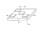
したがって、以下は、RFIDタグ200の基準となる向きを特定できるようにした構成例を説明する。かかるRFIDタグ200の第1の構成例を図2に示す。
図2に示すRFIDタグ200は、金属基体201の表面に電磁波吸収体202が4つ配置されており、このうち、隅部の3つの電磁波吸収体202が位置検出用のリファレンスポイントとして使用されることで、向きが特定される。例えば、金属基体201の縦および横のサイズや、リファレンスポイント(電磁波吸収体202)が配置されない金属基体201の一隅部の向き(例えば電磁波吸収体202の「右上側」である旨)をタグリーダー2に予め定義しておくことで、RFIDタグ200の向きを特定できる。
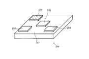
RFIDタグ200の第2の構成例を図3に示す。図3に示すRFIDタグ200は、図2と比較して分かるように、金属基体201の左上側の隅部の電磁波吸収体202を、電磁波反射率の異なる電磁波吸収体203に置換したものであり、他は図2と同一となっている。ここで、電磁波吸収体203の電磁波反射率は、電磁波吸収体202の電磁波反射率と20%以上異なっていることが望ましい。
このような構成とすることにより、図2の例と同一の平面パターンとしながら、互いを異なるものとして容易に判別することができる。したがって、本実施の形態のRFIDタグ200によれば、相互に同一のパターン形状であっても異なる識別情報を構成することで、高容量化を図ることができる。
図4から図8を参照して、RFIDタグ200を非金属製の容器の内部、例えば段ボール箱300の側面の内側に貼り付けて使用する場合を説明する。
本実施の形態では、プライバシー保護やタグ改ざん防止などの観点から、上述した遮蔽物に対する電磁波の透過性を利用して、図4Aに示すように、RFIDタグ200を段ボール箱300などの包装材(物品)の内部側面に貼り付けて使用することができる。すなわち、この場合、電磁波(送信波)を段ボール箱300の側面を通して(透過させて)RFIDタグ200に照射し、かつRFIDタグ200から反射される電磁波を段ボール箱300の側面を通して受信することができる。
ここで、RFIDタグ200を段ボール箱300の内部に貼り付ける場合、図4Bに示すように、電磁波吸収体202(203)の配置された側すなわち金属基体201の表面を、段ボール箱300の内側面に向けて貼り付けるとよい。なお、貼り付ける方法は、特に制限されず、例えば、接着剤、片面あるいは両面の粘着テープなどを使用することができ、以下の例も同様である。
段ボール箱300等の包装材を用いた物品の配送に関し、従来は、かかる包装材の外側に、物品受領者の住所、氏名、さらには物品の種類や値段など、種々の個人情報が記載された荷札が貼り付けられていたため、プライバシー等の観点からは問題があった。これに対し、本実施の形態によれば、RFIDタグ200に上記のような個人情報を含ませるとともに、かかるRFIDタグ200を段ボール箱300等の包装材の内部に貼り付けて使用することができるので、かかる個人情報を他者に知られないようにすることができる。
上述した各例は、電磁波吸収体202(203)を予め金属基体201に印刷することによりRFIDタグ200を構成(製造)した場合を説明した。他の例として、電磁波吸収体202(203)を印刷等により予め非金属製の物品に配置し、かかる物品に金属基体201を貼り付けてRFIDタグ200を構成(作成)してもよい。
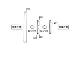
例えば、図5に示すように、上述した段ボール箱300の内側面に電磁波吸収体202を印刷しておき、印刷された電磁波吸収体202に金属基体201を貼り付けることにより、RFIDタグ200を構成(作成)することができる。
或いは、図6に示すように、非金属製(例えば、紙や木など)のシート材301に電磁波吸収体202(203)を印刷しておき、印刷された電磁波吸収体202に金属基体201を貼り付けることにより、RFIDタグ200を構成(作成)することができる。この場合、上述した段ボール箱300の内側面にシート材301を貼り付ければよい。
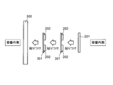
この場合、図7に示すように、シート材301の両面に電磁波吸収体202(または電磁波吸収体203)を印刷することで、RFIDタグ200における一部の電磁波吸収体を2層にして、他の電磁波吸収体に対して電磁波反射率を(望ましくは20%以上)異なるようにしてもよい。この場合、RFIDタグ200に担持させる識別情報の高容量化を図ることができる。
或いは、図8に示すように、電磁波吸収体202(または203)が印刷されたシート材301を多層にして、金属基体201および各シート材301を順次貼り付けてRFIDタグ200を構成(作成)してもよい。
図7や図8の構成例によれば、RFIDタグ200に担持させる識別情報の高容量化を図ることができる。
図6~図8に示す構成のより具体的な例としては、シート材301としてコピー用紙を使用し、電磁波吸収体202(203)としてカーボンブラックなどが含有されたトナーやインクを用いることができる。この場合、不図示のプリンタによってコピー用紙(シート材301)の上に、識別情報を構成するパターンを印刷(図7の例では両面印刷)すればよい。
上述のように、段ボール箱300の内側にRFIDタグ200を貼り付けて使用した場合、段ボール箱300を開封してRFIDタグ200を取り外さない限り、電磁波吸収体202(203)の配置パターンが他者に知られることがない。したがって、上記の使用方法によれば、物品受領者のプライバシー保護、悪意者による識別情報の改ざんのリスク軽減が図られる。
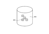
上述した各例は、金属基体201および電磁波吸収体202(203)によってRFIDタグ200を構成した場合を説明した。他の例として、RFIDタグ200は、金属基体201を用いずに、金属製の物品に電磁波吸収体202(203)を直接配置して構成することもできる。例えば、図9に示すように、アルミニウムや鉄などの金属製容器400の外面に電磁波吸収体202を印刷等で配置した場合でも、RFIDタグ200として機能することができる。
或いは、物品が金属部分を含む場合(例えば、金属製の筐体を有する各種物品のような場合)、かかる金属部分の表面に複数の電磁波吸収体202(203)をパターン化して配置したRFIDタグの構成とすることもできる。この場合、例えば、片面に粘着剤が付与された紙などの粘着シール上に電磁波吸収体202(203)のパターンを印刷し、配送の際に、かかる粘着シールを当該物品の金属部分に貼り付けることで、本実施の形態によるRFIDタグを作成する。
このようにすることで、物品の受領者が粘着シールを取り外すことで、使用時における物品の美観を損なうことがなく、また、個人情報の保護等を図ることができる。
さらには、図10Aおよび図10Bに示すように、RFIDタグ200を、受領者に配送される商品(内容物)とともに、非金属製(例えば紙、布、樹脂など)の包装袋500に入れ、または包装袋500自体に取り付け、かかる包装袋500を段ボール箱300に入れることも考えられる。本実施の形態によれば、このようにRFIDタグ200の表面の遮蔽が強化された場合であっても、タグリーダー2で電磁波の反射パターンを検出し、当該タグに構成された識別情報を読み取ることができる。また、この例では、包装袋500を開梱することなくタグリーダー2でRFIDタグ200の読み取りを行うことができるので、RFIDタグ200に商品名などの情報を含ませることにより、段ボール箱300に入れる内容物の誤認がないか等を配送業者側で確認することができる。
上述した各例は、複数の電磁波吸収体202を単一の金属体(金属基体201や容器等)の表面に配置したRFIDタグ200の構成例を説明した。RFIDタグ200の他の構成例として、この逆、すなわち、図11に示すように、単一の電磁波吸収体202の基体の表面に、複数の金属体204をパターン化して配置してもよい。
さらには、物品が電磁波吸収体を含む場合(例えば、物品が、カーボン製のシャフトや板状部などを有するスポーツ用品のような場合)、かかる電磁波吸収体の表面に複数の金属体204をパターン化して配置したRFIDタグの構成とすることもできる。この場合も、上述と同様に、例えば紙などの粘着シール上に金属体204をパターン化して設け、配送の際に、かかる粘着シールを当該物品の電磁波吸収体上に貼り付けることで、本実施の形態によるRFIDタグを作成することができる。この場合も、粘着シールが取り外されることで、使用時における物品の美観を損なうことがなく、また、個人情報の保護等を図ることができる。
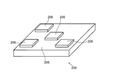
上述した各例は、電磁波吸収体と金属体との組み合わせによるRFIDタグ200の構成例を説明した。他の例として、電磁波反射率の異なる電磁波吸収体を組み合わせることによりRFIDタグ200を構成してもよい。具体例として、図12に示すRFIDタグ200は、第1の電磁波反射率を有する組成体による基体205の表面に、第2の電磁波反射率を有する組成体206が複数配置されている。
ここで、第1の電磁波反射率と第2の電磁波反射率との大小関係は任意であるが、上述した識別容易性の観点から、差異が20%以上であることが望ましい。
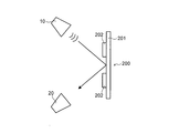
図13および図14を参照して、RFIDタグ200における電磁波(送信波)の反射の態様、および送信波の照射角度を広く確保するための構成について説明する。図13および図14では、タグリーダー2内の後述する電磁波送信部10および電磁波受信部20を抽出して示しており、RFIDタグ200の斜め方向から送信波が照射された場合を例示している。ここでは、上述した各構成例のうち、図2に示すRFIDタグ200を例示して説明するが、他の構成例でも同様の効果が得られる。
上述のように、本実施の形態で用いられる電磁波(送信波)は、直進性が高いことから、例えばRFIDタグ200の表面が鏡面のように滑らかな場合、電磁波送信部10から出力され金属基体201に当たった電磁波は、殆どが正反射の角度で反射する(図13参照)。したがって、RFIDタグ200に対して斜めの角度で電磁波を送受信するためには、図13に示すように電磁波送信部10および電磁波受信部20の位置を離す必要がある。他方、このような構成とすると、RFIDタグ200への送信波の入射角が小さい場合に電磁波受信部20で受信される信号強度が不十分になる虞がある。したがって、より一般的な使用方法である正面照射の態様を考慮すると、電磁波送信部10と電磁波受信部20は、互いに近い位置に設けた方がよいものと考えられる。
そこで、電磁波送信部10と電磁波受信部20とを近接配置しつつ、斜め照射にも対応するためには、RFIDタグ200の表面を、電磁波(送信波)が錯乱的に反射するような構成とするとよい。このような構成例としては、例えば図14に示すように、RFIDタグ200の表面(この例では金属基体201の表面)を粗くする(粗面とする)。このように、RFIDタグ200の表面を粗くすると、金属基体201に当たった電磁波を非正反射的に反射させること、すなわち送信波の入射角と異なった角度の反射波の成分を得ることができる。
この場合、送信波の一部が錯乱的に反射するため、図13の場合と比較して多少の損失が生じるが、送信波自体が十分な強度を有していることから、読み取り可能距離の減少を抑えながら反射波(受信信号)の強度を確保することができる。したがって、RFIDタグ200の表面を粗くすることにより、表面が滑らかな場合と比較して、電磁波送信部10と電磁波受信部20とを近接配置しつつ、送信波を照射する角度を広く確保することができる。
図12に示すRFIDタグ200の変形例を、図15を参照して説明する。図15に示すRFIDタグは、図12で上述した第2の電磁波反射率を有する組成体206の上に、かかる組成体206とは種類の異なる組成体207または組成体208が積層された構造となっている。具体的には、図12中、基体205の中央に配置された組成体206の上には組成体207が積層され、基体205の左上側に配置された組成体206の上には組成体208が積層されている。また、基体205の左および右下側に配置された組成体206の上には、各々、組成体207および組成体208がこの順で積層されている。
このような積層構造とすることにより、組成体206が配置された領域の電磁波反射率を適宜高めて、相互に同一のパターン形状であっても異なる識別情報を構成することで、高容量化を図ることができる。
次に、図16を参照して、上述したRFIDタグ200に構成された識別情報を読み取るためのタグリーダー2の構成を説明する。
タグリーダー2は、RFIDタグ200によって反射される電磁波の強弱パターンに基づいて識別情報を判別する判別装置としての機能を有し、図16に示すように、電磁波送信部10、電磁波受信部20、操作入力部30、表示部40、記憶部50、制御部100などを備える。
電磁波送信部10は、無線信号を生成するための電子回路や送信用のアンテナなどを備え、上述した10GHz~3THz(センチメートル波~ミリ波~遠赤外線)の範囲における所定周波数の電磁波を送信する電磁波送信機として機能する。
電磁波受信部20は、受信用のアンテナや電子回路等を備え、電磁波送信部10によって送信された電磁波の反射波の信号を受信する電磁波反射波受信機として機能する。電磁波受信部20は、RFIDタグ200の表面における電磁波の反射角度に対応した位置(図14等参照)に設けられている。電磁波受信部20は、受信された反射波の信号を制御部100に供給する。電磁波受信部20における受信感度のピーク点は、電磁波送信部10における送信周波数と同一の周波数に設定されている(図1Aおよび図1B参照)。
操作入力部30は、主電源のオンオフを行うための電源スイッチ、電磁波を出力(照射)するための照射スイッチ、などの各種スイッチ(操作ボタン)を備え、ユーザーによる各種入力操作を受け付けて、操作信号を制御部100に出力する。
表示部40は、例えば液晶ディスプレイ(LCD:Liquid Crystal Display)で構成される。表示部40は、制御部100から入力される表示制御信号に従って、各種操作画面や、RFIDタグ200に構成された識別情報を表示する。
制御部100は、CPU(Central Processing Unit)101、ROM(Read Only Memory)102、RAM(Random Access Memory)103等を備える。CPU101は、ROM102から処理内容に応じたプログラムを読み出してRAM103に展開し、展開したプログラムと協働してタグリーダー2の各ブロックの動作を制御する。このとき、記憶部50に格納されている各種データが参照される。記憶部50は、例えば不揮発性の半導体メモリ(いわゆるフラッシュメモリ)やハードディスクドライブで構成される。
制御部100は、電磁波受信部20から入力される反射波の信号を解析することによって、読み取りの対象となったRFIDタグ200の画像データを生成し、かかる画像データからRFIDタグ200に構成された識別情報を復号して表示する処理を実行する。
言い換えると、制御部100は、RFIDタグ200に照射された電磁波(送信波)の反射波の強弱状態(強弱パターン)から、送信波の反射情報(電磁波反射情報)を読み取る電磁波反射情報読取部として機能する。また、制御部100は、読み取った電磁波反射情報を画像情報に変換する画像情報変換部、変換された画像情報から識別情報を読み取る識別情報読取部、として機能する。
本実施の形態におけるタグリーダー2の使用方法を簡潔に述べる。タグリーダー2は、RFIDタグ200の方向に電磁波送信部10が向けられた後、照射スイッチが押されると電磁波送信部10から所定周波数の送信波(電磁波)が出力され、RFIDタグ200に照射される(図1A,図13,図14等参照)。そして、この電磁波がRFIDタグ200により反射され、電磁波受信部20により受信されると、上記さらには後述する種々の処理が行われることで、RFIDタグ200に構成された識別情報が読み取られ、かかる識別情報が表示部40に表示される。
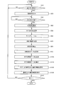
以下、図17のフローチャートを参照して、タグリーダー2の制御部100が行う処理の流れについて説明する。
電源投入後のステップS10において、制御部100は、操作入力部30からの入力信号を監視して、上記の照射スイッチ(以下、単にスイッチという。)が押圧されたか否かを判定する。制御部100は、スイッチが押圧されていない(ステップS10、NO)と判定した場合、前ステップに戻って当該判定を繰り返し行い、スイッチが押圧されたと判定すると(ステップS10、YES)、ステップS20に移行する。
ステップS20において、制御部100は、上述した送信波(電磁波)を出力するように電磁波送信部10に制御信号を出力する。かかる制御により、予め定められた周波数の電磁波が電磁波送信部10からRFIDタグ200に向けて出力(照射)される。
続くステップS30において、制御部100は、電磁波受信部20から入力される信号を監視して、当該出力した所定周波数の電磁波の反射波を受信したか否かを判定する。制御部100は、反射波が受信されていない(ステップS30、NO)と判定した場合、前ステップに戻って当該判定を繰り返し行い、反射波が受信されたと判定すると(ステップS30、YES)、ステップS40に移行する。
続いて、制御部100は、当該受信した反射波を解析し(ステップS40)、RFIDタグ200の向きを決定する(ステップS50)。かかる向きの決定は、例えば、RFIDタグ200の上述した複数のリファレンスポイントの各々の位置を特定することにより行われる。続いて、制御部100は、決定されたRFIDタグ200の向きに従ってキャリブレーションの処理を行う(ステップS60)。かかるキャリブレーションの処理は、例えば、各リファレンスポイントで反射した電磁波の反射率の値を基準値(例えば0)として設定するものである。
続いて、制御部100は、受信された反射波のうち、RFIDタグ200の方向における一定の領域(すなわちリファレンスポイントを端部とする矩形領域)について、X軸および直交するY軸の2次元平面を走査する(ステップS70)。また、制御部100は、かかる走査の結果から、RFIDタグ200の領域に対応する反射波の強度(強弱パターン、図1B参照)を検出する(ステップS80)。
続くステップS90において、制御部100は、当該検出された反射波のデータを記憶部50に保存し、ステップS100に移行する。
ステップS100において、制御部100は、RFIDタグ200の画像データを生成する。続くステップS110において、制御部100は、例えばエッジ処理や輝度補正などを施して、当該画像の輪郭をより鮮明にするように画像補正の処理を行う。かかる処理を行うことによって、読み取り対象となるRFIDタグ200の金属部分と電磁波吸収体の部分における輪郭、明度、濃淡等のコントラストがより明瞭になり、画像のパターン認識をより正確に行うことができる。
続いて、制御部100は、補正された画像のパターンから、当該RFIDタグ200により構成された識別情報を復号し(ステップS120)、復号された識別情報を表示部40に表示するように制御する(ステップS130)。
さらに、制御部100は、操作入力部30からの入力信号を監視して(ステップS140)、上述したスイッチの押圧が解除されたか否かを判定する。制御部100は、スイッチの押圧が解除されていない(すなわち押圧されたままである)と判定すると(ステップS140、NO)、ステップS10に戻り、上述した一連の処理を繰り返し行う。他方、制御部100は、スイッチの押圧が解除されたと判定すると(ステップS140、YES)、上述した一連の処理を終了する。
その他、上記実施の形態は、何れも本発明を実施するにあたっての具体化の一例を示したものに過ぎず、これらによって本発明の技術的範囲が限定的に解釈されてはならないものである。すなわち、本発明はその要旨、またはその主要な特徴から逸脱することなく、様々な形で実施することができる。
2017年7月12日出願の特願2017-136257の日本出願に含まれる明細書、図面および要約書の開示内容は、全て本願に援用される。
2 タグリーダー(判別装置)
10 電磁波送信部
20 電磁波受信部
30 操作入力部
40 表示部
100 制御部
200 RFIDタグ(非接触読み取りタグ)
201 金属基体
202,203 電磁波吸収体
204 金属体
205 組成体による基体
206,207,208 組成体
300 段ボール箱
301 シート材
400 金属製容器
500 包装袋
10 電磁波送信部
20 電磁波受信部
30 操作入力部
40 表示部
100 制御部
200 RFIDタグ(非接触読み取りタグ)
201 金属基体
202,203 電磁波吸収体
204 金属体
205 組成体による基体
206,207,208 組成体
300 段ボール箱
301 シート材
400 金属製容器
500 包装袋
Claims (20)
- 電磁波反射率の異なる複数の部材が識別情報に対応付けられたパターンで配置されており、
前記複数の部材に電磁波を照射した際に、該複数の部材によって反射される電磁波の強弱パターンに基づいて前記識別情報を判別可能である、
非接触読み取りタグ。 - 前記複数の部材の間では、前記電磁波反射率が20%以上異なっている、
請求項1に記載の非接触読み取りタグ。 - 前記複数の部材は、金属体、および電磁波吸収体を含む、
請求項1または2に記載の非接触読み取りタグ。 - 前記識別情報は、前記電磁波吸収体の種類、形および厚みの少なくとも1つに基づく情報である、
請求項3に記載の非接触読み取りタグ。 - 前記金属体の表面に前記電磁波吸収体が配置されている、
請求項3または4に記載の非接触読み取りタグ。 - 前記電磁波吸収体は、周波数が10GHz~3THzの電磁波に対する吸収性を有する材質を含む、
請求項3から5のいずれかに記載の非接触読み取りタグ。 - 前記電磁波吸収体は、磁性体、導電性材料、カーボン、無機微粒子、金属細線または樹脂を含む、
請求項3から6のいずれかに記載の非接触読み取りタグ。 - 前記電磁波吸収体は、前記金属体を含む物品上に配置されている、
請求項3から7のいずれかに記載の非接触読み取りタグ。 - 前記金属体は、前記電磁波吸収体を含む物品における電磁波吸収体上に取り付けられている、
請求項3から7のいずれかに記載の非接触読み取りタグ。 - 請求項1から7のいずれかに記載の非接触読み取りタグが取り付けられた物品。
- 請求項1から7のいずれかに記載の非接触読み取りタグと、
前記複数の部材に電磁波を照射した際に、該複数の部材によって反射される電磁波の強弱パターンに基づいて前記識別情報を判別する判別装置と、
を含む非接触読み取りタグシステム。 - 前記判別装置は、
前記非接触読み取りタグに向けて電磁波を送信する電磁波送信部と、
前記部材によって反射される電磁波を受信する電磁波受信部と、を含む、
請求項11に記載の非接触読み取りタグシステム。 - 前記電磁波受信部は、前記非接触読み取りタグの表面における前記電磁波の反射角度に対応した位置に設けられている、
請求項12に記載の非接触読み取りタグシステム。 - 前記非接触読み取りタグの表面は、前記電磁波を錯乱的に反射させる、
請求項13に記載の非接触読み取りタグシステム。 - 前記複数の部材は、金属体、および電磁波吸収体を含み、
前記電磁波吸収体の厚みは、前記電磁波送信部によって送信される電磁波の波長の1/4である、
請求項12から14のいずれかに記載の非接触読み取りタグシステム。 - 電磁波吸収体を含み電磁波反射率の異なる複数の部材が識別情報に対応付けられたパターンで配置される非接触読み取りタグの製造方法であって、
前記電磁波吸収体を印刷法によりパターニングする、
非接触読み取りタグの製造方法。 - 前記印刷法は、インクジェット印刷である、
請求項16に記載の非接触読み取りタグの製造方法。 - 前記電磁波吸収体を非金属の物品にパターニングし、
金属体を前記非金属の物品に貼り付ける、
請求項16または17に記載の非接触読み取りタグの製造方法。 - 電磁波吸収体を含み電磁波反射率の異なる複数の部材が識別情報に対応付けられたパターンで配置された非接触読み取りタグから前記識別情報を読み取る方法であって、
前記非接触読み取りタグに照射された電磁波の反射波から電磁波反射情報を読み取り、
前記電磁波反射情報を画像情報に変換し、
前記画像情報から前記識別情報を読み取る、
識別情報読み取り方法。 - 前記非接触読み取りタグにより反射された前記電磁波の強弱を読み取ることによって、前記電磁波反射情報を読み取る、
請求項19に記載の識別情報読み取り方法。
Applications Claiming Priority (2)
| Application Number | Priority Date | Filing Date | Title |
|---|---|---|---|
| JP2017-136257 | 2017-07-12 | ||
| JP2017136257 | 2017-07-12 |
Publications (1)
| Publication Number | Publication Date |
|---|---|
| WO2019012775A1 true WO2019012775A1 (ja) | 2019-01-17 |
Family
ID=65002493
Family Applications (1)
| Application Number | Title | Priority Date | Filing Date |
|---|---|---|---|
| PCT/JP2018/015889 Ceased WO2019012775A1 (ja) | 2017-07-12 | 2018-04-17 | 非接触読み取りタグ、非接触読み取りタグが取り付けられた物品、非接触読み取りタグシステム、非接触読み取りタグの製造方法、および識別情報読み取り方法 |
Country Status (1)
| Country | Link |
|---|---|
| WO (1) | WO2019012775A1 (ja) |
Cited By (3)
| Publication number | Priority date | Publication date | Assignee | Title |
|---|---|---|---|---|
| CN112417929A (zh) * | 2019-08-22 | 2021-02-26 | 阿里巴巴集团控股有限公司 | 一种物流对象识别方法、装置和系统 |
| JP2022038841A (ja) * | 2020-08-27 | 2022-03-10 | 富士フイルムビジネスイノベーション株式会社 | 記録材料及び記録媒体 |
| WO2025253957A1 (ja) * | 2024-06-04 | 2025-12-11 | 三菱重工機械システム株式会社 | パターン形成材、ケース、検出方法及び検出装置 |
Citations (3)
| Publication number | Priority date | Publication date | Assignee | Title |
|---|---|---|---|---|
| JP2011236271A (ja) * | 2010-05-06 | 2011-11-24 | Nhk Spring Co Ltd | 塗布剤、物品属性判別システム、物品属性判別方法および導体片 |
| JP2016018271A (ja) * | 2014-07-04 | 2016-02-01 | 大日本印刷株式会社 | コードパターンの認証方法および認証装置 |
| JP2016197295A (ja) * | 2015-04-02 | 2016-11-24 | 大日本印刷株式会社 | 識別用導電性部材、識別用導電性部材が設けられた物体の識別方法および識別装置 |
-
2018
- 2018-04-17 WO PCT/JP2018/015889 patent/WO2019012775A1/ja not_active Ceased
Patent Citations (3)
| Publication number | Priority date | Publication date | Assignee | Title |
|---|---|---|---|---|
| JP2011236271A (ja) * | 2010-05-06 | 2011-11-24 | Nhk Spring Co Ltd | 塗布剤、物品属性判別システム、物品属性判別方法および導体片 |
| JP2016018271A (ja) * | 2014-07-04 | 2016-02-01 | 大日本印刷株式会社 | コードパターンの認証方法および認証装置 |
| JP2016197295A (ja) * | 2015-04-02 | 2016-11-24 | 大日本印刷株式会社 | 識別用導電性部材、識別用導電性部材が設けられた物体の識別方法および識別装置 |
Cited By (3)
| Publication number | Priority date | Publication date | Assignee | Title |
|---|---|---|---|---|
| CN112417929A (zh) * | 2019-08-22 | 2021-02-26 | 阿里巴巴集团控股有限公司 | 一种物流对象识别方法、装置和系统 |
| JP2022038841A (ja) * | 2020-08-27 | 2022-03-10 | 富士フイルムビジネスイノベーション株式会社 | 記録材料及び記録媒体 |
| WO2025253957A1 (ja) * | 2024-06-04 | 2025-12-11 | 三菱重工機械システム株式会社 | パターン形成材、ケース、検出方法及び検出装置 |
Similar Documents
| Publication | Publication Date | Title |
|---|---|---|
| JP7147771B2 (ja) | 非接触読み取りタグ、非接触読み取りタグの製造方法、判別装置、および識別情報読み取り方法 | |
| US11487984B2 (en) | Contactlessly readable tag, method for manufacturing contactlessly readable tag, identification device, and identification information determination system | |
| US8830066B2 (en) | Package bag with externally attached communication device | |
| EP2248076B1 (en) | Rfid tag with a reduced read range | |
| US20080068132A1 (en) | Contactless radiofrequency device featuring several antennas and related antenna selection circuit | |
| WO2019012775A1 (ja) | 非接触読み取りタグ、非接触読み取りタグが取り付けられた物品、非接触読み取りタグシステム、非接触読み取りタグの製造方法、および識別情報読み取り方法 | |
| US20110227701A1 (en) | Gate system | |
| US20070024447A1 (en) | Radio energy propagation channel network for detecting RFID tagged items | |
| JP2008099266A (ja) | 通信改善装置、通信システムおよび物品情報取扱設備 | |
| JP2007118973A (ja) | コンテナボックス | |
| JP2023114292A (ja) | Rfタグシステム | |
| JP2010072957A (ja) | Rfidタグ | |
| WO2019065061A1 (ja) | チップレスrfidタグ、タグリーダー、及びrfidシステム | |
| JP4924379B2 (ja) | 非接触型icタグ及び非接触型icタグの製造方法 | |
| JP2019194825A (ja) | 非接触読み取りタグ、非接触読み取りタグの製造方法、判別装置及び識別情報判別システム | |
| CA2402683A1 (en) | Package identification system | |
| JP6894337B2 (ja) | 識別体 | |
| JP6464894B2 (ja) | 識別用導電性部材、識別用導電性部材が設けられた物体の識別方法および識別装置 | |
| EP4158542B1 (en) | Passive identification tags including resonant structures and characteristic layers | |
| Zeb et al. | Dual-polarized chipless humidity sensor tag | |
| CN202758374U (zh) | 可全方位读取的rfid电子标签及包装物 | |
| JP2013030877A (ja) | Rfid通信・人体通信併用通信構造 | |
| Kavčič et al. | Ultra-High Frequency Radio Frequency Identification Tag Antennas Printed Directly onto Cardboard used for the Manufacture of Pharmaceutical Packaging. | |
| US20080106418A1 (en) | RFID tag using patch antenna designs and low cost manufacturing techniques | |
| JP7590778B2 (ja) | Rfidタグ、パッシブ型rfidタグセンサー、rfidタグ用スペーサーおよび補助アンテナ用スペーサー |
Legal Events
| Date | Code | Title | Description |
|---|---|---|---|
| 121 | Ep: the epo has been informed by wipo that ep was designated in this application |
Ref document number: 18832010 Country of ref document: EP Kind code of ref document: A1 |
|
| NENP | Non-entry into the national phase |
Ref country code: DE |
|
| 122 | Ep: pct application non-entry in european phase |
Ref document number: 18832010 Country of ref document: EP Kind code of ref document: A1 |
|
| NENP | Non-entry into the national phase |
Ref country code: JP |