WO2019003952A1 - 分配器および合成器 - Google Patents
分配器および合成器 Download PDFInfo
- Publication number
- WO2019003952A1 WO2019003952A1 PCT/JP2018/022857 JP2018022857W WO2019003952A1 WO 2019003952 A1 WO2019003952 A1 WO 2019003952A1 JP 2018022857 W JP2018022857 W JP 2018022857W WO 2019003952 A1 WO2019003952 A1 WO 2019003952A1
- Authority
- WO
- WIPO (PCT)
- Prior art keywords
- phase adjustment
- output
- adjustment unit
- input
- unit
- Prior art date
- Legal status (The legal status is an assumption and is not a legal conclusion. Google has not performed a legal analysis and makes no representation as to the accuracy of the status listed.)
- Ceased
Links
Images







Classifications
-
- H—ELECTRICITY
- H01—ELECTRIC ELEMENTS
- H01P—WAVEGUIDES; RESONATORS, LINES, OR OTHER DEVICES OF THE WAVEGUIDE TYPE
- H01P3/00—Waveguides; Transmission lines of the waveguide type
- H01P3/02—Waveguides; Transmission lines of the waveguide type with two longitudinal conductors
- H01P3/08—Microstrips; Strip lines
- H01P3/088—Stacked transmission lines
-
- H—ELECTRICITY
- H01—ELECTRIC ELEMENTS
- H01P—WAVEGUIDES; RESONATORS, LINES, OR OTHER DEVICES OF THE WAVEGUIDE TYPE
- H01P5/00—Coupling devices of the waveguide type
- H01P5/12—Coupling devices having more than two ports
- H01P5/16—Conjugate devices, i.e. devices having at least one port decoupled from one other port
- H01P5/19—Conjugate devices, i.e. devices having at least one port decoupled from one other port of the junction type
-
- H—ELECTRICITY
- H01—ELECTRIC ELEMENTS
- H01P—WAVEGUIDES; RESONATORS, LINES, OR OTHER DEVICES OF THE WAVEGUIDE TYPE
- H01P1/00—Auxiliary devices
- H01P1/04—Fixed joints
- H01P1/047—Strip line joints
-
- H—ELECTRICITY
- H01—ELECTRIC ELEMENTS
- H01P—WAVEGUIDES; RESONATORS, LINES, OR OTHER DEVICES OF THE WAVEGUIDE TYPE
- H01P1/00—Auxiliary devices
- H01P1/18—Phase-shifters
-
- H—ELECTRICITY
- H01—ELECTRIC ELEMENTS
- H01P—WAVEGUIDES; RESONATORS, LINES, OR OTHER DEVICES OF THE WAVEGUIDE TYPE
- H01P1/00—Auxiliary devices
- H01P1/18—Phase-shifters
- H01P1/184—Strip line phase-shifters
-
- H—ELECTRICITY
- H01—ELECTRIC ELEMENTS
- H01P—WAVEGUIDES; RESONATORS, LINES, OR OTHER DEVICES OF THE WAVEGUIDE TYPE
- H01P3/00—Waveguides; Transmission lines of the waveguide type
- H01P3/02—Waveguides; Transmission lines of the waveguide type with two longitudinal conductors
- H01P3/08—Microstrips; Strip lines
-
- H—ELECTRICITY
- H01—ELECTRIC ELEMENTS
- H01P—WAVEGUIDES; RESONATORS, LINES, OR OTHER DEVICES OF THE WAVEGUIDE TYPE
- H01P5/00—Coupling devices of the waveguide type
- H01P5/12—Coupling devices having more than two ports
-
- H—ELECTRICITY
- H05—ELECTRIC TECHNIQUES NOT OTHERWISE PROVIDED FOR
- H05K—PRINTED CIRCUITS; CASINGS OR CONSTRUCTIONAL DETAILS OF ELECTRIC APPARATUS; MANUFACTURE OF ASSEMBLAGES OF ELECTRICAL COMPONENTS
- H05K1/00—Printed circuits
- H05K1/02—Details
- H05K1/0296—Conductive pattern lay-out details not covered by sub groups H05K1/02 - H05K1/0295
- H05K1/0298—Multilayer circuits
-
- H—ELECTRICITY
- H05—ELECTRIC TECHNIQUES NOT OTHERWISE PROVIDED FOR
- H05K—PRINTED CIRCUITS; CASINGS OR CONSTRUCTIONAL DETAILS OF ELECTRIC APPARATUS; MANUFACTURE OF ASSEMBLAGES OF ELECTRICAL COMPONENTS
- H05K1/00—Printed circuits
- H05K1/16—Printed circuits incorporating printed electric components, e.g. printed resistors, capacitors or inductors
Definitions
- the present technology relates to a distributor and a combiner, and more particularly to a distributor and a combiner that can realize miniaturization and low loss.
- Patent Document 1 a proposal has been made to configure a basic Wilkinson multi-splitter by wiring using VIA on a laminated substrate. According to this proposal, since four divisions can be realized by three layers and six divisions by five layers, the wiring length can be made shorter than a distributor realized by connecting two distribution circuits on a substrate in a tournament system.
- the present technology has been made in view of such a situation, and can achieve miniaturization and low loss.
- the distributor according to one aspect of the present technology is formed on a substrate and is connected to an external transmission line on the input side, an input branch unit, a distribution line that divides n paths from the input branch unit, and an output of the distribution line An output branch portion connected to the side and dividing the n distributed paths into an internal transmission line and an external transmission line on the output side; a coupling terminal coupling the n distributed paths on the inner side; the output branch And a phase adjustment unit arranged in series with a resistor and adjusting a phase between the connection unit and the coupling terminal, and phase rotation from the input branch to the output branch of each of the n distributed paths
- the quantity is ⁇ / 2 [rad]
- the amount of phase rotation from the output branch to the coupling terminal is a real multiple of ⁇ [rad] or ⁇ [rad].
- the phase adjustment unit is disposed between the output branch unit and the resistor.
- the phase adjustment unit is disposed between the resistor and the coupling terminal.
- the phase adjustment unit is composed of a first phase adjustment unit connected to the output branch unit, and a second phase adjustment unit connected to the coupling terminal, and the resistor is the first phase adjustment unit. And the second phase adjustment unit.
- the characteristic impedance Z 1 of the distribution line is designed as ⁇ (n Z in Z out ), and the resistance value R of the resistor is Z out .
- the characteristic impedance Z 2 of the phase adjustment unit is designed to be in the range of Z out / 2 ⁇ Z 2 ⁇ 2 * Z out .
- the phase adjustment unit is realized by a phase adjustment line in which the length from the input branch to the output branch is an integral multiple of ⁇ / 2 or ⁇ / 2.
- At least one of the distribution line and the phase adjustment unit includes one or more structures for connecting different planes, and the input branch unit and the coupling terminal are positioned on different planes.
- the input branch portion and the coupling terminal are on the same vertical line, and the distribution line, the phase adjustment portion, and the isolation resistor are arranged n-fold symmetrically with the vertical line as an axis.
- the combiner is formed on a substrate, connected to an external transmission line on the input side, and an input branch unit that divides the n paths into an internal side and a combined line, and the n paths
- An output combining unit that combines the combined lines divided into each and is connected to an external transmission line on the output side, a coupling terminal that couples the n paths on the inner side, the input branch unit and the coupling
- a phase adjustment unit is disposed between the terminal and the resistor in series connection to adjust the phase, and the phase rotation amount from the input branch unit to the output combining unit is n / 2 for each of the n pieces. rad], and the amount of phase rotation from the input branch to the coupling terminal is a real multiple of ⁇ [rad] or ⁇ [rad].
- the phase adjustment unit is disposed between the input branch unit and the resistor.
- the phase adjustment unit is disposed between the resistor and the coupling terminal.
- the phase adjustment unit includes a first phase adjustment unit connected to the input branch unit, and a second phase adjustment unit connected to the coupling terminal, and the resistor is the first phase adjustment unit. And the second phase adjustment unit.
- the characteristic impedance Z 1 of the combined line is designed as ⁇ (n Z in Z out ), and the resistance value R of the resistor is Z out .
- the characteristic impedance Z 2 of the phase adjustment unit is designed to be in the range of Z out / 2 ⁇ Z 2 ⁇ 2 * Z out .
- the phase adjustment unit is realized by a phase adjustment line whose length from the input branch unit to the output combining unit is an integral multiple of ⁇ / 2 or ⁇ / 2.
- At least one of the combined line and the phase adjusting unit includes one or more structures for connecting different planes, and the output combining unit and the coupling terminal are positioned on different planes.
- the output combining unit and the coupling terminal are on the same vertical line, and the combined line, the phase adjusting unit, and the resistance are arranged n-fold symmetrically with the vertical line as an axis.
- an input branch portion formed on a substrate and connected to an external transmission line on the input side, a distribution line that divides a path from the input branch portion into n, and an output side of the distribution line
- An output branch that divides the n-distributed paths into an external transmission line on the inner side and an output side; a coupling terminal that couples the n-distributed paths on the inner side; and the output branch
- a phase adjustment unit arranged in series with a resistor and adjusting a phase is provided between the connection terminal and the connection terminal.
- the amount of phase rotation from the input branch to the output branch of each of the n distributed paths is ⁇ / 2 [rad]
- the amount of phase rotation from the output branch to the coupling terminal is , ⁇ [rad] or real multiple of ⁇ [rad].
- an input branch unit formed on a substrate and connected to an external transmission line on the input side and divided into an inner side and a combined line every n paths, and each of the n paths
- An output combining unit coupled to the external transmission line on the output side, a coupling terminal for coupling the n paths on the inner side, the input branch unit and the coupling terminal
- a phase adjustment unit arranged in series with a resistor and adjusting the phase.
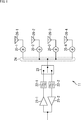
- FIG. 6 is an equivalent circuit diagram showing a first configuration example of a distributor / combiner.
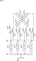
- FIG. 7 is an equivalent circuit diagram showing a second configuration example of a distributor / combiner.
- FIG. 7 is an equivalent circuit diagram showing a third configuration example of a distributor / combiner. It is a top view which shows the 1st structural example of a distributor / combiner. It is sectional drawing which shows the 1st structural example of a distributor / combiner.
- FIG. 6 is an equivalent circuit diagram showing a configuration example of the distributor / combiner of FIG. 5; It is a figure showing a simulation result. It is a figure showing a simulation result.
- FIG. 1 It is a figure which shows the example of the conventional 4 equal divider. It is a top view which shows the 2nd structural example of a distributor / combiner. It is sectional drawing which shows the 2nd structural example of a distributor / combiner. It is a top view which shows the 3rd structural example of a distributor / combiner. It is sectional drawing which shows the 3rd structural example of a distributor / combiner. It is a top view which shows the 4th structural example of a distributor / combiner. It is sectional drawing which shows the 4th structural example of a distributor / combiner. It is a block diagram which shows the structural example of a phase adjustment part.
- FIG. 1 shows a configuration example of a transmission / reception unit of a signal processing device to which the present technology is applied.
- FIG. 1 shows a configuration example of the transmission / reception unit 11 which is a front end module (FEM) of the signal processing apparatus.
- the transmission / reception unit 11 includes amplifiers 21-1 and 21-2, filters 22-1 and 22-2, a switch 23, a distributor / combiner 24, phase shifters 25-1 to 25-4, and antennas 26-1 to 26-4. It consists of 26-4.
- the amplifier 21-1 amplifies the signal from the signal processing unit and outputs the amplified signal to the filter 22-1.
- the amplifier 21-2 amplifies the signal from the filter 22-2 and outputs the amplified signal to a signal processing unit (not shown).
- the filter 22-1 applies a filter process to the signal from the amplifier 21-1 and outputs the signal subjected to the filter process to the switch 23.
- the filter 22-2 performs filter processing on the signal from the divider / combiner 24 input via the switch 23, and outputs the filtered signal to the amplifier 21-2.
- the switch 23 When transmitting a signal, the switch 23 selects the terminal on the filter 22-1 side, and outputs the signal from the terminal on the filter 22-1 side to the distributor / combiner 24. Further, when receiving a signal, the switch 23 selects the terminal on the filter 22-2 side, and outputs the signal from the divider / combiner 24 to the terminal on the filter 22-2 side.
- the divider / combiner 24 combines the signals from the phase shifters 25-1 to 25-4 and outputs the combined signal to the switch 23. Also, the distributor / combiner 24 distributes the signal from the switch 23 and outputs it to the phase shifters 25-1 to 25-4.
- the phase shifters 25-1 to 25-4 perform phase shift to match the phases of the signals from the antennas 26-1 to 26-4, and output the phase-shifted signals to the distributor / combiner 24.
- the phase shifters 25-1 to 25-4 respectively perform phase shift to shift the phase of the signal from the divider / combiner 24 little by little and output the phase-shifted signal to the antennas 26-1 to 26-4. Do.
- the antennas 26-1 to 26-4 are nondirectional antennas, and constitute a four-element antenna array.
- the antennas 26-1 to 26-4 each receive, for example, a signal from a base station of a radio wave, and output the received signal to the phase shifters 25-1 to 25-4. Also, the antennas 26-1 to 26-4 transmit the signals from the phase shifters 25-1 to 25-4 to the base station of the radio wave, respectively.
- FIG. 1 shows an example of four elements, other elements such as eight elements may be used. Also, in the example of FIG. 1, the filters 22-1 and 22-2 are disposed between the amplifiers 21-1 and 21-2 and the switch 23, but the divider / combiner 24 and the phase shifter 25- It may be arranged between 1 and 25-4.
- the amplifiers 21-1 and 21-2 will be collectively referred to as the amplifier 21 and the filters 22-1 and 22-2 will be collectively referred to as the filter 22 unless it is particularly necessary to distinguish.
- the phase shifters 25-1 to 25-4 are collectively referred to as a phase shifter 25 and the antennas 26-1 to 26-4 are collectively referred to as an antenna 26.
- FIG. 2 is an equivalent circuit diagram showing a first configuration example of the distributor / combiner 24. As shown in FIG.
- the distributor / combiner 24 is formed on a substrate.
- the distributor / combiner 24 includes an input / output terminal 51, an input branch 52, distribution lines 53-1 to 53-4, an output branch 54, phase adjusters 55-1 to 55-4, an isolation resistor 56-1 to 56-4, a coupling terminal 57, and input / output terminals 58-1 to 58-4.
- distribution lines 53-1 to 53-4 will be collectively referred to as a distribution line 53 and the phase adjustment units 55-1 to 55-8 will be collectively referred to as a phase adjustment unit 55, as appropriate, unless it is particularly necessary to distinguish.
- the input / output terminals 58-1 to 58-8 are collectively referred to as input / output terminals 58.
- the input / output terminal 51 inputs a signal from an external transmission line on the input side connected to the switch 23 to the input branch unit 52.
- the characteristic impedance at the input / output terminal 51 is referred to as an input impedance Z in .
- the input branch unit 52 connects the external transmission line on the input side and the distribution lines 53-1 to 53-4.
- Distribution lines 53-1 to 53-4 distribute the path from the input branch 52 into four.
- “Z 1 , ⁇ / 2” shown in the blocks of the distribution lines 53-1 to 53-4 in FIG. 2 are the characteristic impedance Z 1 of the distribution lines 53-1 to 53-4 and the phase rotation amount ⁇ , respectively. It is / 2 [rad].
- the amount of phase rotation of the distribution lines 53-1 to 53-4 represents the amount of phase rotation on the path from the input branch 52 to the output branch 54.
- the output branch unit 54 is connected to the output side of the distribution lines 53-1 to 53-4, and divides the four divided paths into an inner side path and an external transmission line on the output side.
- the path on the inner side represents a path connected to the phase adjustment units 55-1 to 55-4, the isolation resistors 56-1 to 56-4, and the coupling terminal 57.
- phase adjustment units 55-1 to 55-4 are disposed in front of isolation resistors 56-1 to 56-4, respectively, and are in series with isolation resistors 56-1 to 56-4. It is connected to the.
- Z 2 , ⁇ shown in the blocks of the phase adjustment units 55-1 to 55-4 in FIG. 2 are the characteristic impedance Z 2 of the phase adjustment units 55-1 to 55-4 and the phase rotation amount ⁇ , respectively. [rad] (or a real multiple of ⁇ [rad]).
- the amount of phase rotation of the phase adjusters 55-1 to 55-4 represents the amount of phase rotation on the path from the output branch 54 to the coupling terminal 57.
- the isolation resistors 56-1 to 56-4 are resistors for obtaining isolation characteristics between terminals.
- the type of isolation resistor may be any type such as a chip resistor or a thin film resistor.
- One terminals of the isolation resistors 56-1 to 56-4 are connected to the phase adjustment units 55-1 to 55-4, respectively, and the other terminals are connected to the common coupling terminal 57.
- the coupling terminal 57 couples the paths on the inner side connected to the isolation resistors 56-1 to 56-4.
- the input / output terminals 58-1 to 58-4 output the signals from the output branch 54 to external transmission lines connected to the antennas 26-1 to 26-4, respectively.
- the characteristic impedance at the input / output terminals 58-1 to 58-4 is taken as an output impedance Z out .
- the amount of phase rotation of the phase adjustment units 55-1 to 55-4 is a real number multiple of ⁇ [rad] or ⁇ [rad], respectively.
- the upper phase rotation amount is a real multiple of ⁇ [rad] or ⁇ [rad], respectively.
- the distributor is a Wilkinson distributor.
- phase adjustment unit 55-1 rotates the phase by a real number multiple of ⁇ [rad] or ⁇ [rad] in series with the isolation resistors 56-1 to 56-4 of the Wilkinson divider. Through 55-4 are added.
- the characteristic impedance Z 1 of the distribution line 53 is designed to be ⁇ (n Z in Z out ).
- the resistance value R of the isolation resistor 56 is designed to be Zout .
- the characteristic impedance Z 2 of the phase adjuster 55-1 to 55-4 what may be a value, but each to affect the frequency band and the wiring area, depending on the input and output impedances and distribution numbers Adjustment is necessary.
- the characteristic impedance Z 2 of the phase adjuster 55-1 to 55-4, Z out / 2 ⁇ Z 2 ⁇ 2 * Z out that is set to be in a value satisfying the condition, the relative bandwidth of about 10% ( Bandwidth of -20 dB) can be secured.
- the fractional bandwidth is the frequency resource, which is the ratio of the bandwidth to the center frequency.
- the signal flow is reversed, and the input side and the output side are opposite to the case of distribution. That is, the input / output terminal 51 is a terminal on the output side, and the input / output terminals 58-1 to 58-4 are terminals on the input side.
- the output branch 54 is an input branch
- the distribution line 53 is a combined line
- the input branch 52 is an output combiner
- the output branch unit (input branch unit) 54 is connected to the external transmission line on the input side via the input / output terminal 58 Ru.
- the output branch part (input branch part) 54 divides the path on the inner side and the distribution line (synthetic line) 53 every n paths.
- An input branch unit (output combining unit) 52 is connected to the output side of a distribution line (combined line) 53 divided into n paths, and connected to an external transmission line on the output side via an input / output terminal 51 Be done.
- the coupling terminal 57 couples n paths.
- the phase adjustment unit 55 is disposed between the output branch unit (input branch unit) 54 and the coupling terminal 57 so as to be connected in series with the isolation resistor 56, and adjusts the phase.
- phase rotation amount on the route from the output branch (input branch) 54 to the input branch (output combining unit) 52 is ⁇ / 2 [rad] for each of the n paths.
- amount of phase rotation on the path from the output branch (input branch) 54 to the coupling terminal 57 is a real multiple of ⁇ [rad] or ⁇ [rad].
- FIG. 2 the example in which the phase adjustment unit 55 is disposed in the front stage of the isolation resistor 56 has been described, with the input / output terminal 51 side as the front and the coupling terminal 57 side as the rear.
- the phase adjustment unit 55 may be disposed not on the front stage of the isolation resistor 56 but on the rear stage of the isolation resistor 56.
- FIG. 3 is an equivalent circuit diagram showing a second configuration example of the distributor / combiner 24. As shown in FIG.
- the equivalent circuit diagram of FIG. 3 is the same as the equivalent circuit diagram of FIG. 2 except that the position of the phase adjustment unit 55 and the position of the isolation resistor 56 are different.
- the other configuration of the equivalent circuit diagram of FIG. 3 is the same as the configuration of the equivalent circuit of FIG. 2, so only different portions will be described.
- phase adjustment unit 55 connected in series to the isolation resistor 56 is disposed downstream of the isolation resistor 56.
- the output branch unit 54 is connected to the output side of the distribution line 53, and divides the four divided paths into an inner side path and an external transmission line on the output side.
- the path on the inner side represents a path connected to the isolation resistor 56, the phase adjustment unit 55, and the coupling terminal 57.
- the isolation resistor 56 is disposed in the previous stage of the phase adjustment unit 55 and is connected in series to the phase adjustment unit 55.
- phase adjustment unit 55 One terminal of the phase adjustment unit 55 is connected to the isolation resistor 56, and the other terminal is connected to the common coupling terminal 57.
- Z 2 , ⁇ shown in the block of the phase adjustment unit 55 in FIG. 3 is the characteristic impedance Z 2 of the phase adjustment unit 55 and the phase rotation amount ⁇ [rad] (or a real multiple of ⁇ [rad]) is there.
- the isolation resistor 56 is wide, in the arrangement of FIG. 3, the output branch 54 may be wide, which may adversely affect the characteristics of the divider / combiner 24.
- the isolation resistor 56 may be disposed in the middle of the phase adjustment unit 55.
- FIG. 4 is an equivalent circuit diagram showing a third configuration example of the distributor / combiner 24. As shown in FIG. 4
- the equivalent circuit diagram of FIG. 4 is that the phase adjustment units 55-1 to 55-4 are configured by phase adjustment units 55a-1 to 55a-4 and phase adjustment units 55b-1 to 55b-4. It differs from the equivalent circuit diagram of Further, in the equivalent circuit diagram of FIG. 4, isolation resistors 56-1 to 56-4 are disposed between phase adjustment units 55a-1 to 55a-4 and phase adjustment units 55b-1 to 55b-4. The point is different from the equivalent circuit diagram of FIG.
- the other configuration of the equivalent circuit diagram of FIG. 4 is the same as the configuration of the equivalent circuit of FIG. 2, so only different portions will be described.
- phase adjustment units 55a-1 to 55a-4 are collectively referred to as a phase adjustment unit 55a
- phase adjustment units 55b-1 to 55b-4 are collectively referred to as a phase adjustment unit 55b, unless it is particularly necessary to distinguish.
- the output branch unit 54 is connected to the output side of the distribution line 53, and divides the four divided paths into an inner side path and an external transmission line on the output side.
- the path on the inner side represents a path connected to the phase adjustment unit 55 a, the isolation resistor 56, the phase adjustment unit 55 b, and the coupling terminal 57.
- phase adjustment unit 55 a In the path on the inner side, the phase adjustment unit 55 a is disposed in front of the isolation resistor 56.
- the phase adjustment unit 55 b is disposed downstream of the isolation resistor 56.
- phase adjustment unit 55a the isolation resistor 56, and the phase adjustment unit 55b are connected in series.
- Z 2 , ⁇ 1 shown in the block of the phase adjustment unit 55 a of FIG. 4 is the characteristic impedance Z 2 of the phase adjustment unit 55 a and the phase rotation amount ⁇ 1 [rad].
- Z 2 , ⁇ 2 shown in the block of the phase adjustment unit 55 b of FIG. 4 is the characteristic impedance Z 2 of the phase adjustment unit 55 b and the phase rotation amount ⁇ 2 [rad].
- One terminal of the phase adjustment unit 55 b is connected to the isolation resistor 56, and the other terminal is connected to the common coupling terminal 57.
- the position of the isolation resistor 56 may be between the phase adjustment units 55a and 55b, so either of the phase rotation amounts ⁇ 1 and ⁇ 2 may be larger.
- FIG. 4 shows an equivalent circuit
- the isolation resistor 56 is described as a lumped constant terminal having no size.
- the equivalent circuit of FIG. 4 is actually configured to be a real multiple of ⁇ [rad] or ⁇ [rad], including the phase rotation amount of the size of the resistance value R of the isolation resistor 56.
- the configuration as shown in FIG. 4 can improve the characteristics of the distributor / combiner 24 resulting from the wide width of the output branch 54.
- various configurations can be selected as the configuration of the distributor / combiner 24 according to the size of the isolation resistor 56 or the arrangement method of the phase adjustment unit 55.
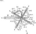
- FIG. 5 is a plan view schematically showing a structural example of the distributor / combiner 24.
- FIG. 6 is a plan view schematically showing an example of the layer structure of the distributor / combiner 24.
- FIG. 5 and 6 the same components as those described above are denoted by the same reference numerals. The same applies to FIG. 11 or later described later.
- FIG. 5 and FIG. 6 show a four equal distribution having a multi-layer substrate structure in which the distributor / combiner 24 is composed of three wiring layers constituting the first to third layers and one GND layer 81 in order from the bottom. / Shows an example configured as a synthesizer.
- the GND layer 81 is provided between the first layer and the second layer.
- phase adjusting units 55-1 to 55-4 are configured as phase adjusting lines 61-1 to 61-4.
- the external transmission line connected to the input / output terminal 51 is configured as the input transmission line 62
- the external transmission line connected to the input / output terminals 58-1 to 58-4 is the output transmission line 63-1 to 63. It is configured as -4.
- Each wiring is realized, for example, by a copper pattern on a FR 4 (Flame Retardant Type 4) substrate.
- VIA is used for wiring connection between layers.
- phase adjustment lines 61-1 to 61-4 are collectively referred to as the phase adjustment line 61
- output transmission lines 63-1 to 63-4 are collectively referred to as the output transmission line 63, unless it is particularly necessary to distinguish.
- the input branch 52 and the coupling terminal 57 are disposed at the same position in different layers.
- the phase adjustment line 61 is from the input branch 52 to the output branch 54 so that the length from the input branch 52 to the output branch 54 is ⁇ / 2 or an integral multiple thereof, where ⁇ is the wavelength of the signal.
- ⁇ is the wavelength of the signal.
- phase rotation amount in the path indicated by arrow # 11 from output branch 54 to coupling terminal 57 including phase adjustment line 61 and isolation resistor 56 is ⁇ [rad]. Or, it is formed so as to be a real multiple of ⁇ [rad].
- a path of a part of the input transmission line 62 is disposed in the first layer which is the lowermost layer.
- An input transmission line 62 is configured by the partial path disposed in the first layer and the VIA 71.
- the input transmission line 62 is connected to the distribution line 53 of the second layer at the input branching unit 52 via the VIA 71.
- a partial path of the distribution line 53 is disposed in the second layer.
- the distribution line 53 is configured by the partial path disposed in the second layer and the VIA 72.
- the distribution line 53 is connected to the third phase adjustment line 61 and the output transmission line 63 at the output branch 54 via the VIA 72.
- An output transmission line 63, a phase adjustment line 61, a coupling terminal 57, and an isolation resistor 56 are disposed in the third layer which is the uppermost layer.
- At least one of the distribution line 53 and the phase adjustment line 61 includes one or more structures (such as VIA) for connecting different planes (layers). Further, the input branch portion 52 and the coupling terminal 57 are located on different planes (layers).
- the input branch 52 and the coupling terminal 57 are on the same vertical line. Further, as shown in FIG. 5 with the vertical line as an axis, the distribution lines 53-1 to 53-4, the phase adjustment lines 61-1 to 61-4, and the isolation resistors 56-1 to 56-4 are It is arranged in four-fold symmetry.
- the n-fold symmetry represents an arrangement in which the same shape is obtained even when rotated 360 / n °.
- FIG. 7 is an equivalent circuit diagram of the divider / combiner 24 having the configuration of FIG. 5 and FIG.
- the input / output impedance is 50 ⁇
- the characteristic impedance of the phase adjustment unit 55 as the distribution line 53 and the phase adjustment line 61 is 100 ⁇ .
- the resistance value of the isolation resistor 56 is 50 ⁇ .
- a high frequency chip resistor of 0603 size (0.6 mm in length) or the like can be used as the isolation resistor 56.
- a thin film resistor by vapor deposition or an ink resistor may be used as the isolation resistor 56.
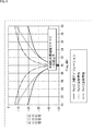
- ⁇ Simulation result> 8 and 9 are diagrams showing simulation results in the case of the equivalent circuit of FIG.
- Port1, Port2, and Port3 correspond to the input / output terminal 51, the input / output terminal 58-1, and the input / output terminal 58-2, respectively.
- the horizontal axis of FIG. 8 indicates the frequency, and the vertical axis indicates the pass characteristic of the signal of each frequency.
- the pass characteristic in the frequency of the path passing from the input / output terminal 51 which is Port 1 to the input / output terminal 58-1 which is Port 2 is shown by a broken line.
- the pass characteristic at the frequency of the path passing through the input / output terminal 51 is indicated by a solid line.
- the former pass characteristic indicated by a broken line overlaps the later pass characteristic indicated by a solid line.
- the pass characteristics are substantially flat, and it is understood that the pass characteristics at the time of distribution and at the time of combination are good in a wide band.
- the horizontal axis of FIG. 9 indicates the frequency, and the vertical axis indicates the characteristic of the signal of each frequency.
- the isolation characteristic between Port 2 and Port 3 is indicated by a solid line.
- the reflection characteristic of Port 1 is indicated by a broken line, and the reflection characteristic of Port 2 is indicated by a one-dot chain line.
- the distributor / combiner 24 has the necessary and sufficient characteristics as a four-way divider. It also has the necessary and sufficient characteristics as a 4th class synthesizer.
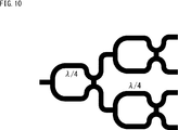
- the output from the input branch unit 52 is ⁇ / 4, it can be said that the size and the loss are small.
- the path is further extended in the conventional 8-equal divider disposed on the substrate, and the length between the input and the output is 3 ⁇ / 4. In the same way as in the 4-distribution case, ⁇ / 4 is sufficient.
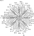
- FIG. 11 is a plan view schematically showing a structural example of the distributor / combiner 24.
- FIG. 12 is a cross-sectional view schematically showing an example of the layer structure of the distributor / combiner 24. As shown in FIG.
- the 11 and 12 each have a multi-layer substrate structure including the distributor / combiner 24 in the order from the bottom, the three wiring layers constituting the first to third layers, the two GND layers 81, and the GND layer 91.
- An example configured as an 8-equal distribution / combiner is shown.
- the GND layer 81 is provided between the first layer and the second layer.
- the GND layer 91 is provided between the second layer and the third layer.
- phase adjusting units 55-1 to 55-8 are configured as phase adjusting lines 61-1 to 61-8.
- an external transmission line connected to the input / output terminal 51 is configured as an input transmission line 62.
- the external transmission lines connected to the input / output terminals 58-1 to 58-8 are configured as output transmission lines 63-1 to 63-8.
- Each wiring is realized, for example, by a copper pattern on the FR4 substrate.
- VIA is used for the wiring connection between layers.
- phase adjustment units 55-1 to 55-8 are collectively referred to as a phase adjustment unit 55, and the input / output terminals 58-1 to 58-8 are collectively referred to as an input / output terminal 58, unless it is particularly necessary to distinguish.
- the phase adjustment lines 61-1 to 61-8 are collectively referred to as a phase adjustment line 61, and the output transmission lines 63-1 to 63-8 are collectively referred to as an output transmission line 63.
- the input branch portion 52 and the coupling terminal 57 are arranged at the same position where layers are different.
- the phase adjustment line 61 is from the input branch 52 to the output branch 54 so that the length from the input branch 52 to the output branch 54 is ⁇ / 2 or an integral multiple thereof, where ⁇ is the wavelength of the signal. Are connected in a substantially parabolic path.
- a path of a part of the input transmission line 62 is disposed in the first layer which is the lowermost layer.
- An input transmission line 62 is configured by the partial path disposed in the first layer and the VIA 71.
- the input transmission line 62 is connected to the distribution line 53 of the second layer at the input branching unit 52 via the VIA 71.
- a partial path of the distribution line 53 is disposed in the second layer.
- the distribution line 53 is configured by the partial path disposed in the second layer and the VIA 72.
- the distribution line 53 is connected to the third phase adjustment line 61 and the output transmission line 63 at the output branch 54 via the VIA 72.
- An output transmission line 63, a phase adjustment line 61, a coupling terminal 57, and an isolation resistor 56 are disposed in the third layer which is the uppermost layer.
- At least one of the distribution line 53 and the phase adjustment line 61 includes one or more structures (such as VIA) for connecting different planes (layers), and the input branch portion 52 and the coupling terminal 57 are different. It is located on a plane (layer).
- structures such as VIA
- the input branch 52 and the coupling terminal 57 are on the same vertical line. Further, as shown in FIG. 11, with the vertical line as an axis, the distribution lines 53-1 to 53-8, the phase adjustment lines 61-1 to 61-8, and the isolation resistors 56-1 to 56-8 are, It is arranged eight times symmetrically.
- FIG. 13 is a plan view schematically showing a structural example of the distributor / combiner 24.
- FIG. 14 is a cross-sectional view schematically showing an example of the layer structure of the distributor / combiner 24. As shown in FIG.
- FIGS. 13 and 14 show a GND VIA (GROUND VIA) connected to the GND layer 81 near the VIA connecting the second layer and the third layer in the first structure of the divider / combiner 24 of FIGS. 5 and 6.
- GND VIA GROUND VIA
- FIGS. 13 and 14 show a GND VIA (GROUND VIA) connected to the GND layer 81 near the VIA connecting the second layer and the third layer in the first structure of the divider / combiner 24 of FIGS. 5 and 6.
- GND VIA GROUND VIA
- the two GND VIAs 101-1 are disposed at a position sandwiching the VIA 72-1 as a center.
- the two GND VIAs 101-2 are arranged at the center of the VIA 72-2.
- the two GND VIAs 101-3 are disposed at a position sandwiching the VIA 72-3.
- the two GND VIAs 101-4 are disposed at a position sandwiching the VIA 72-4.
- the impedance mismatch due to the VIA can be mitigated, so reflection at the VIA can be suppressed and the pass characteristic can be improved.
- the GND VIA 101 is disposed near the VIA 72 connecting the second layer and the third layer. May be
- FIG. 15 is a plan view schematically showing a structural example of the distributor / combiner 24.
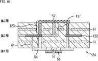
- FIG. 16 is a cross-sectional view schematically showing an example of the layer structure of the distributor / combiner 24. As shown in FIG.
- FIG. 15 and 16 show an example in which the layer structure of the distributor / combiner 24 of FIGS. 5 and 6 is changed.
- the description is abbreviate
- the input transmission lines 62-1 to 62-4 are replaced with the input transmission lines 121-1 to 121-4, and the output transmission lines 63-1 to 63-4 are output transmissions.
- the distribution lines 53-1 to 53-4 are replaced with the distribution lines 123-1 to 123-4 instead of the lines 122-1 to 122-4.
- the distributor / combiner 24 of FIGS. 15 and 16 is otherwise common to the distributor / combiner 24 of FIGS. 5 and 6.
- the input transmission lines 121-1 to 121-4 are collectively referred to as the input transmission line 121
- the output transmission lines 122-1 to 122-4 are collectively referred to as the output transmission line 122, unless it is particularly necessary to distinguish.
- the distribution lines 123-1 to 123-4 are collectively referred to as distribution lines 123.
- the distributor / combiner 24 shown in FIGS. 15 and 16 has a multi-layered substrate structure including the three wiring layers constituting the first to third layers, the two GND layers 81, and the GND layer 91 in order from the bottom 4
- An example configured as an equal distribution / combiner is shown.
- the GND layer 81 is provided between the first layer and the second layer.
- the GND layer 91 is provided between the second layer and the third layer.
- the input branch portion 52 and the coupling terminal 57 are arranged at the same position where layers are different.
- the phase adjustment line 61 is from the input branch 52 to the output branch 54 so that the length from the input branch 52 to the output branch 54 is ⁇ / 2 or an integral multiple thereof, where ⁇ is the wavelength of the signal. Are connected in a substantially parabolic path.
- phase adjustment line 61 is configured of a partial path and a path connecting the second layer and the third layer.
- the phase adjustment line 61 is connected to the output transmission line 122 of the second layer at the output branching unit 54 via a path connecting the second layer and the third layer.
- a part of the path of the input transmission line 121 and the output transmission line 122 are formed by strip lines.
- the input transmission line 121 is configured by a part of paths and paths connecting the third layer and the second layer.
- the input transmission line 121 is connected to the distribution line 123 of the third layer at the input branch unit 52 via a path connecting the third layer and the second layer.
- a part of the distribution line 123 is formed of a microstrip line.
- the distribution line 123 is configured by a part of paths and vias connecting the third layer and the second layer.
- the distribution line 123 is connected to the output transmission line 122 of the second layer at the output branch 54 through the via.
- both the input transmission line 121 and the output transmission line 122 are often 50 ⁇ .
- the distribution line 123 needs to have a characteristic impedance higher than that of the input transmission line 121 and the output transmission line 122 so as to be 100 ⁇ by four distribution. If these transmission lines are mounted on the same plane, it may be a design with a line width that is difficult to realize.
- the input transmission line 121 and the output transmission line 122 are designed with strip lines which are likely to have a relatively low impedance.
- the distribution line 123 can be designed as a microstrip line which has the same line width and higher impedance than the strip line. From the above, it is possible to design with a sufficiently achievable line width.
- phase adjusting unit 55 may be configured as the phase adjusting line 61.
- FIG. 17 is a block diagram showing a configuration example of the phase adjustment unit 55. As shown in FIG. 17
- the phase adjustment unit 55 of FIG. 17 is configured of a transmission line 151 of an arbitrary phase rotation amount ⁇ and a delay circuit configured of a lumped constant.
- FIG. 17A shows an example in which the lumped constant is an HPF (High Pass Filter) 152 comprising capacitors 161-1 and 161-2 and a coil 162.
- HPF High Pass Filter
- FIG. 17B shows an example in which the lumped constant is an LPF (Low Pass Filter) 153 composed of the coils 171-1 and 171-2 and a capacitor 172.
- LPF Low Pass Filter
- the impedance characteristics Z 2 in the transmission line 151 whatever good, select the value of the lumped constant for any theta, it is possible consistent.
- ⁇ [rad] or ⁇ [rad] can be adjusted to real multiples.
- the phase adjustment unit 55 is not limited to the one described above, and any phase adjustment unit may be used as long as it adjusts the phase.
- the phase adjustment unit connected in series with the resistor is provided. Therefore, even if the size of the VIA or the resistor is not sufficiently small with respect to the wavelength, the design can be performed without losing the isolation characteristics. It is.
- the phase adjustment unit since the phase adjustment unit has a size, the degree of freedom in mounting the isolation resistor is increased, so that the substrate can be mounted with a reasonable structure.
- the present technology is also applied to a distributor / combiner, a distributor, and a synthesizer, and a mobile phone, a smart phone, a tablet terminal, a personal computer, a mobile terminal, and the like including the same.
- the present technology can also have the following configurations.
- An input branch connected to an external transmission line on the input side;
- a distribution line that divides the path from the input branch into n parts;
- An output branch unit connected to the output side of the distribution line and dividing an n-distributed path into an internal transmission line and an output side external transmission line;
- a coupling terminal for coupling the n distributed paths on the inner side;
- a phase adjustment unit arranged in series with a resistor and adjusting a phase between the output branch unit and the coupling terminal;
- the amount of phase rotation from the input branch to the output branch of each of the n distributed paths is ⁇ / 2 [rad]
- the amount of phase rotation from the output branch to the coupling terminal is a real multiple of ⁇ [rad] or ⁇ [rad], including the magnitude of the resistance.
- the phase adjustment unit includes a first phase adjustment unit connected to the output branch unit, and a second phase adjustment unit connected to the coupling terminal.
- Characteristic impedance Z 2 of the phase adjustment unit Distributor according to (5) which is designed to be Z out / 2 ⁇ Z range of 2 ⁇ 2 * Z out.
- the phase adjustment unit is realized by a phase adjustment line in which the length from the input branch unit to the output branch unit is an integral multiple of ⁇ / 2 or ⁇ / 2. Distributor described in.
- At least one of the distribution line and the phase adjustment unit includes one or more structures connecting between different planes, The distributor according to any one of (1) to (7), wherein the input branch portion and the coupling terminal are configured to be located on different planes.
- the input branch and the coupling terminal are on the same vertical line, The distributor according to (8), wherein the distribution line, the phase adjustment unit, and the isolation resistance are arranged n-fold symmetrically with the vertical line as an axis.
- the amount of phase rotation from the input branch unit to the output combining unit is ⁇ / 2 [rad] for each of the n pieces,
- the amount of phase rotation from the input branch to the coupling terminal is a real multiple of ⁇ [rad] or ⁇ [rad].
- the characteristic impedance Z 1 of the combined line is ⁇ (n Z in Z out ), wherein the resistance value R of the resistor is, the synthesizer according to any one of the above is designed with Z out (10) to (13).
- Characteristic impedance Z 2 of the phase adjustment unit Synthesizer according to the above (14) which is designed to be Z out / 2 ⁇ Z range of 2 ⁇ 2 * Z out.
- the phase adjustment unit is realized by a phase adjustment line in which the length from the input branch unit to the output combining unit is an integral multiple of ⁇ / 2 or ⁇ / 2. Any of the above (10) to (15) Synthesizer described in.
- At least one of the combined line and the phase adjustment unit includes one or more structures for connecting different planes, The combiner according to any one of (10) to (16), wherein the output combining unit and the coupling terminal are configured to be located on different planes. (18) The output combining unit and the coupling terminal are on the same vertical line, The combiner according to (17), wherein the combined line, the phase adjustment unit, and the resistance are arranged n-fold symmetrically with the vertical line as an axis.
Landscapes
- Engineering & Computer Science (AREA)
- Microelectronics & Electronic Packaging (AREA)
- Amplifiers (AREA)
- Variable-Direction Aerials And Aerial Arrays (AREA)
Abstract
Description
1.信号処理装置の一部の構成例
2.分配/合成器の構成例
3.分配/合成器の第1の構造例
4.シミュレーション結果
5.分配/合成器の第2の構造例
6.分配/合成器の第3の構造例
7.分配/合成器の第4の構造例
8.位相調整部の構成例
図1は、本技術を適用した信号処理装置の送受信部の構成例を示している。
図2は、分配/合成器24の第1の構成例を示す等価回路図である。
次に、図5および図6を参照して、分配/合成器24の第1の構造について説明する。
図8および図9は、図7の等価回路の場合のシミュレーション結果を表す図である。
次に、図11および図12を参照して、分配/合成器24の第2の構造について説明する。
次に、図13および図14を参照して、分配/合成器24の第3の構造について説明する。
次に、図15および図16を参照して、分配/合成器24の第4の構造について説明する。
図17は、位相調整部55の構成例を示すブロック図である。
(1)
基板に形成され、
入力側の外部伝送線路と接続される入力分岐部と、
前記入力分岐部からの経路をn分配する分配線路と、
前記分配線路の出力側と接続され、n分配された経路を、内部側と出力側の外部伝送線路とに分ける出力分岐部と、
前記内部側において、前記n分配された経路を結合する結合端子と、
前記出力分岐部と前記結合端子との間に、抵抗と直列接続で配置され、位相を調整する位相調整部と
を備え、
前記n分配された経路それぞれの前記入力分岐部から前記出力分岐部までの位相回転量は、π/2[rad]であり、
前記出力分岐部から前記結合端子までの位相回転量は、前記抵抗の大きさを含めて、π[rad]またはπ[rad]の実数倍である
分配器。
(2)
前記位相調整部は、前記出力分岐部と前記抵抗との間に配置される
前記(1)に記載の分配器。
(3)
前記位相調整部は、前記抵抗と前記結合端子との間に配置される
前記(1)に記載の分配器。
(4)
前記位相調整部は、前記出力分岐部と接続される第1の位相調整部と、前記結合端子と接続される第2の位相調整部とで構成され、
前記抵抗は、前記第1の位相調整部と前記第2の位相調整部との間に配置される
前記(1)に記載の分配器。
(5)
入力インピーダンスZin、出力インピーダンスZout、分配数nのとき、
前記分配線路の特性インピーダンスZ1が、√(n Zin Zout)、
前記抵抗の抵抗値Rが、Zoutで設計されている
前記(1)乃至(4)のいずれかに記載の分配器。
(6)
前記位相調整部の特性インピーダンスZ2が、
Zout/2 ≦ Z2 ≦ 2*Zoutの範囲になるように設計されている
前記(5)に記載の分配器。
(7)
前記位相調整部が、前記入力分岐部から前記出力分岐部までの長さがλ/2またはλ/2の整数倍となる位相調整線路によって実現されている
前記(1)乃至(6)のいずれかに記載の分配器。
(8)
前記分配線路および前記位相調整部の少なくとも一方に、異なる平面間を接続する構造を1ヶ所以上含み、
前記入力分岐部と前記結合端子とが異なる平面上に位置するように構成される
前記(1)乃至(7)のいずれかに記載の分配器。
(9)
前記入力分岐部と前記結合端子が同一鉛直線上にあり、
前記鉛直線を軸として、前記分配線路、前記位相調整部、前記アイソレーション抵抗がn回対称に配置されている
前記(8)に記載の分配器。
(10)
基板に形成され、
入力側の外部伝送線路と接続され、n本の経路毎に内部側と合成線路とに分ける入力分岐部と、
前記n本の経路毎に分けられた合成線路を合成し、出力側の外部伝送線路と接続される出力合成部と、
前記内部側において、前記n本の経路を結合する結合端子と、
前記入力分岐部と前記結合端子との間に抵抗と直列接続で配置され、位相を調整する位相調整部と
を備え、
前記n本のそれぞれについて、前記入力分岐部から出力合成部までの位相回転量は、π/2[rad]であり、
前記入力分岐部から前記結合端子までの位相回転量は、π[rad]またはπ[rad]の実数倍である
合成器。
(11)
前記位相調整部は、前記入力分岐部と前記抵抗との間に配置される
前記(10)に記載の合成器。
(12)
前記位相調整部は、前記抵抗と前記結合端子との間に配置される
前記(10)に記載の合成器。
(13)
前記位相調整部は、前記入力分岐部と接続される第1の位相調整部と、前記結合端子と接続される第2の位相調整部とで構成され、
前記抵抗は、前記第1の位相調整部と前記第2の位相調整部との間に配置される
前記(10)に記載の合成器。
(14)
入力インピーダンスZin、出力インピーダンスZout、分配数nのとき、
前記合成線路の特性インピーダンスZ1が、√(n Zin Zout)、
前記抵抗の抵抗値Rが、Zoutで設計されている
前記(10)乃至(13)のいずれかに記載の合成器。
(15)
前記位相調整部の特性インピーダンスZ2が、
Zout/2 ≦ Z2 ≦ 2*Zoutの範囲になるように設計されている
前記(14)に記載の合成器。
(16)
前記位相調整部が、前記入力分岐部から前記出力合成部までの長さがλ/2またはλ/2の整数倍となる位相調整線路によって実現されている
前記(10)乃至(15)のいずれかに記載の合成器。
(17)
前記合成線路および前記位相調整部の少なくとも一方に、異なる平面間を接続する構造を1ヶ所以上含み、
前記出力合成部と前記結合端子とが異なる平面上に位置するように構成される
前記(10)乃至(16)のいずれかに記載の合成器。
(18)
前記出力合成部と前記結合端子が同一鉛直線上にあり、
前記鉛直線を軸として、前記合成線路、前記位相調整部、前記抵抗がn回対称に配置されている
前記(17)に記載の合成器。
Claims (18)
- 基板に形成され、
入力側の外部伝送線路と接続される入力分岐部と、
前記入力分岐部からの経路をn分配する分配線路と、
前記分配線路の出力側と接続され、n分配された経路を、内部側と出力側の外部伝送線路とに分ける出力分岐部と、
前記内部側において、前記n分配された経路を結合する結合端子と、
前記出力分岐部と前記結合端子との間に、抵抗と直列接続で配置され、位相を調整する位相調整部と
を備え、
前記n分配された経路それぞれの前記入力分岐部から前記出力分岐部までの位相回転量は、π/2[rad]であり、
前記出力分岐部から前記結合端子までの位相回転量は、前記抵抗の大きさを含めて、π[rad]またはπ[rad]の実数倍である
分配器。 - 前記位相調整部は、前記出力分岐部と前記抵抗との間に配置される
請求項1に記載の分配器。 - 前記位相調整部は、前記抵抗と前記結合端子との間に配置される
請求項1に記載の分配器。 - 前記位相調整部は、前記出力分岐部と接続される第1の位相調整部と、前記結合端子と接続される第2の位相調整部とで構成され、
前記抵抗は、前記第1の位相調整部と前記第2の位相調整部との間に配置される
請求項1に記載の分配器。 - 入力インピーダンスZin、出力インピーダンスZout、分配数nのとき、
前記分配線路の特性インピーダンスZ1が、√(n Zin Zout)、
前記抵抗の抵抗値Rが、Zoutで設計されている
請求項1に記載の分配器。 - 前記位相調整部の特性インピーダンスZ2が、
Zout/2 ≦ Z2 ≦ 2*Zoutの範囲になるように設計されている
請求項5に記載の分配器。 - 前記位相調整部が、前記入力分岐部から前記出力分岐部までの長さがλ/2またはλ/2の整数倍となる位相調整線路によって実現されている
請求項1に記載の分配器。 - 前記分配線路および前記位相調整部の少なくとも一方に、異なる平面間を接続する構造を1ヶ所以上含み、
前記入力分岐部と前記結合端子とが異なる平面上に位置するように構成される
請求項1に記載の分配器。 - 前記入力分岐部と前記結合端子が同一鉛直線上にあり、
前記鉛直線を軸として、前記分配線路、前記位相調整部、前記抵抗がn回対称に配置されている
請求項8に記載の分配器。 - 基板に形成され、
入力側の外部伝送線路と接続され、n本の経路毎に内部側と合成線路とに分ける入力分岐部と、
前記n本の経路毎に分けられた合成線路を合成し、出力側の外部伝送線路と接続される出力合成部と、
前記内部側において、前記n本の経路を結合する結合端子と、
前記入力分岐部と前記結合端子との間に抵抗と直列接続で配置され、位相を調整する位相調整部と
を備え、
前記n本のそれぞれについて、前記入力分岐部から出力合成部までの位相回転量は、π/2[rad]であり、
前記入力分岐部から前記結合端子までの位相回転量は、π[rad]またはπ[rad]の実数倍である
合成器。 - 前記位相調整部は、前記入力分岐部と前記抵抗との間に配置される
請求項10に記載の合成器。 - 前記位相調整部は、前記抵抗と前記結合端子との間に配置される
請求項10に記載の合成器。 - 前記位相調整部は、前記入力分岐部と接続される第1の位相調整部と、前記結合端子と接続される第2の位相調整部とで構成され、
前記抵抗は、前記第1の位相調整部と前記第2の位相調整部との間に配置される
請求項10に記載の合成器。 - 入力インピーダンスZin、出力インピーダンスZout、分配数nのとき、
前記合成線路の特性インピーダンスZ1が、√(n Zin Zout)、
前記抵抗の抵抗値Rが、Zoutで設計されている
請求項10に記載の合成器。 - 前記位相調整部の特性インピーダンスZ2が、
Zout/2 ≦ Z2 ≦ 2*Zoutの範囲になるように設計されている
請求項14に記載の合成器。 - 前記位相調整部が、前記入力分岐部から前記出力合成部までの長さがλ/2またはλ/2の整数倍となる位相調整線路によって実現されている
請求項10に記載の合成器。 - 前記合成線路および前記位相調整部の少なくとも一方に、異なる平面間を接続する構造を1ヶ所以上含み、
前記出力合成部と前記結合端子とが異なる平面上に位置するように構成される
請求項10に記載の合成器。 - 前記出力合成部と前記結合端子が同一鉛直線上にあり、
前記鉛直線を軸として、前記合成線路、前記位相調整部、前記抵抗がn回対称に配置されている
請求項17に記載の合成器。
Priority Applications (4)
| Application Number | Priority Date | Filing Date | Title |
|---|---|---|---|
| CN201880041741.0A CN110809835B (zh) | 2017-06-29 | 2018-06-15 | 分配器和合成器 |
| KR1020197035689A KR20200016851A (ko) | 2017-06-29 | 2018-06-15 | 분배기 및 합성기 |
| US16/626,301 US11217871B2 (en) | 2017-06-29 | 2018-06-15 | Distributor and synthesizer |
| DE112018003343.0T DE112018003343B4 (de) | 2017-06-29 | 2018-06-15 | Verteiler und synthetisierer |
Applications Claiming Priority (2)
| Application Number | Priority Date | Filing Date | Title |
|---|---|---|---|
| JP2017127020A JP2019012877A (ja) | 2017-06-29 | 2017-06-29 | 分配器および合成器 |
| JP2017-127020 | 2017-06-29 |
Publications (1)
| Publication Number | Publication Date |
|---|---|
| WO2019003952A1 true WO2019003952A1 (ja) | 2019-01-03 |
Family
ID=64740568
Family Applications (1)
| Application Number | Title | Priority Date | Filing Date |
|---|---|---|---|
| PCT/JP2018/022857 Ceased WO2019003952A1 (ja) | 2017-06-29 | 2018-06-15 | 分配器および合成器 |
Country Status (6)
| Country | Link |
|---|---|
| US (1) | US11217871B2 (ja) |
| JP (1) | JP2019012877A (ja) |
| KR (1) | KR20200016851A (ja) |
| CN (1) | CN110809835B (ja) |
| DE (1) | DE112018003343B4 (ja) |
| WO (1) | WO2019003952A1 (ja) |
Families Citing this family (2)
| Publication number | Priority date | Publication date | Assignee | Title |
|---|---|---|---|---|
| WO2023154038A1 (en) * | 2022-02-09 | 2023-08-17 | Fujikura Ltd. | Splitter-combiner and cascade connection circuit |
| US12283733B2 (en) * | 2023-04-13 | 2025-04-22 | Radio Wires Inc. | Multi-tap transmission line system and methods thereof |
Citations (6)
| Publication number | Priority date | Publication date | Assignee | Title |
|---|---|---|---|---|
| JPS49128142U (ja) * | 1973-03-01 | 1974-11-02 | ||
| JPS5573119A (en) * | 1978-11-27 | 1980-06-02 | Toshiba Corp | Distributing compounder |
| JPH02203604A (ja) * | 1989-02-02 | 1990-08-13 | Fujitsu Ltd | 3分岐同相ハイブリッド |
| JPH09321509A (ja) * | 1996-03-26 | 1997-12-12 | Matsushita Electric Ind Co Ltd | 分配器/合成器 |
| JPH11340712A (ja) * | 1998-05-26 | 1999-12-10 | Toshiba Corp | 高周波電力分配器 |
| JP2013502874A (ja) * | 2009-08-24 | 2013-01-24 | レイセオン カンパニー | 多層の放射状電力分割器/結合器 |
Family Cites Families (11)
| Publication number | Priority date | Publication date | Assignee | Title |
|---|---|---|---|---|
| US5021755A (en) * | 1989-11-08 | 1991-06-04 | Radio Frequency Systems, Inc. | N-way signal splitter with isolated outputs |
| KR100279490B1 (ko) * | 1996-08-12 | 2001-02-01 | 김덕용 | N-웨이 전력 분배기/합성기 |
| JP3811551B2 (ja) | 1997-09-17 | 2006-08-23 | 松下電器産業株式会社 | 高出力電力増幅器 |
| US7164903B1 (en) * | 2003-06-10 | 2007-01-16 | Smiths Interconnect Microwave Components, Inc. | Integrated N-way Wilkinson power divider/combiner |
| FI119710B (fi) * | 2004-03-22 | 2009-02-13 | Filtronic Comtek Oy | Pienikohinaisen vahvistinparin tulojärjestely |
| JP4056500B2 (ja) * | 2004-06-28 | 2008-03-05 | 三菱電機株式会社 | 伝送線路基板および半導体パッケージ |
| CN101465457B (zh) * | 2009-01-15 | 2012-11-21 | 电子科技大学 | 一种高功率宽带四路功率分配、合成器 |
| WO2012003506A2 (en) * | 2010-07-02 | 2012-01-05 | Nuvotronics, Llc | Three-dimensional microstructures |
| US8941448B2 (en) * | 2011-10-13 | 2015-01-27 | Mediatek Singapore Pte. Ltd. | M-way coupler |
| CN103943930B (zh) | 2014-05-13 | 2016-06-15 | 苏州博海创业微系统有限公司 | 一种ltcc多路平衡功分器 |
| CN104051822B (zh) * | 2014-05-28 | 2017-08-25 | 西安电子科技大学 | 一种用于四臂螺旋天线馈电的功分移相器 |
-
2017
- 2017-06-29 JP JP2017127020A patent/JP2019012877A/ja active Pending
-
2018
- 2018-06-15 US US16/626,301 patent/US11217871B2/en active Active
- 2018-06-15 KR KR1020197035689A patent/KR20200016851A/ko not_active Abandoned
- 2018-06-15 WO PCT/JP2018/022857 patent/WO2019003952A1/ja not_active Ceased
- 2018-06-15 DE DE112018003343.0T patent/DE112018003343B4/de not_active Expired - Fee Related
- 2018-06-15 CN CN201880041741.0A patent/CN110809835B/zh not_active Expired - Fee Related
Patent Citations (6)
| Publication number | Priority date | Publication date | Assignee | Title |
|---|---|---|---|---|
| JPS49128142U (ja) * | 1973-03-01 | 1974-11-02 | ||
| JPS5573119A (en) * | 1978-11-27 | 1980-06-02 | Toshiba Corp | Distributing compounder |
| JPH02203604A (ja) * | 1989-02-02 | 1990-08-13 | Fujitsu Ltd | 3分岐同相ハイブリッド |
| JPH09321509A (ja) * | 1996-03-26 | 1997-12-12 | Matsushita Electric Ind Co Ltd | 分配器/合成器 |
| JPH11340712A (ja) * | 1998-05-26 | 1999-12-10 | Toshiba Corp | 高周波電力分配器 |
| JP2013502874A (ja) * | 2009-08-24 | 2013-01-24 | レイセオン カンパニー | 多層の放射状電力分割器/結合器 |
Non-Patent Citations (1)
| Title |
|---|
| GYSEL: "A NEW N-WAY POWER DIVIDER/COMBINERSUTABLE FOR HIGH- POWER APPLICATIONS", IEEE -MTT-S INTERNATIONAL MICROWAVE SYMPOSIUM, 12 May 1975 (1975-05-12), pages 116 - 118, XP031665948 * |
Also Published As
| Publication number | Publication date |
|---|---|
| DE112018003343T5 (de) | 2020-03-05 |
| JP2019012877A (ja) | 2019-01-24 |
| DE112018003343B4 (de) | 2026-01-29 |
| CN110809835A (zh) | 2020-02-18 |
| US11217871B2 (en) | 2022-01-04 |
| US20200161737A1 (en) | 2020-05-21 |
| CN110809835B (zh) | 2021-11-19 |
| KR20200016851A (ko) | 2020-02-17 |
Similar Documents
| Publication | Publication Date | Title |
|---|---|---|
| JP6881675B2 (ja) | アンテナモジュール | |
| JP5083987B2 (ja) | 不均等3分配器 | |
| US20160104934A1 (en) | Antenna, antenna package, and communications module | |
| JP2017523670A (ja) | 方向性結合器に関連するデバイスおよび方法 | |
| US11705614B2 (en) | Coupling device and antenna | |
| US10164665B2 (en) | HF circuit and HF module | |
| CN111147159B (zh) | 校准电路、校准网络和智能天线 | |
| CN113745820B (zh) | 校准电路板及包含该校准电路板的天线装置 | |
| CN112242612A (zh) | 贴片天线 | |
| CN102945996B (zh) | 多层立体巴伦和平衡/不平衡信号转换网络 | |
| WO2013026271A1 (en) | Phase shifting device | |
| WO2019003952A1 (ja) | 分配器および合成器 | |
| WO2015052838A1 (ja) | 減結合回路 | |
| KR101138301B1 (ko) | 메타 재질의 영도 전송선로를 이용한 고 전력 분배기 | |
| CN101189758A (zh) | 用于操纵天线辐射波瓣的装置 | |
| WO2021140738A1 (ja) | 円偏波アンテナ用給電回路 | |
| CN115275613B (zh) | 一种基于集总元件的Butler矩阵 | |
| CN211980895U (zh) | 校准电路板及包含该校准电路板的天线装置 | |
| KR102299451B1 (ko) | 광대역 특성을 갖는 분배/합성기 | |
| CN214849055U (zh) | 相位平衡器及基站天线 | |
| CN110739517B (zh) | 一种一分三路单端-平衡式微波滤波功率分配系统 | |
| CN109378592A (zh) | 一种具有稳定波束宽度和低副瓣的宽带天线阵列馈电网络 | |
| Gatti et al. | A dual band reconfigurable power divider for WLAN applications | |
| CN115377670A (zh) | 一种移相错位的平板阵列天线 | |
| CN109428143B (zh) | 基于180°理想反相器的三频平衡式耦合器 |
Legal Events
| Date | Code | Title | Description |
|---|---|---|---|
| 121 | Ep: the epo has been informed by wipo that ep was designated in this application |
Ref document number: 18824529 Country of ref document: EP Kind code of ref document: A1 |
|
| ENP | Entry into the national phase |
Ref document number: 20197035689 Country of ref document: KR Kind code of ref document: A |
|
| WWE | Wipo information: entry into national phase |
Ref document number: 112018003343 Country of ref document: DE |
|
| WWP | Wipo information: published in national office |
Ref document number: 112018003343 Country of ref document: DE |
|
| 122 | Ep: pct application non-entry in european phase |
Ref document number: 18824529 Country of ref document: EP Kind code of ref document: A1 |
|
| WWG | Wipo information: grant in national office |
Ref document number: 112018003343 Country of ref document: DE |