WO2018228133A1 - 阻抗匹配方法、阻抗匹配装置及等离子体产生设备 - Google Patents
阻抗匹配方法、阻抗匹配装置及等离子体产生设备 Download PDFInfo
- Publication number
- WO2018228133A1 WO2018228133A1 PCT/CN2018/087612 CN2018087612W WO2018228133A1 WO 2018228133 A1 WO2018228133 A1 WO 2018228133A1 CN 2018087612 W CN2018087612 W CN 2018087612W WO 2018228133 A1 WO2018228133 A1 WO 2018228133A1
- Authority
- WO
- WIPO (PCT)
- Prior art keywords
- impedance
- matching
- impedance matching
- source
- level phase
- Prior art date
- Legal status (The legal status is an assumption and is not a legal conclusion. Google has not performed a legal analysis and makes no representation as to the accuracy of the status listed.)
- Ceased
Links
Images


Classifications
-
- H—ELECTRICITY
- H01—ELECTRIC ELEMENTS
- H01J—ELECTRIC DISCHARGE TUBES OR DISCHARGE LAMPS
- H01J37/00—Discharge tubes with provision for introducing objects or material to be exposed to the discharge, e.g. for the purpose of examination or processing thereof
- H01J37/32—Gas-filled discharge tubes
- H01J37/32009—Arrangements for generation of plasma specially adapted for examination or treatment of objects, e.g. plasma sources
- H01J37/32082—Radio frequency generated discharge
- H01J37/32174—Circuits specially adapted for controlling the RF discharge
- H01J37/32183—Matching circuits
-
- H—ELECTRICITY
- H01—ELECTRIC ELEMENTS
- H01J—ELECTRIC DISCHARGE TUBES OR DISCHARGE LAMPS
- H01J37/00—Discharge tubes with provision for introducing objects or material to be exposed to the discharge, e.g. for the purpose of examination or processing thereof
- H01J37/32—Gas-filled discharge tubes
-
- H—ELECTRICITY
- H01—ELECTRIC ELEMENTS
- H01J—ELECTRIC DISCHARGE TUBES OR DISCHARGE LAMPS
- H01J37/00—Discharge tubes with provision for introducing objects or material to be exposed to the discharge, e.g. for the purpose of examination or processing thereof
- H01J37/32—Gas-filled discharge tubes
- H01J37/32009—Arrangements for generation of plasma specially adapted for examination or treatment of objects, e.g. plasma sources
- H01J37/32082—Radio frequency generated discharge
- H01J37/32174—Circuits specially adapted for controlling the RF discharge
-
- H—ELECTRICITY
- H01—ELECTRIC ELEMENTS
- H01J—ELECTRIC DISCHARGE TUBES OR DISCHARGE LAMPS
- H01J37/00—Discharge tubes with provision for introducing objects or material to be exposed to the discharge, e.g. for the purpose of examination or processing thereof
- H01J37/32—Gas-filled discharge tubes
- H01J37/32009—Arrangements for generation of plasma specially adapted for examination or treatment of objects, e.g. plasma sources
- H01J37/32192—Microwave generated discharge
-
- H—ELECTRICITY
- H01—ELECTRIC ELEMENTS
- H01J—ELECTRIC DISCHARGE TUBES OR DISCHARGE LAMPS
- H01J37/00—Discharge tubes with provision for introducing objects or material to be exposed to the discharge, e.g. for the purpose of examination or processing thereof
- H01J37/32—Gas-filled discharge tubes
- H01J37/32009—Arrangements for generation of plasma specially adapted for examination or treatment of objects, e.g. plasma sources
- H01J37/32321—Discharge generated by other radiation
-
- H—ELECTRICITY
- H03—ELECTRONIC CIRCUITRY
- H03H—IMPEDANCE NETWORKS, e.g. RESONANT CIRCUITS; RESONATORS
- H03H7/00—Multiple-port networks comprising only passive electrical elements as network components
- H03H7/38—Impedance-matching networks
- H03H7/40—Automatic matching of load impedance to source impedance
-
- H—ELECTRICITY
- H10—SEMICONDUCTOR DEVICES; ELECTRIC SOLID-STATE DEVICES NOT OTHERWISE PROVIDED FOR
- H10P—GENERIC PROCESSES OR APPARATUS FOR THE MANUFACTURE OR TREATMENT OF DEVICES COVERED BY CLASS H10
- H10P50/00—Etching of wafers, substrates or parts of devices
- H10P50/20—Dry etching; Plasma etching; Reactive-ion etching
- H10P50/24—Dry etching; Plasma etching; Reactive-ion etching of semiconductor materials
- H10P50/242—Dry etching; Plasma etching; Reactive-ion etching of semiconductor materials of Group IV materials
-
- H—ELECTRICITY
- H01—ELECTRIC ELEMENTS
- H01J—ELECTRIC DISCHARGE TUBES OR DISCHARGE LAMPS
- H01J2237/00—Discharge tubes exposing object to beam, e.g. for analysis treatment, etching, imaging
- H01J2237/32—Processing objects by plasma generation
- H01J2237/33—Processing objects by plasma generation characterised by the type of processing
- H01J2237/334—Etching
Definitions
- the present disclosure relates generally to electronic circuit technology and, more particularly, to an impedance matching method, an impedance matching device, and a plasma generating device.
- ICP Inductively Coupled Plasma
- the device has a simple structure and low cost, and can independently control the RF source that generates the plasma (determining the plasma density) and the RF source of the substrate (determining the energy of the particles incident on the wafer).
- the RF source of a conventional etching machine device outputs a sinusoidal continuous wave.
- Pulsed plasma technology is used to reduce the plasma induced damage (PID) caused by continuous wave RF energy, improve the loading effect in the etching process, and significantly improve the etching selectivity (Selectivity). And increase the process adjustment means and window.
- the output impedance of the RF source is generally 50 ohms
- the input impedance of the reaction chamber is generally a non-50 ohm impedance value having a real impedance and an imaginary impedance.
- an object of the present disclosure is at least in part to provide an impedance matching method, an impedance matching device, and a plasma generating device to effectively perform impedance matching.
- an impedance matching method for matching impedance between a radio frequency source and a load connected to the radio frequency source, wherein the impedance matching method includes:
- the motor is instructed to stop driving and the RF source is subjected to a frequency sweeping operation.
- the working mode of the radio frequency source is a pulse bilevel mode, and the pulse bilevel mode includes a high level phase and a low level phase;
- the automatic matching step is performed
- the automatic matching step is performed.
- the power output by the RF source in the high level phase is different from the power output in the low level phase.
- an impedance matching apparatus for matching an impedance between a radio frequency source and a load connected to the radio frequency source, wherein the impedance matching apparatus comprises:
- a motor for driving the matched impedance network to provide a certain impedance
- the controller selectively issues a first instruction or a second instruction in response to the received operational mode of the RF source, wherein the first instruction instructs the motor to drive an impedance matching network to provide a certain impedance;
- the two instructions instruct the motor to stop driving and the RF source to perform a sweep operation.
- the working mode of the radio frequency source is a pulse bilevel mode, and the pulse bilevel mode includes a high level phase and a low level phase;
- the controller issues the first instruction
- the controller issues the second instruction
- the controller issues the second instruction
- the controller issues the first command during the low level phase.
- the frequency of the RF source may be at least one of 2 MHz, 13.56 MHz, and 60 MHz.
- the optional RF source can be pulse modulated with a modulation frequency of 10 Hz to 20 kHz and a duty cycle of 10% to 90%.
- a plasma generating apparatus including a radio frequency source, a load connected to the radio frequency source, and impedance matching for matching impedance between the radio frequency source and a load
- the device, the impedance matching device uses the above impedance matching device provided by the present invention.
- the plasma generating device comprises an inductively coupled plasma generating device, a capacitively coupled plasma generating device, a microwave plasma generating device or an electron cyclotron resonance plasma generating device.
- the plasma generating apparatus can be used in a plasma etching machine.
- the impedance matching method and the impedance matching device provided by the present invention, a combination of motor drive impedance matching and frequency sweep impedance matching is adopted. Specifically, the automatic matching step or the frequency sweep matching step is selectively performed according to the operating mode of the radio frequency source. Therefore, the unstable and non-repetitive phenomenon caused by the impedance change too fast in the impedance matching process can be effectively avoided, and a large process window and process stability can be realized.
- the plasma generating apparatus provided by the present invention can realize a large process window and process stability by using the above-mentioned impedance matching device provided by the present invention, and can be applied to a high-precision plasma etching machine.
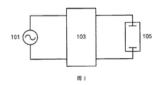
- FIG. 1 schematically shows a simplified diagram of a plasma generating apparatus in accordance with an embodiment of the present disclosure
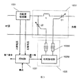
- FIG. 2 schematically shows a block diagram of a plasma generating apparatus according to an embodiment of the present disclosure
- FIG. 3 schematically shows a simplified circuit diagram of an impedance matching device in accordance with an embodiment of the present disclosure
- FIG. 4 schematically illustrates an operational timing diagram in accordance with an embodiment of the present disclosure
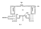
- FIG. 5 schematically illustrates a simplified cross-sectional view of a plasma etch machine in accordance with an embodiment of the present disclosure.
- FIG. 1 schematically shows a simplified diagram of a plasma generating apparatus in accordance with an embodiment of the present disclosure.
- the plasma generating apparatus includes a radio frequency (RF) source 101 and a load 105 connected to the RF source 101.
- the load 105 may include a plasma generating chamber.
- the RF source 101 is used to provide a certain RF power to excite a variable electric field in the plasma generating chamber.
- a certain degree of vacuum can be maintained in the plasma generating chamber, and the reaction gas introduced therein can be ionized under the action of a variable electric field to generate a plasma.
- the plasma generating chamber can operate based on a variety of mechanisms, such as inductively coupled plasma (ICP), capacitively coupled plasma (CCP), microwave plasma, electron cyclotron resonance (ECR) plasma, and the like.
- ICP inductively coupled plasma
- CCP capacitively coupled plasma
- ECR electron cyclotron resonance
- the output impedance of the RF source 101 is typically 50 ohms, while the input impedance of the plasma generating cavity as its load is typically a non-50 ohm impedance value having a real impedance and an imaginary impedance.
- an impedance matching device 103 is coupled between the RF source 101 and the plasma generating chamber as a load to match the impedance of the RF source 101 and the plasma generating chamber. The configuration of the impedance matching device 103 will be described in further detail below.
- FIG. 2 schematically shows a block diagram of a plasma generating apparatus in accordance with an embodiment of the present disclosure.
- the plasma generating apparatus shown in FIG. 2 also includes an RF source 101, a load (eg, a plasma generating chamber) 105, and an impedance connected between the RF source and the load.
- Matching device 103 Similar to the plasma generating apparatus described above in connection with FIG. 1, the plasma generating apparatus shown in FIG. 2 also includes an RF source 101, a load (eg, a plasma generating chamber) 105, and an impedance connected between the RF source and the load.
- Matching device 103 Similar to the plasma generating apparatus described above in connection with FIG. 1, the plasma generating apparatus shown in FIG. 2 also includes an RF source 101, a load (eg, a plasma generating chamber) 105, and an impedance connected between the RF source and the load.
- Matching device 103 Similar to the plasma generating apparatus described above in connection with FIG. 1, the plasma generating apparatus shown in FIG. 2 also includes an RF source 101, a load (eg, a plasma generating chamber) 105, and an im
- the impedance matching device 103 is for matching the impedance between the RF source 101 and the load 105 to which the RF source 101 is connected.
- the impedance matching device 103 includes:
- a motor 1035 for driving the matched impedance network 1033 to provide a certain impedance
- the controller selectively issues a first command or a second command in response to the received operating mode of the RF source 101, wherein the first command instructs the motor 1035 to drive the impedance matching network 1033 to provide a certain impedance; the second command indication
- the motor 1035 stops driving and the RF source 101 performs a frequency sweep operation.
- the RF source 101 can operate in a pulse level-level mode.
- RF source 101 can generate RF signals of a certain frequency (eg, 2 MHz, 13.56 MHz, or 60 MHz, preferably 13.56 MHz).
- PWM Pulse Width Modulation
- the RF signal can be modulated into a pulse signal with a high level and a low level in one cycle (see (a) in Figure 4). section). This pulse signal helps the plasma to ignite.
- the pulse signal can have a higher power, such as 1000 W
- the Low level phase the pulse signal can have less power (not zero), such as 600 W.
- the modulation signal may have a modulation frequency of about 10 Hz to 20 kHz, and the duty cycle (eg, the ratio of the High Level phase in one cycle) may be about 10% to 90%.
- the RF source 101 can output a PWM modulated RF signal.
- the automatic matching step or the sweep matching step can be selectively performed according to the operation mode of the RF source 101.
- the operating mode of the RF source 101 is the above-described pulse level-level mode
- in the High level phase an automatic matching step is performed.
- In the Low level phase a sweep matching step is performed.
- the working mode of the RF source 101 can be controlled by outputting the working mode information MODE, for example, instructing the RF source 101 to perform a High level phase or a Low level phase.
- the operational mode information can be output, for example, by a control unit that controls PWM modulation of the RF signal.
- the sweep matching step can also be performed in the High level phase.
- an automatic matching step is performed in the Low level phase.
- the impedance matching device 103 may include an impedance matching degree detector 1031, an impedance matching network 1033, a motor 1035, and a controller 1037.
- the impedance matching degree detector 1031 can detect the degree of impedance matching between the RF source 101 and the load 105. In theory, when the impedance between the RF source 101 and the load 105 matches, the RF power from the RF source 101 will all be transmitted to the load 105 without the reflected power from the load 105. Thus, in one example, impedance matching detection can be performed by detecting the incident voltage from RF source 101 and the reflected voltage from load 105 and comparing the two (eg, by calculating a standing wave ratio (SWR)). Of course, the present disclosure is not limited thereto, and the impedance matching degree can be detected by other various suitable means. In addition, the impedance matching degree detector 1031 may detect only relevant parameters for deriving the impedance matching degree, and send these parameters to the controller 1037 to determine the impedance matching degree by the controller 1037 without being determined by itself.
- SWR standing wave ratio
- An impedance matching network 1033 is coupled between the RF source 101 and the load 105 to provide a variable impedance and thus match the impedance between the RF source 101 and the load 105.
- the impedance matching network 1033 can include a network of impedance elements (eg, capacitive impedance elements, resistant impedance elements, etc.) connected. At least a portion of these impedance elements can have a variable impedance configuration such that the impedance matching network 1033 can present different impedance values as a whole.
- the impedance matching network 1033 can include a variable capacitance element.
- the variable capacitance element may include a rotatable member (eg, a dielectric layer between its plates or plates) that is rotated by the rotatable member to change its capacitance value.
- the motor 1035 can drive an impedance matching network 1033 (specifically, a variable impedance element such as a variable capacitance element) to provide a certain impedance value.
- a variable impedance element such as a variable capacitance element
- the motor 1035 can drive a rotatable member in the variable capacitance element to rotate, thereby changing the capacitance value of the variable capacitance element.
- Motor 1035 can be, for example, a stepper motor.
- the controller 1037 can control the overall operation of the impedance matching device 103. According to an embodiment of the present disclosure, the controller 1037 may selectively issue a first command CMD1 for the motor 1035 or a second command CMD2 for the RF source 101 according to an operation mode of the RF source 101.
- the first command CMD1 may instruct the motor 1035 to drive the impedance matching network 1035 to achieve a certain impedance.
- Driving information eg, direction of rotation, angle of rotation, etc.
- the controller 1037 may receive the impedance matching degree detected by the impedance matching degree detector 1031 (for example, represented by SWR) or derive the impedance matching degree according to the parameter detected by the impedance matching degree detector 1031, and match the impedance according to the impedance.
- the drive information of the motor 1035 is obtained.
- the motor 1035 can accordingly rotate (eg, advance or retreat) a certain angle based on the received drive information to change (eg, increase or decrease) the impedance value provided by the impedance matching network 1033.
- controller 1037 can implement control such that SWR changes toward a direction close to 1 until SWR is as close as possible or even equal to 1 (meaning the impedance is perfectly matched).
- the second command CMD2 may instruct the RF source 101 to perform a frequency sweep operation.
- the RF signal generator in the RF source 101 can change the frequency of the RF signal it generates within a certain range (eg, from 12.88 MHz to 14.32 MHz) according to the received second command CMD2.
- the impedance of the impedance matching network 1033 also changes (eg, the impedance of the capacitor and inductor changes with the signal frequency).
- controller 1037 can implement control such that SWR changes toward a direction close to 1 such that SWR is as close as possible to or equal to one.
- the motor drive impedance matching operation and the sweep impedance matching operation can be performed alternatively.
- the controller 1037 may issue the first command CMD1; in the Low level phase, the controller 1037 may issue the second command CMD2. That is, in the High level phase, the impedance matching network 1033 can be driven by the motor 1035 to provide impedance matching (in which case the scanning operation can be stopped), and in the Low level phase, the impedance matching can be provided by the sweep operation of the RF source 101. (At this point, the motor can stop driving, for example, at the end of the last drive).
- the controller 1037 may issue the first command CMD1, and in the High level phase, the controller 1037 may issue the second command CMD2. That is, in the Low level phase, the impedance matching network 1033 can be driven by the motor 1035 to provide impedance matching (in which case the scanning operation can be stopped), and in the High level phase, the impedance matching can be provided by the sweep operation of the RF source 101. (At this point, the motor can stop driving, for example, at the end of the last drive).
- FIG. 3 schematically shows a simplified circuit diagram of an impedance matching device in accordance with an embodiment of the present disclosure.
- an impedance matching network 1033 consisting of an inductive element L and variable capacitance elements C1 and C2 is shown.
- the variable capacitance elements C1 and C2 are series capacitors and parallel capacitors, respectively, to provide different impedance components.
- the impedance matching degree detector 1031 can detect the incident voltage and the reflected voltage, and transmit the detected incident voltage and reflected voltage to the controller 1037.
- the controller 1037 can calculate the impedance matching degree (for example, expressed in SWR) based on the received incident voltage and reflected voltage.
- the motor 1035 can include a motor driver 1035D and a pivot shaft 1035S.
- a motor driver 1035D corresponding to the two variable capacitance elements C1 and C2, two pivot shafts 1035S may be provided for rotating the rotatable members of the variable capacitance elements C1 and C2, respectively.
- the motor driver 1035D can drive the pivot shaft 1035S to rotate correspondingly based on the drive information received from the controller 1037.
- FIG. 4 schematically illustrates an operational timing diagram in accordance with an embodiment of the present disclosure.
- the RF source can operate in a pulse-level-level mode and thus have alternating high-level and low-level phases. .
- the first command CMD1 in the High level phase, may be at a high level, indicating that the motor is rotating to drive the impedance matching network to adjust the impedance, and the second command CMD2 can be low, indicating that the RF source is off the sweep operation.
- the first command CMD1 in the Low level phase, can be at a low level, indicating that the motor stops rotating, and the motor can remain at the end of the last High level phase, while the second command CMD can be at a high level, indicating the RF source. Turn on the sweep operation. Repeat the above cycle until the RF source stops outputting.
- the first command CMD1 in the High level phase, may be at a low level, indicating that the motor is not moving, and the second command CMD may be at a high level. Instruct the RF source to turn on the sweep operation.
- the first command CMD1 In the Low level phase, the first command CMD1 may be at a high level, indicating that the motor is rotating to drive the impedance matching network to adjust the impedance, while the second command CMD2 may be at a low level, indicating that the RF source is off the sweep operation. Repeat the above cycle until the RF source stops outputting.
- a motor-driven impedance matching network is used for impedance matching in both the High level stage and the Low level stage.
- the impedances of the High level phase and the Low level phase differ greatly, it is difficult to achieve impedance matching that satisfies the process requirements.
- the motor response speed can not keep up with the High level and Low level impedance switching speed (PWM modulation frequency)
- PWM modulation frequency the High level and Low level impedance switching speed
- a combination of motor drive impedance matching and sweep impedance matching is employed.
- the automatic matching step or the frequency sweep matching step is selectively performed according to the operating mode of the radio frequency source. Therefore, the unstable and non-repetitive phenomenon caused by the impedance change too fast in the impedance matching process can be effectively avoided, and a large process window and process stability can be realized.
- the present invention further provides an impedance matching method for matching impedance between a load connected to a radio frequency source and a radio frequency source, and the impedance matching method includes:
- the motor is instructed to drive a matching impedance network to provide a certain impedance
- the motor is instructed to stop driving and the RF source is swept.
- the working mode of the radio frequency source is a pulse level-level mode
- the pulse level-level mode includes a high level stage and a low level (Low level). stage.
- the impedance matching method provided by the invention can effectively avoid the unstable and non-repetitive phenomenon caused by the impedance change too fast in the impedance matching process, and can realize a large process window and process stability.
- the sweep matching step can also be performed in the high level phase; in the low level phase, the automatic matching step is performed.
- the power output of the RF source in the high level phase is different from the power output in the low level phase.
- the pulse signal in the High level phase, may have a larger power, such as 1000 W, while in the Low level phase, the pulse signal may have a lower power (not zero), such as 600 W.
- the present invention also provides a plasma generating apparatus including a radio frequency source, a load connected to the radio frequency source, and an impedance matching device for matching an impedance between the radio frequency source and the load, the impedance
- the matching device employs the above impedance matching device provided by the present invention.
- the plasma generating apparatus provided by the present invention can realize a large process window and process stability by using the above-mentioned impedance matching device provided by the present invention, and can be applied to a high-precision plasma etching machine.
- FIG. 5 schematically illustrates a simplified cross-sectional view of a plasma etch machine in accordance with an embodiment of the present disclosure.
- the plasma etch machine can include a closed cavity 505.
- the chamber 505 is evacuated by a vacuum system to maintain a certain degree of vacuum in the chamber 505.
- a substrate stage 505W is disposed under the cavity 505, and the substrate may be disposed on the substrate stage 505W for etching.
- the substrate stage 505W can be connected to the RF source (via, for example, the impedance matching device described above provided by the present invention).
- the coil 505L can be wound.
- the coil 505L can be coupled to an RF source (which can be separated from the RF source of the substrate stage 505W) via an impedance matching device such as described above to receive RF power.
- the coil 505L can induce a variable electric field in the cavity 505.
- the reactive gas introduced through the gas system is excited by a variable electric field to generate ionization and form a plasma, including charged electrons and ions.
- the reactive group can chemically react with the surface of the material to be etched (e.g., the layer of material formed on the substrate) on the substrate placed on the substrate stage 505W, and form a volatile reaction product.
- the reaction product can be detached from the surface of the etched material and extracted by the vacuum system.
- a DC offset can be applied to the substrate stage 505W to accelerate the positively charged reactive gas ions against the surface of the etched material. This ion bombardment can greatly accelerate the chemical reaction of the surface and the desorption of the reaction product, thereby increasing the etching rate.
- ICP etching machine is described herein, the present disclosure is not limited thereto.
- the technology of the present disclosure can also be applied to other plasma etching machines such as inductively coupled plasma generating devices, capacitively coupled plasma generating devices, microwave plasma generating devices, or electron cyclotron resonance plasma generating devices, and the like.
Landscapes
- Physics & Mathematics (AREA)
- Engineering & Computer Science (AREA)
- Plasma & Fusion (AREA)
- Chemical & Material Sciences (AREA)
- Analytical Chemistry (AREA)
- Plasma Technology (AREA)
- Drying Of Semiconductors (AREA)
Abstract
Description
Claims (10)
- 一种阻抗匹配方法,用于对射频源和所述射频源连接的负载之间的阻抗进行匹配,其特征在于,所述阻抗匹配方法包括:根据所述射频源的工作模式,选择性地进行自动匹配步骤或者扫频匹配步骤;其中,在所述自动匹配步骤中,指示电机驱动匹配阻抗网络以提供一定的阻抗;在所述扫频匹配步骤中,指示电机停止驱动以及所述射频源进行扫频操作。
- 根据权利要求1所述的阻抗匹配方法,其特征在于,所述射频源的工作模式为脉冲双电平模式,所述脉冲双电平模式包括高电平阶段和低电平阶段;在所述高电平阶段,进行所述自动匹配步骤;在所述低电平阶段,进行所述扫频匹配步骤;或者,在所述高电平阶段,进行所述扫频匹配步骤;在所述低电平阶段,进行所述自动匹配步骤。
- 根据权利要求2所述的阻抗匹配方法,其特征在于,所述射频源在所述高电平阶段输出的功率与在所述低电平阶段输出的功率不同。
- 一种阻抗匹配装置,用于对射频源和所述射频源连接的负载之间的阻抗进行匹配,其特征在于,所述阻抗匹配装置包括:匹配阻抗网络;电机,用于驱动所述匹配阻抗网络以提供一定的阻抗;以及控制器,用于根据所述射频源的工作模式,选择性地发出第一指令或第 二指令,其中,所述第一指令指示所述电机驱动阻抗匹配网络以提供一定的阻抗;所述第二指令指示所述电机停止驱动以及所述射频源进行扫频操作。
- 根据权利要求4所述的阻抗匹配装置,其特征在于,所述射频源的工作模式为脉冲双电平模式,所述脉冲双电平模式包括高电平阶段和低电平阶段;在所述高电平阶段,所述控制器发出所述第一指令;在所述低电平阶段,所述控制器发出所述第二指令;或者,在所述高电平阶段,所述控制器发出所述第二指令;在所述低电平阶段,所述控制器发出所述第一指令。
- 根据权利要求4所述的阻抗匹配装置,其特征在于,所述射频源的频率为2MHz、13.56MHz、60MHz中至少之一。
- 根据权利要求5所述的阻抗匹配装置,其特征在于,所述射频源以10Hz-20kHz的调制频率、10%-90%的占空比被脉冲调制。
- 一种等离子体产生设备,包括射频源、与所述射频源连接的负载,以及用于对所述射频源和负载之间的阻抗进行匹配的阻抗匹配装置,其特征在于,所述阻抗匹配装置采用权利要求4-7任意一项所述的阻抗匹配装置。
- 根据权利要求8所述的等离子体产生设备,其特征在于,所述等离子体产生设备包括电感耦合等离子体产生设备、电容耦合等离子体产生设备、微波等离子体产生设备或者电子回旋共振等离子体产生设备。
- 根据权利要求8所述的等离子体产生设备,其特征在于,所述等离子体产生设备用于等离子体刻蚀机。
Priority Applications (4)
| Application Number | Priority Date | Filing Date | Title |
|---|---|---|---|
| JP2019569715A JP2020527822A (ja) | 2017-06-15 | 2018-05-21 | インピーダンス整合方法、インピーダンス整合器及びプラズマ生成装置 |
| US16/620,841 US10886105B2 (en) | 2017-06-15 | 2018-05-21 | Impedance matching method, impedance matching device and plasma generating apparatus |
| KR1020197029956A KR102194201B1 (ko) | 2017-06-15 | 2018-05-21 | 임피던스 매칭 방법, 임피던스 매칭 장치 및 플라즈마 생성 디바이스 |
| SG11201911896SA SG11201911896SA (en) | 2017-06-15 | 2018-05-21 | Impedance matching method, impedance matching device and plasma generating apparatus |
Applications Claiming Priority (2)
| Application Number | Priority Date | Filing Date | Title |
|---|---|---|---|
| CN201710454753.3 | 2017-06-15 | ||
| CN201710454753.3A CN109148250B (zh) | 2017-06-15 | 2017-06-15 | 阻抗匹配装置和阻抗匹配方法 |
Publications (1)
| Publication Number | Publication Date |
|---|---|
| WO2018228133A1 true WO2018228133A1 (zh) | 2018-12-20 |
Family
ID=64660035
Family Applications (1)
| Application Number | Title | Priority Date | Filing Date |
|---|---|---|---|
| PCT/CN2018/087612 Ceased WO2018228133A1 (zh) | 2017-06-15 | 2018-05-21 | 阻抗匹配方法、阻抗匹配装置及等离子体产生设备 |
Country Status (6)
| Country | Link |
|---|---|
| US (1) | US10886105B2 (zh) |
| JP (1) | JP2020527822A (zh) |
| KR (1) | KR102194201B1 (zh) |
| CN (1) | CN109148250B (zh) |
| SG (1) | SG11201911896SA (zh) |
| WO (1) | WO2018228133A1 (zh) |
Cited By (6)
| Publication number | Priority date | Publication date | Assignee | Title |
|---|---|---|---|---|
| CN111801766A (zh) * | 2019-02-07 | 2020-10-20 | Mks韩国株式会社 | 脉冲式可变频率rf发生器的驱动频率的控制方法 |
| US11984298B2 (en) | 2019-12-02 | 2024-05-14 | Lam Research Corporation | Impedance transformation in radio-frequency-assisted plasma generation |
| US11994542B2 (en) | 2020-03-27 | 2024-05-28 | Lam Research Corporation | RF signal parameter measurement in an integrated circuit fabrication chamber |
| US12136938B2 (en) | 2019-05-07 | 2024-11-05 | Lam Research Corporation | Closed-loop multiple-output radio frequency (RF) matching |
| US12205796B2 (en) | 2019-07-31 | 2025-01-21 | Lam Research Corporation | Radio frequency power generator having multiple output ports |
| US12283462B2 (en) | 2020-06-12 | 2025-04-22 | Lam Research Corporation | Control of plasma formation by RF coupling structures |
Families Citing this family (22)
| Publication number | Priority date | Publication date | Assignee | Title |
|---|---|---|---|---|
| KR102003942B1 (ko) * | 2017-11-07 | 2019-07-25 | 한국원자력연구원 | 정합 장치를 포함하는 플라즈마 발생 장치 및 임피던스 정합 방법 |
| CN110416047B (zh) * | 2018-04-27 | 2021-03-02 | 北京北方华创微电子装备有限公司 | 射频阻抗匹配的方法及装置、半导体处理设备 |
| CN118315254A (zh) * | 2019-01-22 | 2024-07-09 | 应用材料公司 | 用于控制脉冲电压波形的反馈回路 |
| JP7257918B2 (ja) * | 2019-08-29 | 2023-04-14 | 東京エレクトロン株式会社 | プラズマ処理システムおよびプラズマ着火支援方法 |
| CN110536534B (zh) * | 2019-09-06 | 2024-03-26 | 深圳市恒运昌真空技术股份有限公司 | 一种匹配箱的阻抗调节方法、装置及射频电源系统 |
| KR102889018B1 (ko) * | 2020-05-07 | 2025-11-21 | 세메스 주식회사 | 기판 처리 장치 및 기판 처리 방법 |
| CN116779407A (zh) * | 2020-10-13 | 2023-09-19 | 北京北方华创微电子装备有限公司 | 获取方法、阻抗匹配器及其方法和半导体工艺设备 |
| KR102409094B1 (ko) * | 2020-10-28 | 2022-06-15 | (주)에이에스엔지니어링 | 주파수 가변 및 복원기능을 가진 초고속 임피던스 정합 장치 및 정합 방법 |
| KR102667081B1 (ko) * | 2020-11-27 | 2024-05-17 | 세메스 주식회사 | 멀티 레벨 펄싱을 위한 장치 및 이를 포함하는 기판 처리 장치 |
| KR102478203B1 (ko) | 2021-01-19 | 2022-12-16 | (주)이큐글로벌 | 알에프 파워 전달 시스템 및 이에 있어서 파워 보정 방법 |
| KR102537241B1 (ko) * | 2021-02-18 | 2023-05-26 | (주)엘오티씨이에스 | 배기가스 처리용 유도결합 플라즈마 장치 및 이의 임피던스 매칭 방법 |
| KR102825664B1 (ko) * | 2021-12-20 | 2025-06-25 | 세메스 주식회사 | 임피던스 매칭 회로, 및 이를 포함하는 전력 공급 장치 및 플라즈마 처리 설비 |
| CN114518704B (zh) * | 2021-12-24 | 2025-04-04 | 深圳市恒运昌真空技术股份有限公司 | 射频阻抗匹配装置和方法 |
| US12301199B2 (en) | 2022-05-05 | 2025-05-13 | Applied Materials, Inc. | Impedance tuning utility of vector space defined by transmission line quantities |
| CN115020182B (zh) * | 2022-06-24 | 2025-09-12 | 北京华丞电子有限公司 | 阻抗匹配方法及匹配器 |
| DE102022118340A1 (de) * | 2022-07-21 | 2024-02-01 | TRUMPF Hüttinger GmbH + Co. KG | Verfahren zum Zünden und/oder Aufrechterhalten eines Plasmas mit einem gepulsten Hochfrequenzsignal, Leistungsgenerator und Plasmaanordnung |
| US12266506B2 (en) * | 2022-09-07 | 2025-04-01 | Applied Materials, Inc. | Scanning impedance measurement in a radio frequency plasma processing chamber |
| US12136537B2 (en) * | 2022-10-10 | 2024-11-05 | Applied Materials, Inc. | Cost effective radio frequency impedance matching networks |
| TW202431902A (zh) * | 2022-10-19 | 2024-08-01 | 日商東京威力科創股份有限公司 | 電漿處理裝置及電漿處理方法 |
| KR102690334B1 (ko) * | 2023-02-10 | 2024-08-05 | (주)에이에스이 | 플라즈마 생성 디바이스 |
| CN118588525A (zh) * | 2023-03-03 | 2024-09-03 | 北京北方华创微电子装备有限公司 | 阻抗匹配方法、等离子体设备、电子设备及存储介质 |
| CN119582792B (zh) * | 2024-11-18 | 2026-01-09 | 中国原子能科学研究院 | 一种脉冲高频电离装置的脉宽内阻抗匹配方法 |
Citations (3)
| Publication number | Priority date | Publication date | Assignee | Title |
|---|---|---|---|---|
| CN1520245A (zh) * | 2002-12-31 | 2004-08-11 | ��ķ�о�����˾ | 等离子体处理器装置和方法,以及天线 |
| CN103730316A (zh) * | 2012-10-16 | 2014-04-16 | 中微半导体设备(上海)有限公司 | 一种等离子处理方法及等离子处理装置 |
| US20160126069A1 (en) * | 2014-10-29 | 2016-05-05 | Samsung Electronics Co., Ltd. | Pulse plasma apparatus and drive method thereof |
Family Cites Families (26)
| Publication number | Priority date | Publication date | Assignee | Title |
|---|---|---|---|---|
| JP3629705B2 (ja) * | 1997-06-06 | 2005-03-16 | 東京エレクトロン株式会社 | プラズマ処理装置 |
| TW469534B (en) * | 1999-02-23 | 2001-12-21 | Matsushita Electric Industrial Co Ltd | Plasma processing method and apparatus |
| KR101137692B1 (ko) * | 2005-02-22 | 2012-04-25 | 주성엔지니어링(주) | 플라즈마 발생장치 및 이를 이용하는 플라즈마 점화방법 |
| US7312148B2 (en) * | 2005-08-08 | 2007-12-25 | Applied Materials, Inc. | Copper barrier reflow process employing high speed optical annealing |
| JP5491648B2 (ja) * | 2006-10-06 | 2014-05-14 | 東京エレクトロン株式会社 | プラズマエッチング装置およびプラズマエッチング方法 |
| JP5319150B2 (ja) * | 2008-03-31 | 2013-10-16 | 東京エレクトロン株式会社 | プラズマ処理装置及びプラズマ処理方法及びコンピュータ読み取り可能な記憶媒体 |
| KR101528528B1 (ko) * | 2008-05-14 | 2015-06-12 | 어플라이드 머티어리얼스, 인코포레이티드 | Rf 전력 전달을 위한 시간 분해된 조정 방식을 이용하는 펄스화된 플라즈마 처리를 위한 방법 및 장치 |
| GB0823565D0 (en) * | 2008-12-24 | 2009-01-28 | Oxford Instr Plasma Technology | Signal generating system |
| JP2011064173A (ja) * | 2009-09-18 | 2011-03-31 | Mitsui Eng & Shipbuild Co Ltd | 高電圧プラズマ発生装置 |
| US8723423B2 (en) * | 2011-01-25 | 2014-05-13 | Advanced Energy Industries, Inc. | Electrostatic remote plasma source |
| JP5867701B2 (ja) * | 2011-12-15 | 2016-02-24 | 東京エレクトロン株式会社 | プラズマ処理装置 |
| US9368329B2 (en) * | 2012-02-22 | 2016-06-14 | Lam Research Corporation | Methods and apparatus for synchronizing RF pulses in a plasma processing system |
| US9530620B2 (en) * | 2013-03-15 | 2016-12-27 | Lam Research Corporation | Dual control modes |
| JP6312405B2 (ja) * | 2013-11-05 | 2018-04-18 | 東京エレクトロン株式会社 | プラズマ処理装置 |
| US9318304B2 (en) * | 2013-11-11 | 2016-04-19 | Applied Materials, Inc. | Frequency tuning for dual level radio frequency (RF) pulsing |
| US9591739B2 (en) * | 2014-05-02 | 2017-03-07 | Reno Technologies, Inc. | Multi-stage heterodyne control circuit |
| CN105826154B (zh) * | 2015-01-06 | 2017-12-19 | 北京北方华创微电子装备有限公司 | 针对脉冲射频电源的阻抗匹配方法及装置 |
| US9788405B2 (en) * | 2015-10-03 | 2017-10-10 | Applied Materials, Inc. | RF power delivery with approximated saw tooth wave pulsing |
| US10424467B2 (en) * | 2017-03-13 | 2019-09-24 | Applied Materials, Inc. | Smart RF pulsing tuning using variable frequency generators |
| US10546724B2 (en) * | 2017-05-10 | 2020-01-28 | Mks Instruments, Inc. | Pulsed, bidirectional radio frequency source/load |
| CN115662868A (zh) * | 2017-07-07 | 2023-01-31 | 先进能源工业公司 | 等离子体功率输送系统的周期间控制系统及其操作方法 |
| US10679825B2 (en) * | 2017-11-15 | 2020-06-09 | Lam Research Corporation | Systems and methods for applying frequency and match tuning in a non-overlapping manner for processing substrate |
| WO2019099870A1 (en) * | 2017-11-17 | 2019-05-23 | Advanced Energy Industries, Inc. | Synchronized pulsing of plasma processing source and substrate bias |
| US10269540B1 (en) * | 2018-01-25 | 2019-04-23 | Advanced Energy Industries, Inc. | Impedance matching system and method of operating the same |
| US10224183B1 (en) * | 2018-03-21 | 2019-03-05 | Lam Research Corporation | Multi-level parameter and frequency pulsing with a low angular spread |
| US10304660B1 (en) * | 2018-03-21 | 2019-05-28 | Lam Research Corporation | Multi-level pulsing of DC and RF signals |
-
2017
- 2017-06-15 CN CN201710454753.3A patent/CN109148250B/zh active Active
-
2018
- 2018-05-21 WO PCT/CN2018/087612 patent/WO2018228133A1/zh not_active Ceased
- 2018-05-21 KR KR1020197029956A patent/KR102194201B1/ko active Active
- 2018-05-21 US US16/620,841 patent/US10886105B2/en active Active
- 2018-05-21 SG SG11201911896SA patent/SG11201911896SA/en unknown
- 2018-05-21 JP JP2019569715A patent/JP2020527822A/ja active Pending
Patent Citations (3)
| Publication number | Priority date | Publication date | Assignee | Title |
|---|---|---|---|---|
| CN1520245A (zh) * | 2002-12-31 | 2004-08-11 | ��ķ�о�����˾ | 等离子体处理器装置和方法,以及天线 |
| CN103730316A (zh) * | 2012-10-16 | 2014-04-16 | 中微半导体设备(上海)有限公司 | 一种等离子处理方法及等离子处理装置 |
| US20160126069A1 (en) * | 2014-10-29 | 2016-05-05 | Samsung Electronics Co., Ltd. | Pulse plasma apparatus and drive method thereof |
Cited By (8)
| Publication number | Priority date | Publication date | Assignee | Title |
|---|---|---|---|---|
| CN111801766A (zh) * | 2019-02-07 | 2020-10-20 | Mks韩国株式会社 | 脉冲式可变频率rf发生器的驱动频率的控制方法 |
| CN111801766B (zh) * | 2019-02-07 | 2023-08-25 | Mks韩国株式会社 | 脉冲式可变频率rf发生器的驱动频率的控制方法 |
| US12136938B2 (en) | 2019-05-07 | 2024-11-05 | Lam Research Corporation | Closed-loop multiple-output radio frequency (RF) matching |
| US12205796B2 (en) | 2019-07-31 | 2025-01-21 | Lam Research Corporation | Radio frequency power generator having multiple output ports |
| US11984298B2 (en) | 2019-12-02 | 2024-05-14 | Lam Research Corporation | Impedance transformation in radio-frequency-assisted plasma generation |
| US12394601B2 (en) | 2019-12-02 | 2025-08-19 | Lam Research Corporation | Impedance transformation in radio-frequency-assisted plasma generation |
| US11994542B2 (en) | 2020-03-27 | 2024-05-28 | Lam Research Corporation | RF signal parameter measurement in an integrated circuit fabrication chamber |
| US12283462B2 (en) | 2020-06-12 | 2025-04-22 | Lam Research Corporation | Control of plasma formation by RF coupling structures |
Also Published As
| Publication number | Publication date |
|---|---|
| US10886105B2 (en) | 2021-01-05 |
| CN109148250A (zh) | 2019-01-04 |
| US20200126762A1 (en) | 2020-04-23 |
| CN109148250B (zh) | 2020-07-17 |
| KR20190126387A (ko) | 2019-11-11 |
| KR102194201B1 (ko) | 2020-12-22 |
| SG11201911896SA (en) | 2020-01-30 |
| JP2020527822A (ja) | 2020-09-10 |
Similar Documents
| Publication | Publication Date | Title |
|---|---|---|
| WO2018228133A1 (zh) | 阻抗匹配方法、阻抗匹配装置及等离子体产生设备 | |
| TWI614807B (zh) | 電漿處理裝置 | |
| KR102195550B1 (ko) | 플라즈마 처리 장치 | |
| KR101902427B1 (ko) | 펄스 라디오 주파수 전원에 대한 임피던스 정합 방법 및 장치 | |
| TWI552223B (zh) | 電漿處理裝置 | |
| TWI234418B (en) | RF plasma processing method and RF plasma processing apparatus | |
| TWI588889B (zh) | 電漿處理方法及電漿處理裝置 | |
| TWI637423B (zh) | 電漿處理裝置 | |
| TWI533765B (zh) | Impedance Matching Method of Plasma Etching System | |
| TWI552224B (zh) | Semiconductor etching apparatus and semiconductor etching method | |
| CN110504149B (zh) | 射频电源的脉冲调制系统及方法 | |
| CN103619117B (zh) | 可实现快速阻抗匹配的射频电源系统 | |
| CN100569043C (zh) | 一种射频系统的控制方法及其射频匹配器 | |
| CN105070627A (zh) | 一种减少基片材料受高能离子轰击损伤的方法 | |
| JP5094289B2 (ja) | プラズマ処理装置 | |
| KR20010076954A (ko) | 고주파 정합장치 |
Legal Events
| Date | Code | Title | Description |
|---|---|---|---|
| 121 | Ep: the epo has been informed by wipo that ep was designated in this application |
Ref document number: 18816899 Country of ref document: EP Kind code of ref document: A1 |
|
| ENP | Entry into the national phase |
Ref document number: 20197029956 Country of ref document: KR Kind code of ref document: A |
|
| ENP | Entry into the national phase |
Ref document number: 2019569715 Country of ref document: JP Kind code of ref document: A |
|
| NENP | Non-entry into the national phase |
Ref country code: DE |
|
| 122 | Ep: pct application non-entry in european phase |
Ref document number: 18816899 Country of ref document: EP Kind code of ref document: A1 |