WO2018216613A1 - 表示装置 - Google Patents
表示装置 Download PDFInfo
- Publication number
- WO2018216613A1 WO2018216613A1 PCT/JP2018/019290 JP2018019290W WO2018216613A1 WO 2018216613 A1 WO2018216613 A1 WO 2018216613A1 JP 2018019290 W JP2018019290 W JP 2018019290W WO 2018216613 A1 WO2018216613 A1 WO 2018216613A1
- Authority
- WO
- WIPO (PCT)
- Prior art keywords
- hole
- panel
- chassis
- optical member
- liquid crystal
- Prior art date
- Legal status (The legal status is an assumption and is not a legal conclusion. Google has not performed a legal analysis and makes no representation as to the accuracy of the status listed.)
- Ceased
Links
Images


Classifications
-
- G—PHYSICS
- G02—OPTICS
- G02F—OPTICAL DEVICES OR ARRANGEMENTS FOR THE CONTROL OF LIGHT BY MODIFICATION OF THE OPTICAL PROPERTIES OF THE MEDIA OF THE ELEMENTS INVOLVED THEREIN; NON-LINEAR OPTICS; FREQUENCY-CHANGING OF LIGHT; OPTICAL LOGIC ELEMENTS; OPTICAL ANALOGUE/DIGITAL CONVERTERS
- G02F1/00—Devices or arrangements for the control of the intensity, colour, phase, polarisation or direction of light arriving from an independent light source, e.g. switching, gating or modulating; Non-linear optics
- G02F1/01—Devices or arrangements for the control of the intensity, colour, phase, polarisation or direction of light arriving from an independent light source, e.g. switching, gating or modulating; Non-linear optics for the control of the intensity, phase, polarisation or colour
- G02F1/13—Devices or arrangements for the control of the intensity, colour, phase, polarisation or direction of light arriving from an independent light source, e.g. switching, gating or modulating; Non-linear optics for the control of the intensity, phase, polarisation or colour based on liquid crystals, e.g. single liquid crystal display cells
- G02F1/133—Constructional arrangements; Operation of liquid crystal cells; Circuit arrangements
- G02F1/1333—Constructional arrangements; Manufacturing methods
- G02F1/133308—Support structures for LCD panels, e.g. frames or bezels
-
- G—PHYSICS
- G02—OPTICS
- G02B—OPTICAL ELEMENTS, SYSTEMS OR APPARATUS
- G02B6/00—Light guides; Structural details of arrangements comprising light guides and other optical elements, e.g. couplings
- G02B6/0001—Light guides; Structural details of arrangements comprising light guides and other optical elements, e.g. couplings specially adapted for lighting devices or systems
- G02B6/0011—Light guides; Structural details of arrangements comprising light guides and other optical elements, e.g. couplings specially adapted for lighting devices or systems the light guides being planar or of plate-like form
- G02B6/0081—Mechanical or electrical aspects of the light guide and light source in the lighting device peculiar to the adaptation to planar light guides, e.g. concerning packaging
- G02B6/0086—Positioning aspects
- G02B6/0088—Positioning aspects of the light guide or other optical sheets in the package
-
- G—PHYSICS
- G02—OPTICS
- G02F—OPTICAL DEVICES OR ARRANGEMENTS FOR THE CONTROL OF LIGHT BY MODIFICATION OF THE OPTICAL PROPERTIES OF THE MEDIA OF THE ELEMENTS INVOLVED THEREIN; NON-LINEAR OPTICS; FREQUENCY-CHANGING OF LIGHT; OPTICAL LOGIC ELEMENTS; OPTICAL ANALOGUE/DIGITAL CONVERTERS
- G02F1/00—Devices or arrangements for the control of the intensity, colour, phase, polarisation or direction of light arriving from an independent light source, e.g. switching, gating or modulating; Non-linear optics
- G02F1/01—Devices or arrangements for the control of the intensity, colour, phase, polarisation or direction of light arriving from an independent light source, e.g. switching, gating or modulating; Non-linear optics for the control of the intensity, phase, polarisation or colour
- G02F1/13—Devices or arrangements for the control of the intensity, colour, phase, polarisation or direction of light arriving from an independent light source, e.g. switching, gating or modulating; Non-linear optics for the control of the intensity, phase, polarisation or colour based on liquid crystals, e.g. single liquid crystal display cells
- G02F1/133—Constructional arrangements; Operation of liquid crystal cells; Circuit arrangements
- G02F1/1333—Constructional arrangements; Manufacturing methods
-
- G—PHYSICS
- G02—OPTICS
- G02F—OPTICAL DEVICES OR ARRANGEMENTS FOR THE CONTROL OF LIGHT BY MODIFICATION OF THE OPTICAL PROPERTIES OF THE MEDIA OF THE ELEMENTS INVOLVED THEREIN; NON-LINEAR OPTICS; FREQUENCY-CHANGING OF LIGHT; OPTICAL LOGIC ELEMENTS; OPTICAL ANALOGUE/DIGITAL CONVERTERS
- G02F1/00—Devices or arrangements for the control of the intensity, colour, phase, polarisation or direction of light arriving from an independent light source, e.g. switching, gating or modulating; Non-linear optics
- G02F1/01—Devices or arrangements for the control of the intensity, colour, phase, polarisation or direction of light arriving from an independent light source, e.g. switching, gating or modulating; Non-linear optics for the control of the intensity, phase, polarisation or colour
- G02F1/13—Devices or arrangements for the control of the intensity, colour, phase, polarisation or direction of light arriving from an independent light source, e.g. switching, gating or modulating; Non-linear optics for the control of the intensity, phase, polarisation or colour based on liquid crystals, e.g. single liquid crystal display cells
- G02F1/133—Constructional arrangements; Operation of liquid crystal cells; Circuit arrangements
- G02F1/1333—Constructional arrangements; Manufacturing methods
- G02F1/1335—Structural association of cells with optical devices, e.g. polarisers or reflectors
- G02F1/133528—Polarisers
-
- G—PHYSICS
- G02—OPTICS
- G02B—OPTICAL ELEMENTS, SYSTEMS OR APPARATUS
- G02B6/00—Light guides; Structural details of arrangements comprising light guides and other optical elements, e.g. couplings
- G02B6/0001—Light guides; Structural details of arrangements comprising light guides and other optical elements, e.g. couplings specially adapted for lighting devices or systems
- G02B6/0011—Light guides; Structural details of arrangements comprising light guides and other optical elements, e.g. couplings specially adapted for lighting devices or systems the light guides being planar or of plate-like form
- G02B6/0033—Means for improving the coupling-out of light from the light guide
- G02B6/005—Means for improving the coupling-out of light from the light guide provided by one optical element, or plurality thereof, placed on the light output side of the light guide
- G02B6/0055—Reflecting element, sheet or layer
-
- G—PHYSICS
- G02—OPTICS
- G02F—OPTICAL DEVICES OR ARRANGEMENTS FOR THE CONTROL OF LIGHT BY MODIFICATION OF THE OPTICAL PROPERTIES OF THE MEDIA OF THE ELEMENTS INVOLVED THEREIN; NON-LINEAR OPTICS; FREQUENCY-CHANGING OF LIGHT; OPTICAL LOGIC ELEMENTS; OPTICAL ANALOGUE/DIGITAL CONVERTERS
- G02F1/00—Devices or arrangements for the control of the intensity, colour, phase, polarisation or direction of light arriving from an independent light source, e.g. switching, gating or modulating; Non-linear optics
- G02F1/01—Devices or arrangements for the control of the intensity, colour, phase, polarisation or direction of light arriving from an independent light source, e.g. switching, gating or modulating; Non-linear optics for the control of the intensity, phase, polarisation or colour
- G02F1/13—Devices or arrangements for the control of the intensity, colour, phase, polarisation or direction of light arriving from an independent light source, e.g. switching, gating or modulating; Non-linear optics for the control of the intensity, phase, polarisation or colour based on liquid crystals, e.g. single liquid crystal display cells
- G02F1/133—Constructional arrangements; Operation of liquid crystal cells; Circuit arrangements
- G02F1/1333—Constructional arrangements; Manufacturing methods
- G02F1/133308—Support structures for LCD panels, e.g. frames or bezels
- G02F1/133314—Back frames
-
- G—PHYSICS
- G02—OPTICS
- G02F—OPTICAL DEVICES OR ARRANGEMENTS FOR THE CONTROL OF LIGHT BY MODIFICATION OF THE OPTICAL PROPERTIES OF THE MEDIA OF THE ELEMENTS INVOLVED THEREIN; NON-LINEAR OPTICS; FREQUENCY-CHANGING OF LIGHT; OPTICAL LOGIC ELEMENTS; OPTICAL ANALOGUE/DIGITAL CONVERTERS
- G02F2201/00—Constructional arrangements not provided for in groups G02F1/00 - G02F7/00
- G02F2201/56—Substrates having a particular shape, e.g. non-rectangular
Definitions
- the present invention relates to a display device.
- the liquid crystal display device described in Patent Document 1 is an optical member having a sheet shape for imparting an optical action to an LED and light from the LED, and a through hole is formed so as to penetrate in the thickness direction.
- a regulating portion that regulates displacement of the optical member in a direction along the plate surface by passing through the through hole and contacting the inner surface thereof, and having a communicating hole communicating with the through hole.
- a backlight device comprising:
- the liquid crystal panel is provided with a panel-side through hole communicating with the through-hole of the backlight device, and a cap member passed through the through-hole and the panel-side through hole. Is provided.
- the cap edge can protect the edge of the panel side through hole in the liquid crystal panel.
- the cap member is provided with a hook-shaped pressing portion, a portion where an image cannot be displayed tends to be wide in the vicinity of the panel side through hole.
- the present invention has been completed based on the above-described circumstances, and aims to widen the range in which an image can be displayed.
- the display device of the present invention has a panel through-hole penetrating in the thickness direction and displaying an image, a light source that emits light for display on the display panel, and a housing that houses the light source.
- the panel through-holes that penetrate the display panel along the thickness direction are arranged in such a manner that the housing through-holes that penetrate the housing that houses the light source communicate with each other. It is possible to put an external object in Since the housing through hole is smaller than the panel through hole, when an external object is put into the panel through hole and the housing through hole as described above, the object is a relatively small housing. It is easy to interfere with the hole edge of the through hole, and it is difficult to interfere with the hole edge of the relatively large panel through hole. Therefore, damage or the like hardly occurs at the edge of the panel through-hole in the display panel that is generally lower in mechanical strength than the housing.
- this is suitable when, for example, an object for positioning the display device is placed in the panel through hole and the housing through hole.
- the light in the vicinity of the housing through-hole is reduced by making the housing through-hole smaller than the panel through-hole. It is difficult for the portion that cannot be irradiated to overlap with the portion that can display an image on the display panel. As a result, display unevenness hardly occurs on the display panel, and the display quality is hardly deteriorated.
- the range in which an image can be displayed can be widened.
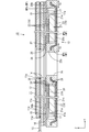
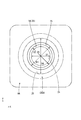
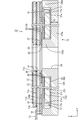
- FIG. 1 is a plan view of a liquid crystal panel provided in a liquid crystal display device according to Embodiment 1 of the present invention. Sectional drawing which cut
- FIGS. 1 A first embodiment of the present invention will be described with reference to FIGS.
- a liquid crystal display device (display device) 10 is illustrated.
- a part of each drawing shows an X axis, a Y axis, and a Z axis, and each axis direction is drawn to be a direction shown in each drawing.
- FIG. 2 is used as a reference, and the upper side of the figure is the front side and the lower side of the figure is the back side.
- the liquid crystal display device 10 has a substantially circular shape as a whole, and as shown in FIG. 1, a liquid crystal panel (display panel) 11 capable of displaying an image and front and back surfaces attached to the outer surfaces of the front and back surfaces of the liquid crystal panel 11. At least a pair of polarizing plates 12 and a backlight device (illumination device) 13 that is disposed on the back side (back side) of the liquid crystal panel 11 and supplies light for display to the liquid crystal panel 11 are provided. .
- the liquid crystal display device 10 according to the present embodiment is preferably used for a wearable terminal (not shown) such as a smart watch, but is not necessarily limited thereto.
- the liquid crystal panel 11 As shown in FIG. 1, the liquid crystal panel 11 has a substantially circular shape when viewed in plan, and a panel through hole 14 is formed through the center in the thickness direction (Z-axis direction). .
- the panel through hole 14 has a circular planar shape. Therefore, the liquid crystal panel 11 has a substantially annular shape (substantially donut shape) as a whole.
- the outer shape of the liquid crystal panel 11 has an arcuate shape (curved shape) when viewed in plan, whereas a part thereof is linear when viewed in plan.
- a pair of linear portions are arranged in parallel with each other at positions spaced by an angular interval of about 180 ° in the circumferential direction around the center of the liquid crystal panel 11.
- a flexible substrate 15 to be described later is mounted on one side.
- the extending direction of the linear portion at the outer peripheral end of the liquid crystal panel 11 is illustrated so that the X-axis direction and the direction perpendicular to the extending direction coincide with the Y-axis direction. Yes.
- the thickness direction of the liquid crystal panel 11 (the polarizing plate 12, the optical member 19, and the optical member support portion 20 a) is illustrated so as to coincide with the Z-axis direction.
- the liquid crystal panel 11 has a display area AA in which an image is displayed using light emitted from the backlight device 13, and the planar shape thereof has an annular shape. Furthermore, the liquid crystal panel 11 includes a central non-display area (central non-display area) CNAA located on the inner peripheral side of the display area AA and an outer peripheral side disposed on the outer peripheral side of the display area AA. Non-display area ONAA, and no image is displayed in the center-side non-display area CNAA and the outer peripheral-side non-display area ONAA.
- the center-side non-display area CNAA includes a hole of the panel through-hole 14 in addition to the panel through-hole 14 and has a circular shape when viewed from above.
- the liquid crystal panel 11 is similar in plan shape to the panel through hole 14 and the center-side non-display area CNAA, and thereby has an excellent appearance when an image is displayed in the display area AA.
- the outer peripheral side non-display area ONAA has a substantially annular shape when viewed in plan, and the planar shape of the inner peripheral end thereof is circular, whereas the planar shape of the outer peripheral end is identical to the outer shape of the liquid crystal panel 11. I'm doing it.
- boundary positions between the display area AA, the center-side non-display area CNAA, and the outer peripheral-side non-display area ONAA are respectively illustrated by dashed lines.
- the liquid crystal panel 11 is sandwiched between a pair of glass substrates 11a and 11b that are substantially transparent and have excellent translucency, and optical characteristics in accordance with the application of an electric field.
- a liquid crystal 11c that includes liquid crystal molecules that are substances that change, an outer peripheral side sealing portion 11d that surrounds the liquid crystal 11c and that is interposed between the outer peripheral end portions of the pair of substrates 11a and 11b, and seals the liquid crystal 11c; And at least an inner peripheral seal portion 11e that seals the liquid crystal 11c by being interposed between inner peripheral end portions of the substrates 11a and 11b.
- the outer peripheral side seal portion 11d is provided in a shape extending in a substantially annular shape along the outer shape of the liquid crystal panel 11, and is disposed in the outer peripheral side non-display area ONAA.
- the inner peripheral side seal portion 11e is provided in a shape extending in a substantially annular shape along the hole edge of the panel through-hole 14, and is disposed in the center-side non-display area CNAA.
- the front side (front side) is the CF substrate 11a
- the back side (back side) is the array substrate 11b.
- the array substrate 11b has one linear portion of the outer peripheral end portion flush with the same linear portion of the CF substrate 11a, but the other linear portion
- the CF substrate 11a is arranged so as to protrude outward from the same linear portion, and the flexible substrate 15 is attached to the protruding portion.
- a driver (not shown) is mounted on the flexible substrate 15 by COF (Chip On Film). The driver can process various input signals supplied from a panel drive circuit board (not shown) and supply the processed signals to the liquid crystal panel 11.
- the internal structure in the display area AA of the liquid crystal panel 11 (all of which are not shown) will be briefly described, but the illustration of various structures described below is omitted.
- a TFT Thin Film Transistor
- a large number of pixel electrodes are arranged in a matrix (matrix).
- a grid-like gate wiring and source wiring are disposed so as to surround them. A signal related to an image is supplied to the gate wiring and the source wiring by the driver described above.
- the pixel electrode disposed in the rectangular region surrounded by the gate wiring and the source wiring is made of a transparent electrode material.
- a large number of color filters are arranged side by side at positions corresponding to the respective pixel electrodes.
- the color filter is arranged so that three colors of R, G, and B are alternately arranged.
- a light shielding layer (black matrix) for preventing color mixture is formed between the color filters.
- a counter electrode facing the pixel electrode on the array substrate 11b side is provided on the surface of the color filter and the light shielding layer.
- An alignment film (not shown) for aligning liquid crystal molecules contained in the liquid crystal 11c is formed on the inner surfaces of both the substrates 11a and 11b.
- the liquid crystal panel 11 having the above-described configuration is fixed to the backlight device 13 by a panel fixing tape (panel fixing member) 16.
- the panel fixing tape 16 is made of a synthetic resin, and is formed by applying an adhesive material on both sides of a frame-like base material extending along the outer peripheral edge of the liquid crystal panel 11 as a whole.
- the base material of the panel fixing tape 16 has a light shielding property because the surface thereof is black, so that leakage light from the backlight device 13 is transmitted through the outer peripheral side non-display area ONAA of the liquid crystal panel 11. Is prevented.
- the backlight device 13 has a substantially circular shape when viewed from the top in the same manner as the liquid crystal panel 11 as viewed in a plan view, and as shown in FIG. On the opposite side).
- the backlight device 13 gives an optical action to the liquid crystal panel 11 by providing an LED (Light Emitting Diode) 17 that is a light source, an LED substrate (light source substrate) 18 on which the LED 17 is mounted, and light from the LED 17. And an optical member 19 for emitting the light and a chassis (housing) 20 for housing them.
- LED Light Emitting Diode
- the optical member 19 includes a light guide plate (optical member) 21 that guides light from the LEDs 17, a plurality of optical sheets (optical members) 22 that are stacked on the front side of the light guide plate 21, and a back side of the light guide plate 21. At least a reflection sheet (optical member, reflection member) 23 arranged in a stacked manner is included.
- the backlight device 13 is of an edge light type (side light type) in which LEDs 17 (LED substrates 18) are arranged at positions that overlap at least a pair of linear portions of the outer peripheral end of the liquid crystal panel 11. .
- the backlight device 13 emits light from the LED 17 toward the liquid crystal panel 11 on the front side from the opening portion of the chassis 20 while converting the light from the LED 17 into planar light by the optical action of the optical member 19. That is, the front side with respect to the backlight device 13 is the light output side.
- the components of the backlight device 13 will be described sequentially.
- the LED 17 has a configuration in which an LED chip (LED element), which is a semiconductor light emitting element, is sealed with a resin material on a substrate portion fixed to the plate surface of the LED substrate 18.
- the LED chip mounted on the substrate unit has one main emission wavelength, and specifically, one that emits blue light in a single color is used.
- the resin material that seals the LED chip is dispersed and blended with a phosphor that emits a predetermined color when excited by the blue light emitted from the LED chip, and generally emits white light as a whole. It is said.
- the LED 17 is a so-called side-emitting type in which a side surface adjacent to the mounting surface with respect to the LED substrate 18 is a light emitting surface 17a.
- the LED substrate 18 is made of an insulating material and has a flexible film-like (sheet-like) substrate portion (base material), and the plate surface thereof is the liquid crystal panel 11 and the optical member. It is parallel to each of the 19 plate surfaces.
- the LED 17 described above is surface-mounted on the back surface of the LED substrate 18 (the surface facing the light guide plate 21 side), and a wiring pattern (not shown) for supplying power to the LED 17 is patterned. ing.
- the LED substrate 18 is arranged so that a part thereof overlaps the front side with respect to a part of the outer peripheral end of the light guide plate 21.
- the LED substrate 18 is disposed on the back side with respect to the liquid crystal panel 11 and is fixed to the liquid crystal panel 11 with a panel fixing tape 16.
- the optical member 19 has a substantially circular shape when viewed from the top in the same manner as the liquid crystal panel 11, and is disposed at a position directly below the liquid crystal panel 11 as shown in FIG. 11 are arranged in parallel with the plate surface.
- the light guide plate 21 constituting the optical member 19 has a light incident surface (light source) on which the end surfaces of at least a pair of linear portions of the outer peripheral end portions are arranged so as to face the LEDs 17 and the light from the LEDs 17 enters. Opposing end face) 21a.
- the plate surface facing the front side is a light emitting surface 21 b that emits light toward the liquid crystal panel 11.
- the plate surface facing the back side of the light guide plate 21 is an opposite plate surface 21c opposite to the light emitting surface 21b.
- the light guide plate 21 introduces light emitted from the LED 17 in a direction substantially along the plate surface of the optical member 19 from the light incident surface 21a, and propagates the light therein while transmitting the light inside (front side, light
- the light emitting surface 21b has a function of being raised so as to face toward the emission side and emitting from the light emission surface 21b. Note that a light reflection pattern (a light reflection pattern (for reflecting light from the light emission surface 21b) is reflected on the opposite surface 21c of the light guide plate 21 to reflect the light in the light guide plate 21 toward the light emission surface 21b. (Not shown) is formed.
- the optical sheet 22 constituting the optical member 19 is placed on the front side of the light emitting surface 21 b of the light guide plate 21 and is interposed between the liquid crystal panel 11 and the light guide plate 21.
- the optical sheet 22 is provided in a form in which a plurality of sheets (three sheets in this embodiment) overlap each other, and specific types thereof include, for example, a diffusion sheet, a lens sheet (prism sheet), a reflective polarizing sheet, and the like. It can be used by appropriately selecting from these.
- the rear surface of the panel fixing tape 16 is fixed to the outer peripheral end of the optical sheet 22 arranged on the most front side.
- the reflection sheet 23 constituting the optical member 19 is arranged so as to cover the back side of the light guide plate 21, that is, the opposite plate surface 21 c opposite to the light emitting surface 21 b. Since the reflection sheet 23 is made of a synthetic resin sheet material having a silver surface with excellent light reflectivity, the reflection sheet 23 propagates through the light guide plate 21 and emits light emitted from the opposite plate surface 21c on the front side ( It can be efficiently launched toward the light exit surface 21b). The reflection sheet 23 is disposed so as to be sandwiched between the light guide plate 21 and an optical member support portion 20a of the chassis 20 described later.
- the outer peripheral end portion of the reflection sheet 23 extends outward from the outer peripheral end surface of the light guide plate 21, and particularly the end portion on the LED substrate 18 side reaches a position beyond the LED 17 from the light incident surface 21 a of the light guide plate 21. Therefore, the light from the LED 17 can be efficiently reflected by the extended portion and incident on the light incident surface 21a.
- the chassis 20 has a substantially circular shape when viewed from the top in the same manner as the liquid crystal panel 11. As shown in FIG. 2, the chassis 20 has a substantially box shape that opens toward the front as a whole.
- the LED 17, the LED substrate 18, the optical member 19, and the like can be accommodated.
- the chassis 20 includes an optical member support portion (bottom portion) 20a that supports the optical member 19 from the back side (the side opposite to the liquid crystal panel 11 side), and a frame-shaped portion that rises from the outer peripheral end of the optical member support portion 20a toward the front side. (Side part, frame-like part) 20b.
- the optical member support portion 20a has its plate surface parallel to the respective plate surfaces of the liquid crystal panel 11 and the optical member 19, and constitutes the optical member 19 accommodated in the chassis 20, and is arranged in a stacked manner. 21, the optical sheet 22 and the reflective sheet 23 are supported from the back side.
- the frame-like portion 20b is arranged so as to surround the LED 17, LED board 18, optical member 19 and the like housed in the chassis 20 from the outer peripheral side, so that the overall planar shape is a frame shape (frame shape). ). Further, the rear surface of the panel fixing tape 16 is fixed to the rising tip of the frame-shaped portion 20b.
- the chassis 20 As shown in FIGS. 2 and 3, the chassis 20 according to the present embodiment is arranged so as to penetrate the panel 20 and communicate with the panel through hole 14, and is smaller than the panel through hole 14. Hole) 24.
- the chassis through hole 24 is indicated by a two-dot chain line that is slightly smaller than the panel through hole 14.
- the chassis through hole 24 has a circular planar shape and is arranged at a position concentric with the panel through hole 14, and its diameter D1 is the diameter of the panel through hole 14. It is made smaller than the dimension D2.
- the entire area of the chassis through-hole 24 is in communication with the panel through-hole 14, and the peripheral surface of the chassis through-hole 24 is located inside the peripheral surface of the panel through-hole 14 over the entire circumference (the center of each through-hole 14, 24. Project to the side).
- the panel through holes 14 that penetrate the liquid crystal panel 11 in the thickness direction are arranged so that the chassis through holes 24 that penetrate the chassis 20 that accommodates the LEDs 17 and the like communicate with each other.
- an external object (not shown) can be put into the chassis through hole 24 from the front side or the back side.
- the external object is accommodated in a shaft part of an analog needle (long hand, short hand, second hand, etc.) or a smart watch case, for example.
- a positioning projection for positioning the liquid crystal display device 10 is used.
- the chassis through-hole 24 has a diameter D1 smaller than the diameter D2 of the panel through-hole 14, so that the panel through-holes 14 communicate with each other as described above.
- the object easily interferes with the edge of the chassis through hole 24 having a relatively small diameter D1, and the panel through hole 14 having a relatively large diameter D2. It is difficult to interfere with the hole edge. Therefore, it is less likely to be damaged due to object interference at the hole of the panel through hole 14 in the liquid crystal panel 11 made of glass and having a mechanical strength lower than that of the chassis 20.
- an external object put in the panel through hole 14 and the chassis through hole 24 is a positioning convex portion that exerts a positioning function by contacting the edge of the chassis through hole 24.
- the chassis through hole 24 penetrates the panel.
- the polarizing plate 12 arranged on the outer surface of the liquid crystal panel 11 has a polarizing plate through-hole 25 that penetrates itself in the thickness direction, as shown in FIGS.
- the polarizing plate through hole 25 is disposed in communication with the panel through hole 14 and the chassis through hole 24.
- the polarizing plate through hole 25 has a circular planar shape and is arranged at a position that is concentric with the panel through hole 14 and the chassis through hole 24.
- the diameter D3 is larger than the diameter D2 of the panel through hole 14.
- the peripheral surface of the polarizing plate through-hole 25 is recessed outside the peripheral surface of the panel through-hole 14 (on the opposite side to the center side of each through-hole 14, 24, 25) over the entire periphery.
- An optical member through hole 26 communicating with the polarizing plate through hole 25 is provided.
- the optical member through hole 26 is indicated by a two-dot chain line that is slightly larger than the polarizing plate through hole 25.
- the optical member through-hole 26 has a circular planar shape like the panel through-hole 14, chassis through-hole 24, and polarizing plate through-hole 25, and the panel through-hole 14, chassis through-hole 24, and polarizing plate through-hole.
- the diameter D4 of the chassis is larger than the diameter D1 of the chassis through hole 24. Therefore, the peripheral surface of the optical member through-hole 26 is recessed outside the peripheral surface of the chassis through-hole 24 over the entire circumference (the side opposite to the center side of each through-hole 14, 24, 25, 26).
- the chassis 20 has a cylindrical portion 20c that is arranged so as to protrude from the optical member support portion 20a toward the front side (the liquid crystal panel 11 side) and is connected to the optical member support portion 20a.
- the cylindrical portion 20 c forms a hole edge of the chassis through hole 24, and an inner peripheral surface thereof forms a peripheral surface of the chassis through hole 24.
- the cylindrical portion 20c has a cylindrical shape that is concentrically arranged with each of the through holes 14, 24, 25, and 26, and the inner diameter dimension thereof coincides with the diameter dimension D1 of the chassis through hole 24. .
- the outer diameter of the cylindrical portion 20c is larger than the diameters D1 to D3 of the panel through hole 14, the chassis through hole 24, and the polarizing plate through hole 25, but the diameter of the optical member through hole 26 of the optical member 19 is larger. It is made smaller than D4. Accordingly, when the optical member 19 is accommodated in the chassis 20, the cylindrical portion 20 c can be passed through the optical member through hole 26 of the optical member 19. As described above, the cylindrical portion 20c constituting the chassis 20 constitutes the hole edge of the chassis through-hole 24 and is arranged so as to protrude from the optical member support portion 20a toward the liquid crystal panel 11 side. When an external object is put in the through hole 24, the object can be firmly received by the cylindrical portion 20c.
- the external object put in the chassis through hole 24 is a positioning convex portion that exhibits a positioning function by contacting the cylindrical portion 20c.
- the cylindrical portion 20 c penetrates the optical member 19 in the thickness direction, communicates with the chassis through hole 24, and passes through the optical member through hole 26 larger than the chassis through hole 24. Accordingly, since the cylindrical portion 20c is arranged inside the hole edge of the optical member through hole 26 in the optical member 19, even when an external object is put in the chassis through hole 24, the object passes through the optical member. Interfering with the hole edge of the hole 26 is avoided. That is, since the optical member 19 can be protected by the cylindrical portion 20c, the optical performance of the optical member 19 can be appropriately exhibited.
- the optical member support portion 20a is made of a metal plate (sheet metal) MP, while the frame-like portion 20b and the tubular portion 20c are mainly made of a synthetic resin material. Therefore, the optical member support portion 20a has a thickness dimension T1 smaller than the thickness dimensions T2 and T3 of the frame-shaped portion 20b and the cylindrical portion 20c. The entire area of the optical member support portion 20a is made of a metal plate MP. On the other hand, the frame-like portion 20b and the cylindrical portion 20c are partly made of the metal plate material MP extended from the optical member support portion 20a, but most of the portion covering the portion made of the metal plate material MP is made of a synthetic resin material.
- the portion constituting the optical member support portion 20a is a flat plate portion MPa having a plate surface parallel to the plate surface of the optical member 19 or the like, whereas the frame-like portion 20b and the cylindrical portion A part constituting part of 20c is a bent part MPb that is bent so as to rise from the optical member supporting part 20a toward the front side.
- the portion made of the synthetic resin material is arranged so as to surround the entire region so that the bent portion MPb of the metal plate material MP is not exposed to the outside.
- an insert molding method is used.
- a flat metal plate material before molding is subjected to press molding or the like, so that a flat plate portion MPa (entire area of the optical member support portion 20a). And a bent part MPb (a part of each of the frame-like part 20b and the cylindrical part 20c) are formed.
- the processed metal plate MP is inserted into a molding die for resin molding, a synthetic resin material in a molten state is injected into the molding die, and the synthetic resin material is cooled and solidified to form a frame shape.
- the part 20b and the cylindrical part 20c are formed.
- the frame-like portion 20b and the cylindrical portion 20c can be formed by resin molding using a molding die when the chassis 20 is manufactured, the frame-like portion 20b and the chassis through-hole 24 are formed. Such dimensional accuracy and positional accuracy are high. Accordingly, the outer shape of the chassis 20 becomes appropriate, and an external object can be easily put into the chassis through hole 24. And since the optical member support part 20a of the chassis 20 consists of metal plate material MP, compared with the case where an optical member support part consists of a synthetic resin material, the optical member support part 20a becomes thin. This is suitable for reducing the thickness of the chassis 20 and the liquid crystal display device 10.
- a fixing tape (fixing member) 27 having a light shielding property is provided so as to be interposed between the liquid crystal panel 11 and the backlight device 13. ing.
- the fixing tape 27 is formed by applying an adhesive material to both surfaces of a base material made of synthetic resin.
- the fixing tape 27 has an annular shape surrounding the panel through hole 14, the chassis through hole 24, and the polarizing plate through hole 25.
- the fixing tape 27 penetrates itself in the thickness direction at the center position of the fixing tape 27 and the chassis through hole 14.
- a fixed tape through hole (fixed member through hole) 28 arranged in communication with the polarizing plate through hole 25 and the optical member through hole 26.
- the fixed tape through hole 28 has a diameter dimension (an inner diameter dimension of the fixed tape 27) D5 larger than a diameter dimension D1 of the chassis through hole 24 and is substantially the same as the diameter dimension D2 of the panel through hole 14.
- the outer diameter of the fixing tape 27 is larger than the diameter D4 of the optical member through hole 26. Accordingly, the fixing tape 27 is adhered to the hole edge of the polarizing plate through hole 25 in the polarizing plate 12 mainly adhered to the outer surface of the back side of the liquid crystal panel 11 while the adhesive material on the front side is fixed to the fixing tape 27.
- the material straddles the cylindrical portion 20c that is the hole edge of the chassis through hole 24 in the chassis 20 and the hole edge of the optical member through hole 26 in the optical sheet 22 that is disposed on the most front side of the optical member 19. It is fixed.
- the liquid crystal panel 11 and the backlight device 13 are fixed to each other by the fixing tape 27 interposed therebetween. Since the fixing tape 27 has a light shielding property, even if light leaks from the vicinity of the chassis through hole 24 of the backlight device 13 due to the chassis 20 having the chassis through hole 24, the leaked light is fixed. It can be blocked by the tape 27, thereby suppressing light leakage to the liquid crystal panel 11 side.
- the fixing tape 27 has a fixing tape through hole 28 which is arranged in a form penetrating in the thickness direction and communicating with the chassis through hole 24 and is larger than the chassis through hole 24, an external object is the chassis through hole 24.
- the hole edge of the fixing tape through-hole 28 is difficult to interfere with the object when it is put into the object.
- the liquid crystal display device (display device) 10 has the panel through hole 14 penetrating in the thickness direction and displays the image, and the liquid crystal panel 11.
- An LED (light source) 17 that emits light for display in the display, and a chassis (housing) 20 that accommodates the LED 17, and is arranged in such a manner as to pass through itself and communicate with the panel through hole 14.
- a chassis 20 having a smaller chassis through hole (housing through hole) 24.
- the panel through-hole 14 that penetrates the liquid crystal panel 11 in the thickness direction is arranged in such a manner that a chassis through-hole 24 that penetrates the chassis 20 that accommodates the LEDs 17 and the like communicates with the panel through-hole 14. It is possible to put an external object into the hole 24. And since the chassis through-hole 24 is made smaller than the panel through-hole 14, when an external object is put in the panel through-hole 14 and the chassis through-hole 24 as described above, the object is relatively small. It is easy to interfere with the hole edge of the chassis through hole 24, and it is difficult to interfere with the relatively large hole of the panel through hole 14.
- the polarizing plate 12 is disposed on the outer surface of the liquid crystal panel 11 and has a polarizing plate through-hole 25 larger than the panel through-hole 14, which is disposed so as to penetrate the thickness direction and communicate with the panel through-hole 14.
- a plate 12 is provided.
- the polarizing plate through hole 25 that penetrates the polarizing plate 12 disposed on the outer surface of the liquid crystal panel 11 in the thickness direction communicates with the panel through hole 14 and the chassis through hole 24.
- the optical member 19 is accommodated in the chassis 20 and applies an optical action to the light from the LED 17, and penetrates in the thickness direction and communicates with the chassis through hole 24 and is larger than the chassis through hole 24.
- the chassis 20 includes an optical member support portion 20a that supports the optical member 19 from the side opposite to the liquid crystal panel 11 side, and a hole edge of the chassis through hole 24 to form the optical member support portion. And at least a cylindrical portion 20c that is arranged so as to protrude from the liquid crystal panel 11 toward the liquid crystal panel 11 and is connected to the optical member support portion 20a. In this way, the light emitted from the LED 17 is irradiated toward the liquid crystal panel 11 after being given an optical action by the optical member 19.
- the optical member 19 is supported from the side opposite to the liquid crystal panel 11 side by the optical member support portion 20a constituting the chassis 20, so that its optical performance is appropriately exhibited. Since the cylindrical part 20c which comprises the chassis 20 comprises the hole edge of the chassis through-hole 24, and is distribute
- the cylindrical portion 20c is arranged inside the hole edge of the optical member through hole 26 in the optical member 19, even when an external object is put in the chassis through hole 24, the object passes through the optical member. Interfering with the hole edge of the hole 26 is avoided. That is, the optical member 19 can be protected by the cylindrical portion 20c.
- the chassis 20 has a cylindrical portion 20c made of a synthetic resin material.
- the cylindrical portion 20c can be formed by resin molding using a mold when the chassis 20 is manufactured, so that the dimensional accuracy and position accuracy of the chassis through hole 24 are high. . Thereby, it becomes easy to put an external object into the chassis through hole 24.
- the optical member support portion 20a is made of a metal plate material MP.
- the optical member support portion 20a is thinner than when the optical member support portion is made of a synthetic resin material. This is suitable for reducing the thickness of the chassis 20 and the liquid crystal display device 10.
- the chassis 20 has a frame-like portion 20b made of a synthetic resin material that is connected to the outer end portion of the optical member support portion 20a.
- the frame-shaped portion 20b connected to the outer end portion of the optical member support portion 20a constituting the chassis 20 is made of a synthetic resin material, so that the frame-shaped portion 20b can be replaced with a mold when the chassis 20 is manufactured. It can be formed by the resin molding used. Thereby, since the dimensional accuracy and position accuracy concerning the frame-shaped part 20b become high, the external shape of the chassis 20 becomes appropriate.
- the liquid crystal panel 11 and the backlight device 13 are composed of at least an LED 17 and a chassis 20, and is arranged so as to be interposed between a backlight device (illumination device) 13 for irradiating the liquid crystal panel 11 with light for display, and the liquid crystal panel 11 and the backlight device 13.
- the fixing tape 27 Since the fixing tape 27 has a light shielding property, even if light leaks from the vicinity of the chassis through hole 24 of the backlight device 13 due to the chassis 20 having the chassis through hole 24, the leaked light is fixed. It can be blocked by the tape 27, thereby suppressing light leakage to the liquid crystal panel 11 side. Since the fixing tape 27 has a fixing tape through hole 28 which is arranged in a form penetrating in the thickness direction and communicating with the chassis through hole 24 and is larger than the chassis through hole 24, an external object is the chassis through hole 24. The hole edge of the fixing tape through-hole 28 is difficult to interfere with the object when it is put into the object.
- the entire region of the optical member support portion 120a, the frame-like portion 120b, and the cylindrical portion 120c is made of a synthetic resin material.
- the thickness dimension T4 of the optical member support part 120a is larger than the thickness dimension T1 of the optical member support part 20a of the first embodiment described above.
- the frame-shaped part 120b and the cylindrical part 120c are made of a synthetic resin material, in this respect, in addition to obtaining the same operation and effect as the above-described first embodiment, the metal plate material as in the first embodiment. Therefore, it is preferable to reduce the manufacturing cost of the chassis 120.
- Embodiment 3 of the present invention will be described with reference to FIG.
- This Embodiment 3 shows what changed the planar shape of each through-hole 214,224,225,226,228 from Embodiment 1 mentioned above.
- movement, and effect as above-mentioned Embodiment 1 is abbreviate
- the panel through-hole 214, chassis through-hole 224, polarizing plate through-hole 225, optical member through-hole 226, and fixing tape through-hole 228 according to this embodiment are square in shape as shown in FIG. . Even with such a configuration, the same operations and effects as those of the first embodiment can be obtained.
- the diameter dimension of the polarizing plate through hole is substantially the same as the diameter dimension of the panel through hole. It does not matter.
- the diameter dimension of the optical member through-hole is the largest compared to the diameter dimension of other through-holes has been shown.
- the diameter may be substantially the same as the diameter of the panel through hole.
- the diameter dimension of the fixed tape through hole is substantially the same as the diameter dimension of the panel through hole.
- the diameter dimension of the fixed tape through hole is the diameter dimension of the panel through hole.
- the diameter dimension of the fixed tape through hole may be larger than the diameter dimension of the panel through hole.
- the case where all the planar shapes of the respective through-holes are the same is shown. However, a part of each through-hole may have a different planar shape.
- the chassis may have a configuration without the cylindrical portion. In this case, the chassis through hole is provided so as to penetrate the optical member supporting portion, and the optical member supporting portion has the hole edge of the chassis through hole. It is also possible to remove the frame portion from the chassis.
- SYMBOLS 10 Liquid crystal display device (display device), 11 ... Liquid crystal panel (display panel), 12 ... Polarizing plate, 13 ... Backlight device (illumination device), 14, 214 ... Panel through-hole, 17 ... LED (light source), 19 ... Optical member, 20, 120 ... Chassis (housing), 20a, 120a ... Optical member supporting part, 20b, 120b ... Frame-like part, 20c, 120c ... Cylindrical part, 24, 224 ... Chassis through hole (housing through) Hole), 25, 225 ... polarizing plate through hole, 26, 226 ... optical member through hole, 27 ... fixing tape (fixing member), 28, 228 ... fixing tape through hole (fixing member through hole), MP ... metal plate material
Landscapes
- Physics & Mathematics (AREA)
- Nonlinear Science (AREA)
- General Physics & Mathematics (AREA)
- Optics & Photonics (AREA)
- Mathematical Physics (AREA)
- Chemical & Material Sciences (AREA)
- Crystallography & Structural Chemistry (AREA)
- Liquid Crystal (AREA)
Abstract
液晶表示装置(表示装置)10は、厚さ方向に貫通するパネル貫通孔14を有していて画像を表示する液晶パネル(表示パネル)11と、液晶パネル11での表示のための光を発するLED(光源)17と、LED17を収容するシャーシ(筐体)20であって、自身を貫通しパネル貫通孔14に連通する形で配されてパネル貫通孔14より小さいシャーシ貫通孔(筐体貫通孔)24を有するシャーシ20と、を備える。
Description
本発明は、表示装置に関する。
従来の液晶表示装置の一例として下記特許文献1に記載されたものが知られている。この特許文献1に記載された液晶表示装置は、LEDと、LEDからの光に光学作用を付与するためのシート状をなす光学部材であって、厚さ方向に貫通する形で貫通孔が形成された光学部材と、貫通孔に連通する連通孔を有するとともに、貫通孔に通されてその内面に当接することで光学部材がその板面に沿う方向に変位するのを規制する規制部と、を備えるバックライト装置を有する。
(発明が解決しようとする課題)
上記した特許文献1に記載された液晶表示装置では、液晶パネルに、バックライト装置の貫通孔に連通するパネル側貫通孔が設けられるとともに、貫通孔及びパネル側貫通孔に通されるキャップ部材が備えられている。貫通孔及びパネル側貫通孔に外部の物体を入れた場合、キャップ部材によって液晶パネルにおけるパネル側貫通孔の孔縁を保護することが可能とされる。しかしながら、キャップ部材には鍔状の押さえ部が備えられているため、パネル側貫通孔付近には画像を表示不能な部分が広くなりがちとなっていた。
上記した特許文献1に記載された液晶表示装置では、液晶パネルに、バックライト装置の貫通孔に連通するパネル側貫通孔が設けられるとともに、貫通孔及びパネル側貫通孔に通されるキャップ部材が備えられている。貫通孔及びパネル側貫通孔に外部の物体を入れた場合、キャップ部材によって液晶パネルにおけるパネル側貫通孔の孔縁を保護することが可能とされる。しかしながら、キャップ部材には鍔状の押さえ部が備えられているため、パネル側貫通孔付近には画像を表示不能な部分が広くなりがちとなっていた。
本発明は上記のような事情に基づいて完成されたものであって、画像を表示可能な範囲を広くすることを目的とする。
(課題を解決するための手段)
本発明の表示装置は、厚さ方向に貫通するパネル貫通孔を有していて画像を表示する表示パネルと、前記表示パネルでの表示のための光を発する光源と、前記光源を収容する筐体であって、自身を貫通し前記パネル貫通孔に連通する形で配されて前記パネル貫通孔より小さい筐体貫通孔を有する筐体と、を備える。
本発明の表示装置は、厚さ方向に貫通するパネル貫通孔を有していて画像を表示する表示パネルと、前記表示パネルでの表示のための光を発する光源と、前記光源を収容する筐体であって、自身を貫通し前記パネル貫通孔に連通する形で配されて前記パネル貫通孔より小さい筐体貫通孔を有する筐体と、を備える。
このようにすれば、光源から発せられた光を利用することで、表示パネルに画像が表示される。表示パネルを厚さ方向に沿って貫通するパネル貫通孔には、光源を収容する筐体を貫通する筐体貫通孔が連通する形で配されているので、これらパネル貫通孔及び筐体貫通孔に外部の物体を入れることが可能とされる。そして、筐体貫通孔は、パネル貫通孔より小さくされていることから、上記のようにパネル貫通孔及び筐体貫通孔に外部の物体を入れたとき、その物体は、相対的に小さい筐体貫通孔の孔縁に干渉し易く、相対的に大きいパネル貫通孔の孔縁には干渉し難くなっている。従って、一般的に筐体に比べて機械的な強度が低い表示パネルにおけるパネル貫通孔の孔縁に損傷などが生じ難くなる。特に、例えばパネル貫通孔及び筐体貫通孔に当該表示装置の位置決めを図るための物体を入れる場合に好適となる。これにより、従来のようなキャップ部材が不要となるので、パネル貫通孔の周りに生じる画像を表示不能な部分が狭くなり、もって画像を表示可能な範囲が広くなる。さらには、筐体貫通孔付近に光源の光が表示パネルに向けて照射不能な部分が生じたとしても、筐体貫通孔がパネル貫通孔より小さくされることで、筐体貫通孔付近の光を照射不能な部分が表示パネルにおいて画像を表示可能な部分と重畳配置され難いものとなる。これにより、表示パネルに表示ムラが生じ難くなり、表示品位が劣化し難くなる。
(発明の効果)
本発明によれば、画像を表示可能な範囲を広くすることができる。
本発明によれば、画像を表示可能な範囲を広くすることができる。
<実施形態1>
本発明の実施形態1を図1から図3によって説明する。本実施形態では、液晶表示装置(表示装置)10について例示する。なお、各図面の一部にはX軸、Y軸及びZ軸を示しており、各軸方向が各図面で示した方向となるように描かれている。また、上下方向については、図2を基準とし、且つ同図上側を表側とするとともに同図下側を裏側とする。
本発明の実施形態1を図1から図3によって説明する。本実施形態では、液晶表示装置(表示装置)10について例示する。なお、各図面の一部にはX軸、Y軸及びZ軸を示しており、各軸方向が各図面で示した方向となるように描かれている。また、上下方向については、図2を基準とし、且つ同図上側を表側とするとともに同図下側を裏側とする。
液晶表示装置10は、全体として略円形状をなしており、図1に示すように、画像を表示可能な液晶パネル(表示パネル)11と、液晶パネル11の表裏の各外面に貼り付けられる表裏一対の偏光板12と、液晶パネル11に対して裏側(背面側)に配されるとともに液晶パネル11に表示のための光を供給するバックライト装置(照明装置)13と、を少なくとも備えている。本実施形態に係る液晶表示装置10は、例えばスマートウォッチなどのウェアラブル端末(図示せず)に用いられるのが好ましいものとされるが、必ずしもその限りではない。
まず、液晶パネル11について説明する。液晶パネル11は、図1に示すように、その外形が平面に視て略円形状をなすとともに、その中心にパネル貫通孔14が板厚方向(Z軸方向)に沿って貫通形成されている。パネル貫通孔14は、平面形状が円形状をなしている。従って、液晶パネル11は、全体としては略円環状(略ドーナツ状)をなしている。詳しくは、液晶パネル11の外形は、その大部分が平面に視て円弧状(曲線状)をなすのに対し、一部が平面に視て直線状をなしている。液晶パネル11の外周端部のうち、直線状部分は、液晶パネル11の中心周りの周方向について約180°の角度間隔を空けた位置に互いに並行する形で一対が配されており、このうちの一方側に後述するフレキシブル基板15が実装されている。なお、図1では、液晶パネル11の外周端部における直線状をなす部分の延在方向がX軸方向と、上記延在方向と直交する方向がY軸方向と、それぞれ一致するよう図示している。また、図2では、液晶パネル11(偏光板12、光学部材19及び光学部材支持部20a)の厚さ方向がZ軸方向と一致するよう図示している。
液晶パネル11は、図1に示すように、バックライト装置13から照射される光を利用して画像が表示される表示領域AAを有しており、その平面形状が円環状をなしている。さらには、液晶パネル11は、上記した表示領域AAの内周側にあって中心に位置する中心側非表示領域(中心非表示領域)CNAAと、表示領域AAの外周側に配される外周側非表示領域ONAAと、を有しており、これら中心側非表示領域CNAA及び外周側非表示領域ONAAには、画像が表示されることがない。中心側非表示領域CNAAは、パネル貫通孔14に加えてパネル貫通孔14の孔縁を含んでおり、平面に視て円形状をなしている。従って、液晶パネル11は、パネル貫通孔14及び中心側非表示領域CNAAの平面形状が相似形とされており、それにより表示領域AAに画像を表示したときの外観が優れたものとなっている。外周側非表示領域ONAAは、平面に視て略円環状をなしており、その内周端の平面形状が円形状とされるのに対し、外周端の平面形状が液晶パネル11の外形と一致している。なお、図1では、表示領域AAと中心側非表示領域CNAA及び外周側非表示領域ONAAとの境界位置を一点鎖線によりそれぞれ図示している。
液晶パネル11は、図2に示すように、ほぼ透明で優れた透光性を有するガラス製の一対の基板11a,11bと、両基板11a,11b間に挟持されて電界印加に伴って光学特性が変化する物質である液晶分子を含む液晶11cと、液晶11cを取り囲むとともに一対の基板11a,11bにおける外周端部間に介在することで液晶11cを封止する外周側シール部11dと、一対の基板11a,11bにおける内周端部間に介在することで液晶11cを封止する内周側シール部11eと、を少なくとも備えている。外周側シール部11dは、液晶パネル11の外形に沿って略円環状に延在する形で設けられており、外周側非表示領域ONAAに配されている。内周側シール部11eは、パネル貫通孔14の孔縁に沿って略円環状に延在する形で設けられており、中心側非表示領域CNAAに配されている。
液晶パネル11を構成する一対の基板11a,11bのうち表側(正面側)がCF基板11aとされ、裏側(背面側)がアレイ基板11bとされる。このうち、アレイ基板11bは、図1に示すように、外周端部のうち一方の直線状部分がCF基板11aの同直線状部分と面一状をなしているものの、他方の直線状部分がCF基板11aの同直線状部分よりも外側に突き出す形で配されており、この突き出し部分にフレキシブル基板15が取り付けられている。フレキシブル基板15には、図示しないドライバがCOF(Chip On Film)実装されている。ドライバは、図示しないパネル駆動回路基板から供給される各種入力信号を処理して液晶パネル11に供給することが可能とされる。
液晶パネル11の表示領域AAにおける内部構造(いずれも図示は省略する)について簡単に説明するが、以下に説明する各種構造物の図示は省略する。アレイ基板11bの内面側(液晶11c側、CF基板11aとの対向面側)には、スイッチング素子であるTFT(Thin Film Transistor)及び画素電極が多数個マトリクス状(行列状)に並んで設けられるとともに、これらTFT及び画素電極の周りには、格子状をなすゲート配線及びソース配線が取り囲むようにして配設されている。ゲート配線及びソース配線には、画像に係る信号が上記したドライバによりそれぞれ供給されるようになっている。ゲート配線及びソース配線により囲まれた方形の領域に配された画素電極は、透明電極材料からなる。一方、CF基板11aの内面側には、各画素電極に対応した位置に多数個のカラーフィルタが並んで設けられている。カラーフィルタは、R,G,Bの三色が交互に並ぶ配置とされる。各カラーフィルタ間には、混色を防ぐための遮光層(ブラックマトリクス)が形成されている。カラーフィルタ及び遮光層の表面には、アレイ基板11b側の画素電極と対向する対向電極が設けられている。また、両基板11a,11bの内面側には、液晶11cに含まれる液晶分子を配向させるための配向膜(図示せず)がそれぞれ形成されている。
上記した構成の液晶パネル11は、パネル固定テープ(パネル固定部材)16によってバックライト装置13に対して固定されている。パネル固定テープ16は、合成樹脂製とされていて全体としては液晶パネル11の外周端部に沿って延在する枠状をなす基材の両面に粘着材を塗布してなるものとされている。パネル固定テープ16の基材は、その表面が黒色をなすことで遮光性を有するものとされ、それによりバックライト装置13からの漏れ光が液晶パネル11の外周側非表示領域ONAAを透過するのが防がれている。
続いて、バックライト装置13の構成について詳しく説明する。バックライト装置13は、図1に示すように、外形が平面に視て液晶パネル11と同様に略円形状をなすとともに、図2に示すように、液晶パネル11に対して裏側(出光側とは反対側)に重なる形で配されている。バックライト装置13は、光源であるLED(Light Emitting Diode:発光ダイオード)17と、LED17が実装されたLED基板(光源基板)18と、LED17からの光に光学作用を付与して液晶パネル11へと出射させるための光学部材19と、これらを収容するシャーシ(筐体)20と、を少なくとも備える。光学部材19には、LED17からの光を導光する導光板(光学部材)21と、導光板21の表側に積層配置される複数の光学シート(光学部材)22と、導光板21の裏側に積層配置される反射シート(光学部材、反射部材)23と、が少なくとも含まれている。このバックライト装置13は、液晶パネル11の外周端部のうち、少なくとも一対の直線状部分と重畳する位置にそれぞれLED17(LED基板18)が配されたエッジライト型(サイドライト型)とされる。バックライト装置13は、LED17からの光を光学部材19の光学作用により面状の光に変換しつつシャーシ20の開口部位から表側の液晶パネル11に向けて出射するものとされる。つまり、バックライト装置13に対して表側が出光側とされる。以下、バックライト装置13の構成部品について順次に説明する。
LED17は、図2に示すように、LED基板18の板面に固着される基板部上に半導体発光素子であるLEDチップ(LED素子)を樹脂材により封止した構成とされる。基板部に実装されるLEDチップは、主発光波長が1種類とされ、具体的には、青色を単色発光するものが用いられている。その一方、LEDチップを封止する樹脂材には、LEDチップから発せられた青色の光により励起されて所定の色を発光する蛍光体が分散配合されており、全体として概ね白色光を発するものとされる。このLED17は、LED基板18に対する実装面に隣接する側面が発光面17aとされる、いわゆる側面発光型とされている。
LED基板18は、図2に示すように、絶縁材料製で可撓性を有するフィルム状(シート状)の基板部(基材)を有しており、その板面が液晶パネル11及び光学部材19の各板面に並行している。LED基板18における裏側の板面(導光板21側を向いた板面)には、上記したLED17が表面実装されるとともに、LED17に対して給電するための配線パターン(図示せず)がパターニングされている。LED基板18は、その一部が導光板21の外周端部の一部に対して表側に重なる形で配されている。LED基板18は、液晶パネル11に対して裏側に配されるとともに、パネル固定テープ16により液晶パネル11に固定されている。
光学部材19は、外形が平面に視て液晶パネル11と同様に略円形状をなしており、図2に示すように、液晶パネル11の直下位置に配されるとともに、その板面が液晶パネル11の板面に並行する形で配されている。光学部材19を構成する導光板21は、外周端部のうち、少なくとも一対の直線状部分の端面が、それぞれLED17と対向する形で配されてLED17からの光が入射される光入射面(光源対向端面)21aとされる。一方、導光板21における表裏一対の板面のうち、表側(液晶パネル11側)を向いた板面が、光を液晶パネル11に向けて出射させる光出射面21bとされている。これに対して、導光板21における裏側を向いた板面は、光出射面21bとは反対側の反対板面21cとされている。導光板21は、LED17から概ね光学部材19の板面に沿う方向に向けて発せられた光を光入射面21aから導入するとともに、その光を内部で伝播させつつ光学シート22側(表側、光出射側)へ向くよう立ち上げて光出射面21bから出射させる機能を有している。なお、導光板21の反対板面21cには、導光板21内の光を光出射面21bに向けて反射させることで光出射面21bから出射を促すための光反射部からなる光反射パターン(図示せず)が形成されている。
光学部材19を構成する光学シート22は、図2に示すように、導光板21の光出射面21bの表側に載せられていて液晶パネル11と導光板21との間に介在して配されることで、導光板21からの出射光を透過するとともにその透過光に所定の光学作用を付与しつつ液晶パネル11に向けて出射させる。光学シート22は、複数枚(本実施形態では3枚)が互いに重なり合う形で備えられ、その具体的な種類としては、例えば拡散シート、レンズシート(プリズムシート)、反射型偏光シートなどがあり、これらの中から適宜に選択して使用することが可能である。また、最も表側に配される光学シート22における外周端部には、パネル固定テープ16の裏側の面が固着される。
光学部材19を構成する反射シート23は、図2に示すように、導光板21のうち、裏側、つまり光出射面21bとは反対側の反対板面21cを覆う形で配されている。この反射シート23は、表面が光反射性に優れた銀色を呈する合成樹脂製のシート材からなるものとされるので、導光板21内を伝播して反対板面21cから出射した光を表側(光出射面21b)に向けて効率的に立ち上げることができる。反射シート23は、導光板21と後述するシャーシ20の光学部材支持部20aとの間に挟み込まれる形で配されている。反射シート23の外周端部は、導光板21の外周端面よりも外側に延出しており、特にLED基板18側の端部に関しては、導光板21の光入射面21aからLED17を超える位置に至るまで延出しているので、当該延出部分によりLED17からの光を効率的に反射して光入射面21aに入射させることができる。
シャーシ20は、外形が平面に視て液晶パネル11と同様に略円形状をなしており、図2に示すように、全体として表側に向けて開口した略箱型をなすことで、その内部にLED17、LED基板18及び光学部材19などを収容することができる。シャーシ20は、光学部材19を裏側(液晶パネル11側とは反対側)から支持する光学部材支持部(底部)20aと、光学部材支持部20aにおける外周端部から表側に向けて立ち上がる枠状部(側部、額縁状部)20bと、を少なくとも有する。光学部材支持部20aは、その板面が液晶パネル11及び光学部材19の各板面に並行しており、シャーシ20内に収容される光学部材19を構成していて互いに積層配置された導光板21、光学シート22及び反射シート23を裏側から支持する。枠状部20bは、シャーシ20内に収容されたLED17、LED基板18及び光学部材19などを外周側から取り囲む形で配されることで、全体として平面形状が略円形状の枠状(額縁状)をなしている。また、枠状部20bの立ち上がり先端部には、パネル固定テープ16の裏側の面が固着される。
さて、本実施形態に係るシャーシ20は、図2及び図3に示すように、自身を貫通しパネル貫通孔14に連通する形で配されてパネル貫通孔14より小さいシャーシ貫通孔(筐体貫通孔)24を有する。なお、図1及び図3では、シャーシ貫通孔24をパネル貫通孔14より一回り小さい二点鎖線にて図示している。シャーシ貫通孔24は、パネル貫通孔14と同様に、平面形状が円形状をなしており、パネル貫通孔14と同心となる位置に配されるとともに、その径寸法D1がパネル貫通孔14の径寸法D2より小さくされている。従って、シャーシ貫通孔24は、その全域がパネル貫通孔14に連通しており、シャーシ貫通孔24の周面が全周にわたってパネル貫通孔14の周面より内側(各貫通孔14,24の中心側)に張り出している。このように、液晶パネル11を厚さ方向に貫通するパネル貫通孔14に、LED17などを収容するシャーシ20を貫通するシャーシ貫通孔24が連通する形で配されているので、これらパネル貫通孔14及びシャーシ貫通孔24に外部の物体(図示せず)を表側または裏側から入れることが可能とされる。この外部の物体は、当該液晶表示装置10をスマートウォッチに用いた場合には、例えばアナログ式の針(長針、短針、秒針など)の軸部品やスマートウォッチのケースに設けられて内部に収容する液晶表示装置10を位置決めするための位置決め凸部などとされる。
そして、シャーシ貫通孔24は、図2及び図3に示すように、その径寸法D1がパネル貫通孔14の径寸法D2より小さくされていることから、上記のように互いに連通するパネル貫通孔14及びシャーシ貫通孔24に外部の物体を入れたとき、その物体は、相対的に小さい径寸法D1のシャーシ貫通孔24の孔縁に干渉し易く、相対的に大きい径寸法D2のパネル貫通孔14の孔縁には干渉し難くなっている。従って、ガラス製とされてシャーシ20に比べて機械的な強度が低い液晶パネル11におけるパネル貫通孔14の孔縁に物体の干渉に伴って生じ得る損傷などを受け難くなる。特に、パネル貫通孔14及びシャーシ貫通孔24に入れられる外部の物体が、シャーシ貫通孔24の孔縁に当接することで位置決め機能を発揮する位置決め凸部であった場合に好適となる。これにより、従来のようなキャップ部材が不要となるので、パネル貫通孔14の周りに生じる画像を表示不能な部分、つまり内周側非表示領域CNAAが狭くなり、もって画像を表示可能な範囲、つまり表示領域AAが広くなる。さらには、シャーシ貫通孔24付近にバックライト装置13(LED17)の光が液晶パネル11に向けて照射不能な部分(内周側非発光領域)が生じたとしても、シャーシ貫通孔24がパネル貫通孔14より小さくされることで、シャーシ貫通孔24付近の光を照射不能な部分が液晶パネル11において画像を表示可能な部分と重畳配置され難いものとなる。これにより、液晶パネル11に表示ムラが生じ難くなり、表示品位が劣化し難くなる。
液晶パネル11の外面に配される偏光板12は、図2及び図3に示すように、自身を厚さ方向に貫通する偏光板貫通孔25を有する。偏光板貫通孔25は、パネル貫通孔14及びシャーシ貫通孔24に連通する形で配される。偏光板貫通孔25は、パネル貫通孔14及びシャーシ貫通孔24と同様に、平面形状が円形状をなしており、パネル貫通孔14及びシャーシ貫通孔24と同心となる位置に配されるとともに、その径寸法D3がパネル貫通孔14の径寸法D2より大きくされている。従って、偏光板貫通孔25は、その周面が全周にわたってパネル貫通孔14の周面より外側(各貫通孔14,24,25の中心側とは反対側)に引っ込んでいる。このようにすれば、偏光板12における偏光板貫通孔25の孔縁がパネル貫通孔14内にはみ出す配置となる事態が生じ難くなる。これにより、互いに連通するパネル貫通孔14、シャーシ貫通孔24及び偏光板貫通孔25に外部の物体を入れたときに、その物体が偏光板貫通孔25の孔縁に干渉し難くなる。従って、上記物体の干渉によって偏光板12が剥離されるような事態を回避することができる。
シャーシ20に収容されてLED17からの光に光学作用を付与する光学部材19は、図2及び図3に示すように、自身を厚さ方向に貫通してパネル貫通孔14、シャーシ貫通孔24及び偏光板貫通孔25に連通する光学部材貫通孔26を有する。なお、図1及び図3では、光学部材貫通孔26を偏光板貫通孔25より一回り大きい二点鎖線にて図示している。光学部材貫通孔26は、パネル貫通孔14、シャーシ貫通孔24及び偏光板貫通孔25と同様に、平面形状が円形状をなしており、パネル貫通孔14、シャーシ貫通孔24及び偏光板貫通孔25と同心となる位置に配されるとともに、その径寸法D4がシャーシ貫通孔24の径寸法D1より大きくされている。従って、光学部材貫通孔26は、その周面が全周にわたってシャーシ貫通孔24の周面より外側(各貫通孔14,24,25,26の中心側とは反対側)に引っ込んでいる。
一方、シャーシ20は、図2に示すように、光学部材支持部20aから表側(液晶パネル11側)に向けて突出する形で配されて光学部材支持部20aに連ねられる筒状部20cを有する。筒状部20cは、シャーシ貫通孔24の孔縁を構成しており、その内周面がシャーシ貫通孔24の周面を構成している。従って、筒状部20cは、各貫通孔14,24,25,26と同心状に配される円筒状をなしており、その内径寸法がシャーシ貫通孔24及の径寸法D1と一致している。また、筒状部20cの外径寸法は、パネル貫通孔14、シャーシ貫通孔24及び偏光板貫通孔25の各径寸法D1~D3より大きいものの、光学部材19の光学部材貫通孔26の径寸法D4より小さくされる。これにより、シャーシ20内に光学部材19を収容する際、筒状部20cを光学部材19の光学部材貫通孔26内に通すことが可能とされる。以上のように、シャーシ20を構成する筒状部20cは、シャーシ貫通孔24の孔縁を構成し光学部材支持部20aから液晶パネル11側に向けて突出する形で配されているので、シャーシ貫通孔24に外部の物体が入れられた場合にその物体を筒状部20cによってしっかりと受けることができる。特に、シャーシ貫通孔24に入れられる外部の物体が、筒状部20cに当接することで位置決め機能を発揮する位置決め凸部であった場合に好適となる。そして、筒状部20cは、光学部材19を厚さ方向に貫通するとともにシャーシ貫通孔24に連通しシャーシ貫通孔24より大きい光学部材貫通孔26に通されている。従って、光学部材19における光学部材貫通孔26の孔縁の内側には、筒状部20cが配されるので、シャーシ貫通孔24に外部の物体が入れられた場合でも、その物体が光学部材貫通孔26の孔縁に干渉することが避けられる。つまり、筒状部20cによって光学部材19の保護を図ることができるので、光学部材19の光学性能を適切に発揮させることができる。
シャーシ20の構成についてより詳しく説明する。シャーシ20は、図2に示すように、光学部材支持部20aが金属板材(板金)MPからなるのに対し、枠状部20b及び筒状部20cがそれぞれ主に合成樹脂材料からなる。従って、光学部材支持部20aは、その厚さ寸法T1が、枠状部20b及び筒状部20cの各厚さ寸法T2,T3よりも小さくされている。光学部材支持部20aは、その全域が金属板材MPからなる。これに対し、枠状部20b及び筒状部20cは、一部が光学部材支持部20aから延長される金属板材MPからなるものの、その金属板材MPからなる部分を覆う大部分が合成樹脂材料からなる。この金属板材MPは、光学部材支持部20aを構成する部分が、光学部材19等の板面に並行する板面を有する平板状部MPaとされるのに対し、枠状部20b及び筒状部20cの一部ずつを構成する部分が、光学部材支持部20aから表側に向けて立ち上がるよう屈曲される屈曲部MPbとされている。枠状部20b及び筒状部20cのうち、合成樹脂材料からなる部分は、金属板材MPの屈曲部MPbが外部に露出することがないよう、その全域を取り囲む形で配されている。このような構成のシャーシ20の製造に際しては、インサート成形法が用いられており、まず成形前の平らな金属板材をプレス成形などすることで、平板状部MPa(光学部材支持部20aの全域)と屈曲部MPb(枠状部20b及び筒状部20cの一部ずつ)とが形成される。その後、加工された金属板材MPを樹脂成形のための成形金型内にインサートし、成形金型内に溶融状態の合成樹脂材料を注入して合成樹脂材料を冷却・固化させることで、枠状部20b及び筒状部20cが形成される。このように、シャーシ20の製造に際して枠状部20b及び筒状部20cを、成形金型を用いた樹脂成形により形成することが可能となっているので、枠状部20b及びシャーシ貫通孔24に係る寸法精度及び位置精度がそれぞれ高いものとなる。これにより、シャーシ20の外形が適切なものとなるとともに、シャーシ貫通孔24に外部の物体を入れ易くなる。しかも、シャーシ20の光学部材支持部20aが金属板材MPからなるので、仮に光学部材支持部が合成樹脂材料からなる場合に比べると、光学部材支持部20aが薄型となる。これにより、シャーシ20及び当該液晶表示装置10の薄型化を図る上で好適となる。
また、シャーシ貫通孔24付近には、図2に示すように、液晶パネル11とバックライト装置13との間に介在する形で配されて遮光性を有する固定テープ(固定部材)27が設けられている。固定テープ27は、合成樹脂製とされる基材の両面に粘着材を塗布してなる。固定テープ27は、パネル貫通孔14、シャーシ貫通孔24及び偏光板貫通孔25を取り囲む円環状をなしており、その中心位置に自身を厚さ方向に貫通してパネル貫通孔14、シャーシ貫通孔24、偏光板貫通孔25及び光学部材貫通孔26に連通する形で配される固定テープ貫通孔(固定部材貫通孔)28を有している。固定テープ貫通孔28は、その径寸法(固定テープ27の内径寸法)D5がシャーシ貫通孔24の径寸法D1より大きく、パネル貫通孔14の径寸法D2とほぼ同じとされる。また、固定テープ27は、その外径寸法が光学部材貫通孔26の径寸法D4より大きくされている。従って、固定テープ27は、表側の粘着材が、主に液晶パネル11の裏側の外面に貼り付けられた偏光板12における偏光板貫通孔25の孔縁に固着されるのに対し、裏側の粘着材が、シャーシ20におけるシャーシ貫通孔24の孔縁である筒状部20cと、光学部材19のうち最も表側に配される光学シート22における光学部材貫通孔26の孔縁と、に跨る形で固着される。このように、液晶パネル11及びバックライト装置13は、間に介在する固定テープ27によって相互の固定が図られている。固定テープ27は、遮光性を有しているので、シャーシ20がシャーシ貫通孔24を有することに伴ってバックライト装置13のシャーシ貫通孔24付近から光が漏れ出しても、その漏れ光を固定テープ27によって遮ることができ、それにより液晶パネル11側への光の漏れ出しが抑制される。固定テープ27は、厚さ方向に貫通してシャーシ貫通孔24に連通する形で配され且つシャーシ貫通孔24より大きい固定テープ貫通孔28を有しているので、外部の物体がシャーシ貫通孔24に入れられたときにその物体に固定テープ貫通孔28の孔縁が干渉し難くなっている。
以上説明したように本実施形態の液晶表示装置(表示装置)10は、厚さ方向に貫通するパネル貫通孔14を有していて画像を表示する液晶パネル(表示パネル)11と、液晶パネル11での表示のための光を発するLED(光源)17と、LED17を収容するシャーシ(筐体)20であって、自身を貫通しパネル貫通孔14に連通する形で配されてパネル貫通孔14より小さいシャーシ貫通孔(筐体貫通孔)24を有するシャーシ20と、を備える。
このようにすれば、LED17から発せられた光を利用することで、液晶パネル11に画像が表示される。液晶パネル11を厚さ方向に貫通するパネル貫通孔14には、LED17などを収容するシャーシ20を貫通するシャーシ貫通孔24が連通する形で配されているので、これらパネル貫通孔14及びシャーシ貫通孔24に外部の物体を入れることが可能とされる。そして、シャーシ貫通孔24は、パネル貫通孔14より小さくされていることから、上記のようにパネル貫通孔14及びシャーシ貫通孔24に外部の物体を入れたとき、その物体は、相対的に小さいシャーシ貫通孔24の孔縁に干渉し易く、相対的に大きいパネル貫通孔14の孔縁には干渉し難くなっている。従って、一般的にシャーシ20に比べて機械的な強度が低い液晶パネル11におけるパネル貫通孔14の孔縁に損傷などが生じ難くなる。特に、例えばパネル貫通孔14及びシャーシ貫通孔24に当該液晶表示装置10の位置決めを図るための物体を入れる場合に好適となる。これにより、従来のようなキャップ部材が不要となるので、パネル貫通孔14の周りに生じる画像を表示不能な部分が狭くなり、もって画像を表示可能な範囲が広くなる。さらには、シャーシ貫通孔24付近にLED17の光が液晶パネル11に向けて照射不能な部分が生じたとしても、シャーシ貫通孔24がパネル貫通孔14より小さくされることで、シャーシ貫通孔24付近の光を照射不能な部分が液晶パネル11において画像を表示可能な部分と重畳配置され難いものとなる。これにより、液晶パネル11に表示ムラが生じ難くなり、表示品位が劣化し難くなる。
また、液晶パネル11の外面に配される偏光板12であって、厚さ方向に貫通しパネル貫通孔14に連通する形で配されてパネル貫通孔14より大きい偏光板貫通孔25を有する偏光板12を備える。このようにすれば、液晶パネル11の外面に配される偏光板12を厚さ方向に貫通する偏光板貫通孔25は、パネル貫通孔14及びシャーシ貫通孔24に連通している。偏光板貫通孔25がパネル貫通孔14よりも大きくされることで、偏光板貫通孔25の孔縁がパネル貫通孔14内にはみ出す配置となる事態が生じ難くなる。これにより、パネル貫通孔14、シャーシ貫通孔24及び偏光板貫通孔25に外部の物体を入れたときに、その物体が偏光板貫通孔25の孔縁に干渉し難くなるとともに、偏光板12に剥離が生じ難くなる。
また、シャーシ20に収容されてLED17からの光に光学作用を付与する光学部材19であって、厚さ方向に貫通するとともにシャーシ貫通孔24に連通しシャーシ貫通孔24より大きい光学部材貫通孔26を有する光学部材19を備えており、シャーシ20は、光学部材19を液晶パネル11側とは反対側から支持する光学部材支持部20aと、シャーシ貫通孔24の孔縁を構成し光学部材支持部20aから液晶パネル11側に向けて突出する形で配されて光学部材支持部20aに連ねられる筒状部20cと、を少なくとも有する。このようにすれば、LED17から発せられた光は、光学部材19により光学作用を付与されてから液晶パネル11へ向けて照射される。光学部材19は、シャーシ20を構成する光学部材支持部20aによって液晶パネル11側とは反対側から支持されることで、その光学性能が適切に発揮される。シャーシ20を構成する筒状部20cは、シャーシ貫通孔24の孔縁を構成し光学部材支持部20aから液晶パネル11側に向けて突出する形で配されているので、シャーシ貫通孔24に外部の物体が入れられた場合にその物体を筒状部20cによってしっかりと受けることができる。そして、筒状部20cは、光学部材19を厚さ方向に貫通するとともにシャーシ貫通孔24に連通しシャーシ貫通孔24より大きい光学部材貫通孔26に通されている。従って、光学部材19における光学部材貫通孔26の孔縁の内側には、筒状部20cが配されるので、シャーシ貫通孔24に外部の物体が入れられた場合でも、その物体が光学部材貫通孔26の孔縁に干渉することが避けられる。つまり、筒状部20cによって光学部材19の保護を図ることができる。
また、シャーシ20は、筒状部20cが合成樹脂材料からなる。このようにすれば、シャーシ20の製造に際して筒状部20cを、金型を用いた樹脂成形により形成することが可能となるので、シャーシ貫通孔24に係る寸法精度及び位置精度が高いものとなる。これにより、シャーシ貫通孔24に外部の物体を入れ易くなる。
また、シャーシ20は、光学部材支持部20aが金属板材MPからなる。このようにすれば、仮に光学部材支持部が合成樹脂材料からなる場合に比べると、光学部材支持部20aが薄型となる。これにより、シャーシ20及び当該液晶表示装置10の薄型化を図る上で好適となる。
また、シャーシ20は、光学部材支持部20aの外端部に連ねられて合成樹脂材料からなる枠状部20bを有する。このようにすれば、シャーシ20を構成する光学部材支持部20aの外端部に連ねられる枠状部20bが合成樹脂材料からなることで、シャーシ20の製造に際して枠状部20bを、金型を用いた樹脂成形により形成することが可能となる。これにより、枠状部20bに係る寸法精度及び位置精度が高いものとなるので、シャーシ20の外形が適切なものとなる。
また、少なくともLED17及びシャーシ20からなり、液晶パネル11に表示のための光を照射するバックライト装置(照明装置)13と、液晶パネル11とバックライト装置13との間に介在する形で配されて遮光性を有する固定テープ(固定部材)27であって、厚さ方向に貫通してシャーシ貫通孔24に連通する形で配され且つシャーシ貫通孔24より大きい固定テープ貫通孔(固定部材貫通孔)28を有する固定テープ27と、を備える。このようにすれば、液晶パネル11及びバックライト装置13は、間に介在する固定テープ27によって相互の固定が図られる。固定テープ27は、遮光性を有しているので、シャーシ20がシャーシ貫通孔24を有することに伴ってバックライト装置13のシャーシ貫通孔24付近から光が漏れ出しても、その漏れ光を固定テープ27によって遮ることができ、それにより液晶パネル11側への光の漏れ出しが抑制される。固定テープ27は、厚さ方向に貫通してシャーシ貫通孔24に連通する形で配され且つシャーシ貫通孔24より大きい固定テープ貫通孔28を有しているので、外部の物体がシャーシ貫通孔24に入れられたときにその物体に固定テープ貫通孔28の孔縁が干渉し難くなっている。
<実施形態2>
本発明の実施形態2を図4によって説明する。この実施形態2では、シャーシ120の構成を変更したものを示す。なお、上記した実施形態1と同様の構造、作用及び効果について重複する説明は省略する。
本発明の実施形態2を図4によって説明する。この実施形態2では、シャーシ120の構成を変更したものを示す。なお、上記した実施形態1と同様の構造、作用及び効果について重複する説明は省略する。
本実施形態に係るシャーシ120は、図4に示すように、光学部材支持部120a、枠状部120b及び筒状部120cの全域が合成樹脂材料からなる。このような構成では、光学部材支持部120aの厚さ寸法T4が上記した実施形態1の光学部材支持部20aの厚さ寸法T1より大きくなる。しかしながら、枠状部120b及び筒状部120cが合成樹脂材料からなるので、その点に関しては上記した実施形態1と同等の作用及び効果が得られるのに加えて、実施形態1のように金属板材を用いたインサート成形法を用いることが避けられるので、シャーシ120に係る製造コストを低下させる上で好適となる。
<実施形態3>
本発明の実施形態3を図5によって説明する。この実施形態3では、上記した実施形態1から各貫通孔214,224,225,226,228の平面形状を変更したものを示す。なお、上記した実施形態1と同様の構造、作用及び効果について重複する説明は省略する。
本発明の実施形態3を図5によって説明する。この実施形態3では、上記した実施形態1から各貫通孔214,224,225,226,228の平面形状を変更したものを示す。なお、上記した実施形態1と同様の構造、作用及び効果について重複する説明は省略する。
本実施形態に係るパネル貫通孔214、シャーシ貫通孔224、偏光板貫通孔225、光学部材貫通孔226及び固定テープ貫通孔228は、図5に示すように、それぞれの平面形状が正方形とされる。このような構成であっても、上記した実施形態1と同等の作用及び効果が得られる。
<他の実施形態>
本発明は上記記述及び図面によって説明した実施形態に限定されるものではなく、例えば次のような実施形態も本発明の技術的範囲に含まれる。
(1)上記した各実施形態では、各貫通孔の平面形状が円形または正方形とされる場合を示したが、各貫通孔の平面形状は、円形や正方形以外にも、楕円形、半円形、長方形、三角形、台形などであっても構わない。
(2)上記した各実施形態以外にも、シャーシの全域を金属板材製とすることも可能である。
(3)上記した各実施形態では、偏光板貫通孔の径寸法がパネル貫通孔の径寸法より小さい場合を示したが、偏光板貫通孔の径寸法がパネル貫通孔の径寸法とほぼ同じであっても構わない。
(4)上記した各実施形態では、光学部材貫通孔の径寸法が他の貫通孔の径寸法に比べて最も大きい場合を示したが、例えば光学部材貫通孔の径寸法が偏光板貫通孔の径寸法やパネル貫通孔の径寸法とほぼ同じであっても構わない。
(5)上記した各実施形態では、固定テープ貫通孔の径寸法がパネル貫通孔の径寸法とほぼ同じとされる場合を示したが、固定テープ貫通孔の径寸法がパネル貫通孔の径寸法や偏光板貫通孔の径寸法より小さくても構わない。また、固定テープ貫通孔の径寸法がパネル貫通孔の径寸法より大きくても構わない。
(6)上記した各実施形態では、各貫通孔の全ての平面形状が同一とされる場合を示したが、各貫通孔の一部に平面形状が異なるものが含まれていても構わない。
(7)上記した各実施形態では、シャーシが筒状部を有する場合を示したが、シャーシが筒状部を有さない構成であっても構わない。その場合、シャーシ貫通孔が光学部材支持部を貫通する形で設けられ、シャーシ貫通孔の孔縁は、光学部材支持部が有することになる。また、シャーシから枠状部を除去することも可能である。
(8)上記した各実施形態では、LEDが導光板の外周端部のうち、少なくとも一対の直線状部分の端面とそれぞれ対向する配置とされる場合を示したが、例えばLEDが導光板の外周端部のうち、フレキシブル基板と重畳する直線状部分の端面のみと対向する配置とされていてもよい。それ以外にも、LEDの具体的な配置や設置数などは適宜に変更可能である。
(9)上記した各実施形態では、液晶表示装置の平面に視た外形が略円形とされる場合を示したが、液晶表示装置の平面に視た外形は、正方形、長方形、台形、半円形、楕円形などであっても構わない。
(10)上記した各実施形態では、光源としてLEDを例示したが、光源として有機ELなどを用いるようにしてもよい。
(11)上記した各実施形態では、液晶表示装置をスマートウォッチなどのウェアラブル端末に用いた場合を示したが、それ以外にも液晶表示装置を用いる用途は適宜に変更可能である。
本発明は上記記述及び図面によって説明した実施形態に限定されるものではなく、例えば次のような実施形態も本発明の技術的範囲に含まれる。
(1)上記した各実施形態では、各貫通孔の平面形状が円形または正方形とされる場合を示したが、各貫通孔の平面形状は、円形や正方形以外にも、楕円形、半円形、長方形、三角形、台形などであっても構わない。
(2)上記した各実施形態以外にも、シャーシの全域を金属板材製とすることも可能である。
(3)上記した各実施形態では、偏光板貫通孔の径寸法がパネル貫通孔の径寸法より小さい場合を示したが、偏光板貫通孔の径寸法がパネル貫通孔の径寸法とほぼ同じであっても構わない。
(4)上記した各実施形態では、光学部材貫通孔の径寸法が他の貫通孔の径寸法に比べて最も大きい場合を示したが、例えば光学部材貫通孔の径寸法が偏光板貫通孔の径寸法やパネル貫通孔の径寸法とほぼ同じであっても構わない。
(5)上記した各実施形態では、固定テープ貫通孔の径寸法がパネル貫通孔の径寸法とほぼ同じとされる場合を示したが、固定テープ貫通孔の径寸法がパネル貫通孔の径寸法や偏光板貫通孔の径寸法より小さくても構わない。また、固定テープ貫通孔の径寸法がパネル貫通孔の径寸法より大きくても構わない。
(6)上記した各実施形態では、各貫通孔の全ての平面形状が同一とされる場合を示したが、各貫通孔の一部に平面形状が異なるものが含まれていても構わない。
(7)上記した各実施形態では、シャーシが筒状部を有する場合を示したが、シャーシが筒状部を有さない構成であっても構わない。その場合、シャーシ貫通孔が光学部材支持部を貫通する形で設けられ、シャーシ貫通孔の孔縁は、光学部材支持部が有することになる。また、シャーシから枠状部を除去することも可能である。
(8)上記した各実施形態では、LEDが導光板の外周端部のうち、少なくとも一対の直線状部分の端面とそれぞれ対向する配置とされる場合を示したが、例えばLEDが導光板の外周端部のうち、フレキシブル基板と重畳する直線状部分の端面のみと対向する配置とされていてもよい。それ以外にも、LEDの具体的な配置や設置数などは適宜に変更可能である。
(9)上記した各実施形態では、液晶表示装置の平面に視た外形が略円形とされる場合を示したが、液晶表示装置の平面に視た外形は、正方形、長方形、台形、半円形、楕円形などであっても構わない。
(10)上記した各実施形態では、光源としてLEDを例示したが、光源として有機ELなどを用いるようにしてもよい。
(11)上記した各実施形態では、液晶表示装置をスマートウォッチなどのウェアラブル端末に用いた場合を示したが、それ以外にも液晶表示装置を用いる用途は適宜に変更可能である。
10…液晶表示装置(表示装置)、11…液晶パネル(表示パネル)、12…偏光板、13…バックライト装置(照明装置)、14,214…パネル貫通孔、17…LED(光源)、19…光学部材、20,120…シャーシ(筐体)、20a,120a…光学部材支持部、20b,120b…枠状部、20c,120c…筒状部、24,224…シャーシ貫通孔(筐体貫通孔)、25,225…偏光板貫通孔、26,226…光学部材貫通孔、27…固定テープ(固定部材)、28,228…固定テープ貫通孔(固定部材貫通孔)、MP…金属板材
Claims (7)
- 厚さ方向に貫通するパネル貫通孔を有していて画像を表示する表示パネルと、
前記表示パネルでの表示のための光を発する光源と、
前記光源を収容する筐体であって、自身を貫通し前記パネル貫通孔に連通する形で配されて前記パネル貫通孔より小さい筐体貫通孔を有する筐体と、を備える表示装置。 - 前記表示パネルの外面に配される偏光板であって、厚さ方向に貫通し前記パネル貫通孔に連通する形で配されて前記パネル貫通孔より大きい偏光板貫通孔を有する偏光板を備える請求項1記載の表示装置。
- 前記筐体に収容されて前記光源からの光に光学作用を付与する光学部材であって、厚さ方向に貫通するとともに前記筐体貫通孔に連通し前記筐体貫通孔より大きい光学部材貫通孔を有する光学部材を備えており、
前記筐体は、前記光学部材を前記表示パネル側とは反対側から支持する光学部材支持部と、前記筐体貫通孔の孔縁を構成し前記光学部材支持部から前記表示パネル側に向けて突出する形で配されて前記光学部材支持部に連ねられる筒状部と、を少なくとも有する請求項1または請求項2記載の表示装置。 - 前記筐体は、前記筒状部が合成樹脂材料からなる請求項3記載の表示装置。
- 前記筐体は、前記光学部材支持部が金属板材からなる請求項3または請求項4記載の表示装置。
- 前記筐体は、前記光学部材支持部の外端部に連ねられて合成樹脂材料からなる枠状部を有する請求項3から請求項5のいずれか1項に記載の表示装置。
- 少なくとも前記光源及び前記筐体からなり、前記表示パネルに表示のための光を照射する照明装置と、
前記表示パネルと前記照明装置との間に介在する形で配されて遮光性を有する固定部材であって、厚さ方向に貫通して前記筐体貫通孔に連通する形で配され且つ前記筐体貫通孔より大きい固定部材貫通孔を有する固定部材と、を備える請求項1から請求項6のいずれか1項に記載の表示装置。
Priority Applications (1)
| Application Number | Priority Date | Filing Date | Title |
|---|---|---|---|
| US16/616,471 US20200142242A1 (en) | 2017-05-25 | 2018-05-18 | Display device |
Applications Claiming Priority (2)
| Application Number | Priority Date | Filing Date | Title |
|---|---|---|---|
| JP2017103626 | 2017-05-25 | ||
| JP2017-103626 | 2017-05-25 |
Publications (1)
| Publication Number | Publication Date |
|---|---|
| WO2018216613A1 true WO2018216613A1 (ja) | 2018-11-29 |
Family
ID=64395639
Family Applications (1)
| Application Number | Title | Priority Date | Filing Date |
|---|---|---|---|
| PCT/JP2018/019290 Ceased WO2018216613A1 (ja) | 2017-05-25 | 2018-05-18 | 表示装置 |
Country Status (2)
| Country | Link |
|---|---|
| US (1) | US20200142242A1 (ja) |
| WO (1) | WO2018216613A1 (ja) |
Families Citing this family (5)
| Publication number | Priority date | Publication date | Assignee | Title |
|---|---|---|---|---|
| WO2018235772A1 (ja) * | 2017-06-21 | 2018-12-27 | シャープ株式会社 | 保護フィルム付き表示パネル |
| KR102771506B1 (ko) * | 2019-04-12 | 2025-02-21 | 삼성디스플레이 주식회사 | 표시 장치 |
| KR20210049326A (ko) | 2019-10-25 | 2021-05-06 | 엘지디스플레이 주식회사 | 플렉서블 표시 장치 |
| KR102811506B1 (ko) * | 2019-12-31 | 2025-05-21 | 엘지디스플레이 주식회사 | 디스플레이 장치 |
| KR20220082987A (ko) * | 2020-12-10 | 2022-06-20 | 삼성디스플레이 주식회사 | 표시 장치 |
Citations (4)
| Publication number | Priority date | Publication date | Assignee | Title |
|---|---|---|---|---|
| JP2000250050A (ja) * | 1999-02-25 | 2000-09-14 | Optrex Corp | 液晶表示素子 |
| JP2008096809A (ja) * | 2006-10-13 | 2008-04-24 | Hitachi Displays Ltd | 液晶表示装置 |
| KR101717655B1 (ko) * | 2015-11-30 | 2017-03-17 | 엘지디스플레이 주식회사 | 홀을 구비한 이형 디스플레이 |
| US20170082793A1 (en) * | 2015-09-23 | 2017-03-23 | Boe Technology Group Co., Ltd. | Backlight module, display module and electronic device |
Family Cites Families (1)
| Publication number | Priority date | Publication date | Assignee | Title |
|---|---|---|---|---|
| KR102146844B1 (ko) * | 2013-12-23 | 2020-08-24 | 엘지디스플레이 주식회사 | 백라이트 유닛 및 이를 이용한 디스플레이 장치 |
-
2018
- 2018-05-18 WO PCT/JP2018/019290 patent/WO2018216613A1/ja not_active Ceased
- 2018-05-18 US US16/616,471 patent/US20200142242A1/en not_active Abandoned
Patent Citations (4)
| Publication number | Priority date | Publication date | Assignee | Title |
|---|---|---|---|---|
| JP2000250050A (ja) * | 1999-02-25 | 2000-09-14 | Optrex Corp | 液晶表示素子 |
| JP2008096809A (ja) * | 2006-10-13 | 2008-04-24 | Hitachi Displays Ltd | 液晶表示装置 |
| US20170082793A1 (en) * | 2015-09-23 | 2017-03-23 | Boe Technology Group Co., Ltd. | Backlight module, display module and electronic device |
| KR101717655B1 (ko) * | 2015-11-30 | 2017-03-17 | 엘지디스플레이 주식회사 | 홀을 구비한 이형 디스플레이 |
Also Published As
| Publication number | Publication date |
|---|---|
| US20200142242A1 (en) | 2020-05-07 |
Similar Documents
| Publication | Publication Date | Title |
|---|---|---|
| US8704964B2 (en) | Liquid crystal display device | |
| US10180534B2 (en) | Borderless display device including display module | |
| EP2746841B1 (en) | Liquid crystal display device | |
| TWI647678B (zh) | 包含顯示模組之無邊框顯示裝置 | |
| CN205485155U (zh) | 照明装置和显示装置 | |
| WO2018216613A1 (ja) | 表示装置 | |
| US9612474B2 (en) | Backlight assembly and display device including the same | |
| US10353132B2 (en) | Display device | |
| JP2018004728A (ja) | 表示装置および接着方法 | |
| CN108027116B (zh) | 照明装置和显示装置 | |
| US20160062034A1 (en) | Display device | |
| KR20090043799A (ko) | 액정표시장치모듈 | |
| WO2018135362A1 (ja) | 表示装置 | |
| JP2019125519A (ja) | 照明装置および表示装置 | |
| US9110323B2 (en) | Liquid crystal display device | |
| CN107111186A (zh) | 照明装置及显示装置 | |
| KR101937743B1 (ko) | 백라이트 유닛 및 이를 구비한 액정표시장치 | |
| KR20110022970A (ko) | 표시장치 | |
| WO2012029686A1 (ja) | 照明装置および表示装置 | |
| KR20160059005A (ko) | 백라이트 유닛 및 이를 구비한 액정표시장치 | |
| JP6529354B2 (ja) | 光源装置および表示装置 | |
| KR101920760B1 (ko) | 백라이트 유닛을 포함하는 액정표시장치모듈 | |
| WO2012098975A1 (ja) | 表示パネルおよびそれを備えた表示装置 | |
| JP2009244499A (ja) | 液晶表示装置 | |
| JP2024054568A (ja) | 表示装置 |
Legal Events
| Date | Code | Title | Description |
|---|---|---|---|
| 121 | Ep: the epo has been informed by wipo that ep was designated in this application |
Ref document number: 18805326 Country of ref document: EP Kind code of ref document: A1 |
|
| NENP | Non-entry into the national phase |
Ref country code: DE |
|
| 122 | Ep: pct application non-entry in european phase |
Ref document number: 18805326 Country of ref document: EP Kind code of ref document: A1 |
|
| NENP | Non-entry into the national phase |
Ref country code: JP |