WO2018193827A1 - Metal member-equipped substrate, circuit structure, and electrical connection box - Google Patents
Metal member-equipped substrate, circuit structure, and electrical connection box Download PDFInfo
- Publication number
- WO2018193827A1 WO2018193827A1 PCT/JP2018/014201 JP2018014201W WO2018193827A1 WO 2018193827 A1 WO2018193827 A1 WO 2018193827A1 JP 2018014201 W JP2018014201 W JP 2018014201W WO 2018193827 A1 WO2018193827 A1 WO 2018193827A1
- Authority
- WO
- WIPO (PCT)
- Prior art keywords
- hole
- metal member
- substrate
- printed circuit
- circuit board
- Prior art date
Links
- 229910052751 metal Inorganic materials 0.000 title claims abstract description 97
- 239000002184 metal Substances 0.000 title claims abstract description 97
- 239000000758 substrate Substances 0.000 title claims abstract description 39
- 239000000463 material Substances 0.000 claims abstract description 34
- 125000006850 spacer group Chemical group 0.000 claims description 17
- 230000017525 heat dissipation Effects 0.000 claims description 11
- 238000004519 manufacturing process Methods 0.000 description 9
- 230000002093 peripheral effect Effects 0.000 description 5
- RYGMFSIKBFXOCR-UHFFFAOYSA-N Copper Chemical compound [Cu] RYGMFSIKBFXOCR-UHFFFAOYSA-N 0.000 description 4
- 238000000034 method Methods 0.000 description 4
- 229910000838 Al alloy Inorganic materials 0.000 description 3
- 239000000853 adhesive Substances 0.000 description 3
- 230000001070 adhesive effect Effects 0.000 description 3
- 229910052782 aluminium Inorganic materials 0.000 description 3
- XAGFODPZIPBFFR-UHFFFAOYSA-N aluminium Chemical compound [Al] XAGFODPZIPBFFR-UHFFFAOYSA-N 0.000 description 3
- 229910052802 copper Inorganic materials 0.000 description 3
- 239000010949 copper Substances 0.000 description 3
- 238000003780 insertion Methods 0.000 description 3
- 230000037431 insertion Effects 0.000 description 3
- 230000005855 radiation Effects 0.000 description 3
- 229910000679 solder Inorganic materials 0.000 description 3
- 229920003002 synthetic resin Polymers 0.000 description 3
- 239000000057 synthetic resin Substances 0.000 description 3
- XEEYBQQBJWHFJM-UHFFFAOYSA-N Iron Chemical compound [Fe] XEEYBQQBJWHFJM-UHFFFAOYSA-N 0.000 description 2
- 230000007547 defect Effects 0.000 description 2
- 239000004519 grease Substances 0.000 description 2
- 238000005304 joining Methods 0.000 description 2
- 230000035515 penetration Effects 0.000 description 2
- 229910000881 Cu alloy Inorganic materials 0.000 description 1
- 238000005219 brazing Methods 0.000 description 1
- 239000003990 capacitor Substances 0.000 description 1
- 239000011889 copper foil Substances 0.000 description 1
- 230000000694 effects Effects 0.000 description 1
- 230000005669 field effect Effects 0.000 description 1
- 239000011810 insulating material Substances 0.000 description 1
- 229910052742 iron Inorganic materials 0.000 description 1
- 229920001296 polysiloxane Polymers 0.000 description 1
- 229920005989 resin Polymers 0.000 description 1
- 239000011347 resin Substances 0.000 description 1
- 239000010935 stainless steel Substances 0.000 description 1
- 229910001220 stainless steel Inorganic materials 0.000 description 1
Images


Classifications
-
- H—ELECTRICITY
- H05—ELECTRIC TECHNIQUES NOT OTHERWISE PROVIDED FOR
- H05K—PRINTED CIRCUITS; CASINGS OR CONSTRUCTIONAL DETAILS OF ELECTRIC APPARATUS; MANUFACTURE OF ASSEMBLAGES OF ELECTRICAL COMPONENTS
- H05K1/00—Printed circuits
- H05K1/02—Details
- H05K1/11—Printed elements for providing electric connections to or between printed circuits
- H05K1/115—Via connections; Lands around holes or via connections
- H05K1/116—Lands, clearance holes or other lay-out details concerning the surrounding of a via
-
- H—ELECTRICITY
- H05—ELECTRIC TECHNIQUES NOT OTHERWISE PROVIDED FOR
- H05K—PRINTED CIRCUITS; CASINGS OR CONSTRUCTIONAL DETAILS OF ELECTRIC APPARATUS; MANUFACTURE OF ASSEMBLAGES OF ELECTRICAL COMPONENTS
- H05K1/00—Printed circuits
- H05K1/02—Details
- H05K1/0201—Thermal arrangements, e.g. for cooling, heating or preventing overheating
- H05K1/0203—Cooling of mounted components
- H05K1/0204—Cooling of mounted components using means for thermal conduction connection in the thickness direction of the substrate
-
- H—ELECTRICITY
- H05—ELECTRIC TECHNIQUES NOT OTHERWISE PROVIDED FOR
- H05K—PRINTED CIRCUITS; CASINGS OR CONSTRUCTIONAL DETAILS OF ELECTRIC APPARATUS; MANUFACTURE OF ASSEMBLAGES OF ELECTRICAL COMPONENTS
- H05K1/00—Printed circuits
- H05K1/02—Details
- H05K1/0201—Thermal arrangements, e.g. for cooling, heating or preventing overheating
- H05K1/0203—Cooling of mounted components
- H05K1/021—Components thermally connected to metal substrates or heat-sinks by insert mounting
-
- H—ELECTRICITY
- H05—ELECTRIC TECHNIQUES NOT OTHERWISE PROVIDED FOR
- H05K—PRINTED CIRCUITS; CASINGS OR CONSTRUCTIONAL DETAILS OF ELECTRIC APPARATUS; MANUFACTURE OF ASSEMBLAGES OF ELECTRICAL COMPONENTS
- H05K1/00—Printed circuits
- H05K1/18—Printed circuits structurally associated with non-printed electric components
-
- H—ELECTRICITY
- H05—ELECTRIC TECHNIQUES NOT OTHERWISE PROVIDED FOR
- H05K—PRINTED CIRCUITS; CASINGS OR CONSTRUCTIONAL DETAILS OF ELECTRIC APPARATUS; MANUFACTURE OF ASSEMBLAGES OF ELECTRICAL COMPONENTS
- H05K7/00—Constructional details common to different types of electric apparatus
- H05K7/20—Modifications to facilitate cooling, ventilating, or heating
- H05K7/2039—Modifications to facilitate cooling, ventilating, or heating characterised by the heat transfer by conduction from the heat generating element to a dissipating body
- H05K7/205—Heat-dissipating body thermally connected to heat generating element via thermal paths through printed circuit board [PCB]
-
- H—ELECTRICITY
- H05—ELECTRIC TECHNIQUES NOT OTHERWISE PROVIDED FOR
- H05K—PRINTED CIRCUITS; CASINGS OR CONSTRUCTIONAL DETAILS OF ELECTRIC APPARATUS; MANUFACTURE OF ASSEMBLAGES OF ELECTRICAL COMPONENTS
- H05K2201/00—Indexing scheme relating to printed circuits covered by H05K1/00
- H05K2201/10—Details of components or other objects attached to or integrated in a printed circuit board
- H05K2201/10227—Other objects, e.g. metallic pieces
- H05K2201/10416—Metallic blocks or heatsinks completely inserted in a PCB
-
- H—ELECTRICITY
- H05—ELECTRIC TECHNIQUES NOT OTHERWISE PROVIDED FOR
- H05K—PRINTED CIRCUITS; CASINGS OR CONSTRUCTIONAL DETAILS OF ELECTRIC APPARATUS; MANUFACTURE OF ASSEMBLAGES OF ELECTRICAL COMPONENTS
- H05K3/00—Apparatus or processes for manufacturing printed circuits
- H05K3/0058—Laminating printed circuit boards onto other substrates, e.g. metallic substrates
- H05K3/0061—Laminating printed circuit boards onto other substrates, e.g. metallic substrates onto a metallic substrate, e.g. a heat sink
Definitions
- Patent Document 1 includes a printed circuit board in which a rectangular positioning through-hole is formed, and a bus bar stacked on the printed circuit board.
- the inlay fixed to the bus bar is a printed circuit board. It is press-fitted into the positioning through hole of the substrate.
- the technology described in the present specification has been completed based on the above-described circumstances, and aims to reduce the manufacturing costs of the substrate with metal member, the circuit structure, and the electrical junction box.
- the substrate with a metal member described in the present specification has a printed board having a through hole, a shaft portion inserted into the through hole, and a diameter larger than the hole diameter of the through hole, and is outside the through hole.
- the metal member since the metal member has a head having a diameter larger than the diameter of the through hole disposed outside the through hole of the substrate, it is possible to easily perform alignment in the insertion direction of the shaft portion to the through hole. Become. Furthermore, since the metal member has a head, the heat capacity of the metal member can be increased as compared with the case where the metal member does not have a head, and thus heat dissipation through the metal member can be improved. .
- An end surface opposite to the head side in the shaft portion inserted into the through hole is formed at the same height as the surface of the conductive path on which the electronic component on the printed board is mounted. . In this way, the step between the surface on which the electronic component is mounted in the conductive path of the substrate and the end surface of the shaft portion is suppressed, so that the inclination of the electronic component on the printed circuit board is less likely to occur. Component mounting defects can be reduced.
- the bonding material joins the surface of the printed circuit board facing the head and the head of the metal member. In this way, since the contact area of the bonding material is increased, the electric resistance can be reduced while increasing the adhesion between the substrate and the metal member.
- the outer periphery of the shaft portion includes a press-fit portion that is press-fitted into the hole wall of the through-hole, and a non-press-fit portion that is disposed to face the hole wall of the through-hole and is not press-fitted into the hole wall.
- the printed circuit board and the heat dissipation comprising: the substrate with a metal member; an electronic component connected to an end surface of the shaft portion opposite to the head side; and a heat dissipation member superimposed on the substrate with the metal member.
- the substrate with a metal member
- an electronic component connected to an end surface of the shaft portion opposite to the head side
- the spacer portion is provided integrally with the heat dissipation member. In this way, the number of parts can be reduced as compared with the case where the spacer portion is provided separately from the heat dissipation member.
- 1 is an enlarged cross-sectional view of a part of FIG.
- the top view which shows the state which inserted the axial part of the metal member in the through-hole of the board
- Side view showing metal parts The top view which shows the state which penetrated the axial part of the metal member of Embodiment 2 to the through-hole of a printed circuit board.
- Perspective view showing metal member Plan view showing metal parts Side view showing metal parts The top view which shows the state which penetrated the axial part of the metal member of Embodiment 3 to the through-hole of a printed circuit board.
- FIG. 1 Perspective view showing metal member Plan view showing metal parts Side view showing metal parts Sectional drawing which shows the electrical-connection box of Embodiment 4.
- the electrical junction box 10 is arranged in a power supply path between a power source such as a battery of a vehicle and a load composed of an on-vehicle electrical component such as a lamp and a wiper or a motor, and is used for, for example, a DC-DC converter or an inverter. be able to.
- a power source such as a battery of a vehicle
- a load composed of an on-vehicle electrical component such as a lamp and a wiper or a motor
- an on-vehicle electrical component such as a lamp and a wiper or a motor
- the electrical junction box 10 can be arranged in any orientation, for the sake of explanation, the X direction in FIG. 3 will be described as the front, the Y direction in FIG. 1 as the left, and the Z direction as the top.
- the electrical junction box 10 includes a circuit structure 20 and a case 11 that covers the circuit structure 20.
- the case 11 has a box shape with an opening on the lower side, and is made of metal such as aluminum or aluminum alloy or made of synthetic resin.
- the circuit component 20 includes a substrate 21 with a metal member and a heat radiating member 40 that is disposed under the substrate 21 with a metal member and radiates the heat of the substrate 21 with the metal member to the outside.
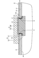
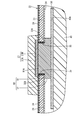
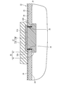
- the board 21 with a metal member includes a printed board 22 and a metal member 30 attached to the through hole 25 of the printed board 22.
- the printed circuit board 22 is a thick copper substrate having a large thickness of the conductive path 24 and capable of supplying a relatively large current to the conductive path 24.
- the printed circuit board 22 is made of an insulating plate 23 made of an insulating material such as copper by a printed wiring technique.
- Conductive paths 24 made of metal are formed on the upper and lower surfaces of the insulating plate 23.
- a through hole 25 is formed in the printed board 22 so as to penetrate in the vertical direction (plate thickness direction).
- the through hole 25 has a perfect circular shape, but is not limited thereto, and may be, for example, an elliptical shape, an oval shape, a polygonal shape, or the like.
- no conductive path is formed in the hole wall of the through hole 25, and the conductive path between the upper and lower surfaces of the printed circuit board 22 is electrically connected by a conductive bonding material 35 described later.
- the present invention is not limited to this.
- a conductive path is formed on the entire hole wall of the through hole 25 using copper foil or the like, and the conductive path 24 on the upper surface or the lower surface of the printed circuit board 22 is formed on the hole wall of the through hole 25. You may make it electrically connect with a conductive path.
- An electronic component 27 as a heat generating component is mounted on the conductive path 24 and the metal member 30 of the printed circuit board 22.
- the electronic component 27 has a flat rectangular parallelepiped main body 27A and a plurality of terminals 27B formed on the bottom surface of the main body 27A.
- the lower surfaces of the plurality of terminals 27 ⁇ / b> B are arranged on the same plane and are connected to a plurality of lands as conductive paths 24 formed on the surface of the printed circuit board 22.
- the conductive path 24 (land) connected to the terminal 27 ⁇ / b> B of the electronic component 27 includes a land 24 ⁇ / b> A (24) provided in a substantially rectangular area surrounding the substrate through-hole 25, and from this area.
- the plurality of terminals 27 ⁇ / b> B of the electronic component 27 of the present embodiment are soldered to the conductive path 24 (land 24 ⁇ / b> A, 24 ⁇ / b> B) on the upper surface of the printed circuit board 22 and the upper surface 31 ⁇ / b> A of the metal member 30.
- the electronic component 27 is an FET (Field Effect Transistor), but may be a resistor such as a shunt resistor or a heat generating component such as a coil or a capacitor.
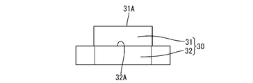
- the metal member 30 is made of, for example, a metal such as copper, copper alloy, aluminum, aluminum alloy, iron, and stainless steel, and as shown in FIGS. 4 and 5, a cylindrical shaft portion 31 that is inserted into the through hole 25. And a prismatic head portion 32 protruding in a stepped shape from the shaft portion 31. In the present embodiment, rivets are used as the metal member 30.
- the shaft portion 31 has a perfect circular cross section, and has a diameter B1 smaller than the hole diameter A1 of the through hole 25 as shown in FIG. 3. The shaft portion 31 is inserted into the through hole 25. Between the outer peripheral surface of the shaft portion 31 and the hole wall of the through hole 25, a gap G1 is formed in which solder as the bonding material 35 is disposed.
- the length in the vertical direction (axial direction) of the shaft portion 31 is larger than the thickness of the printed board 22 by the dimension of the gap G2 (the thickness of the bonding material 35), as shown in FIG.
- a bonding material 35 made of solder paste or the like applied in the vicinity of the through hole 25 on the lower surface of the printed circuit board 22.
- the bonding material 35 is filled into the gap G1 between the shaft portion 31 and the hole wall of the through hole 25 and the gap G2 between the printed board 22 and the head 32, and the printed board 22 and the metal member 30 are filled. And can be joined.
- the upper end surface 31 ⁇ / b> A of the shaft portion 31 is the same height (level) as the upper surface of the conductive path 24 on the upper surface of the printed circuit board 22.
- the head portion 32 has a rectangular plate shape, and the minimum diameter B2 passing through the central axis of the head portion 32 is larger than the hole diameter A1 of the through hole 25 as shown in FIG.
- the gap G ⁇ b> 2 between the upper surface 32 ⁇ / b> A of the head 32 and the lower surface of the printed circuit board 22 and the gap G ⁇ b> 1 between the outer peripheral surface of the shaft portion 31 and the hole wall of the through hole 25 include 35 is filled.
- a heat transfer material 36 is disposed between the lower surface of the head 32 and the upper surface 40A of the heat radiating member 40.
- the heat transfer material 36 has a high thermal conductivity such as silicone grease and has an insulating property. Material is used.
- the heat transfer material 36 is disposed in close contact with the entire lower surface of the head 32 and the upper surface 40 ⁇ / b> A of the heat radiating member 40. Thereby, the heat of the metal member 30 is transmitted to the heat radiating member 40 through the heat transfer material 36 and is radiated from the heat radiating member 40 to the outside.
- the heat dissipating member 40 is made of a metal having high thermal conductivity such as aluminum or aluminum alloy, and has a flat upper surface 40A as shown in FIG.
- the heat radiation fin 41 is provided.
- a plurality of spacer portions 42 projecting upward are provided on the upper surface 40 ⁇ / b> A of the heat radiating member 40.
- the plurality of spacer portions 42 are provided near the peripheral edge portion of the upper surface of the heat dissipation member 40, and the outer peripheral edge portion of the printed circuit board 22 is placed on and supports the printed circuit board 22, thereby radiating heat from the lower surface of the printed circuit board 22.
- a predetermined distance between the upper surface 40A of the member 40 (a dimension obtained by adding the thickness of the head 32 and the thickness of the heat transfer material 36) is maintained.
- the conductive path 24 is formed on the lower surface of the printed circuit board 22 that contacts the spacer section 42, an insulating layer made of an insulating adhesive or the like is formed on the upper surface of the spacer section 42, and the printed circuit board Insulate between the spacer 22 and the spacer portion 42.
- the circuit component 20 is formed by fixing the heat radiating member 40 and the metal member-equipped substrate 21 by a fixing means such as a screw (not shown), and the case 11 is put on the circuit component 20 to cover the electrical junction box 10 (FIG. 1). Is formed.
- the substrate 21 with a metal member has a printed circuit board 22 having a through hole 25, a shaft portion 31 inserted into the through hole 25, and a diameter B2 larger than the hole diameter A1 of the through hole 25, and is disposed outside the through hole 25.
- a metal member 30 having a head portion 32 and a conductive bonding material 35 for bonding the shaft portion 31 and the inner wall of the through hole 25.
- the shaft portion 31 of the metal member 30 and the inner wall of the through hole 25 of the printed board 22 are bonded by the conductive bonding material 35, for example, the shaft portion 31 of the metal member 30 only by press fitting.
- the metal member 30 has the head part 32 which has the diameter B2 larger than hole diameter A1 of the through-hole 25, it becomes possible to perform alignment of the insertion direction to the through-hole 25 of the axial part 31 easily. . Furthermore, by having the head part 32, the heat capacity of the metal member 30 can be increased compared with the case where there is no head part 32, and it becomes possible to improve heat dissipation.
- the upper end surface 31A (the end surface opposite to the head 32 side) of the shaft portion 31 inserted into the through hole 25 is the surface of the conductive path 24 on the printed circuit board 22 on which the electronic component 27 is mounted. It is formed at the same height. In this way, the step between the conductive path 24 of the printed circuit board 22 and the end surface 31A of the shaft portion 31 is suppressed, and thus the inclination of the electronic component 27 on the printed circuit board 22 is less likely to occur. Mounting defects can be reduced.
- the bonding material 35 bonds the surface of the printed circuit board 22 that faces the head 32 and the head 32 of the metal member 30. In this way, the contact area of the bonding material 35 is increased, so that the electrical resistance can be reduced while increasing the fixing force between the printed board 22 and the metal member 30. Further, the conductive path 24 on the lower surface of the printed circuit board 22 (the surface facing the head portion 32) and the head portion 32 can be electrically connected by the bonding material 35.
- the circuit component 20 overlaps the substrate 21 with a metal member, the electronic component 27 connected to the upper end surface 31A (the end surface opposite to the head 32 side) of the shaft portion 31, and the substrate 21 with the metal member. And a spacer portion 42 that maintains a distance between the printed board 22 and the heat radiating member 40. In this way, the heat of the electronic component 27 can be radiated by the heat radiating member 40, and the insertion depth of the metal member 30 into the through hole 25 of the shaft portion 31 can be appropriately adjusted by the spacer portion 42. It can be carried out.
- the spacer portion 42 is provided integrally with the heat radiating member 40. In this way, the number of parts can be reduced as compared with the case where the spacer portion 42 is provided separately from the heat dissipation member 40.
- Embodiment 2 will be described with reference to FIGS.
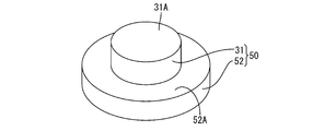
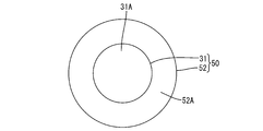
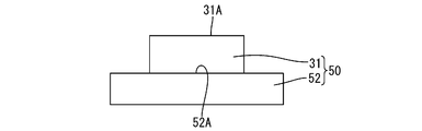
- the head 32 of the metal member 30 of the first embodiment has a rectangular shape, but in the second embodiment, as shown in FIG. 8, the head 52 of the metal member 50 has a circular shape. Since other configurations are the same as those in the above embodiment, the same components as those in the first embodiment are denoted by the same reference numerals and description thereof is omitted.
- the disk-shaped head portion 52 disposed below the through hole 25 in the printed circuit board 22 has a diameter B ⁇ b> 3 of the head portion 52 larger than the diameter A ⁇ b> 1 of the through hole 25.
- the gap between the through hole 25 and the shaft portion 31 of the printed circuit board 22 is bonded by the conductive bonding material 35, and the gap between the lower surface of the printed circuit board 22 and the upper surface 52A of the head 52 is electrically conductive. Bonding is performed with a bonding material 35 having a characteristic.
- Embodiment 3 will be described with reference to FIGS. 11 to 14.
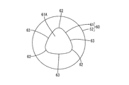
- FIG. 1 although the plane cross section of the axial part 31 of the metal member 30 was a perfect circle shape, in Embodiment 3, the axial part 61 of the metal member 60 is made into a non-circular shape. Since other configurations are the same as those in the above embodiment, the same components as those in the above embodiment are denoted by the same reference numerals and description thereof is omitted.
- the shaft portion 61 of the metal member 60 has a substantially triangular cross section, and the upper end surface 61 ⁇ / b> A of the shaft portion 61 is flush with the conductive path 24 on the upper surface of the printed circuit board 22. Is formed.
- the outer periphery of the shaft portion 61 is a tapered press-fit portion 62 that is press-fitted into the hole wall of the through-hole 25, and a non-press-fit portion 63 that is disposed to face the hole wall of the through-hole 25 and is not press-fitted into the hole wall of the through-hole 25. And have. As shown in FIG.
- the non-press-fit portion 63 forms a gap G3 in which the bonding material 35 is arranged between the hole wall of the through hole 25 and the gap G3 is filled with the bonding material 35 so that the metal member 60 is filled. And the printed circuit board 22 are joined.
- the metal member 60 can be temporarily locked to the hole wall of the through hole 25.
- the joining work can be easily performed, and the manufacturing cost can be reduced.
- the non-press-fit portion 63 is provided, a high dimensional accuracy is not required as compared with a configuration in which the entire outer periphery of the shaft portion 61 is press-fitted into the hole wall of the through hole 25, and thus the manufacturing cost can be reduced. .
- the fourth embodiment will be described with reference to FIGS. 15 and 16.
- the heat radiating member 40 was piled up under the printed circuit board 22, as for the electrical junction box 70 of Embodiment 4, the heat radiating member 40 is not piled up under the board
- the member-equipped substrate 21 is accommodated in the case 80 while being supported by the support member 71 from below.
- the support member 71 is a frame made of synthetic resin or metal, and includes a placement portion 72 on which the peripheral portion of the printed circuit board 22 is placed, and a locked portion that protrudes toward the case 80 and is locked to the case 80.
- the case 80 is made of metal or synthetic resin, and has an upper case 81 and a lower case 82, and a locking portion 84 through which the locked portion 73 is inserted and locked is formed.
- the fifth embodiment will be described with reference to FIGS. 17 and 18.
- the gap G2 in which the bonding material 35 is disposed is formed between the printed circuit board 22 and the head 32, but the shaft portion 91 of the metal member 90 in FIGS.
- the length is shorter than the shaft portion 31 of the first to third embodiments, and the upper surface 32A of the head portion 32 is in contact with the conductive path 24 on the lower surface of the printed circuit board 22. Since other configurations are the same as those in the above embodiment, the same components as those in the above embodiment are denoted by the same reference numerals and description thereof is omitted.
- the terminal 27B is arranged on the bottom surface of the main body 27A.
- the present invention is not limited to this.
- the terminal 27B protrudes from the side surface of the main body 27A and the conductive path 24 of the printed circuit board 22 It is good also as a structure soldered to the metal member 30.
- the heads 32 of the metal members 30, 50, 60 are plate-like, but are not limited to this, and may have a hemispherical or spherical head, for example. Further, for example, a convex shape in which a part of the head protrudes or a concave shape in which a part of the head is recessed may be used.
- the shaft portion 31 of the metal member 60 has a substantially triangular cross section, but is not limited thereto, and is a polygon other than a triangle, and the corner of the polygon is a hole wall of the through hole 25. It is good also as a press-fit part press-fitted in. Moreover, it is good also as a shape from which a diameter differs according to the position of the circumferential direction as an axial part which has major axis and minor axis, such as an ellipse and an ellipse shape.
- the number of electronic components 27 and metal members 30 is not limited to the number in the above embodiment, and the conductive path A plurality may be provided according to 24 or the like.
- the metal member 30 is a rivet, the present invention is not limited to this.
- the metal member 30 may be a screw having a screw portion formed on a shaft portion.
- the bonding material 35 is solder, but is not limited thereto, and may be, for example, a brazing material or a conductive adhesive (conductive resin). Further, for example, the metal member 30 may be temporarily fixed to the printed circuit board 22 (for example, the upper surface 32A of the head is fixed to the printed circuit board 22 with an adhesive) and then bonded with a bonding material.
Abstract
A metal member-equipped substrate 21 is provided with: a printed substrate 22 having a through-hole 25; a metal member 30 that has a shaft part 31 to be inserted in the through-hole 25 and a head part 32 that has a diameter B2 larger than the hole diameter A1 of the through-hole 25 and is disposed outside the through-hole 25; and a conductive joining material 35 that joins the shaft part 31 and the inner wall of the through-hole 25.
Description
本明細書では、金属部材付き基板に関する技術を開示する。
In this specification, the technique regarding the board | substrate with a metal member is disclosed.
従来、基板の貫通孔に金属部材が取付けられる技術が知られている。特許文献1の回路構成体は、矩形状の位置決め用貫通孔が形成されたプリント回路基板と、このプリント回路基板に積層されるバスバーとを備えており、バスバーに固定されたインレイは、プリント回路基板の位置決め用貫通孔に圧入されるようになっている。
Conventionally, a technique in which a metal member is attached to a through hole of a substrate is known. The circuit structure of Patent Document 1 includes a printed circuit board in which a rectangular positioning through-hole is formed, and a bus bar stacked on the printed circuit board. The inlay fixed to the bus bar is a printed circuit board. It is press-fitted into the positioning through hole of the substrate.
ところで、特許文献1の構成では、インレイをプリント回路基板の位置決め用貫通孔に圧入する構成であるため、インレイ及び位置決め用貫通孔の寸法に高い精度が必要とされ、製造コストが高くなりやすいという問題がある。
By the way, in the structure of patent document 1, since it is the structure which press-fits an inlay in the through-hole for positioning of a printed circuit board, high precision is required for the dimension of the inlay and the through-hole for positioning, and it says that manufacturing cost tends to become high. There's a problem.
本明細書に記載された技術は、上記のような事情に基づいて完成されたものであって、金属部材付き基板、回路構成体及び電気接続箱の製造コストを低減することを目的とする。
The technology described in the present specification has been completed based on the above-described circumstances, and aims to reduce the manufacturing costs of the substrate with metal member, the circuit structure, and the electrical junction box.
本明細書に記載された金属部材付き基板は、貫通孔を有するプリント基板と、前記貫通孔内に挿通される軸部と前記貫通孔の孔径よりも大きい径を有して前記貫通孔外に配される頭部とを有する金属部材と、前記軸部と前記貫通孔の内壁とを接合する導電性の接合材と、を備える。
上記構成によれば、金属部材の軸部とプリント基板の貫通孔の内壁とは導電性の接合材で接合されるため、例えば、圧入のみにより金属部材の軸部とプリント基板の貫通孔の内壁とを接続する構成と比較して、必ずしも高い寸法精度が必要ないため、製造コストを低減することができる。 The substrate with a metal member described in the present specification has a printed board having a through hole, a shaft portion inserted into the through hole, and a diameter larger than the hole diameter of the through hole, and is outside the through hole. A metal member having a head portion disposed thereon, and a conductive bonding material that bonds the shaft portion and the inner wall of the through hole.
According to the above configuration, the shaft portion of the metal member and the inner wall of the through hole of the printed circuit board are joined by the conductive bonding material. Compared with the configuration in which the two are connected, high dimensional accuracy is not necessarily required, so that the manufacturing cost can be reduced.
また、金属部材は、貫通孔の孔径よりも大きい径を有する頭部が基板の貫通孔外に配されるため、軸部の貫通孔への挿通方向の位置合わせを容易に行うことが可能になる。更に、金属部材が頭部を有することにより、金属部材に頭部がない場合と比較して金属部材の熱容量を高めることができるため、金属部材を介した放熱性を向上させることが可能になる。
In addition, since the metal member has a head having a diameter larger than the diameter of the through hole disposed outside the through hole of the substrate, it is possible to easily perform alignment in the insertion direction of the shaft portion to the through hole. Become. Furthermore, since the metal member has a head, the heat capacity of the metal member can be increased as compared with the case where the metal member does not have a head, and thus heat dissipation through the metal member can be improved. .
本明細書に記載された技術の実施態様としては以下の態様が好ましい。
前記貫通孔内に挿通された状態の前記軸部における前記頭部側とは反対側の端面は、前記プリント基板における電子部品が実装される前記導電路の表面と同じ高さに形成されている。
このようにすれば、基板の導電路における電子部品が実装される面と軸部の端面との間の段差が抑制されることにより、プリント基板上における電子部品の傾き等が生じにくくなり、電子部品の実装不良を低減することができる。 The following embodiments are preferable as the embodiments of the technology described in this specification.
An end surface opposite to the head side in the shaft portion inserted into the through hole is formed at the same height as the surface of the conductive path on which the electronic component on the printed board is mounted. .
In this way, the step between the surface on which the electronic component is mounted in the conductive path of the substrate and the end surface of the shaft portion is suppressed, so that the inclination of the electronic component on the printed circuit board is less likely to occur. Component mounting defects can be reduced.
前記接合材は、前記プリント基板における前記頭部に対向する面と前記金属部材の前記頭部とを接合する。
このようにすれば、接合材の接触面積が大きくなるため、基板と金属部材との間の固着力を高めつつ、電気抵抗を小さくすることができる。 The bonding material joins the surface of the printed circuit board facing the head and the head of the metal member.
In this way, since the contact area of the bonding material is increased, the electric resistance can be reduced while increasing the adhesion between the substrate and the metal member.
前記軸部の外周は、前記貫通孔の孔壁に圧入される圧入部と、前記貫通孔の孔壁に対向して配され、前記孔壁に圧入されない非圧入部と、を有する。
このようにすれば、貫通孔の孔壁に圧入可能な圧入部を有することにより、金属部材を取付ける際に軸部を貫通孔の孔壁に係止させた状態とすることが可能になるため、接合材で接合する作業を容易に行うことができ、製造コストを低減することができる。また、非圧入部を有することにより、軸部の外周の全面を貫通孔の孔壁に圧入する構成と比較して、高い寸法精度が必要ないため、製造コストを低減することができる。 The outer periphery of the shaft portion includes a press-fit portion that is press-fitted into the hole wall of the through-hole, and a non-press-fit portion that is disposed to face the hole wall of the through-hole and is not press-fitted into the hole wall.
In this way, by having a press-fit portion that can be press-fitted into the hole wall of the through hole, the shaft portion can be locked to the hole wall of the through hole when the metal member is attached. The operation of joining with the joining material can be easily performed, and the manufacturing cost can be reduced. In addition, by having the non-press-fit portion, compared with a configuration in which the entire outer periphery of the shaft portion is press-fitted into the hole wall of the through-hole, high dimensional accuracy is not required, and thus the manufacturing cost can be reduced.
前記金属部材付き基板と、前記軸部における前記頭部側とは反対側の端面に接続される電子部品と、前記金属部材付き基板に重ねられる放熱部材と、を備え、前記プリント基板と前記放熱部材との間隔を保持するスペーサ部を備える回路構成体とする。
このようにすれば、電子部品の熱を放熱部材により放熱させることができるとともに、スペーサ部により、基板の貫通孔に対する金属部材の軸部の挿通深さの位置合わせを適切に行うことができる。 The printed circuit board and the heat dissipation, comprising: the substrate with a metal member; an electronic component connected to an end surface of the shaft portion opposite to the head side; and a heat dissipation member superimposed on the substrate with the metal member. Let it be a circuit structure provided with the spacer part holding the space | interval with a member.
If it does in this way, while being able to radiate the heat of an electronic component with a heat radiating member, alignment of the penetration depth of the axial part of a metallic member to the penetration hole of a substrate can be performed appropriately by a spacer part.
前記スペーサ部は、前記放熱部材と一体に設けられている。
このようにすれば、スペーサ部を放熱部材とは別体で設ける場合と比較して部品点数を少なくすることができる。 The spacer portion is provided integrally with the heat dissipation member.
In this way, the number of parts can be reduced as compared with the case where the spacer portion is provided separately from the heat dissipation member.
このようにすれば、スペーサ部を放熱部材とは別体で設ける場合と比較して部品点数を少なくすることができる。 The spacer portion is provided integrally with the heat dissipation member.
In this way, the number of parts can be reduced as compared with the case where the spacer portion is provided separately from the heat dissipation member.
前記金属部材付き基板と、前記金属部材付き基板を覆うケースとを備える電気接続箱とする。
Suppose that it is an electrical junction box provided with the said board | substrate with a metal member, and the case which covers the said board | substrate with a metal member.
本明細書に記載された技術によれば、金属部材付き基板、回路構成体及び電気接続箱の製造コストを低減することが可能になる。
According to the technique described in this specification, it becomes possible to reduce the manufacturing cost of the substrate with metal member, the circuit structure, and the electrical junction box.
<実施形態1>
実施形態1について、図1~図6を参照しつつ説明する。
電気接続箱10は、例えば車両のバッテリ等の電源と、ランプ、ワイパー等の車載電装品やモータ等からなる負荷との間の電力供給経路に配され、例えばDC-DCコンバータやインバータ等に用いることができる。この電気接続箱10は任意の向きで配置することができるが、以下では、説明上、図3のX方向を前方、図1のY方向を左方、Z方向を上方として説明する。 <Embodiment 1>
The first embodiment will be described with reference to FIGS.
Theelectrical junction box 10 is arranged in a power supply path between a power source such as a battery of a vehicle and a load composed of an on-vehicle electrical component such as a lamp and a wiper or a motor, and is used for, for example, a DC-DC converter or an inverter. be able to. Although the electrical junction box 10 can be arranged in any orientation, for the sake of explanation, the X direction in FIG. 3 will be described as the front, the Y direction in FIG. 1 as the left, and the Z direction as the top.
実施形態1について、図1~図6を参照しつつ説明する。
電気接続箱10は、例えば車両のバッテリ等の電源と、ランプ、ワイパー等の車載電装品やモータ等からなる負荷との間の電力供給経路に配され、例えばDC-DCコンバータやインバータ等に用いることができる。この電気接続箱10は任意の向きで配置することができるが、以下では、説明上、図3のX方向を前方、図1のY方向を左方、Z方向を上方として説明する。 <Embodiment 1>
The first embodiment will be described with reference to FIGS.
The
(電気接続箱10)
電気接続箱10は、図1に示すように、回路構成体20と、回路構成体20を覆うケース11とを備えている。ケース11は、下方側が開口する箱形であって、アルミニウム、アルミニウム合金等の金属製又は合成樹脂製とされている。 (Electric junction box 10)
As shown in FIG. 1, theelectrical junction box 10 includes a circuit structure 20 and a case 11 that covers the circuit structure 20. The case 11 has a box shape with an opening on the lower side, and is made of metal such as aluminum or aluminum alloy or made of synthetic resin.
電気接続箱10は、図1に示すように、回路構成体20と、回路構成体20を覆うケース11とを備えている。ケース11は、下方側が開口する箱形であって、アルミニウム、アルミニウム合金等の金属製又は合成樹脂製とされている。 (Electric junction box 10)
As shown in FIG. 1, the
(回路構成体20)
回路構成体20は、金属部材付き基板21と、金属部材付き基板21の下に配され、金属部材付き基板21の熱を外部に放熱する放熱部材40とを備える。
(金属部材付き基板21)
金属部材付き基板21は、プリント基板22と、プリント基板22の貫通孔25に取付けられる金属部材30とを備える。
(プリント基板22)
プリント基板22は、導電路24の厚みが大きく、比較的大きな電流を導電路24に通電することが可能な厚銅基板であって、絶縁材料からなる絶縁板23にプリント配線技術により銅等の金属からなる導電路24が絶縁板23の上面及び下面に形成されている。プリント基板22には、貫通孔25が上下方向(板厚方向)に貫通形成されている。貫通孔25は、本実施形態では、真円形状とされているが、これに限られず、例えば、楕円形状、長円形状、多角形状等としてもよい。なお、本実施形態では、貫通孔25の孔壁には導電路が形成されておらず、後述する導電性の接合材35により、プリント基板22の上面や下面の導電路24間が電気的に接続されているが、これに限られず、例えば貫通孔25の孔壁の全体に銅箔等により導電路を形成し、プリント基板22の上面や下面の導電路24が貫通孔25の孔壁の導電路により電気的に接続されるようにしてもよい。 (Circuit structure 20)
Thecircuit component 20 includes a substrate 21 with a metal member and a heat radiating member 40 that is disposed under the substrate 21 with a metal member and radiates the heat of the substrate 21 with the metal member to the outside.
(Substrate with metal member 21)
Theboard 21 with a metal member includes a printed board 22 and a metal member 30 attached to the through hole 25 of the printed board 22.
(Printed circuit board 22)
The printedcircuit board 22 is a thick copper substrate having a large thickness of the conductive path 24 and capable of supplying a relatively large current to the conductive path 24. The printed circuit board 22 is made of an insulating plate 23 made of an insulating material such as copper by a printed wiring technique. Conductive paths 24 made of metal are formed on the upper and lower surfaces of the insulating plate 23. A through hole 25 is formed in the printed board 22 so as to penetrate in the vertical direction (plate thickness direction). In the present embodiment, the through hole 25 has a perfect circular shape, but is not limited thereto, and may be, for example, an elliptical shape, an oval shape, a polygonal shape, or the like. In the present embodiment, no conductive path is formed in the hole wall of the through hole 25, and the conductive path between the upper and lower surfaces of the printed circuit board 22 is electrically connected by a conductive bonding material 35 described later. However, the present invention is not limited to this. For example, a conductive path is formed on the entire hole wall of the through hole 25 using copper foil or the like, and the conductive path 24 on the upper surface or the lower surface of the printed circuit board 22 is formed on the hole wall of the through hole 25. You may make it electrically connect with a conductive path.
回路構成体20は、金属部材付き基板21と、金属部材付き基板21の下に配され、金属部材付き基板21の熱を外部に放熱する放熱部材40とを備える。
(金属部材付き基板21)
金属部材付き基板21は、プリント基板22と、プリント基板22の貫通孔25に取付けられる金属部材30とを備える。
(プリント基板22)
プリント基板22は、導電路24の厚みが大きく、比較的大きな電流を導電路24に通電することが可能な厚銅基板であって、絶縁材料からなる絶縁板23にプリント配線技術により銅等の金属からなる導電路24が絶縁板23の上面及び下面に形成されている。プリント基板22には、貫通孔25が上下方向(板厚方向)に貫通形成されている。貫通孔25は、本実施形態では、真円形状とされているが、これに限られず、例えば、楕円形状、長円形状、多角形状等としてもよい。なお、本実施形態では、貫通孔25の孔壁には導電路が形成されておらず、後述する導電性の接合材35により、プリント基板22の上面や下面の導電路24間が電気的に接続されているが、これに限られず、例えば貫通孔25の孔壁の全体に銅箔等により導電路を形成し、プリント基板22の上面や下面の導電路24が貫通孔25の孔壁の導電路により電気的に接続されるようにしてもよい。 (Circuit structure 20)
The
(Substrate with metal member 21)
The
(Printed circuit board 22)
The printed
プリント基板22の導電路24及び金属部材30には、発熱部品としての電子部品27が実装されている。電子部品27は、扁平な直方体状の本体27Aと、本体27Aの底面に形成された複数の端子27Bとを有する。複数の端子27Bの下面は、互いに同一平面上に配されており、プリント基板22の表面に形成された導電路24としての複数のランドに接続される。電子部品27の端子27Bに接続される導電路24(ランド)は、図3に示すように、概ね基板貫通孔25を囲む長方形状の領域に設けられたランド24A(24)と、この領域から離れた位置に一列に並んで配された複数のランド24B(24)とを有する。本実施形態の電子部品27の複数の端子27Bは、プリント基板22の上面の導電路24(ランド24A,24B))と、金属部材30の上面31Aとに半田付けされる。電子部品27は、本実施形態では、FET(Field Effect Transistor)とされているが、シャント抵抗等の抵抗、コイル、コンデンサ等の発熱部品としてもよい。
An electronic component 27 as a heat generating component is mounted on the conductive path 24 and the metal member 30 of the printed circuit board 22. The electronic component 27 has a flat rectangular parallelepiped main body 27A and a plurality of terminals 27B formed on the bottom surface of the main body 27A. The lower surfaces of the plurality of terminals 27 </ b> B are arranged on the same plane and are connected to a plurality of lands as conductive paths 24 formed on the surface of the printed circuit board 22. As shown in FIG. 3, the conductive path 24 (land) connected to the terminal 27 </ b> B of the electronic component 27 includes a land 24 </ b> A (24) provided in a substantially rectangular area surrounding the substrate through-hole 25, and from this area. And a plurality of lands 24B (24) arranged in a line at separate positions. The plurality of terminals 27 </ b> B of the electronic component 27 of the present embodiment are soldered to the conductive path 24 (land 24 </ b> A, 24 </ b> B) on the upper surface of the printed circuit board 22 and the upper surface 31 </ b> A of the metal member 30. In this embodiment, the electronic component 27 is an FET (Field Effect Transistor), but may be a resistor such as a shunt resistor or a heat generating component such as a coil or a capacitor.
(金属部材30)
金属部材30は、例えば、銅、銅合金、アルミニウム、アルミニウム合金、鉄、ステンレス鋼等の金属からなり、図4,図5に示すように、貫通孔25に挿通される円柱状の軸部31と、軸部31から段差状に張り出す角柱状の頭部32とを有する。本実施形態では、金属部材30としてリベットが用いられている。軸部31は、平断面が真円形状であって、図3に示すように、貫通孔25の孔径A1よりも小さい直径B1を有しており、貫通孔25に軸部31が挿通されると、軸部31の外周面と貫通孔25の孔壁との間には、接合材35としての半田が配される隙間G1が形成されている。 (Metal member 30)
Themetal member 30 is made of, for example, a metal such as copper, copper alloy, aluminum, aluminum alloy, iron, and stainless steel, and as shown in FIGS. 4 and 5, a cylindrical shaft portion 31 that is inserted into the through hole 25. And a prismatic head portion 32 protruding in a stepped shape from the shaft portion 31. In the present embodiment, rivets are used as the metal member 30. The shaft portion 31 has a perfect circular cross section, and has a diameter B1 smaller than the hole diameter A1 of the through hole 25 as shown in FIG. 3. The shaft portion 31 is inserted into the through hole 25. Between the outer peripheral surface of the shaft portion 31 and the hole wall of the through hole 25, a gap G1 is formed in which solder as the bonding material 35 is disposed.
金属部材30は、例えば、銅、銅合金、アルミニウム、アルミニウム合金、鉄、ステンレス鋼等の金属からなり、図4,図5に示すように、貫通孔25に挿通される円柱状の軸部31と、軸部31から段差状に張り出す角柱状の頭部32とを有する。本実施形態では、金属部材30としてリベットが用いられている。軸部31は、平断面が真円形状であって、図3に示すように、貫通孔25の孔径A1よりも小さい直径B1を有しており、貫通孔25に軸部31が挿通されると、軸部31の外周面と貫通孔25の孔壁との間には、接合材35としての半田が配される隙間G1が形成されている。 (Metal member 30)
The
軸部31の上下方向(軸方向)の長さは、図2に示されるように、プリント基板22の厚みよりも隙間G2の寸法(接合材35の厚み)だけ大きい。例えばプリント基板22の下面の貫通孔25の近傍に半田ペースト等からなる接合材35を塗布した状態で軸部31を貫通孔25に対して所定の位置(図2の位置)まで挿通することにより、軸部31と貫通孔25の孔壁との間の隙間G1と、プリント基板22と頭部32との間の隙間G2とに対して接合材35が充填され、プリント基板22と金属部材30とを接合することができる。金属部材30がプリント基板22に対して接合材35により接合された状態では、軸部31の上端面31Aがプリント基板22の上面の導電路24の上面と同じ高さ(面一)になる。頭部32は、矩形の板状であって、図3に示すように、頭部32の中心軸を通る最小の直径B2は、貫通孔25の孔径A1よりも大きい。図2に示すように、頭部32の上面32Aとプリント基板22の下面との間の隙間G2及び軸部31の外周面と貫通孔25の孔壁との間の隙間G1には、接合材35が充填されている。
The length in the vertical direction (axial direction) of the shaft portion 31 is larger than the thickness of the printed board 22 by the dimension of the gap G2 (the thickness of the bonding material 35), as shown in FIG. For example, by inserting the shaft portion 31 through the through hole 25 to a predetermined position (the position in FIG. 2) with a bonding material 35 made of solder paste or the like applied in the vicinity of the through hole 25 on the lower surface of the printed circuit board 22. The bonding material 35 is filled into the gap G1 between the shaft portion 31 and the hole wall of the through hole 25 and the gap G2 between the printed board 22 and the head 32, and the printed board 22 and the metal member 30 are filled. And can be joined. In a state where the metal member 30 is bonded to the printed circuit board 22 by the bonding material 35, the upper end surface 31 </ b> A of the shaft portion 31 is the same height (level) as the upper surface of the conductive path 24 on the upper surface of the printed circuit board 22. The head portion 32 has a rectangular plate shape, and the minimum diameter B2 passing through the central axis of the head portion 32 is larger than the hole diameter A1 of the through hole 25 as shown in FIG. As shown in FIG. 2, the gap G <b> 2 between the upper surface 32 </ b> A of the head 32 and the lower surface of the printed circuit board 22 and the gap G <b> 1 between the outer peripheral surface of the shaft portion 31 and the hole wall of the through hole 25 include 35 is filled.
頭部32の下面と放熱部材40の上面40Aとの間には、伝熱材36が配されている、伝熱材36は、例えば、シリコーングリスなどの熱伝導性が高く、絶縁性を有する材料が用いられている。伝熱材36は、頭部32の下面の全体と放熱部材40の上面40Aとに密着するように配される。これにより、金属部材30の熱は伝熱材36を介して放熱部材40に伝わり、放熱部材40から外部に放熱される。
A heat transfer material 36 is disposed between the lower surface of the head 32 and the upper surface 40A of the heat radiating member 40. The heat transfer material 36 has a high thermal conductivity such as silicone grease and has an insulating property. Material is used. The heat transfer material 36 is disposed in close contact with the entire lower surface of the head 32 and the upper surface 40 </ b> A of the heat radiating member 40. Thereby, the heat of the metal member 30 is transmitted to the heat radiating member 40 through the heat transfer material 36 and is radiated from the heat radiating member 40 to the outside.
(放熱部材40)
放熱部材40はアルミニウム、アルミニウム合金等の熱伝導性が高い金属類製であって、図1に示すように、平坦な上面40Aを有し、下面側に櫛刃状に並んで配された複数の放熱フィン41を有している。放熱部材40の上面40Aには、上方に突出する複数のスペーサ部42が設けられている。複数のスペーサ部42は、放熱部材40の上面における周縁部寄りに設けられており、プリント基板22の外周縁部が載置されてプリント基板22を支持することにより、プリント基板22の下面と放熱部材40の上面40Aとの間の所定の間隔(頭部32の厚みと伝熱材36の厚みを加えた寸法)を保持する。なお、スペーサ部42に接触するプリント基板22の下面に導電路24が形成されている場合には、スペーサ部42の上面には、絶縁性の接着剤等からなる絶縁層が形成され、プリント基板22とスペーサ部42との間を絶縁する。放熱部材40と金属部材付き基板21とを図示しないネジ等の固定手段により固定することで回路構成体20が形成され、回路構成体20にケース11を被せることにより電気接続箱10(図1)が形成される。 (Heat dissipation member 40)
Theheat dissipating member 40 is made of a metal having high thermal conductivity such as aluminum or aluminum alloy, and has a flat upper surface 40A as shown in FIG. The heat radiation fin 41 is provided. A plurality of spacer portions 42 projecting upward are provided on the upper surface 40 </ b> A of the heat radiating member 40. The plurality of spacer portions 42 are provided near the peripheral edge portion of the upper surface of the heat dissipation member 40, and the outer peripheral edge portion of the printed circuit board 22 is placed on and supports the printed circuit board 22, thereby radiating heat from the lower surface of the printed circuit board 22. A predetermined distance between the upper surface 40A of the member 40 (a dimension obtained by adding the thickness of the head 32 and the thickness of the heat transfer material 36) is maintained. When the conductive path 24 is formed on the lower surface of the printed circuit board 22 that contacts the spacer section 42, an insulating layer made of an insulating adhesive or the like is formed on the upper surface of the spacer section 42, and the printed circuit board Insulate between the spacer 22 and the spacer portion 42. The circuit component 20 is formed by fixing the heat radiating member 40 and the metal member-equipped substrate 21 by a fixing means such as a screw (not shown), and the case 11 is put on the circuit component 20 to cover the electrical junction box 10 (FIG. 1). Is formed.
放熱部材40はアルミニウム、アルミニウム合金等の熱伝導性が高い金属類製であって、図1に示すように、平坦な上面40Aを有し、下面側に櫛刃状に並んで配された複数の放熱フィン41を有している。放熱部材40の上面40Aには、上方に突出する複数のスペーサ部42が設けられている。複数のスペーサ部42は、放熱部材40の上面における周縁部寄りに設けられており、プリント基板22の外周縁部が載置されてプリント基板22を支持することにより、プリント基板22の下面と放熱部材40の上面40Aとの間の所定の間隔(頭部32の厚みと伝熱材36の厚みを加えた寸法)を保持する。なお、スペーサ部42に接触するプリント基板22の下面に導電路24が形成されている場合には、スペーサ部42の上面には、絶縁性の接着剤等からなる絶縁層が形成され、プリント基板22とスペーサ部42との間を絶縁する。放熱部材40と金属部材付き基板21とを図示しないネジ等の固定手段により固定することで回路構成体20が形成され、回路構成体20にケース11を被せることにより電気接続箱10(図1)が形成される。 (Heat dissipation member 40)
The
本実施形態によれば、以下の作用、効果を奏する。
金属部材付き基板21は、貫通孔25を有するプリント基板22と、貫通孔25内に挿通される軸部31と貫通孔25の孔径A1よりも大きい径B2を有して貫通孔25外に配される頭部32とを有する金属部材30と、軸部31と貫通孔25の内壁とを接合する導電性の接合材35と、を備える。
本実施形態によれば、金属部材30の軸部31とプリント基板22の貫通孔25の内壁とは導電性の接合材35で接合されるため、例えば、圧入のみにより金属部材30の軸部31とプリント基板22の貫通孔25の内壁とを接続する構成と比較して、必ずしも高い寸法精度が必要ないため、製造コストを低減することができる。また、金属部材30は、貫通孔25の孔径A1よりも大きい径B2を有する頭部32を有するため、軸部31の貫通孔25への挿通方向の位置合わせを容易に行うことが可能になる。更に、頭部32を有することにより、頭部32がない場合と比較して金属部材30の熱容量を高めることができ、放熱性を向上させることが可能になる。 According to this embodiment, the following operations and effects are achieved.
Thesubstrate 21 with a metal member has a printed circuit board 22 having a through hole 25, a shaft portion 31 inserted into the through hole 25, and a diameter B2 larger than the hole diameter A1 of the through hole 25, and is disposed outside the through hole 25. A metal member 30 having a head portion 32 and a conductive bonding material 35 for bonding the shaft portion 31 and the inner wall of the through hole 25.
According to the present embodiment, since theshaft portion 31 of the metal member 30 and the inner wall of the through hole 25 of the printed board 22 are bonded by the conductive bonding material 35, for example, the shaft portion 31 of the metal member 30 only by press fitting. Compared with the structure which connects the inner wall of the through-hole 25 of the printed circuit board 22 and a high dimensional accuracy is not necessarily required, manufacturing cost can be reduced. Moreover, since the metal member 30 has the head part 32 which has the diameter B2 larger than hole diameter A1 of the through-hole 25, it becomes possible to perform alignment of the insertion direction to the through-hole 25 of the axial part 31 easily. . Furthermore, by having the head part 32, the heat capacity of the metal member 30 can be increased compared with the case where there is no head part 32, and it becomes possible to improve heat dissipation.
金属部材付き基板21は、貫通孔25を有するプリント基板22と、貫通孔25内に挿通される軸部31と貫通孔25の孔径A1よりも大きい径B2を有して貫通孔25外に配される頭部32とを有する金属部材30と、軸部31と貫通孔25の内壁とを接合する導電性の接合材35と、を備える。
本実施形態によれば、金属部材30の軸部31とプリント基板22の貫通孔25の内壁とは導電性の接合材35で接合されるため、例えば、圧入のみにより金属部材30の軸部31とプリント基板22の貫通孔25の内壁とを接続する構成と比較して、必ずしも高い寸法精度が必要ないため、製造コストを低減することができる。また、金属部材30は、貫通孔25の孔径A1よりも大きい径B2を有する頭部32を有するため、軸部31の貫通孔25への挿通方向の位置合わせを容易に行うことが可能になる。更に、頭部32を有することにより、頭部32がない場合と比較して金属部材30の熱容量を高めることができ、放熱性を向上させることが可能になる。 According to this embodiment, the following operations and effects are achieved.
The
According to the present embodiment, since the
また、貫通孔25内に挿通された状態の軸部31の上端面31A(頭部32側とは反対側の端面)は、プリント基板22における電子部品27が実装される導電路24の表面と同じ高さに形成されている。
このようにすれば、プリント基板22の導電路24と軸部31の端面31Aとの間の段差が抑制されるため、プリント基板22上における電子部品27の傾き等が生じにくくなり、電子部品27の実装不良を低減することができる。 Further, theupper end surface 31A (the end surface opposite to the head 32 side) of the shaft portion 31 inserted into the through hole 25 is the surface of the conductive path 24 on the printed circuit board 22 on which the electronic component 27 is mounted. It is formed at the same height.
In this way, the step between theconductive path 24 of the printed circuit board 22 and the end surface 31A of the shaft portion 31 is suppressed, and thus the inclination of the electronic component 27 on the printed circuit board 22 is less likely to occur. Mounting defects can be reduced.
このようにすれば、プリント基板22の導電路24と軸部31の端面31Aとの間の段差が抑制されるため、プリント基板22上における電子部品27の傾き等が生じにくくなり、電子部品27の実装不良を低減することができる。 Further, the
In this way, the step between the
接合材35は、プリント基板22における頭部32に対向する面と金属部材30の頭部32とを接合する。
このようにすれば、接合材35の接触面積が大きくなるため、プリント基板22と金属部材30との間の固着力を高めつつ、電気抵抗を小さくすることができる。また、プリント基板22の下面(頭部32に対向する面)の導電路24と頭部32とを接合材35により電気的に接続することができる。 Thebonding material 35 bonds the surface of the printed circuit board 22 that faces the head 32 and the head 32 of the metal member 30.
In this way, the contact area of thebonding material 35 is increased, so that the electrical resistance can be reduced while increasing the fixing force between the printed board 22 and the metal member 30. Further, the conductive path 24 on the lower surface of the printed circuit board 22 (the surface facing the head portion 32) and the head portion 32 can be electrically connected by the bonding material 35.
このようにすれば、接合材35の接触面積が大きくなるため、プリント基板22と金属部材30との間の固着力を高めつつ、電気抵抗を小さくすることができる。また、プリント基板22の下面(頭部32に対向する面)の導電路24と頭部32とを接合材35により電気的に接続することができる。 The
In this way, the contact area of the
また、回路構成体20は、金属部材付き基板21と、軸部31における上端面31A(頭部32側とは反対側の端面)に接続される電子部品27と、金属部材付き基板21に重ねられる放熱部材40と、を備え、プリント基板22と放熱部材40との間隔を保持するスペーサ部42を備える。
このようにすれば、電子部品27の熱を放熱部材40により放熱することができるとともに、スペーサ部42により、金属部材30の軸部31の貫通孔25への挿通深さの位置合わせを適切に行うことができる。 In addition, thecircuit component 20 overlaps the substrate 21 with a metal member, the electronic component 27 connected to the upper end surface 31A (the end surface opposite to the head 32 side) of the shaft portion 31, and the substrate 21 with the metal member. And a spacer portion 42 that maintains a distance between the printed board 22 and the heat radiating member 40.
In this way, the heat of theelectronic component 27 can be radiated by the heat radiating member 40, and the insertion depth of the metal member 30 into the through hole 25 of the shaft portion 31 can be appropriately adjusted by the spacer portion 42. It can be carried out.
このようにすれば、電子部品27の熱を放熱部材40により放熱することができるとともに、スペーサ部42により、金属部材30の軸部31の貫通孔25への挿通深さの位置合わせを適切に行うことができる。 In addition, the
In this way, the heat of the
また、スペーサ部42は、放熱部材40と一体に設けられている。
このようにすれば、スペーサ部42を放熱部材40とは別体で設ける場合と比較して部品点数を少なくすることができる。 Thespacer portion 42 is provided integrally with the heat radiating member 40.
In this way, the number of parts can be reduced as compared with the case where thespacer portion 42 is provided separately from the heat dissipation member 40.
このようにすれば、スペーサ部42を放熱部材40とは別体で設ける場合と比較して部品点数を少なくすることができる。 The
In this way, the number of parts can be reduced as compared with the case where the
<実施形態2>
次に、実施形態2を図7~図10を参照して説明する。実施形態1の金属部材30の頭部32は、矩形状であったが、実施形態2は、図8に示すように、金属部材50の頭部52を円形状とするものである。他の構成は、上記実施形態と同一であるため、以下では、実施形態1と同一の構成については同一の符号を付して説明を省略する。 <Embodiment 2>
Next,Embodiment 2 will be described with reference to FIGS. The head 32 of the metal member 30 of the first embodiment has a rectangular shape, but in the second embodiment, as shown in FIG. 8, the head 52 of the metal member 50 has a circular shape. Since other configurations are the same as those in the above embodiment, the same components as those in the first embodiment are denoted by the same reference numerals and description thereof is omitted.
次に、実施形態2を図7~図10を参照して説明する。実施形態1の金属部材30の頭部32は、矩形状であったが、実施形態2は、図8に示すように、金属部材50の頭部52を円形状とするものである。他の構成は、上記実施形態と同一であるため、以下では、実施形態1と同一の構成については同一の符号を付して説明を省略する。 <
Next,
プリント基板22における貫通孔25の下方に配された円板状の頭部52は、図7に示すように、頭部52の直径B3は、貫通孔25の直径A1よりも大きくされている。プリント基板22の貫通孔25と軸部31との間の隙間は、導電性の接合材35で接合されるとともに、プリント基板22の下面と頭部52の上面52Aとの間の隙間は、導電性の接合材35で接合される。
As shown in FIG. 7, the disk-shaped head portion 52 disposed below the through hole 25 in the printed circuit board 22 has a diameter B <b> 3 of the head portion 52 larger than the diameter A <b> 1 of the through hole 25. The gap between the through hole 25 and the shaft portion 31 of the printed circuit board 22 is bonded by the conductive bonding material 35, and the gap between the lower surface of the printed circuit board 22 and the upper surface 52A of the head 52 is electrically conductive. Bonding is performed with a bonding material 35 having a characteristic.
<実施形態3>
実施形態3について、図11~図14を参照して説明する。上記実施形態では、金属部材30の軸部31の平断面は真円形状であったが、実施形態3では、金属部材60の軸部61が非円形状とされるものである。他の構成は、上記実施形態と同一であるため、以下では、上記実施形態と同一の構成については同一の符号を付して説明を省略する。 <Embodiment 3>
Embodiment 3 will be described with reference to FIGS. 11 to 14. FIG. In the said embodiment, although the plane cross section of theaxial part 31 of the metal member 30 was a perfect circle shape, in Embodiment 3, the axial part 61 of the metal member 60 is made into a non-circular shape. Since other configurations are the same as those in the above embodiment, the same components as those in the above embodiment are denoted by the same reference numerals and description thereof is omitted.
実施形態3について、図11~図14を参照して説明する。上記実施形態では、金属部材30の軸部31の平断面は真円形状であったが、実施形態3では、金属部材60の軸部61が非円形状とされるものである。他の構成は、上記実施形態と同一であるため、以下では、上記実施形態と同一の構成については同一の符号を付して説明を省略する。 <Embodiment 3>
Embodiment 3 will be described with reference to FIGS. 11 to 14. FIG. In the said embodiment, although the plane cross section of the
金属部材60の軸部61は、図12,図13に示すように、平断面が略三角形状であって、軸部61の上端面61Aは、プリント基板22の上面の導電路24と面一に形成されている。軸部61の外周は、貫通孔25の孔壁に圧入される先細の圧入部62と、貫通孔25の孔壁に対向して配され、貫通孔25の孔壁に圧入されない非圧入部63とを有する。非圧入部63は、図11に示すように、貫通孔25の孔壁との間に接合材35が配される隙間G3を形成し、この隙間G3に接合材35が充填されて金属部材60とプリント基板22とが接合される。
As shown in FIGS. 12 and 13, the shaft portion 61 of the metal member 60 has a substantially triangular cross section, and the upper end surface 61 </ b> A of the shaft portion 61 is flush with the conductive path 24 on the upper surface of the printed circuit board 22. Is formed. The outer periphery of the shaft portion 61 is a tapered press-fit portion 62 that is press-fitted into the hole wall of the through-hole 25, and a non-press-fit portion 63 that is disposed to face the hole wall of the through-hole 25 and is not press-fitted into the hole wall of the through-hole 25. And have. As shown in FIG. 11, the non-press-fit portion 63 forms a gap G3 in which the bonding material 35 is arranged between the hole wall of the through hole 25 and the gap G3 is filled with the bonding material 35 so that the metal member 60 is filled. And the printed circuit board 22 are joined.
実施形態3によれば、圧入部62が貫通孔25の孔壁に圧入されることにより、金属部材60を貫通孔25の孔壁に仮係止することが可能になるため、接合材35で接合する作業を容易に行うことができ、製造コストを低減することが可能になる。また、非圧入部63を有することにより、軸部61の外周の全面を貫通孔25の孔壁に圧入する構成と比較して、高い寸法精度が必要なくなるため、製造コストを低減することができる。
According to the third embodiment, since the press-fitting portion 62 is press-fitted into the hole wall of the through hole 25, the metal member 60 can be temporarily locked to the hole wall of the through hole 25. The joining work can be easily performed, and the manufacturing cost can be reduced. In addition, since the non-press-fit portion 63 is provided, a high dimensional accuracy is not required as compared with a configuration in which the entire outer periphery of the shaft portion 61 is press-fitted into the hole wall of the through hole 25, and thus the manufacturing cost can be reduced. .
<実施形態4>
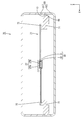
実施形態4について、図15,図16を参照して説明する。上記実施形態では、プリント基板22の下に放熱部材40が重ねられていたが、実施形態4の電気接続箱70は、金属部材付き基板21の下に放熱部材40が重ねられておらず、金属部材付き基板21は、支持部材71に下側から支持された状態でケース80に収容されている。支持部材71は、合成樹脂製又は金属製のフレームであって、プリント基板22の周縁部が載置される載置部72と、ケース80側に突出してケース80に係止される被係止部73とを有する。ケース80は、金属製又は合成樹脂製であって、アッパーケース81とロアケース82とを有し、被係止部73が挿通されて係止される係止部84が貫通形成されている。 <Embodiment 4>
The fourth embodiment will be described with reference to FIGS. 15 and 16. In the said embodiment, although theheat radiating member 40 was piled up under the printed circuit board 22, as for the electrical junction box 70 of Embodiment 4, the heat radiating member 40 is not piled up under the board | substrate 21 with a metal member, but metal The member-equipped substrate 21 is accommodated in the case 80 while being supported by the support member 71 from below. The support member 71 is a frame made of synthetic resin or metal, and includes a placement portion 72 on which the peripheral portion of the printed circuit board 22 is placed, and a locked portion that protrudes toward the case 80 and is locked to the case 80. Part 73. The case 80 is made of metal or synthetic resin, and has an upper case 81 and a lower case 82, and a locking portion 84 through which the locked portion 73 is inserted and locked is formed.
実施形態4について、図15,図16を参照して説明する。上記実施形態では、プリント基板22の下に放熱部材40が重ねられていたが、実施形態4の電気接続箱70は、金属部材付き基板21の下に放熱部材40が重ねられておらず、金属部材付き基板21は、支持部材71に下側から支持された状態でケース80に収容されている。支持部材71は、合成樹脂製又は金属製のフレームであって、プリント基板22の周縁部が載置される載置部72と、ケース80側に突出してケース80に係止される被係止部73とを有する。ケース80は、金属製又は合成樹脂製であって、アッパーケース81とロアケース82とを有し、被係止部73が挿通されて係止される係止部84が貫通形成されている。 <Embodiment 4>
The fourth embodiment will be described with reference to FIGS. 15 and 16. In the said embodiment, although the
<実施形態5>
実施形態5について、図17,図18を参照して説明する。実施形態1~3では、プリント基板22と頭部32との間には接合材35が配される隙間G2が形成されていたが、図17,図18の金属部材90の軸部91は、実施形態1~3の軸部31よりも短くされており、頭部32の上面32Aがプリント基板22の下面の導電路24に当接するものである。他の構成は、上記実施形態と同一であるため、以下では、上記実施形態と同一の構成については同一の符号を付して説明を省略する。 <Embodiment 5>
The fifth embodiment will be described with reference to FIGS. 17 and 18. In the first to third embodiments, the gap G2 in which thebonding material 35 is disposed is formed between the printed circuit board 22 and the head 32, but the shaft portion 91 of the metal member 90 in FIGS. The length is shorter than the shaft portion 31 of the first to third embodiments, and the upper surface 32A of the head portion 32 is in contact with the conductive path 24 on the lower surface of the printed circuit board 22. Since other configurations are the same as those in the above embodiment, the same components as those in the above embodiment are denoted by the same reference numerals and description thereof is omitted.
実施形態5について、図17,図18を参照して説明する。実施形態1~3では、プリント基板22と頭部32との間には接合材35が配される隙間G2が形成されていたが、図17,図18の金属部材90の軸部91は、実施形態1~3の軸部31よりも短くされており、頭部32の上面32Aがプリント基板22の下面の導電路24に当接するものである。他の構成は、上記実施形態と同一であるため、以下では、上記実施形態と同一の構成については同一の符号を付して説明を省略する。 <Embodiment 5>
The fifth embodiment will be described with reference to FIGS. 17 and 18. In the first to third embodiments, the gap G2 in which the
<他の実施形態>
本明細書に記載された技術は上記記述及び図面によって説明した実施形態に限定されるものではなく、例えば次のような実施形態も本明細書に記載された技術の技術的範囲に含まれる。
(1)電子部品27は、本体27Aの底面に端子27Bが配されるものとしたが、これに限られず、例えば、本体27Aの側面等から端子27Bが突出してプリント基板22の導電路24や金属部材30に半田付けされる構成としてもよい。 <Other embodiments>
The technology described in the present specification is not limited to the embodiments described with reference to the above description and the drawings. For example, the following embodiments are also included in the technical scope of the technology described in the present specification.
(1) In theelectronic component 27, the terminal 27B is arranged on the bottom surface of the main body 27A. However, the present invention is not limited to this. For example, the terminal 27B protrudes from the side surface of the main body 27A and the conductive path 24 of the printed circuit board 22 It is good also as a structure soldered to the metal member 30. FIG.
本明細書に記載された技術は上記記述及び図面によって説明した実施形態に限定されるものではなく、例えば次のような実施形態も本明細書に記載された技術の技術的範囲に含まれる。
(1)電子部品27は、本体27Aの底面に端子27Bが配されるものとしたが、これに限られず、例えば、本体27Aの側面等から端子27Bが突出してプリント基板22の導電路24や金属部材30に半田付けされる構成としてもよい。 <Other embodiments>
The technology described in the present specification is not limited to the embodiments described with reference to the above description and the drawings. For example, the following embodiments are also included in the technical scope of the technology described in the present specification.
(1) In the
(2)金属部材30,50,60の頭部32は、板状であったが、これに限られず、例えば、半球状や球状の頭部を有する構成としてもよい。また、例えば、頭部の一部が突出する凸形状や頭部の一部が凹んだ凹形状としてもよい。
(3)実施形態3では、金属部材60の軸部31は、断面が略三角形状としたが、これに限られず、三角形以外の多角形とし、多角形の角部が貫通孔25の孔壁に圧入される圧入部としてもよい。また、楕円形や長円形状等の長径と短径とを有する軸部として、周方向の位置に応じて直径の異なる形状としてもよい。 (2) Theheads 32 of the metal members 30, 50, 60 are plate-like, but are not limited to this, and may have a hemispherical or spherical head, for example. Further, for example, a convex shape in which a part of the head protrudes or a concave shape in which a part of the head is recessed may be used.
(3) In the third embodiment, theshaft portion 31 of the metal member 60 has a substantially triangular cross section, but is not limited thereto, and is a polygon other than a triangle, and the corner of the polygon is a hole wall of the through hole 25. It is good also as a press-fit part press-fitted in. Moreover, it is good also as a shape from which a diameter differs according to the position of the circumferential direction as an axial part which has major axis and minor axis, such as an ellipse and an ellipse shape.
(3)実施形態3では、金属部材60の軸部31は、断面が略三角形状としたが、これに限られず、三角形以外の多角形とし、多角形の角部が貫通孔25の孔壁に圧入される圧入部としてもよい。また、楕円形や長円形状等の長径と短径とを有する軸部として、周方向の位置に応じて直径の異なる形状としてもよい。 (2) The
(3) In the third embodiment, the
(4)図1,図15では、1つの電子部品27や1つの金属部材30が示されているが、電子部品27や金属部材30の数は、上記実施形態の数に限られず、導電路24等に応じて複数設けてもよい。
(5)金属部材30はリベットとしたが、これに限られず、例えば、軸部にネジ部が形成されたネジとしてもよい。 (4) Although oneelectronic component 27 and one metal member 30 are shown in FIGS. 1 and 15, the number of electronic components 27 and metal members 30 is not limited to the number in the above embodiment, and the conductive path A plurality may be provided according to 24 or the like.
(5) Although themetal member 30 is a rivet, the present invention is not limited to this. For example, the metal member 30 may be a screw having a screw portion formed on a shaft portion.
(5)金属部材30はリベットとしたが、これに限られず、例えば、軸部にネジ部が形成されたネジとしてもよい。 (4) Although one
(5) Although the
(6)接合材35は、半田としたが、これに限られず、例えばロウ材や導電性接着剤(導電性樹脂)としてもよい。また、例えば金属部材30をプリント基板22に対して仮止め(例えば頭部の上面32Aを接着剤でプリント基板22に固定)した後に接合材で接合してもよい。
(6) The bonding material 35 is solder, but is not limited thereto, and may be, for example, a brazing material or a conductive adhesive (conductive resin). Further, for example, the metal member 30 may be temporarily fixed to the printed circuit board 22 (for example, the upper surface 32A of the head is fixed to the printed circuit board 22 with an adhesive) and then bonded with a bonding material.
10,70: 電気接続箱
11,80: ケース
20: 回路構成体
21: 金属部材付き基板
22: プリント基板
23: 絶縁板
24: 導電路
25: 貫通孔
27: 電子部品
30,50,60: 金属部材
30: 金属部材
31,61: 軸部
31A: 端面
32,52: 頭部
32A,52A: 上面
35: 接合材
36: 放熱グリス
40: 放熱部材
42: スペーサ部
62: 圧入部
63: 非圧入部
A1: 貫通孔の孔径
B1: 軸部の径
B2: 頭部の径
B3: 頭部の径
G1,G2,G3: 隙間 10, 70:Electrical connection box 11, 80: Case 20: Circuit component 21: Substrate with metal member 22: Printed circuit board 23: Insulating plate 24: Conductive path 25: Through hole 27: Electronic component 30, 50, 60: Metal Member 30: Metal member 31, 61: Shaft portion 31A: End surface 32, 52: Head portion 32A, 52A: Upper surface 35: Bonding material 36: Heat radiation grease 40: Heat radiation member 42: Spacer portion 62: Press fit portion 63: Non press fit portion A1: Hole diameter B1 of the through hole B1: Shaft diameter B2: Head diameter B3: Head diameter G1, G2, G3: Gap
11,80: ケース
20: 回路構成体
21: 金属部材付き基板
22: プリント基板
23: 絶縁板
24: 導電路
25: 貫通孔
27: 電子部品
30,50,60: 金属部材
30: 金属部材
31,61: 軸部
31A: 端面
32,52: 頭部
32A,52A: 上面
35: 接合材
36: 放熱グリス
40: 放熱部材
42: スペーサ部
62: 圧入部
63: 非圧入部
A1: 貫通孔の孔径
B1: 軸部の径
B2: 頭部の径
B3: 頭部の径
G1,G2,G3: 隙間 10, 70:
Claims (7)
- 貫通孔を有するプリント基板と、
前記貫通孔内に挿通される軸部と前記貫通孔の孔径よりも大きい径を有して前記貫通孔外に配される頭部とを有する金属部材と、
前記軸部と前記貫通孔の内壁とを接合する導電性の接合材と、を備える金属部材付き基板。 A printed circuit board having a through hole;
A metal member having a shaft portion inserted into the through hole and a head portion having a diameter larger than the hole diameter of the through hole and disposed outside the through hole;
A substrate with a metal member, comprising: a conductive bonding material that bonds the shaft portion and the inner wall of the through hole. - 前記貫通孔内に挿通された状態の前記軸部における前記頭部側とは反対側の端面は、前記プリント基板における電子部品が実装される導電路の表面と同じ高さに形成されている請求項1に記載の金属部材付き基板。 The end surface on the opposite side to the head side in the shaft portion inserted into the through hole is formed at the same height as the surface of the conductive path on which the electronic component is mounted on the printed circuit board. Item 2. A substrate with a metal member according to Item 1.
- 前記接合材は、前記プリント基板における前記頭部に対向する面と前記金属部材の前記頭部とを接合する請求項1又は請求項2に記載の金属部材付き基板。 The board | substrate with a metal member of Claim 1 or Claim 2 in which the said joining material joins the surface facing the said head in the said printed circuit board, and the said head of the said metal member.
- 前記軸部の外周は、前記貫通孔の孔壁に圧入される圧入部と、前記貫通孔の孔壁に対向して配され、前記孔壁に圧入されない非圧入部と、を有する請求項1から請求項3のいずれか一項に記載の金属部材付き基板。 The outer periphery of the shaft portion includes a press-fit portion that is press-fitted into the hole wall of the through-hole, and a non-press-fit portion that is arranged to face the hole wall of the through-hole and is not press-fitted into the hole wall. The board | substrate with a metal member as described in any one of Claim 3.
- 請求項1から請求項4のいずれか一項に記載の金属部材付き基板と、
前記軸部における前記頭部側とは反対側の端面に接続される電子部品と、
前記金属部材付き基板に重ねられる放熱部材と、を備え、
前記プリント基板と前記放熱部材との間隔を保持するスペーサ部を備える、回路構成体。 A substrate with a metal member according to any one of claims 1 to 4,
An electronic component connected to an end surface of the shaft portion opposite to the head side;
A heat dissipating member overlaid on the substrate with the metal member,
A circuit structure comprising a spacer portion that maintains a distance between the printed circuit board and the heat dissipation member. - 前記スペーサ部は、前記放熱部材と一体に設けられている、請求項5に記載の回路構成体。 The circuit configuration body according to claim 5, wherein the spacer portion is provided integrally with the heat dissipation member.
- 請求項1から請求項6のいずれか一項に記載の金属部材付き基板と、前記金属部材付き基板を覆うケースとを備える電気接続箱。 An electrical junction box comprising the substrate with a metal member according to any one of claims 1 to 6 and a case that covers the substrate with the metal member.
Priority Applications (6)
| Application Number | Priority Date | Filing Date | Title |
|---|---|---|---|
| CN202310185372.5A CN116133236A (en) | 2017-04-18 | 2018-04-03 | Substrate with metal member, circuit structure, and electrical connection box |
| US16/605,082 US20210105891A1 (en) | 2017-04-18 | 2018-04-03 | Metal member-equipped circuit board, circuit assembly, and electrical junction box |
| DE112018002063.0T DE112018002063T5 (en) | 2017-04-18 | 2018-04-03 | PCB WITH A METAL ELEMENT, CIRCUIT ARRANGEMENT AND ELECTRICAL DISTRIBUTION BOX |
| CN202311178754.1A CN117320271A (en) | 2017-04-18 | 2018-04-03 | Circuit structure and electrical connection box |
| CN201880021568.8A CN110506455A (en) | 2017-04-18 | 2018-04-03 | Substrate, circuit structure and the electric connection box of subsidiary metal component |
| US17/652,149 US11665812B2 (en) | 2017-04-18 | 2022-02-23 | Metal member-equipped circuit board, circuit assembly, and electrical junction box |
Applications Claiming Priority (2)
| Application Number | Priority Date | Filing Date | Title |
|---|---|---|---|
| JP2017081746A JP2018182147A (en) | 2017-04-18 | 2017-04-18 | Substrate with metal member, circuit configuration body, and electric connection box |
| JP2017-081746 | 2017-04-18 |
Related Child Applications (2)
| Application Number | Title | Priority Date | Filing Date |
|---|---|---|---|
| US16/605,082 A-371-Of-International US20210105891A1 (en) | 2017-04-18 | 2018-04-03 | Metal member-equipped circuit board, circuit assembly, and electrical junction box |
| US17/652,149 Continuation US11665812B2 (en) | 2017-04-18 | 2022-02-23 | Metal member-equipped circuit board, circuit assembly, and electrical junction box |
Publications (1)
| Publication Number | Publication Date |
|---|---|
| WO2018193827A1 true WO2018193827A1 (en) | 2018-10-25 |
Family
ID=63855827
Family Applications (1)
| Application Number | Title | Priority Date | Filing Date |
|---|---|---|---|
| PCT/JP2018/014201 WO2018193827A1 (en) | 2017-04-18 | 2018-04-03 | Metal member-equipped substrate, circuit structure, and electrical connection box |
Country Status (5)
| Country | Link |
|---|---|
| US (2) | US20210105891A1 (en) |
| JP (3) | JP2018182147A (en) |
| CN (3) | CN117320271A (en) |
| DE (1) | DE112018002063T5 (en) |
| WO (1) | WO2018193827A1 (en) |
Cited By (1)
| Publication number | Priority date | Publication date | Assignee | Title |
|---|---|---|---|---|
| US20210296202A1 (en) * | 2020-03-20 | 2021-09-23 | Lyft, Inc. | Motor controller heat dissipating systems and methods |
Families Citing this family (8)
| Publication number | Priority date | Publication date | Assignee | Title |
|---|---|---|---|---|
| JP6522841B6 (en) | 2018-09-27 | 2019-07-17 | 大和製罐株式会社 | Liquid-repellent film or sheet, and packaging material using the same |
| JP2020202202A (en) * | 2019-06-06 | 2020-12-17 | 株式会社オートネットワーク技術研究所 | Circuit structure and electrical junction box |
| JP2020202203A (en) * | 2019-06-06 | 2020-12-17 | 株式会社オートネットワーク技術研究所 | Circuit structure and electrical junction box |
| JP2021174906A (en) * | 2020-04-27 | 2021-11-01 | Necプラットフォームズ株式会社 | Electronic apparatus |
| TWI751554B (en) * | 2020-05-12 | 2022-01-01 | 台灣愛司帝科技股份有限公司 | Image display and combined-type circuit carrying and controlling module thereof |
| CN114615788A (en) * | 2020-12-08 | 2022-06-10 | 宏恒胜电子科技(淮安)有限公司 | Circuit board with heat dissipation block and manufacturing method thereof |
| CN216122998U (en) * | 2021-10-22 | 2022-03-22 | 智恩电子(大亚湾)有限公司 | Novel pressfitting location structure of high multilayer PCB |
| US20230337353A1 (en) * | 2022-04-14 | 2023-10-19 | Hamilton Sundstrand Corporation | Devices and methods to improve thermal conduction from smt and chip on board components to chassis heat sinking |
Citations (3)
| Publication number | Priority date | Publication date | Assignee | Title |
|---|---|---|---|---|
| JPH08222671A (en) * | 1994-12-14 | 1996-08-30 | Toshiba Corp | Cooler for circuit module |
| JP2013004953A (en) * | 2011-06-22 | 2013-01-07 | Denso Corp | Electronic control device |
| JP2015053786A (en) * | 2013-09-06 | 2015-03-19 | 株式会社オートネットワーク技術研究所 | Circuit configuration, and inlay |
Family Cites Families (7)
| Publication number | Priority date | Publication date | Assignee | Title |
|---|---|---|---|---|
| US5581443A (en) * | 1994-09-14 | 1996-12-03 | Kabushiki Kaisha Toshiba | Structure for cooling a circuit module having a circuit board and a heat-generating IC chip mounted on the board, and portable electronic apparatus incorporating the structure |
| JPH09102688A (en) * | 1995-10-06 | 1997-04-15 | Hitachi Ltd | Mounting structure of electronic package and note book sized computer using the structure |
| JP4159861B2 (en) * | 2002-11-26 | 2008-10-01 | 新日本無線株式会社 | Method for manufacturing heat dissipation structure of printed circuit board |
| JP5546778B2 (en) * | 2009-03-04 | 2014-07-09 | 株式会社日立国際電気 | Printed circuit board and printed circuit board manufacturing method |
| DE102012218538A1 (en) * | 2012-10-11 | 2014-04-17 | Arnold & Richter Cine Technik Gmbh & Co. Betriebs Kg | Method for producing a light generating unit |
| JP2015046479A (en) | 2013-08-28 | 2015-03-12 | 株式会社オートネットワーク技術研究所 | Circuit configuration |
| JP5995113B2 (en) * | 2014-07-02 | 2016-09-21 | 株式会社オートネットワーク技術研究所 | Electrical junction box |
-
2017
- 2017-04-18 JP JP2017081746A patent/JP2018182147A/en active Pending
-
2018
- 2018-04-03 WO PCT/JP2018/014201 patent/WO2018193827A1/en active Application Filing
- 2018-04-03 CN CN202311178754.1A patent/CN117320271A/en active Pending
- 2018-04-03 CN CN202310185372.5A patent/CN116133236A/en active Pending
- 2018-04-03 US US16/605,082 patent/US20210105891A1/en not_active Abandoned
- 2018-04-03 DE DE112018002063.0T patent/DE112018002063T5/en active Pending
- 2018-04-03 CN CN201880021568.8A patent/CN110506455A/en active Pending
-
2021
- 2021-04-06 JP JP2021064732A patent/JP6981564B2/en active Active
- 2021-11-17 JP JP2021186764A patent/JP2022010344A/en active Pending
-
2022
- 2022-02-23 US US17/652,149 patent/US11665812B2/en active Active
Patent Citations (3)
| Publication number | Priority date | Publication date | Assignee | Title |
|---|---|---|---|---|
| JPH08222671A (en) * | 1994-12-14 | 1996-08-30 | Toshiba Corp | Cooler for circuit module |
| JP2013004953A (en) * | 2011-06-22 | 2013-01-07 | Denso Corp | Electronic control device |
| JP2015053786A (en) * | 2013-09-06 | 2015-03-19 | 株式会社オートネットワーク技術研究所 | Circuit configuration, and inlay |
Cited By (1)
| Publication number | Priority date | Publication date | Assignee | Title |
|---|---|---|---|---|
| US20210296202A1 (en) * | 2020-03-20 | 2021-09-23 | Lyft, Inc. | Motor controller heat dissipating systems and methods |
Also Published As
| Publication number | Publication date |
|---|---|
| DE112018002063T5 (en) | 2020-01-02 |
| US11665812B2 (en) | 2023-05-30 |
| US20210105891A1 (en) | 2021-04-08 |
| CN116133236A (en) | 2023-05-16 |
| CN110506455A (en) | 2019-11-26 |
| JP6981564B2 (en) | 2021-12-15 |
| CN117320271A (en) | 2023-12-29 |
| US20220183140A1 (en) | 2022-06-09 |
| JP2018182147A (en) | 2018-11-15 |
| JP2021101493A (en) | 2021-07-08 |
| JP2022010344A (en) | 2022-01-14 |
Similar Documents
| Publication | Publication Date | Title |
|---|---|---|
| WO2018193827A1 (en) | Metal member-equipped substrate, circuit structure, and electrical connection box | |
| US10194523B2 (en) | Circuit assembly, electrical junction box, and manufacturing method for circuit assembly | |
| WO2018193828A1 (en) | Metal member-equipped substrate, circuit structure, and electrical connection box | |
| JP6521171B2 (en) | Circuit structure | |
| CN110915312B (en) | Circuit structure and electrical connection box | |
| JP2016152349A (en) | Circuit structure | |
| JP6168362B2 (en) | Circuit structure, electrical junction box and spacer | |
| CN110121922B (en) | Circuit structure and electrical junction box | |
| JP2017098418A (en) | Circuit structure, electric connection box, and manufacturing method of circuit structure | |
| US10070527B2 (en) | Semiconductor device | |
| CN111373525B (en) | Circuit structure and electrical junction box | |
| US11342734B2 (en) | Circuit assembly and electrical junction box | |
| WO2020246224A1 (en) | Circuit structure and electrical connection box | |
| WO2020246223A1 (en) | Circuit structure and electrical connection box | |
| WO2022064842A1 (en) | Substrate unit | |
| JPH079434Y2 (en) | Heat dissipation device for electric parts |
Legal Events
| Date | Code | Title | Description |
|---|---|---|---|
| DPE2 | Request for preliminary examination filed before expiration of 19th month from priority date (pct application filed from 20040101) | ||
| 121 | Ep: the epo has been informed by wipo that ep was designated in this application |
Ref document number: 18787322 Country of ref document: EP Kind code of ref document: A1 |
|
| 122 | Ep: pct application non-entry in european phase |
Ref document number: 18787322 Country of ref document: EP Kind code of ref document: A1 |