WO2018181025A1 - Thermal head and thermal printer - Google Patents
Thermal head and thermal printer Download PDFInfo
- Publication number
- WO2018181025A1 WO2018181025A1 PCT/JP2018/011787 JP2018011787W WO2018181025A1 WO 2018181025 A1 WO2018181025 A1 WO 2018181025A1 JP 2018011787 W JP2018011787 W JP 2018011787W WO 2018181025 A1 WO2018181025 A1 WO 2018181025A1
- Authority
- WO
- WIPO (PCT)
- Prior art keywords
- protective layer
- layer
- thermal head
- substrate
- head according
- Prior art date
Links
Images


Classifications
-
- B—PERFORMING OPERATIONS; TRANSPORTING
- B41—PRINTING; LINING MACHINES; TYPEWRITERS; STAMPS
- B41J—TYPEWRITERS; SELECTIVE PRINTING MECHANISMS, i.e. MECHANISMS PRINTING OTHERWISE THAN FROM A FORME; CORRECTION OF TYPOGRAPHICAL ERRORS
- B41J2/00—Typewriters or selective printing mechanisms characterised by the printing or marking process for which they are designed
- B41J2/315—Typewriters or selective printing mechanisms characterised by the printing or marking process for which they are designed characterised by selective application of heat to a heat sensitive printing or impression-transfer material
- B41J2/32—Typewriters or selective printing mechanisms characterised by the printing or marking process for which they are designed characterised by selective application of heat to a heat sensitive printing or impression-transfer material using thermal heads
- B41J2/335—Structure of thermal heads
- B41J2/33505—Constructional details
- B41J2/3353—Protective layers
-
- B—PERFORMING OPERATIONS; TRANSPORTING
- B41—PRINTING; LINING MACHINES; TYPEWRITERS; STAMPS
- B41J—TYPEWRITERS; SELECTIVE PRINTING MECHANISMS, i.e. MECHANISMS PRINTING OTHERWISE THAN FROM A FORME; CORRECTION OF TYPOGRAPHICAL ERRORS
- B41J2/00—Typewriters or selective printing mechanisms characterised by the printing or marking process for which they are designed
- B41J2/315—Typewriters or selective printing mechanisms characterised by the printing or marking process for which they are designed characterised by selective application of heat to a heat sensitive printing or impression-transfer material
- B41J2/32—Typewriters or selective printing mechanisms characterised by the printing or marking process for which they are designed characterised by selective application of heat to a heat sensitive printing or impression-transfer material using thermal heads
- B41J2/335—Structure of thermal heads
- B41J2/33505—Constructional details
-
- B—PERFORMING OPERATIONS; TRANSPORTING
- B41—PRINTING; LINING MACHINES; TYPEWRITERS; STAMPS
- B41J—TYPEWRITERS; SELECTIVE PRINTING MECHANISMS, i.e. MECHANISMS PRINTING OTHERWISE THAN FROM A FORME; CORRECTION OF TYPOGRAPHICAL ERRORS
- B41J2/00—Typewriters or selective printing mechanisms characterised by the printing or marking process for which they are designed
- B41J2/315—Typewriters or selective printing mechanisms characterised by the printing or marking process for which they are designed characterised by selective application of heat to a heat sensitive printing or impression-transfer material
- B41J2/32—Typewriters or selective printing mechanisms characterised by the printing or marking process for which they are designed characterised by selective application of heat to a heat sensitive printing or impression-transfer material using thermal heads
- B41J2/335—Structure of thermal heads
- B41J2/3354—Structure of thermal heads characterised by geometry
-
- B—PERFORMING OPERATIONS; TRANSPORTING
- B41—PRINTING; LINING MACHINES; TYPEWRITERS; STAMPS
- B41J—TYPEWRITERS; SELECTIVE PRINTING MECHANISMS, i.e. MECHANISMS PRINTING OTHERWISE THAN FROM A FORME; CORRECTION OF TYPOGRAPHICAL ERRORS
- B41J2/00—Typewriters or selective printing mechanisms characterised by the printing or marking process for which they are designed
- B41J2/315—Typewriters or selective printing mechanisms characterised by the printing or marking process for which they are designed characterised by selective application of heat to a heat sensitive printing or impression-transfer material
- B41J2/32—Typewriters or selective printing mechanisms characterised by the printing or marking process for which they are designed characterised by selective application of heat to a heat sensitive printing or impression-transfer material using thermal heads
- B41J2/335—Structure of thermal heads
- B41J2/3355—Structure of thermal heads characterised by materials
-
- B—PERFORMING OPERATIONS; TRANSPORTING
- B41—PRINTING; LINING MACHINES; TYPEWRITERS; STAMPS
- B41J—TYPEWRITERS; SELECTIVE PRINTING MECHANISMS, i.e. MECHANISMS PRINTING OTHERWISE THAN FROM A FORME; CORRECTION OF TYPOGRAPHICAL ERRORS
- B41J2/00—Typewriters or selective printing mechanisms characterised by the printing or marking process for which they are designed
- B41J2/315—Typewriters or selective printing mechanisms characterised by the printing or marking process for which they are designed characterised by selective application of heat to a heat sensitive printing or impression-transfer material
- B41J2/32—Typewriters or selective printing mechanisms characterised by the printing or marking process for which they are designed characterised by selective application of heat to a heat sensitive printing or impression-transfer material using thermal heads
- B41J2/335—Structure of thermal heads
- B41J2/33555—Structure of thermal heads characterised by type
- B41J2/3357—Surface type resistors
-
- B—PERFORMING OPERATIONS; TRANSPORTING
- B41—PRINTING; LINING MACHINES; TYPEWRITERS; STAMPS
- B41J—TYPEWRITERS; SELECTIVE PRINTING MECHANISMS, i.e. MECHANISMS PRINTING OTHERWISE THAN FROM A FORME; CORRECTION OF TYPOGRAPHICAL ERRORS
- B41J2/00—Typewriters or selective printing mechanisms characterised by the printing or marking process for which they are designed
- B41J2/315—Typewriters or selective printing mechanisms characterised by the printing or marking process for which they are designed characterised by selective application of heat to a heat sensitive printing or impression-transfer material
- B41J2/32—Typewriters or selective printing mechanisms characterised by the printing or marking process for which they are designed characterised by selective application of heat to a heat sensitive printing or impression-transfer material using thermal heads
- B41J2/335—Structure of thermal heads
- B41J2/33505—Constructional details
- B41J2/3351—Electrode layers
-
- G—PHYSICS
- G01—MEASURING; TESTING
- G01N—INVESTIGATING OR ANALYSING MATERIALS BY DETERMINING THEIR CHEMICAL OR PHYSICAL PROPERTIES
- G01N23/00—Investigating or analysing materials by the use of wave or particle radiation, e.g. X-rays or neutrons, not covered by groups G01N3/00 – G01N17/00, G01N21/00 or G01N22/00
- G01N23/20—Investigating or analysing materials by the use of wave or particle radiation, e.g. X-rays or neutrons, not covered by groups G01N3/00 – G01N17/00, G01N21/00 or G01N22/00 by using diffraction of the radiation by the materials, e.g. for investigating crystal structure; by using scattering of the radiation by the materials, e.g. for investigating non-crystalline materials; by using reflection of the radiation by the materials
- G01N23/20008—Constructional details of analysers, e.g. characterised by X-ray source, detector or optical system; Accessories therefor; Preparing specimens therefor
Definitions
- This disclosure relates to a thermal head and a thermal printer.
- thermal heads have been proposed as printing devices such as facsimiles or video printers.
- a substrate, a heat generating part located on the substrate, an electrode located on the substrate and connected to the heat generating part, and a protective layer covering the heat generating part and a part of the electrode are provided.
- a thermal head containing titanium and nitrogen is known (see Patent Document 1).
- the thermal head of the present disclosure includes a substrate, a heat generating part, an electrode, and a protective layer.
- the heat generating part is located on the substrate.
- the electrode is located on the substrate and connected to the heat generating portion.
- the protective layer covers the heat generating part and a part of the electrode.
- the protective layer contains titanium and nitrogen. The protective layer satisfies P2> P1, where the peak intensity of the X-ray diffraction of the (111) plane is P1, and the peak intensity of the X-ray diffraction of the (200) plane is P2.
- a thermal printer includes the thermal head described above, a transport mechanism that transports a recording medium so as to pass over the heating unit, and a platen roller that presses the recording medium.
- FIG. 1 is an exploded perspective view schematically showing the thermal head according to the first embodiment.
- FIG. 2 is a plan view schematically showing the thermal head shown in FIG. 3 is a cross-sectional view taken along line III-III in FIG.
- FIG. 4 is an enlarged sectional view showing the vicinity of the protective layer of the thermal head shown in FIG.
- FIG. 5 is a schematic diagram illustrating the thermal printer according to the first embodiment.
- FIG. 6 is an enlarged sectional view showing the vicinity of the protective layer of the thermal head according to the second embodiment.
- a protective layer containing titanium and nitrogen is used to improve the wear resistance of the protective layer. Since the protective layer containing titanium and nitrogen has high hardness and can be thinned, the productivity is high. In recent years, further improvement in the wear resistance of the protective layer has been demanded.
- the thermal head of the present disclosure can be a thermal head in which the wear resistance of the protective layer is improved and the travel distance of the recording medium is improved.
- the thermal head of the present disclosure and a thermal printer using the thermal head will be described in detail.
- FIG. 1 schematically shows the configuration of the thermal head X1.
- the protective layer 25, the covering layer 27, and the sealing member 12 are indicated by a one-dot chain line, and the covering member 29 is indicated by a broken line.
- 3 is a cross-sectional view taken along line III-III in FIG.
- FIG. 4 shows an enlarged view of the vicinity of the protective layer 25 of the thermal head X1.
- the thermal head X1 includes a head base 3, a connector 31, a sealing member 12, a heat sink 1, and an adhesive member 14.
- the connector 31, the sealing member 12, the heat sink 1, and the adhesive member 14 are not necessarily provided.
- the heat radiating plate 1 radiates excess heat of the head base 3.
- the head base 3 is placed on the heat sink 1 via the adhesive member 14.
- the head substrate 3 prints on the recording medium P (see FIG. 5) by applying a voltage from the outside.
- the adhesive member 14 bonds the head base 3 and the heat sink 1.
- the connector 31 electrically connects the head base 3 to the outside.
- the connector 31 has a connector pin 8 and a housing 10.
- the sealing member 12 joins the connector 31 and the head base 3.
- the heat sink 1 has a rectangular parallelepiped shape.
- the heat radiating plate 1 is made of, for example, a metal material such as copper, iron, or aluminum, and has a function of radiating heat that does not contribute to printing out of heat generated in the heat generating portion 9 of the head base 3. .
- the head substrate 3 has a rectangular shape in plan view, and each member constituting the thermal head X 1 is disposed on the substrate 7.
- the head base 3 has a function of printing on the recording medium P in accordance with an electric signal supplied from the outside.
- each member, the sealing member 12, the adhesive member 14, and the connector 31 constituting the head base 3 will be described.
- the head base 3 includes a substrate 7, a heat storage layer 13, an electric resistance layer 15, a common electrode 17, an individual electrode 19, a first connection electrode 21, a connection terminal 2, a conductive member 23, a drive IC ( (Integrated Circuit) 11, covering member 29, protective layer 25, and covering layer 27. Note that all of these members are not necessarily provided. Further, the head base 3 may include other members.
- the substrate 7 is disposed on the heat sink 1 and has a rectangular shape in plan view.
- the substrate 7 has a first surface 7f, a second surface 7g, and a side surface 7e.
- the first surface 7f has a first long side 7a, a second long side 7b, a first short side 7c, and a second short side 7d.
- substrate 3 is arrange
- the second surface 7g is located on the opposite side to the first surface 7f.
- the second surface 7 g is located on the heat radiating plate 1 side and is joined to the heat radiating plate 1 via the adhesive member 14.
- the side surface 7e connects the first surface 7f and the second surface 7g, and is located on the second long side 7b side.
- the substrate 7 is formed of, for example, an electrically insulating material such as alumina ceramic or a semiconductor material such as single crystal silicon.
- the heat storage layer 13 is located on the first surface 7 f of the substrate 7.
- the heat storage layer 13 protrudes upward from the first surface 7f. In other words, the heat storage layer 13 protrudes in a direction away from the first surface 7 f of the substrate 7.
- the heat storage layer 13 is disposed adjacent to the first long side 7a of the substrate 7 and extends along the main scanning direction. Since the cross section of the heat storage layer 13 is substantially semi-elliptical, the protective layer 25 formed on the heat generating portion 9 is in good contact with the recording medium P to be printed.
- the height of the heat storage layer 13 from the first surface 7f of the substrate 7 can be set to 30 to 60 ⁇ m.
- the heat storage layer 13 is made of glass having low thermal conductivity, and temporarily stores part of the heat generated in the heat generating portion 9. Therefore, the time required to raise the temperature of the heat generating part 9 can be shortened, and the thermal response characteristics of the thermal head X1 can be improved.
- the heat storage layer 13 is formed, for example, by applying a predetermined glass paste obtained by mixing a glass powder with an appropriate organic solvent to the first surface 7f of the substrate 7 by screen printing or the like, and firing the same.
- the electrical resistance layer 15 is located on the upper surface of the heat storage layer 13, and the common electrode 17, the individual electrode 19, the first connection electrode 21, and the second connection electrode 26 are formed on the electrical resistance layer 15. An exposed region where the electric resistance layer 15 is exposed is formed between the common electrode 17 and the individual electrode 19. As shown in FIG. 2, the exposed regions of the electrical resistance layer 15 are arranged in a row on the heat storage layer 13, and each exposed region constitutes the heat generating portion 9.
- the electric resistance layer 15 does not necessarily need to be positioned between the various electrodes and the heat storage layer 13.
- the common electrode 17 and the individual electrode 19 are electrically connected to the common electrode 17 and the individual electrode 19. You may be located only between 19.
- the plurality of heat generating portions 9 are illustrated in a simplified manner in FIG. 2, but are arranged with a density of 100 dpi to 2400 dpi (dot per inch), for example.
- the electric resistance layer 15 is made of a material having a relatively high electric resistance, such as TaN, TaSiO, TaSiNO, TiSiO, TiSiCO, or NbSiO. Therefore, when a voltage is applied to the heat generating portion 9, the heat generating portion 9 generates heat due to Joule heat generation.
- the common electrode 17 includes main wiring portions 17a and 17d, a sub wiring portion 17b, and a lead portion 17c.
- the common electrode 17 electrically connects the plurality of heat generating portions 9 and the connector 31.
- the main wiring portion 17 a extends along the first long side 7 a of the substrate 7.
- the sub wiring part 17b extends along each of the first short side 7c and the second short side 7d of the substrate 7.
- the lead portion 17c extends individually from the main wiring portion 17a toward each heat generating portion 9.
- the main wiring portion 17 d extends along the second long side 7 b of the substrate 7.
- the plurality of individual electrodes 19 are electrically connected between the heat generating portion 9 and the drive IC 11.
- the plurality of heat generating units 9 are divided into a plurality of groups, and the heat generating units 9 of each group and the drive ICs 11 arranged corresponding to the respective groups are electrically connected by individual electrodes 19.
- the plurality of first connection electrodes 21 are electrically connected between the drive IC 11 and the connector 31.
- the plurality of first connection electrodes 21 connected to each drive IC 11 are configured by a plurality of wirings having different functions.
- the plurality of second connection electrodes 26 are electrically connected to adjacent drive ICs 11.
- the plurality of second connection electrodes 26 includes a plurality of wirings having different functions.
- the common electrode 17, the individual electrode 19, the first connection electrode 21, and the second connection electrode 26 are formed of a conductive material, for example, any one of aluminum, gold, silver, and copper These metals or their alloys are used.
- connection terminals 2 are arranged on the second long side 7b side of the first surface 7f in order to connect the common electrode 17 and the first connection electrode 21 to the FPC 5.
- the connection terminal 2 is arranged corresponding to a connector pin 8 of a connector 31 described later.
- a conductive member 23 is provided on each connection terminal 2.
- Examples of the conductive member 23 include solder, ACP (Anisotropic Conductive Paste), and the like. Note that a plated layer of Ni, Au, or Pd may be disposed between the conductive member 23 and the connection terminal 2.
- Various electrodes constituting the head substrate 3 are obtained by sequentially laminating a metal material layer such as Al, Au, or Ni constituting each of the electrodes on the heat storage layer 13 by a thin film forming technique such as sputtering. Can be formed into a predetermined pattern using photo-etching or the like. The various electrodes constituting the head base 3 can be formed simultaneously by the same process.
- the drive IC 11 is disposed corresponding to each group of the plurality of heat generating portions 9 as shown in FIG.
- the drive IC 11 is connected to the individual electrode 19 and the first connection electrode 21.
- the drive IC 11 has a function of controlling the energization state of each heat generating unit 9.
- a switching IC can be used as the driving IC 11.
- the protective layer 25 covers a part of the heat generating part 9, the common electrode 17 and the individual electrode 19.
- the protective layer 25 is for protecting the covered region from corrosion due to adhesion of moisture or the like contained in the atmosphere or wear due to contact with the recording medium P to be printed.
- the covering layer 27 is disposed on the substrate 7 so as to partially cover the common electrode 17, the individual electrode 19, the first connection electrode 21, and the second connection electrode 26.
- the coating layer 27 is for protecting the coated region from oxidation due to contact with the atmosphere or corrosion due to adhesion of moisture or the like contained in the atmosphere.
- the coating layer 27 can be formed of a resin material such as an epoxy resin, a polyimide resin, or a silicone resin.
- the drive IC 11 is sealed with a covering member 29 made of a resin such as an epoxy resin or a silicone resin while being connected to the individual electrode 19, the first connection electrode 21, and the second connection electrode 26.
- the covering member 29 is disposed so as to extend in the main scanning direction, and integrally seals the plurality of driving ICs 11.
- the connector 31 has a plurality of connector pins 8 and a housing 10 that houses the plurality of connector pins 8.
- the plurality of connector pins 8 have a first end and a second end. The first end is exposed to the outside of the housing 10, and the second end is accommodated inside the housing 10 and pulled out to the outside.
- the first end of the connector pin 8 is electrically connected to the connection terminal 2 of the head base 3. Thereby, the connector 31 is electrically connected to various electrodes of the head base 3.
- the sealing member 12 has a first sealing member 12a and a second sealing member 12b.
- the first sealing member 12 a is located on the first surface 7 f of the substrate 7.
- the first sealing member 12a seals the connector pin 8 and various electrodes.
- the second sealing member 12 b is located on the second surface 7 g of the substrate 7.
- the second sealing member 12 b is disposed so as to seal the contact portion between the connector pin 8 and the substrate 7.
- the sealing member 12 is arranged so that the connection terminals 2 and the first ends of the connector pins 8 are not exposed to the outside.
- an epoxy thermosetting resin, an ultraviolet curable resin, or visible light is used. It can be formed of a curable resin.
- the 1st sealing member 12a and the 2nd sealing member 12b may be formed with the same material. Further, the first sealing member 12a and the second sealing member 12b may be formed of different materials.
- the adhesive member 14 is disposed on the heat radiating plate 1, and joins the second surface 7 g of the head base 3 and the heat radiating plate 1.
- Examples of the adhesive member 14 include a double-sided tape or a resinous adhesive.
- the protective layer 25 will be described in detail with reference to FIG.
- the protective layer 25 contains titanium (Ti) and nitrogen (N), and examples thereof include TiN, TiON, TiCrN, and TiAlON.
- TiN titanium
- TiN nitrogen
- TiN when TiN is used as the protective layer 25, for example, it can be set to contain 40 to 60 atomic% Ti and 40 to 60 atomic% N.
- the thickness of the protective layer 25 can be set to 5 to 20 ⁇ m. By setting the thickness of the protective layer 25 to 5 ⁇ m or more, the traveling distance of the recording medium P of the thermal head X1 can be improved. Further, by setting the thickness of the protective layer 25 to 20 ⁇ m or less, the heat of the heat generating portion 9 can be easily transmitted to the recording medium P, and the thermal efficiency of the thermal head X1 can be improved.
- the protective layer 25 has an X-ray diffraction peak intensity on the (111) plane set to P1 (hereinafter referred to as P1) and an X-ray diffraction peak intensity on the (200) plane set to P2 (hereinafter referred to as P2). , P2> P1. That is, the crystal grains constituting the protective layer 25 have a (200) plane peak intensity higher than the (111) plane peak intensity and are oriented in the a-axis.
- the (200) plane with a small surface energy is larger than the (111) plane. Therefore, the protective layer 25 becomes dense, and the wear resistance of the protective layer 25 is improved.
- the protective layer 25 has a (200) plane and a (111) plane, and the (200) plane becomes larger than the (111) plane, thereby densifying the protective layer 25 with the (200) plane.
- the strain energy generated in the protective layer 25 by the (111) plane can be reduced. As a result, the internal stress of the protective layer 25 is reduced and cracks are less likely to occur.
- the thermal head X1 with an increased ratio of the (200) plane to the (111) plane can be obtained. Then, by making the (200) plane dominant, the dense protective layer 25 can be obtained. Further, since the (111) plane is a crystal slip plane, by having the (111) plane, the slip property of the protective layer 25 can be improved, and the thermal head X1 in which sticking hardly occurs can be obtained. .
- the protective layer 25 may have a half-value width of the diffraction peak of the (200) plane measured by X-ray diffraction of 0.5 ° to 1 °. Even in such a configuration, the grain size of the crystal constituting the (200) plane is increased, and the contact area between the recording medium P and the protective layer 25 is reduced. As a result, the dynamic frictional force received from the recording medium P The wear resistance of the protective layer 25 can be improved.
- the half width of the diffraction peak of the (111) plane measured by X-ray diffraction may be 0.8 ° to 1.2 °.
- the peak intensity of the crystal plane can be confirmed by the following method. First, the thermal head X1 is cut in the thickness direction of the substrate 7 along the sub-scanning direction of the protective layer 25, and the cut surface is sectioned. On the obtained cut surface, the peak intensity detected in the range of 2 ⁇ : 20 to 80 ° of the diffraction pattern obtained by X-ray diffraction analysis is defined as the peak intensity of the crystal plane. The half width is measured using a diffraction pattern obtained by X-ray diffraction analysis.
- the hardness of the protective layer 25 may be 24 GPa or more. Even in such a configuration, wear due to contact with the recording medium P is less likely to occur, and the wear resistance of the thermal head X1 can be improved.
- the hardness of the protective layer 25 may be 30 GPa or less. By having such a configuration, it is possible to reduce the possibility that the film stress of the protective layer 25 becomes too high and cracks occur.
- the Young's modulus of the protective layer 25 may be 320 GPa or more. Even in such a configuration, even when the protective layer 25 is distorted by contact with the recording medium P, the protective layer 25 is not easily broken.
- the Young's modulus of the protective layer 25 may be 400 GPa or less. By having such a configuration, it is possible to reduce the possibility that the film stress of the protective layer 25 becomes too high and cracks occur.
- the hardness and Young's modulus are measured using the nanoindentation method.
- the arithmetic surface roughness Ra of the protective layer 25 may be 67.7 nm or less.
- the arithmetic surface roughness Ra on the surface of the protective layer 25 may be 32.3 nm or less.
- arithmetic surface roughness Ra is measured using an atomic force microscope (AFM: Atomic Force Microscope).
- the crystal particles constituting the protective layer 25 may include columnar particles that are long in the thickness direction of the substrate 7. In other words, the crystal particles constituting the protective layer 25 are longer in the thickness direction of the protective layer 25.
- the crystal structure which comprises the protective layer 25 can observe the cut surface mentioned above using the transmission electron microscope (TEM: Transmission Electron Microscope). Further, by performing image processing on an image taken by the TEM, the length of the crystal particles in the thickness direction of the substrate 7 and the length perpendicular to the thickness direction of the substrate 7 can be measured.
- the columnar particles that are long in the thickness direction of the substrate 7 include those that are inclined by 90 ° ⁇ 20 ° with respect to the main surface of the substrate 7 of the columnar particles.
- the average crystal grain size of the crystal grains constituting the protective layer 25 may be 205 nm to 605 nm.
- the standard deviation of the average crystal grain size may be 16.7 nm to 60.8 nm.
- the average crystal grain size of the crystal particles can be confirmed by, for example, the following method. First, the surface of the protective layer 25 is image
- the average crystal grain size means the median diameter (d50). The standard deviation of the average crystal grain size can be calculated based on the crystal grain size data.
- the protective layer 25 can be formed by arc plasma ion plating or holocathode ion plating.
- P1 and P2 can be controlled by the following method, for example.
- the protective layer 25 satisfying P2> P1 can be formed by increasing the absolute value of the substrate bias voltage applied during the film formation.
- the protective layer 25 satisfying P2> P1 can be formed by lowering the film forming pressure of the film forming apparatus.
- the protective layer 25 satisfying P2> P1 can be formed by increasing the temperature of the substrate during film formation.
- the thermal printer Z1 of the present embodiment includes the thermal head X1, the transport mechanism 40, the platen roller 50, the power supply device 60, and the control device 70 described above.
- the thermal head X1 is attached to an attachment surface 80a of an attachment member 80 disposed in a housing (not shown) of the thermal printer Z1.
- the thermal head X1 is attached to the attachment member 80 so as to be along the main scanning direction which is a direction orthogonal to the transport direction S.
- the transport mechanism 40 includes a drive unit (not shown) and transport rollers 43, 45, 47, and 49.
- the transport mechanism 40 transports a recording medium P such as thermal paper or image receiving paper onto which ink is transferred in the direction of arrow S in FIG. 5 and on the protective layer 25 positioned on the plurality of heat generating portions 9 of the thermal head X1. It is for carrying.
- the drive unit has a function of driving the transport rollers 43, 45, 47, and 49, and for example, a motor can be used.
- the transport rollers 43, 45, 47, and 49 are formed by, for example, covering cylindrical shaft bodies 43a, 45a, 47a, and 49a made of metal such as stainless steel with elastic members 43b, 45b, 47b, and 49b made of butadiene rubber or the like. Can be configured.
- an ink film (not shown) is transported together with the recording medium P between the recording medium P and the heat generating portion 9 of the thermal head X1.
- the platen roller 50 has a function of pressing the recording medium P onto the protective layer 25 located on the heat generating portion 9 of the thermal head X1.
- the platen roller 50 is disposed so as to extend along a direction orthogonal to the conveyance direction S, and both ends thereof are supported and fixed so as to be rotatable in a state where the recording medium P is pressed onto the heat generating portion 9.
- the platen roller 50 can be configured by, for example, covering a cylindrical shaft body 50a made of metal such as stainless steel with an elastic member 50b made of butadiene rubber or the like.
- the power supply device 60 has a function of supplying a current for causing the heat generating portion 9 of the thermal head X1 to generate heat and a current for operating the driving IC 11 as described above.
- the control device 70 has a function of supplying a control signal for controlling the operation of the drive IC 11 to the drive IC 11 in order to selectively heat the heat generating portion 9 of the thermal head X1 as described above.
- the thermal printer Z1 presses the recording medium P onto the heat generating portion 9 of the thermal head X1 by the platen roller 50, and conveys the recording medium P onto the heat generating portion 9 by the transport mechanism 40, while the power supply device 60 and the control device 70.
- the heating section 9 is selectively heated to perform predetermined printing on the recording medium P.
- the recording medium P is an image receiving paper or the like
- printing is performed on the recording medium P by thermally transferring ink of an ink film (not shown) conveyed together with the recording medium P to the recording medium P.
- the thermal head X2 according to the second embodiment will be described with reference to FIG.
- the thermal head X2 is different from the thermal head X1 in the configuration of the protective layer 225.
- symbol is attached
- the protective layer 225 includes a first layer 225a and a second layer 225b.
- the first layer 225 a is located on the substrate 7.
- the second layer 225b is located on the first layer 225a.
- the first layer 225a and the second layer 225b contain titanium (Ti) and nitrogen (N), and examples thereof include TiN, TiON, TiCrN, and TiAlON.
- the first layer 225a and the second layer 225b may be formed of the same material. Further, the first layer 225a and the second layer 225b may be formed of different materials.
- the first layer 225a has more (200) planes than (111) planes, and P2> P1. Thereby, it can be set as a precise
- the second layer 225b has more (111) planes than (200) planes, and P1> P2. Thereby, the slip surface becomes dominant and the slip property of the second layer 225b can be improved. As a result, the protective layer 225 has a configuration in which the slip surface is located on the surface layer, and the wear resistance of the protective layer 225 can be improved.
- P2 / P1 of the second layer 225b may be smaller than P2 / P1 of the first layer 225a.
- the second layer 225b may have more (200) planes than (111) planes, and P2> P1. Even in this case, the protective layer 225 is formed with a dense layer on the surface layer in contact with the recording medium P, and the wear resistance of the protective layer 225 can be improved.
- the crystal planes of the first layer 225a and the second layer 225b are measured using, for example, a microelectron diffraction method (NanoBeam Electron Diffraction).
- the protective layer 225 can be formed by the following method, for example.
- the protective layer 225 when the protective layer 225 is formed by an arc plasma ion plating method, the first layer 225a satisfying P2> P1 is formed with the absolute value of the substrate bias voltage being 200 to 400V. Next, the second layer 225b is formed by raising the absolute value of the substrate bias voltage to 500V. Thereby, the protective layer 225 including the first layer 225a and the second layer 225b can be formed.
- the protective layer 225 may be formed by making the film formation pressure at the time of forming the first layer 225a higher than the film formation pressure at the time of forming the second layer 225b.
- the protective layer 225 may be formed by increasing the temperature of the substrate when forming the first layer 225a to be higher than the temperature of the substrate when forming the second layer 225b.
- the thermal head of the present disclosure is not limited to the above-described embodiment, and various modifications can be made without departing from the gist thereof.
- the thin film head of the heat generating portion 9 in which the electric resistance layer 15 is formed as a thin film is shown as an example.
- the present invention is not limited to this.
- a thick film head of the heat generating portion 9 in which the electric resistance layer 15 is formed by a thick film after patterning various electrodes may be used.
- the planar head in which the heat generating portion 9 is formed on the first surface 7f of the substrate 7 has been described as an example, but the heat generating portion 9 may be an end face head positioned on the end surface of the substrate 7.
- the heat generating portion 9 may be formed by forming the common electrode 17 and the individual electrode 19 on the heat storage layer 13 and forming the electric resistance layer 15 only in the region between the common electrode 17 and the individual electrode 19. .
- the sealing member 12 may be formed of the same material as the covering member 29 that covers the driving IC 11. In that case, when the covering member 29 is printed, the covering member 29 and the sealing member 12 may be formed at the same time by printing also on the region where the sealing member 12 is formed.
- a flexible printed circuit (FPC: Flexible printed circuit) may be connected to the substrate 7.
- a plurality of substrates serving as samples on which various electrode wirings such as the common electrode 17, the individual electrode 19, the first connection electrode 21 and the second connection electrode 26 are formed are prepared, and an arc plasma type ion plating apparatus is used.
- a protective layer 25 was formed with a thickness. When the protective layer 25 was formed, a substrate bias voltage shown in Table 1 was applied.
- the driving IC 11 was mounted on the substrate 7 on which the protective layer 25 was formed, and the coating member 29 was applied and cured to produce a thermal head.
- Sample No. Three thermal heads were prepared for each of 1-4. And the produced thermal head was built in the housing together with the platen roller 50 to produce a thermal printer, and a running test shown below was conducted.
- the wear resistance of the protective layer 25 was confirmed using one thermal head among the three heads. Using a thermal paper as a recording medium, a running test was performed under the conditions of a conveyance speed of 300 mm / s, a printing cycle of 0.7 ms / line, an applied voltage of 0.3 W / dot, and a pressing pressure of 10 kgF / head. When dot missing occurred during printing, it was determined that the protective layer 25 was destroyed, and the distance traveled so far was recorded as the travel distance.
- Sample No. A thermal printer equipped with 1 to 4 thermal heads was printed 1000 mm with all heating elements turned on using thermal paper as a recording medium at a conveyance speed of 300 mm / s. Check the printed thermal paper, and if there is no printing skip in either of the two thermal heads, it is marked in Table 1 as ⁇ , and if there is printing skip in either of the two thermal heads “1” is described as “ ⁇ ”.
- the substrate bias voltage shown in Table 2 was applied to form the first layer 225a and the second layer 225b.
- the thickness of the first layer 225a was 2.5 ⁇ m.
- the thickness of the second layer 225b was 2.5 ⁇ m.
- Example 2 On the running test similar to Example 1 was done and the abrasion resistance of the protective layer 225 was confirmed. Further, in order to confirm the adhesion of the protective layer 225, those in which the protective layer 225 did not peel after the running test are indicated as “ ⁇ ” in Table 1, and those in which the protective layer 225 has peeled are listed in Table 1. It was described.
- No. 7 has a travel distance of 200 km or more, and the wear resistance of the protective layer 225 is improved and the adhesion is ⁇ , and it was confirmed that the adhesion of the protective layer 225 was improved.
- a substrate bias voltage of 600 V was applied to form a first layer 225a
- a substrate bias voltage shown in Table 2 was applied to form a second layer 225b.
- the thickness of the first layer 225a was 2.5 ⁇ m.
- the thickness of the second layer 225b was 2.5 ⁇ m.
- Example 2 The running test similar to Example 1 was done and the abrasion resistance of the protective layer 225 was confirmed. Also, the presence or absence of sticking was confirmed.
- the substrate 7 was cut in the thickness direction of the substrate 7, the cross section of the protective layer 25 was taken out, and the peak intensity of the X-ray was measured. Therefore, the X-ray intensity ratio shown in Table 3 indicates the X-ray intensity ratio of the entire protective layer 225.
- the thermal heads 9 to 12 had an adhesion strength of 2.5 kgf or more, and it was confirmed that the adhesion of the protective layer 225 was improved.
Abstract
A thermal head X1 according to the present disclosure is provided with a substrate 7, a heat generating unit 9, electrodes 17, 19 and a protective layer 25. The heat generating unit 9 is positioned on the substrate 7. The electrodes 17, 19 are positioned on the substrate 7, while being connected to the heat generating unit 9. The protective layer 25 partially covers the heat generating unit 9 and the electrodes 17, 19. The protective layer 25 contains titanium and nitrogen; and if P1 is the X-ray diffraction peak intensity of the (111) plane and P2 is the X-ray diffraction peak intensity of the (200) plane, P1 and P2 satisfy P2 > P1.
Description
本開示は、サーマルヘッドおよびサーマルプリンタに関する。
This disclosure relates to a thermal head and a thermal printer.
従来、ファクシミリあるいはビデオプリンタ等の印画デバイスとして、種々のサーマルヘッドが提案されている。例えば、基板と、前記基板上に位置する発熱部と、前記基板上に位置し、前記発熱部に繋がっている電極と、前記発熱部および前記電極の一部を被覆する保護層と、を備え、前記保護層は、チタンおよび窒素を含むサーマルヘッドが知られている(特許文献1参照)。
Conventionally, various thermal heads have been proposed as printing devices such as facsimiles or video printers. For example, a substrate, a heat generating part located on the substrate, an electrode located on the substrate and connected to the heat generating part, and a protective layer covering the heat generating part and a part of the electrode are provided. As the protective layer, a thermal head containing titanium and nitrogen is known (see Patent Document 1).
本開示のサーマルヘッドは、基板と、発熱部と、電極と、保護層と、を備える。前記発熱部は、前記基板上に位置する。前記電極は、前記基板上に位置し、前記発熱部に繋がっている。前記保護層は、前記発熱部および前記電極の一部を被覆する。また、前記保護層は、チタンおよび窒素を含んでいる。また、前記保護層は、(111)面のX線回折のピーク強度をP1、(200)面のX線回折のピーク強度をP2とした場合に、P2>P1である。
The thermal head of the present disclosure includes a substrate, a heat generating part, an electrode, and a protective layer. The heat generating part is located on the substrate. The electrode is located on the substrate and connected to the heat generating portion. The protective layer covers the heat generating part and a part of the electrode. The protective layer contains titanium and nitrogen. The protective layer satisfies P2> P1, where the peak intensity of the X-ray diffraction of the (111) plane is P1, and the peak intensity of the X-ray diffraction of the (200) plane is P2.
本開示のサーマルプリンタは、上記に記載のサーマルヘッドと、前記発熱部上を通過するように記録媒体を搬送する搬送機構と、前記記録媒体を押圧するプラテンローラと、を備える。
A thermal printer according to the present disclosure includes the thermal head described above, a transport mechanism that transports a recording medium so as to pass over the heating unit, and a platen roller that presses the recording medium.
従来のサーマルヘッドでは、保護層の耐摩耗性を向上させるために、チタンおよび窒素を含む保護層が用いられている。チタンおよび窒素を含む保護層は、硬度が高く保護層の薄層化が図れるため、生産性が高い。今般においては、保護層の耐摩耗性の更なる向上が求められている。
In conventional thermal heads, a protective layer containing titanium and nitrogen is used to improve the wear resistance of the protective layer. Since the protective layer containing titanium and nitrogen has high hardness and can be thinned, the productivity is high. In recent years, further improvement in the wear resistance of the protective layer has been demanded.
本開示のサーマルヘッドは、保護層の耐摩耗性を向上させ、記録媒体の走行距離の向上したサーマルヘッドとすることができる。以下、本開示のサーマルヘッドおよびそれを用いたサーマルプリンタについて、詳細に説明する。
The thermal head of the present disclosure can be a thermal head in which the wear resistance of the protective layer is improved and the travel distance of the recording medium is improved. Hereinafter, the thermal head of the present disclosure and a thermal printer using the thermal head will be described in detail.
<第1の実施形態>
以下、サーマルヘッドX1について図1~4を参照して説明する。図1は、サーマルヘッドX1の構成を概略的に示している。図2は、保護層25、被覆層27、および封止部材12を一点鎖線にて示しており、被覆部材29を破線にて示している。図3は、図2のIII-III線断面図である。図4は、サーマルヘッドX1の保護層25の近傍を拡大して示している。 <First Embodiment>
The thermal head X1 will be described below with reference to FIGS. FIG. 1 schematically shows the configuration of the thermal head X1. In FIG. 2, theprotective layer 25, the covering layer 27, and the sealing member 12 are indicated by a one-dot chain line, and the covering member 29 is indicated by a broken line. 3 is a cross-sectional view taken along line III-III in FIG. FIG. 4 shows an enlarged view of the vicinity of the protective layer 25 of the thermal head X1.
以下、サーマルヘッドX1について図1~4を参照して説明する。図1は、サーマルヘッドX1の構成を概略的に示している。図2は、保護層25、被覆層27、および封止部材12を一点鎖線にて示しており、被覆部材29を破線にて示している。図3は、図2のIII-III線断面図である。図4は、サーマルヘッドX1の保護層25の近傍を拡大して示している。 <First Embodiment>
The thermal head X1 will be described below with reference to FIGS. FIG. 1 schematically shows the configuration of the thermal head X1. In FIG. 2, the
サーマルヘッドX1は、ヘッド基体3と、コネクタ31と、封止部材12と、放熱板1と、接着部材14とを備えている。なお、コネクタ31、封止部材12、放熱板1、および接着部材14は、必ずしも備えていなくてもよい。
The thermal head X1 includes a head base 3, a connector 31, a sealing member 12, a heat sink 1, and an adhesive member 14. The connector 31, the sealing member 12, the heat sink 1, and the adhesive member 14 are not necessarily provided.
放熱板1は、ヘッド基体3の余剰の熱を放熱する。ヘッド基体3は、接着部材14を介して放熱板1上に載置されている。ヘッド基体3は、外部から電圧が印加されることにより、記録媒体P(図5参照)に印画を行う。接着部材14は、ヘッド基体3と放熱板1とを接着している。コネクタ31は、ヘッド基体3を外部に電気的に接続する。コネクタ31は、コネクタピン8とハウジング10とを有している。封止部材12は、コネクタ31とヘッド基体3とを接合している。
The heat radiating plate 1 radiates excess heat of the head base 3. The head base 3 is placed on the heat sink 1 via the adhesive member 14. The head substrate 3 prints on the recording medium P (see FIG. 5) by applying a voltage from the outside. The adhesive member 14 bonds the head base 3 and the heat sink 1. The connector 31 electrically connects the head base 3 to the outside. The connector 31 has a connector pin 8 and a housing 10. The sealing member 12 joins the connector 31 and the head base 3.
放熱板1は、直方体形状である。放熱板1は、例えば、銅、鉄またはアルミニウム等の金属材料で形成されており、ヘッド基体3の発熱部9で発生した熱のうち、印画に寄与しない熱を放熱する機能を有している。
The heat sink 1 has a rectangular parallelepiped shape. The heat radiating plate 1 is made of, for example, a metal material such as copper, iron, or aluminum, and has a function of radiating heat that does not contribute to printing out of heat generated in the heat generating portion 9 of the head base 3. .
ヘッド基体3は、平面視して、長方形状であり、基板7上にサーマルヘッドX1を構成する各部材が配置されている。ヘッド基体3は、外部より供給された電気信号に従い、記録媒体Pに印字を行う機能を有する。
The head substrate 3 has a rectangular shape in plan view, and each member constituting the thermal head X 1 is disposed on the substrate 7. The head base 3 has a function of printing on the recording medium P in accordance with an electric signal supplied from the outside.
図1~3を用いて、ヘッド基体3を構成する各部材、封止部材12、接着部材14およびコネクタ31について説明する。
1 to 3, each member, the sealing member 12, the adhesive member 14, and the connector 31 constituting the head base 3 will be described.
ヘッド基体3は、基板7と、蓄熱層13と、電気抵抗層15と、共通電極17と、個別電極19と、第1接続電極21と、接続端子2と、導電部材23と、駆動IC(Integrated Circuit)11と、被覆部材29と、保護層25と、被覆層27とを有している。なお、これらの部材は、必ずしもすべて備えていなくてもよい。また、ヘッド基体3は、これら以外の部材を備えていてもよい。
The head base 3 includes a substrate 7, a heat storage layer 13, an electric resistance layer 15, a common electrode 17, an individual electrode 19, a first connection electrode 21, a connection terminal 2, a conductive member 23, a drive IC ( (Integrated Circuit) 11, covering member 29, protective layer 25, and covering layer 27. Note that all of these members are not necessarily provided. Further, the head base 3 may include other members.
基板7は、放熱板1上に配置されており、平面視して、矩形状である。基板7は、第1面7fと、第2面7gと、側面7eとを有している。第1面7fは、第1長辺7aと、第2長辺7bと、第1短辺7cと、第2短辺7dとを有している。第1面7f上にヘッド基体3を構成する各部材が配置されている。第2面7gは、第1面7fと反対側に位置している。第2面7gは、放熱板1側に位置しており、接着部材14を介して放熱板1に接合されている。側面7eは、第1面7fと第2面7gとを接続しており、第2長辺7b側に位置している。
The substrate 7 is disposed on the heat sink 1 and has a rectangular shape in plan view. The substrate 7 has a first surface 7f, a second surface 7g, and a side surface 7e. The first surface 7f has a first long side 7a, a second long side 7b, a first short side 7c, and a second short side 7d. Each member which comprises the head base | substrate 3 is arrange | positioned on the 1st surface 7f. The second surface 7g is located on the opposite side to the first surface 7f. The second surface 7 g is located on the heat radiating plate 1 side and is joined to the heat radiating plate 1 via the adhesive member 14. The side surface 7e connects the first surface 7f and the second surface 7g, and is located on the second long side 7b side.
基板7は、例えば、アルミナセラミックス等の電気絶縁性材料あるいは単結晶シリコン等の半導体材料等によって形成されている。
The substrate 7 is formed of, for example, an electrically insulating material such as alumina ceramic or a semiconductor material such as single crystal silicon.
蓄熱層13は、基板7の第1面7f上に位置している。蓄熱層13は、第1面7fから上方に隆起している。言い換えると、蓄熱層13は、基板7の第1面7fから遠ざかる方向に突出している。
The heat storage layer 13 is located on the first surface 7 f of the substrate 7. The heat storage layer 13 protrudes upward from the first surface 7f. In other words, the heat storage layer 13 protrudes in a direction away from the first surface 7 f of the substrate 7.
蓄熱層13は、基板7の第1長辺7aに隣り合うように配置され、主走査方向に沿って延びている。蓄熱層13の断面が略半楕円形状であることにより、発熱部9上に形成された保護層25が、印画する記録媒体Pに良好に接触する。蓄熱層13の基板7の第1面7fからの高さは30~60μmとすることができる。
The heat storage layer 13 is disposed adjacent to the first long side 7a of the substrate 7 and extends along the main scanning direction. Since the cross section of the heat storage layer 13 is substantially semi-elliptical, the protective layer 25 formed on the heat generating portion 9 is in good contact with the recording medium P to be printed. The height of the heat storage layer 13 from the first surface 7f of the substrate 7 can be set to 30 to 60 μm.
蓄熱層13は、熱伝導性の低いガラスで形成されており、発熱部9で発生する熱の一部を一時的に蓄積する。そのため、発熱部9の温度を上昇させるのに要する時間を短くすることができ、サーマルヘッドX1の熱応答特性を高めることができる。
The heat storage layer 13 is made of glass having low thermal conductivity, and temporarily stores part of the heat generated in the heat generating portion 9. Therefore, the time required to raise the temperature of the heat generating part 9 can be shortened, and the thermal response characteristics of the thermal head X1 can be improved.
蓄熱層13は、例えば、ガラス粉末に適当な有機溶剤を混合して得た所定のガラスペーストをスクリーン印刷等によって基板7の第1面7fに塗布し、これを焼成することで形成される。
The heat storage layer 13 is formed, for example, by applying a predetermined glass paste obtained by mixing a glass powder with an appropriate organic solvent to the first surface 7f of the substrate 7 by screen printing or the like, and firing the same.
電気抵抗層15は、蓄熱層13の上面に位置しており、電気抵抗層15上には、共通電極17、個別電極19、第1接続電極21および第2接続電極26が形成されている。共通電極17と個別電極19との間には、電気抵抗層15が露出した露出領域が形成されている。電気抵抗層15の露出領域は、図2に示すように、蓄熱層13上に列状に配置されており、各露出領域が発熱部9を構成している。
The electrical resistance layer 15 is located on the upper surface of the heat storage layer 13, and the common electrode 17, the individual electrode 19, the first connection electrode 21, and the second connection electrode 26 are formed on the electrical resistance layer 15. An exposed region where the electric resistance layer 15 is exposed is formed between the common electrode 17 and the individual electrode 19. As shown in FIG. 2, the exposed regions of the electrical resistance layer 15 are arranged in a row on the heat storage layer 13, and each exposed region constitutes the heat generating portion 9.
なお、電気抵抗層15は、各種電極と蓄熱層13との間に必ずしも位置する必要はなく、共通電極17と個別電極19とを電気的に接続するように、例えば、共通電極17と個別電極19との間のみに位置していてもよい。
The electric resistance layer 15 does not necessarily need to be positioned between the various electrodes and the heat storage layer 13. For example, the common electrode 17 and the individual electrode 19 are electrically connected to the common electrode 17 and the individual electrode 19. You may be located only between 19.
複数の発熱部9は、説明の便宜上、図2では簡略化して記載しているが、例えば、100dpi~2400dpi(dot per inch)等の密度で配置される。電気抵抗層15は、例えば、TaN系、TaSiO系、TaSiNO系、TiSiO系、TiSiCO系またはNbSiO系等の電気抵抗の比較的高い材料によって形成されている。そのため、発熱部9に電圧が印加されたときに、ジュール発熱によって発熱部9が発熱する。
For convenience of explanation, the plurality of heat generating portions 9 are illustrated in a simplified manner in FIG. 2, but are arranged with a density of 100 dpi to 2400 dpi (dot per inch), for example. The electric resistance layer 15 is made of a material having a relatively high electric resistance, such as TaN, TaSiO, TaSiNO, TiSiO, TiSiCO, or NbSiO. Therefore, when a voltage is applied to the heat generating portion 9, the heat generating portion 9 generates heat due to Joule heat generation.
共通電極17は、主配線部17a,17dと、副配線部17bと、リード部17cとを備えている。共通電極17は、複数の発熱部9と、コネクタ31とを電気的に接続している。主配線部17aは、基板7の第1長辺7aに沿って延びている。副配線部17bは、基板7の第1短辺7cおよび第2短辺7dのそれぞれに沿って延びている。リード部17cは、主配線部17aから各発熱部9に向かって個別に延びている。主配線部17dは、基板7の第2長辺7bに沿って延びている。
The common electrode 17 includes main wiring portions 17a and 17d, a sub wiring portion 17b, and a lead portion 17c. The common electrode 17 electrically connects the plurality of heat generating portions 9 and the connector 31. The main wiring portion 17 a extends along the first long side 7 a of the substrate 7. The sub wiring part 17b extends along each of the first short side 7c and the second short side 7d of the substrate 7. The lead portion 17c extends individually from the main wiring portion 17a toward each heat generating portion 9. The main wiring portion 17 d extends along the second long side 7 b of the substrate 7.
複数の個別電極19は、発熱部9と駆動IC11との間を電気的に接続している。また、複数の発熱部9は、複数の群に分かれており、各群の発熱部9と各群に対応して配置された駆動IC11とが、個別電極19によって電気的に接続されている。
The plurality of individual electrodes 19 are electrically connected between the heat generating portion 9 and the drive IC 11. The plurality of heat generating units 9 are divided into a plurality of groups, and the heat generating units 9 of each group and the drive ICs 11 arranged corresponding to the respective groups are electrically connected by individual electrodes 19.
複数の第1接続電極21は、駆動IC11とコネクタ31との間を電気的に接続している。各駆動IC11に接続された複数の第1接続電極21は、異なる機能を有する複数の配線で構成されている。
The plurality of first connection electrodes 21 are electrically connected between the drive IC 11 and the connector 31. The plurality of first connection electrodes 21 connected to each drive IC 11 are configured by a plurality of wirings having different functions.
複数の第2接続電極26は、隣り合う駆動IC11を電気的に接続している。複数の第2接続電極26は、異なる機能を有する複数の配線で構成されている。
The plurality of second connection electrodes 26 are electrically connected to adjacent drive ICs 11. The plurality of second connection electrodes 26 includes a plurality of wirings having different functions.
これらの共通電極17、個別電極19、第1接続電極21、および第2接続電極26は、導電性を有する材料で形成されており、例えば、アルミニウム、金、銀および銅のうちのいずれか一種の金属またはこれらの合金によって形成されている。
The common electrode 17, the individual electrode 19, the first connection electrode 21, and the second connection electrode 26 are formed of a conductive material, for example, any one of aluminum, gold, silver, and copper These metals or their alloys are used.
複数の接続端子2は、共通電極17および第1接続電極21をFPC5に接続するために、第1面7fの第2長辺7b側に配置されている。接続端子2は、後述するコネクタ31のコネクタピン8に対応して配置されている。
The plurality of connection terminals 2 are arranged on the second long side 7b side of the first surface 7f in order to connect the common electrode 17 and the first connection electrode 21 to the FPC 5. The connection terminal 2 is arranged corresponding to a connector pin 8 of a connector 31 described later.
各接続端子2上には、導電部材23が設けられている。導電部材23としては、例えば、はんだ、あるいはACP(Anisotropic Conductive Paste)等を例示することができる。なお、導電部材23と接続端子2との間にNi、Au、あるいはPdによるめっき層を配置してもよい。
A conductive member 23 is provided on each connection terminal 2. Examples of the conductive member 23 include solder, ACP (Anisotropic Conductive Paste), and the like. Note that a plated layer of Ni, Au, or Pd may be disposed between the conductive member 23 and the connection terminal 2.
上記のヘッド基体3を構成する各種電極は、各々を構成するAl、Au、あるいはNi等の金属の材料層を蓄熱層13上に、スパッタリング法等の薄膜成形技術によって順次積層した後、積層体をフォトエッチング等を用いて所定のパターンに加工することにより形成することができる。なお、ヘッド基体3を構成する各種電極は、同じ工程によって同時に形成することができる。
Various electrodes constituting the head substrate 3 are obtained by sequentially laminating a metal material layer such as Al, Au, or Ni constituting each of the electrodes on the heat storage layer 13 by a thin film forming technique such as sputtering. Can be formed into a predetermined pattern using photo-etching or the like. The various electrodes constituting the head base 3 can be formed simultaneously by the same process.
駆動IC11は、図2に示すように、複数の発熱部9の各群に対応して配置されている。また、駆動IC11は、個別電極19と第1接続電極21とに接続されている。駆動IC11は、各発熱部9の通電状態を制御する機能を有している。駆動IC11としては、スイッチングICを用いることができる。
The drive IC 11 is disposed corresponding to each group of the plurality of heat generating portions 9 as shown in FIG. The drive IC 11 is connected to the individual electrode 19 and the first connection electrode 21. The drive IC 11 has a function of controlling the energization state of each heat generating unit 9. A switching IC can be used as the driving IC 11.
保護層25は、発熱部9、共通電極17および個別電極19の一部を被覆している。保護層25は、被覆した領域を、大気中に含まれている水分等の付着による腐食、あるいは印画する記録媒体Pとの接触による摩耗から保護するためのものである。
The protective layer 25 covers a part of the heat generating part 9, the common electrode 17 and the individual electrode 19. The protective layer 25 is for protecting the covered region from corrosion due to adhesion of moisture or the like contained in the atmosphere or wear due to contact with the recording medium P to be printed.
被覆層27は、共通電極17、個別電極19、第1接続電極21および第2接続電極26を部分的に被覆するように基板7上に配置されている。被覆層27は、被覆した領域を、大気との接触による酸化、あるいは大気中に含まれている水分等の付着による腐食から保護するためのものである。被覆層27は、エポキシ系樹脂、ポリイミド系樹脂、あるいはシリコーン系樹脂等の樹脂材料により形成することができる。
The covering layer 27 is disposed on the substrate 7 so as to partially cover the common electrode 17, the individual electrode 19, the first connection electrode 21, and the second connection electrode 26. The coating layer 27 is for protecting the coated region from oxidation due to contact with the atmosphere or corrosion due to adhesion of moisture or the like contained in the atmosphere. The coating layer 27 can be formed of a resin material such as an epoxy resin, a polyimide resin, or a silicone resin.
駆動IC11は、個別電極19、第1接続電極21および第2接続電極26に接続された状態で、エポキシ樹脂、あるいはシリコーン樹脂等の樹脂からなる被覆部材29によって封止されている。被覆部材29は、主走査方向に延びるように配置されており、複数の駆動IC11を一体的に封止している。
The drive IC 11 is sealed with a covering member 29 made of a resin such as an epoxy resin or a silicone resin while being connected to the individual electrode 19, the first connection electrode 21, and the second connection electrode 26. The covering member 29 is disposed so as to extend in the main scanning direction, and integrally seals the plurality of driving ICs 11.
コネクタ31は、複数のコネクタピン8と、複数のコネクタピン8を収納するハウジング10とを有している。複数のコネクタピン8は、第1端と第2端とを有している。第1端がハウジング10の外部に露出しており、第2端がハウジング10の内部に収容され、外部に引き出されている。コネクタピン8の第1端は、ヘッド基体3の接続端子2に電気的に接続されている。それにより、コネクタ31は、ヘッド基体3の各種電極と電気的に接続されている。
The connector 31 has a plurality of connector pins 8 and a housing 10 that houses the plurality of connector pins 8. The plurality of connector pins 8 have a first end and a second end. The first end is exposed to the outside of the housing 10, and the second end is accommodated inside the housing 10 and pulled out to the outside. The first end of the connector pin 8 is electrically connected to the connection terminal 2 of the head base 3. Thereby, the connector 31 is electrically connected to various electrodes of the head base 3.
封止部材12は、第1封止部材12aと第2封止部材12bとを有している。第1封止部材12aは、基板7の第1面7f上に位置している。第1封止部材12aは、コネクタピン8と各種電極とを封止している。第2封止部材12bは、基板7の第2面7g上に位置している。第2封止部材12bは、コネクタピン8と基板7との接触部を封止するように配置されている。
The sealing member 12 has a first sealing member 12a and a second sealing member 12b. The first sealing member 12 a is located on the first surface 7 f of the substrate 7. The first sealing member 12a seals the connector pin 8 and various electrodes. The second sealing member 12 b is located on the second surface 7 g of the substrate 7. The second sealing member 12 b is disposed so as to seal the contact portion between the connector pin 8 and the substrate 7.
封止部材12は、接続端子2、およびコネクタピン8の第1端が外部に露出しないように配置されており、例えば、エポキシ系の熱硬化性の樹脂、紫外線硬化性の樹脂、あるいは可視光硬化性の樹脂により形成することができる。なお、第1封止部材12aと第2封止部材12bとが同じ材料により形成されていてもよい。また、第1封止部材12aと第2封止部材12bとが別の材料により形成されていてもよい。
The sealing member 12 is arranged so that the connection terminals 2 and the first ends of the connector pins 8 are not exposed to the outside. For example, an epoxy thermosetting resin, an ultraviolet curable resin, or visible light is used. It can be formed of a curable resin. In addition, the 1st sealing member 12a and the 2nd sealing member 12b may be formed with the same material. Further, the first sealing member 12a and the second sealing member 12b may be formed of different materials.
接着部材14は、放熱板1上に配置されており、ヘッド基体3の第2面7gと放熱板1とを接合している。接着部材14としては、両面テープ、あるいは樹脂性の接着剤を例示することができる。
The adhesive member 14 is disposed on the heat radiating plate 1, and joins the second surface 7 g of the head base 3 and the heat radiating plate 1. Examples of the adhesive member 14 include a double-sided tape or a resinous adhesive.
図4を用いて、保護層25について詳細に説明する。
The protective layer 25 will be described in detail with reference to FIG.
保護層25は、チタン(Ti)および窒素(N)を含んでおり、TiN、TiON、TiCrN、TiAlON等を例示することができる。保護層25として、TiNを用いた場合、例えば、Tiを40~60原子%、Nを40~60原子%含有するように設定できる。
The protective layer 25 contains titanium (Ti) and nitrogen (N), and examples thereof include TiN, TiON, TiCrN, and TiAlON. When TiN is used as the protective layer 25, for example, it can be set to contain 40 to 60 atomic% Ti and 40 to 60 atomic% N.
保護層25の厚みは、5~20μmと設定することができる。保護層25の厚みを5μm以上とすることにより、サーマルヘッドX1の記録媒体Pの走行距離を向上できる。また、保護層25の厚みを20μm以下とすることにより、発熱部9の熱を記録媒体Pに伝達しやすくなり、サーマルヘッドX1の熱効率を向上できる。
The thickness of the protective layer 25 can be set to 5 to 20 μm. By setting the thickness of the protective layer 25 to 5 μm or more, the traveling distance of the recording medium P of the thermal head X1 can be improved. Further, by setting the thickness of the protective layer 25 to 20 μm or less, the heat of the heat generating portion 9 can be easily transmitted to the recording medium P, and the thermal efficiency of the thermal head X1 can be improved.
保護層25は、(111)面のX線回折のピーク強度をP1(以下、P1と称する)、(200)面のX線回折のピーク強度をP2(以下、P2と称する)とした場合に、P2>P1の関係性を有している。すなわち、保護層25を構成する結晶粒子は、(200)面のピーク強度が(111)面のピーク強度よりも高く、a軸に配向している。
The protective layer 25 has an X-ray diffraction peak intensity on the (111) plane set to P1 (hereinafter referred to as P1) and an X-ray diffraction peak intensity on the (200) plane set to P2 (hereinafter referred to as P2). , P2> P1. That is, the crystal grains constituting the protective layer 25 have a (200) plane peak intensity higher than the (111) plane peak intensity and are oriented in the a-axis.
そのため、保護層25を構成する結晶粒子の結晶面において、表面エネルギーの小さな(200)面が、(111)面よりも多くなる。そのため、保護層25が緻密になり、保護層25の耐摩耗性が向上する。
Therefore, in the crystal plane of the crystal grains constituting the protective layer 25, the (200) plane with a small surface energy is larger than the (111) plane. Therefore, the protective layer 25 becomes dense, and the wear resistance of the protective layer 25 is improved.
また、保護層25が、(200)面および(111)面を有しており、(200)面が、(111)面よりも多くなることにより、(200)面により保護層25を緻密化することができ、かつ、(111)面により保護層25に生じるひずみエネルギーを小さくできる。その結果、保護層25の内部応力が低くなりクラックが生じにくくなる。
Further, the protective layer 25 has a (200) plane and a (111) plane, and the (200) plane becomes larger than the (111) plane, thereby densifying the protective layer 25 with the (200) plane. The strain energy generated in the protective layer 25 by the (111) plane can be reduced. As a result, the internal stress of the protective layer 25 is reduced and cracks are less likely to occur.
また、1<P2/P1≦4.74であってもよい。(111)面に対して、(200)面の比率を高めたサーマルヘッドX1とすることができる。そして、(200)面を優勢とすることにより、緻密な保護層25とすることができる。また、(111)面は、結晶のすべり面となっていることから、(111)面を有することにより、保護層25のすべり性を向上でき、スティッキングが生じにくいサーマルヘッドX1とすることができる。
Further, 1 <P2 / P1 ≦ 4.74 may be satisfied. The thermal head X1 with an increased ratio of the (200) plane to the (111) plane can be obtained. Then, by making the (200) plane dominant, the dense protective layer 25 can be obtained. Further, since the (111) plane is a crystal slip plane, by having the (111) plane, the slip property of the protective layer 25 can be improved, and the thermal head X1 in which sticking hardly occurs can be obtained. .
また、保護層25は、X線回折によって測定される(200)面の回折ピークの半値幅が、0.5°~1°であってもよい。このような構成を有する場合においても、(200)面を構成する結晶の粒径が大きくなり、記録媒体Pと保護層25との接触面積が減少する、その結果、記録媒体Pから受ける動摩擦力を低下させることができ、保護層25の耐摩耗性を向上できる。
The protective layer 25 may have a half-value width of the diffraction peak of the (200) plane measured by X-ray diffraction of 0.5 ° to 1 °. Even in such a configuration, the grain size of the crystal constituting the (200) plane is increased, and the contact area between the recording medium P and the protective layer 25 is reduced. As a result, the dynamic frictional force received from the recording medium P The wear resistance of the protective layer 25 can be improved.
また、保護層25は、X線回折によって測定される(111)面の回折ピークの半値幅が、0.8°~1.2°であってもよい。それにより、(111)面を構成する結晶の粒径が大きくなり、記録媒体Pと保護層25との接触面積が減少する、その結果、記録媒体Pから受ける動摩擦力を低下させることができ、保護層25の耐摩耗性を向上できる。
Further, in the protective layer 25, the half width of the diffraction peak of the (111) plane measured by X-ray diffraction may be 0.8 ° to 1.2 °. Thereby, the grain size of the crystal constituting the (111) plane is increased, and the contact area between the recording medium P and the protective layer 25 is reduced. As a result, the dynamic frictional force received from the recording medium P can be reduced, The wear resistance of the protective layer 25 can be improved.
なお、結晶面のピーク強度は、以下の方法で確認できる。まず、保護層25を副走査方向に沿って基板7の厚み方向にサーマルヘッドX1を切断し、切断面の断面出しを行う。得られた切断面において、X線回折分析で得られた回折パターンの、2θ:20~80°の範囲で検出されたピーク強度を結晶面のピーク強度とする。また、半値幅は、X線回折分析で得られた回折パターンを用いて測定する。
The peak intensity of the crystal plane can be confirmed by the following method. First, the thermal head X1 is cut in the thickness direction of the substrate 7 along the sub-scanning direction of the protective layer 25, and the cut surface is sectioned. On the obtained cut surface, the peak intensity detected in the range of 2θ: 20 to 80 ° of the diffraction pattern obtained by X-ray diffraction analysis is defined as the peak intensity of the crystal plane. The half width is measured using a diffraction pattern obtained by X-ray diffraction analysis.
また、保護層25の硬度は24GPa以上であってもよい。このような構成を有する場合においても、記録媒体Pとの接触による摩耗がしにくくなり、サーマルヘッドX1の耐摩耗性を向上できる。なお、保護層25の硬度は30GPa以下であってもよい。このような構成を有することにより、保護層25の膜応力が高くなりすぎてクラックが生じる可能性を低減できる。
Further, the hardness of the protective layer 25 may be 24 GPa or more. Even in such a configuration, wear due to contact with the recording medium P is less likely to occur, and the wear resistance of the thermal head X1 can be improved. The hardness of the protective layer 25 may be 30 GPa or less. By having such a configuration, it is possible to reduce the possibility that the film stress of the protective layer 25 becomes too high and cracks occur.
また、保護層25のヤング率は320GPa以上であってもよい。このような構成を有する場合においても、記録媒体Pとの接触により、保護層25の内部にひずみが生じても、保護層25が破壊されにくくなる。なお、保護層25のヤング率は400GPa以下であってもよい。このような構成を有することにより、保護層25の膜応力が高くなりすぎてクラックが生じる可能性を低減できる。
Further, the Young's modulus of the protective layer 25 may be 320 GPa or more. Even in such a configuration, even when the protective layer 25 is distorted by contact with the recording medium P, the protective layer 25 is not easily broken. The Young's modulus of the protective layer 25 may be 400 GPa or less. By having such a configuration, it is possible to reduce the possibility that the film stress of the protective layer 25 becomes too high and cracks occur.
なお、硬度、およびヤング率は、ナノインデンテーション法を用いて測定する。
The hardness and Young's modulus are measured using the nanoindentation method.
また、保護層25の算術表面粗さRaは、67.7nm以下であってもよい。このような構成を有することにより、保護層25と記録媒体Pとの接触面積を低減することができ、それゆえ、保護層25と記録媒体Pとに生じる摩擦力を低減することができる。その結果、保護層25の耐摩耗性を向上できる。
Further, the arithmetic surface roughness Ra of the protective layer 25 may be 67.7 nm or less. By having such a configuration, the contact area between the protective layer 25 and the recording medium P can be reduced, and therefore the frictional force generated between the protective layer 25 and the recording medium P can be reduced. As a result, the wear resistance of the protective layer 25 can be improved.
さらに、保護層25の表面における算術表面粗さRaは、32.3nm以下であってもよい。このような構成を有することにより、保護層25の耐摩耗性をさらに向上できる。
Furthermore, the arithmetic surface roughness Ra on the surface of the protective layer 25 may be 32.3 nm or less. By having such a configuration, the wear resistance of the protective layer 25 can be further improved.
なお、算術表面粗さRaは、原子間力顕微鏡(AFM:Atomic Force Microscope)を用いて測定する。
In addition, arithmetic surface roughness Ra is measured using an atomic force microscope (AFM: Atomic Force Microscope).
また、保護層25を構成する結晶粒子が、基板7の厚み方向に長い柱状粒子を含んでいてもよい。言い換えると、保護層25を構成する結晶粒子は、保護層25の厚み方向に長くなっている。このような構成を有することにより、発熱部9で発生した熱を、保護層25の厚み方向に効率よく伝えることができる。その結果、記録媒体Pを効率よく加熱することができ、サーマルヘッドX1の熱効率を向上できる。
Further, the crystal particles constituting the protective layer 25 may include columnar particles that are long in the thickness direction of the substrate 7. In other words, the crystal particles constituting the protective layer 25 are longer in the thickness direction of the protective layer 25. By having such a configuration, the heat generated in the heat generating portion 9 can be efficiently transmitted in the thickness direction of the protective layer 25. As a result, the recording medium P can be efficiently heated, and the thermal efficiency of the thermal head X1 can be improved.
なお、保護層25を構成する結晶構造は、上述した切断面を、透過電子顕微鏡(TEM:Transmission Electron Microscope)を用いて観察することができる。また、TEMにより撮影した画像を画像処理することにより、結晶粒子の基板7の厚み方向の長さおよび基板7の厚み方向に直交する長さを測定できる。なお、基板7の厚み方向に長い柱状粒子とは、柱状粒子の基板7の主面に対して90°±20°傾いているものまで含むものである。
In addition, the crystal structure which comprises the protective layer 25 can observe the cut surface mentioned above using the transmission electron microscope (TEM: Transmission Electron Microscope). Further, by performing image processing on an image taken by the TEM, the length of the crystal particles in the thickness direction of the substrate 7 and the length perpendicular to the thickness direction of the substrate 7 can be measured. The columnar particles that are long in the thickness direction of the substrate 7 include those that are inclined by 90 ° ± 20 ° with respect to the main surface of the substrate 7 of the columnar particles.
また、保護層25を構成する結晶粒子の平均結晶粒径が、205nm~605nmであってもよい。このような構成を有することにより、保護層25の表面に比較的粒径の大きな結晶粒子が位置することとなる。その結果、粒界と記録媒体Pとの単位面積当たりの接触面積が小さくなり、保護層25に生じる摩擦力が小さくなる。それゆえ、保護層25の耐摩耗性が向上する。
Further, the average crystal grain size of the crystal grains constituting the protective layer 25 may be 205 nm to 605 nm. By having such a configuration, crystal particles having a relatively large particle size are located on the surface of the protective layer 25. As a result, the contact area per unit area between the grain boundary and the recording medium P is reduced, and the frictional force generated in the protective layer 25 is reduced. Therefore, the wear resistance of the protective layer 25 is improved.
また、平均結晶粒径の標準偏差が、16.7nm~60.8nmであってもよい。このような構成を有することにより、保護層25を構成する結晶粒子の粒径のばらつきが大きくなる。それゆえ、保護層25は、様々な粒径の結晶粒子を含有することとなり、保護層25の耐摩耗性を向上できる。すなわち、粒径の異なる結晶粒子により記録媒体Pを支持することができ、効率よく記録媒体Pからの応力を分散することができる。
The standard deviation of the average crystal grain size may be 16.7 nm to 60.8 nm. By having such a configuration, the variation in the grain size of the crystal particles constituting the protective layer 25 increases. Therefore, the protective layer 25 contains crystal particles having various particle sizes, and the wear resistance of the protective layer 25 can be improved. That is, the recording medium P can be supported by crystal grains having different particle diameters, and the stress from the recording medium P can be efficiently dispersed.
なお、結晶粒子の平均結晶粒径は、例えば、以下の方法で確認できる。まず、保護層25の表面を走査型電子顕微鏡(SEM:Scanning Electron Microscope)を用いて撮影する。続いて、撮影した表面写真から結晶粒子をマーキングして、画像解析を行い、結晶粒子の粒径データを測定する。なお、本明細書においては、平均結晶粒径とは、メジアン径(d50)を意味する。また、平均結晶粒径の標準偏差は、結晶粒子の粒径データを基に算出することができる。
The average crystal grain size of the crystal particles can be confirmed by, for example, the following method. First, the surface of the protective layer 25 is image | photographed using a scanning electron microscope (SEM: Scanning Electron Microscope). Subsequently, the crystal particles are marked from the photographed surface photograph, image analysis is performed, and the particle size data of the crystal particles is measured. In the present specification, the average crystal grain size means the median diameter (d50). The standard deviation of the average crystal grain size can be calculated based on the crystal grain size data.
保護層25は、アークプラズマ方式イオンプレーティング、あるいはホロカソード方式イオンプレーティングにより形成することができる。
The protective layer 25 can be formed by arc plasma ion plating or holocathode ion plating.
P1およびP2の制御は例えば、以下の方法により制御することができる。例えばアークプラズマ方式イオンプレーティング法によって保護層25を形成する場合、成膜時に印加する基板バイアス電圧の絶対値を大きくすることにより、P2>P1となる保護層25を形成できる。また、成膜装置の成膜圧を低くすることにより、P2>P1となる保護層25を形成できる。また、成膜時の基板の温度を高めることにより、P2>P1となる保護層25を形成できる。
P1 and P2 can be controlled by the following method, for example. For example, when the protective layer 25 is formed by an arc plasma ion plating method, the protective layer 25 satisfying P2> P1 can be formed by increasing the absolute value of the substrate bias voltage applied during the film formation. Further, the protective layer 25 satisfying P2> P1 can be formed by lowering the film forming pressure of the film forming apparatus. Further, the protective layer 25 satisfying P2> P1 can be formed by increasing the temperature of the substrate during film formation.
次に、サーマルヘッドX1を有するサーマルプリンタZ1について、図5を参照しつつ説明する。
Next, the thermal printer Z1 having the thermal head X1 will be described with reference to FIG.
本実施形態のサーマルプリンタZ1は、上述のサーマルヘッドX1と、搬送機構40と、プラテンローラ50と、電源装置60と、制御装置70とを備えている。サーマルヘッドX1は、サーマルプリンタZ1の筐体(不図示)に配置された取付部材80の取付面80aに取り付けられている。なお、サーマルヘッドX1は、搬送方向Sに直交する方向である主走査方向に沿うようにして、取付部材80に取り付けられている。
The thermal printer Z1 of the present embodiment includes the thermal head X1, the transport mechanism 40, the platen roller 50, the power supply device 60, and the control device 70 described above. The thermal head X1 is attached to an attachment surface 80a of an attachment member 80 disposed in a housing (not shown) of the thermal printer Z1. The thermal head X1 is attached to the attachment member 80 so as to be along the main scanning direction which is a direction orthogonal to the transport direction S.
搬送機構40は、駆動部(不図示)と、搬送ローラ43,45,47,49とを有している。搬送機構40は、感熱紙、インクが転写される受像紙等の記録媒体Pを図5の矢印S方向に搬送して、サーマルヘッドX1の複数の発熱部9上に位置する保護層25上に搬送するためのものである。駆動部は、搬送ローラ43,45,47,49を駆動させる機能を有しており、例えば、モータを用いることができる。搬送ローラ43,45,47,49は、例えば、ステンレス等の金属からなる円柱状の軸体43a,45a,47a,49aを、ブタジエンゴム等からなる弾性部材43b,45b,47b,49bにより被覆して構成することができる。なお、記録媒体Pが、インクが転写される受像紙等の場合は、記録媒体PとサーマルヘッドX1の発熱部9との間に、記録媒体Pとともにインクフィルム(不図示)を搬送する。
The transport mechanism 40 includes a drive unit (not shown) and transport rollers 43, 45, 47, and 49. The transport mechanism 40 transports a recording medium P such as thermal paper or image receiving paper onto which ink is transferred in the direction of arrow S in FIG. 5 and on the protective layer 25 positioned on the plurality of heat generating portions 9 of the thermal head X1. It is for carrying. The drive unit has a function of driving the transport rollers 43, 45, 47, and 49, and for example, a motor can be used. The transport rollers 43, 45, 47, and 49 are formed by, for example, covering cylindrical shaft bodies 43a, 45a, 47a, and 49a made of metal such as stainless steel with elastic members 43b, 45b, 47b, and 49b made of butadiene rubber or the like. Can be configured. When the recording medium P is an image receiving paper or the like to which ink is transferred, an ink film (not shown) is transported together with the recording medium P between the recording medium P and the heat generating portion 9 of the thermal head X1.
プラテンローラ50は、記録媒体PをサーマルヘッドX1の発熱部9上に位置する保護層25上に押圧する機能を有する。プラテンローラ50は、搬送方向Sに直交する方向に沿って延びるように配置され、記録媒体Pを発熱部9上に押圧した状態で回転可能となるように両端部が支持固定されている。プラテンローラ50は、例えば、ステンレス等の金属からなる円柱状の軸体50aを、ブタジエンゴム等からなる弾性部材50bにより被覆して構成することができる。
The platen roller 50 has a function of pressing the recording medium P onto the protective layer 25 located on the heat generating portion 9 of the thermal head X1. The platen roller 50 is disposed so as to extend along a direction orthogonal to the conveyance direction S, and both ends thereof are supported and fixed so as to be rotatable in a state where the recording medium P is pressed onto the heat generating portion 9. The platen roller 50 can be configured by, for example, covering a cylindrical shaft body 50a made of metal such as stainless steel with an elastic member 50b made of butadiene rubber or the like.
電源装置60は、上記のようにサーマルヘッドX1の発熱部9を発熱させるための電流および駆動IC11を動作させるための電流を供給する機能を有している。制御装置70は、上記のようにサーマルヘッドX1の発熱部9を選択的に発熱させるために、駆動IC11の動作を制御する制御信号を駆動IC11に供給する機能を有している。
The power supply device 60 has a function of supplying a current for causing the heat generating portion 9 of the thermal head X1 to generate heat and a current for operating the driving IC 11 as described above. The control device 70 has a function of supplying a control signal for controlling the operation of the drive IC 11 to the drive IC 11 in order to selectively heat the heat generating portion 9 of the thermal head X1 as described above.
サーマルプリンタZ1は、プラテンローラ50によって記録媒体PをサーマルヘッドX1の発熱部9上に押圧しつつ、搬送機構40によって記録媒体Pを発熱部9上に搬送しながら、電源装置60および制御装置70によって発熱部9を選択的に発熱させることにより、記録媒体Pに所定の印画を行う。なお、記録媒体Pが受像紙等の場合は、記録媒体Pとともに搬送されるインクフィルム(不図示)のインクを記録媒体Pに熱転写することによって、記録媒体Pへの印画を行う。
The thermal printer Z1 presses the recording medium P onto the heat generating portion 9 of the thermal head X1 by the platen roller 50, and conveys the recording medium P onto the heat generating portion 9 by the transport mechanism 40, while the power supply device 60 and the control device 70. As a result, the heating section 9 is selectively heated to perform predetermined printing on the recording medium P. When the recording medium P is an image receiving paper or the like, printing is performed on the recording medium P by thermally transferring ink of an ink film (not shown) conveyed together with the recording medium P to the recording medium P.
<第2の実施形態>
以下、図6を用いて、第2の実施形態に係るサーマルヘッドX2について説明する。サーマルヘッドX2は、保護層225の構成がサーマルヘッドX1と異なっている。なお、サーマルヘッドX1と同一の部材については、同一の符号を付しており、説明を省略する。 <Second Embodiment>
Hereinafter, the thermal head X2 according to the second embodiment will be described with reference to FIG. The thermal head X2 is different from the thermal head X1 in the configuration of theprotective layer 225. In addition, about the member same as the thermal head X1, the same code | symbol is attached | subjected and description is abbreviate | omitted.
以下、図6を用いて、第2の実施形態に係るサーマルヘッドX2について説明する。サーマルヘッドX2は、保護層225の構成がサーマルヘッドX1と異なっている。なお、サーマルヘッドX1と同一の部材については、同一の符号を付しており、説明を省略する。 <Second Embodiment>
Hereinafter, the thermal head X2 according to the second embodiment will be described with reference to FIG. The thermal head X2 is different from the thermal head X1 in the configuration of the
保護層225は、第1層225aと第2層225bとを備えている。第1層225aは、基板7上に位置している。第2層225bは、第1層225a上に位置している。第1層225aおよび第2層225bは、チタン(Ti)および窒素(N)を含んでおり、TiN、TiON、TiCrN、TiAlON等を例示することができる。第1層225aおよび第2層225bを同一の材料により形成してもよい。また、第1層225aおよび第2層225bを異なる材料により形成してもよい。
The protective layer 225 includes a first layer 225a and a second layer 225b. The first layer 225 a is located on the substrate 7. The second layer 225b is located on the first layer 225a. The first layer 225a and the second layer 225b contain titanium (Ti) and nitrogen (N), and examples thereof include TiN, TiON, TiCrN, and TiAlON. The first layer 225a and the second layer 225b may be formed of the same material. Further, the first layer 225a and the second layer 225b may be formed of different materials.
第1層225aは、(200)面が(111)面よりも多く構成されており、P2>P1となっている。それにより、緻密な層とすることができ、基板7との密着力を向上させることができる。また、第1層225aが緻密なことにより、基板7と第2層225bとの密着力を向上できる。
The first layer 225a has more (200) planes than (111) planes, and P2> P1. Thereby, it can be set as a precise | minute layer and the adhesive force with the board | substrate 7 can be improved. In addition, since the first layer 225a is dense, the adhesion between the substrate 7 and the second layer 225b can be improved.
第2層225bは、(111)面が(200)面よりも多く構成されており、P1>P2となっている。それにより、すべり面が優勢となり、第2層225bのすべり性を向上できる。その結果、保護層225は、表層にすべり面が位置する構成となり、保護層225の耐摩耗性を向上できる。
The second layer 225b has more (111) planes than (200) planes, and P1> P2. Thereby, the slip surface becomes dominant and the slip property of the second layer 225b can be improved. As a result, the protective layer 225 has a configuration in which the slip surface is located on the surface layer, and the wear resistance of the protective layer 225 can be improved.
また、第2層225bのP2/P1が、第1層225aのP2/P1よりも小さくてもよい。このような構成を有することにより、保護層225のすべり性を向上できる。すなわち、記録媒体Pと接する表層にすべり面が形成されることとなり、保護層225の耐摩耗性が向上する。
Further, P2 / P1 of the second layer 225b may be smaller than P2 / P1 of the first layer 225a. By having such a structure, the slipperiness of the protective layer 225 can be improved. That is, a slip surface is formed on the surface layer in contact with the recording medium P, and the wear resistance of the protective layer 225 is improved.
なお、第2層225bが、(200)面が(111)面よりも多く構成されており、P2>P1となっていてもよい。その場合においても、保護層225は、記録媒体Pと接する表層に緻密な層が形成され、保護層225の耐摩耗性を向上できる。
The second layer 225b may have more (200) planes than (111) planes, and P2> P1. Even in this case, the protective layer 225 is formed with a dense layer on the surface layer in contact with the recording medium P, and the wear resistance of the protective layer 225 can be improved.
第1層225aおよび第2層225bの結晶面は、例えば、極微電子回折法(NanoBeam Electrоn Diffraction)を用いて測定する。
The crystal planes of the first layer 225a and the second layer 225b are measured using, for example, a microelectron diffraction method (NanoBeam Electron Diffraction).
保護層225は、例えば、以下の方法により形成することができる。
The protective layer 225 can be formed by the following method, for example.
例えばアークプラズマ方式イオンプレーティング法によって保護層225を形成する場合、基板バイアス電圧の絶対値を200~400Vとして、P2>P1となる第1層225aを形成する。次いで、基板バイアス電圧の絶対値を500Vに上げて第2層225bを形成する。これにより、第1層225aおよび第2層225bを備える保護層225を形成できる。
For example, when the protective layer 225 is formed by an arc plasma ion plating method, the first layer 225a satisfying P2> P1 is formed with the absolute value of the substrate bias voltage being 200 to 400V. Next, the second layer 225b is formed by raising the absolute value of the substrate bias voltage to 500V. Thereby, the protective layer 225 including the first layer 225a and the second layer 225b can be formed.
なお、第2層225bの成膜時の成膜圧力よりも、第1層225aの成膜時の成膜圧力よりを高くすることにより、保護層225を形成してもよい。また、第2層225bの成膜時の基板の温度よりも、第1層225aの成膜時の基板の温度を高くすることにより、保護層225を形成してもよい。
Note that the protective layer 225 may be formed by making the film formation pressure at the time of forming the first layer 225a higher than the film formation pressure at the time of forming the second layer 225b. Alternatively, the protective layer 225 may be formed by increasing the temperature of the substrate when forming the first layer 225a to be higher than the temperature of the substrate when forming the second layer 225b.
以上、本開示のサーマルヘッドは、上記実施形態に限定されるものではなく、その趣旨を逸脱しない限りにおいて種々の変更が可能である。例えば、電気抵抗層15を薄膜によって形成した、発熱部9の薄い薄膜ヘッドを例示して示したが、これに限定されるものではない。各種電極をパターニングした後に、電気抵抗層15を厚膜によって形成した、発熱部9の厚い厚膜ヘッドであってもよい。
As described above, the thermal head of the present disclosure is not limited to the above-described embodiment, and various modifications can be made without departing from the gist thereof. For example, the thin film head of the heat generating portion 9 in which the electric resistance layer 15 is formed as a thin film is shown as an example. However, the present invention is not limited to this. A thick film head of the heat generating portion 9 in which the electric resistance layer 15 is formed by a thick film after patterning various electrodes may be used.
また、発熱部9が基板7の第1面7f上に形成された平面ヘッドを例示して説明したが、発熱部9が基板7の端面に位置する端面ヘッドでもよい。
In addition, the planar head in which the heat generating portion 9 is formed on the first surface 7f of the substrate 7 has been described as an example, but the heat generating portion 9 may be an end face head positioned on the end surface of the substrate 7.
また蓄熱層13上に共通電極17および個別電極19を形成し、共通電極17と個別電極19との間の領域のみに電気抵抗層15を形成することにより、発熱部9を形成してもよい。
Further, the heat generating portion 9 may be formed by forming the common electrode 17 and the individual electrode 19 on the heat storage layer 13 and forming the electric resistance layer 15 only in the region between the common electrode 17 and the individual electrode 19. .
また、封止部材12を、駆動IC11を被覆する被覆部材29と同じ材料により形成してもよい。その場合、被覆部材29を印刷する際に、封止部材12が形成される領域にも印刷して、被覆部材29と封止部材12とを同時に形成してもよい。
Further, the sealing member 12 may be formed of the same material as the covering member 29 that covers the driving IC 11. In that case, when the covering member 29 is printed, the covering member 29 and the sealing member 12 may be formed at the same time by printing also on the region where the sealing member 12 is formed.
また、基板7に直接コネクタ31を接続した例を示したが、基板7にフレキシブル配線基板(FPC:Flexible printed circuits)を接続してもよい。
In addition, although the example in which the connector 31 is directly connected to the substrate 7 is shown, a flexible printed circuit (FPC: Flexible printed circuit) may be connected to the substrate 7.
保護層を構成する結晶粒子の結晶面と、保護層の耐摩耗性の関係性を調査する目的で以下の実験を行った。
The following experiment was conducted for the purpose of investigating the relationship between the crystal plane of the crystal particles constituting the protective layer and the wear resistance of the protective layer.
共通電極17、個別電極19、第1接続電極21および第2接続電極26等の各種電極配線が形成された試料となる基板を複数準備し、アークプラズマ方式イオンプレーティング装置を用いて、5μmの厚みで保護層25を成膜した。保護層25の成膜時において、表1に示す基板バイアス電圧を印加した。
A plurality of substrates serving as samples on which various electrode wirings such as the common electrode 17, the individual electrode 19, the first connection electrode 21 and the second connection electrode 26 are formed are prepared, and an arc plasma type ion plating apparatus is used. A protective layer 25 was formed with a thickness. When the protective layer 25 was formed, a substrate bias voltage shown in Table 1 was applied.
保護層25が形成された基板7に、駆動IC11を搭載し、被覆部材29を塗布、硬化してサーマルヘッドを作製した。なお、試料No.1~4ごとに、各3本のサーマルヘッドを作製した。そして、作製したサーマルヘッドを、プラテンローラ50とともに筐体に組み込みサーマルプリンタを作製し、以下に示す走行試験を行った。
The driving IC 11 was mounted on the substrate 7 on which the protective layer 25 was formed, and the coating member 29 was applied and cured to produce a thermal head. Sample No. Three thermal heads were prepared for each of 1-4. And the produced thermal head was built in the housing together with the platen roller 50 to produce a thermal printer, and a running test shown below was conducted.
3つのヘッドのうち、1つのサーマルヘッドを用いて、保護層25の耐摩耗性を確認した。記録媒体として感熱紙を用いて、搬送速度300mm/s、印字周期0.7ms/Line、印加電圧0.3W/dot、押し圧10kgF/headの条件で、走行試験を行った。印画中にドット抜けが生じた場合、保護層25が破壊されたと判定して、それまでに走行した距離を走行距離として記録した。
The wear resistance of the protective layer 25 was confirmed using one thermal head among the three heads. Using a thermal paper as a recording medium, a running test was performed under the conditions of a conveyance speed of 300 mm / s, a printing cycle of 0.7 ms / line, an applied voltage of 0.3 W / dot, and a pressing pressure of 10 kgF / head. When dot missing occurred during printing, it was determined that the protective layer 25 was destroyed, and the distance traveled so far was recorded as the travel distance.
残りの2つのサーマルヘッドを用いて、スティッキングの有無を確認した。試料No.1~4のサーマルヘッドを搭載したサーマルプリンタに、記録媒体として感熱紙を用いて、搬送速度300mm/sの条件で、全発熱素子をオン状態で1000mm印字した。印字された感熱紙を確認し、2つのサーマルヘッドのいずれにも印字飛びが生じていないものを表1に◎と記載し、2つのサーマルヘッドのいずれかに印字飛びが生じていたものを表1に○と記載した。
Using the remaining two thermal heads, the presence or absence of sticking was confirmed. Sample No. A thermal printer equipped with 1 to 4 thermal heads was printed 1000 mm with all heating elements turned on using thermal paper as a recording medium at a conveyance speed of 300 mm / s. Check the printed thermal paper, and if there is no printing skip in either of the two thermal heads, it is marked in Table 1 as ◎, and if there is printing skip in either of the two thermal heads “1” is described as “◯”.

試料No.1~4のサーマルヘッドを搭載したサーマルプリンタは、走行距離が110kmを超え、保護層25の耐摩耗性が向上したことを確認できた。また、スティッキングの評価も◎または○となっており、保護層25のすべり性が向上したことを確認できた。
Sample No. It was confirmed that the thermal printer equipped with the thermal heads 1 to 4 had a traveling distance exceeding 110 km and the wear resistance of the protective layer 25 was improved. Also, the evaluation of sticking was ◎ or ○, and it was confirmed that the slipperiness of the protective layer 25 was improved.
また、3.59>(P1/P2)である試料No.3,4は、スティッキングの評価が◎となっており、スティッキングが生じていなかった。
Also, sample No. 3.59> (P1 / P2). In Nos. 3 and 4, the evaluation of sticking was ◎, and no sticking occurred.
共通電極17、個別電極19、第1接続電極21および第2接続電極26等の各種電極配線が形成された試料となる基板を複数準備し、アークプラズマ方式イオンプレーティング装置を用いて、保護層225の成膜時において、表2に示す基板バイアス電圧を印加して、第1層225aおよび第2層225bを成膜した。第1層225aの厚みは2.5μmとした。第2層225bの厚みは2.5μmとした。
A plurality of substrates serving as samples on which various electrode wirings such as the common electrode 17, the individual electrode 19, the first connection electrode 21, and the second connection electrode 26 are formed, and a protective layer is formed using an arc plasma type ion plating apparatus. During the deposition of 225, the substrate bias voltage shown in Table 2 was applied to form the first layer 225a and the second layer 225b. The thickness of the first layer 225a was 2.5 μm. The thickness of the second layer 225b was 2.5 μm.
そして、実施例1と同様の走行試験を行い、保護層225の耐摩耗性を確認した。また、保護層225の密着性を確認するために、走行試験後に保護層225に剥離が生じなかったものを表1に◎と記載し、保護層225に剥離が生じたものを表1に〇と記載した。
And the running test similar to Example 1 was done and the abrasion resistance of the protective layer 225 was confirmed. Further, in order to confirm the adhesion of the protective layer 225, those in which the protective layer 225 did not peel after the running test are indicated as “◎” in Table 1, and those in which the protective layer 225 has peeled are listed in Table 1. It was described.
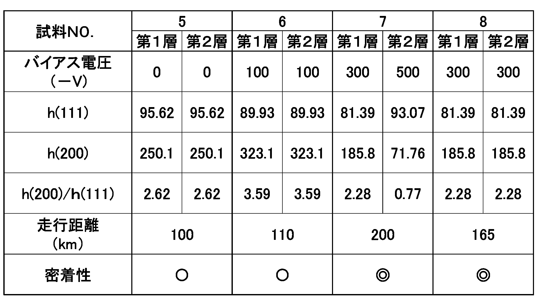
試料No.5~8のサーマルヘッドを搭載したサーマルプリンタは、走行距離が100kmを超え、保護層225の耐摩耗性が向上したことを確認できた。また、密着性の評価も◎または○となっており、保護層225の密着性が向上したことを確認できた。
Sample No. It was confirmed that the thermal printer equipped with the thermal heads of 5 to 8 had a travel distance exceeding 100 km and the wear resistance of the protective layer 225 was improved. In addition, the evaluation of adhesion was ◎ or ○, and it was confirmed that the adhesion of the protective layer 225 was improved.
また、第1層225aがP2>P1であり、第2層225bがP1>P2である試料No.7は、走行距離が200km以上あり、保護層225の耐摩耗性が向上するとともに、密着性が◎となっており、保護層225の密着性が向上したことを確認できた。
Sample No. 1 in which the first layer 225a is P2> P1 and the second layer 225b is P1> P2. No. 7 has a travel distance of 200 km or more, and the wear resistance of the protective layer 225 is improved and the adhesion is ◎, and it was confirmed that the adhesion of the protective layer 225 was improved.
また、試料No.7は、第2層225bのP2/P1が、第1層225aのP2/P1よりも小さくなっており、保護層225のすべり性が向上し、走行距離が200km以上あった。
Sample No. In No. 7, P2 / P1 of the second layer 225b was smaller than P2 / P1 of the first layer 225a, the slipperiness of the protective layer 225 was improved, and the traveling distance was 200 km or more.
また、試料No.8は、密着性が◎となっており、保護層225の密着性が向上したことを確認できた。
Sample No. In No. 8, the adhesion was ◎, and it was confirmed that the adhesion of the protective layer 225 was improved.
共通電極17、個別電極19、第1接続電極21および第2接続電極26等の各種電極配線が形成された試料となる基板を複数準備し、アークプラズマ方式イオンプレーティング装置を用いて、保護層225の成膜時において、600Vの基板バイアス電圧を印加して第1層225aを成膜し、表2に示す基板バイアス電圧を印加して、第2層225bを成膜した。第1層225aの厚みは2.5μmとした。第2層225bの厚みは2.5μmとした。
A plurality of substrates serving as samples on which various electrode wirings such as the common electrode 17, the individual electrode 19, the first connection electrode 21, and the second connection electrode 26 are formed, and a protective layer is formed using an arc plasma type ion plating apparatus. During the film formation of 225, a substrate bias voltage of 600 V was applied to form a first layer 225a, and a substrate bias voltage shown in Table 2 was applied to form a second layer 225b. The thickness of the first layer 225a was 2.5 μm. The thickness of the second layer 225b was 2.5 μm.
そして、実施例1と同様の走行試験を行い、保護層225の耐摩耗性を確認した。また、スティッキングの有無の確認を行った。
And the running test similar to Example 1 was done and the abrasion resistance of the protective layer 225 was confirmed. Also, the presence or absence of sticking was confirmed.
また、密着性を確認するために、R=0.2mm、120°のダイヤモンド圧子を備えるレスカ製CSR-1000のスクラッチ試験機を用いて、スクラッチ試験を行った。
In order to confirm the adhesion, a scratch test was performed using a Resca CSR-1000 scratch tester equipped with a diamond indenter of R = 0.2 mm and 120 °.
また、基板7の厚み方向に基板7を切断し、保護層25の断面出しを行い、X線のピーク強度を測定した。そのため、表3に記載されたX線強度比は、保護層225全体のX線強度比を示すものである。
Further, the substrate 7 was cut in the thickness direction of the substrate 7, the cross section of the protective layer 25 was taken out, and the peak intensity of the X-ray was measured. Therefore, the X-ray intensity ratio shown in Table 3 indicates the X-ray intensity ratio of the entire protective layer 225.
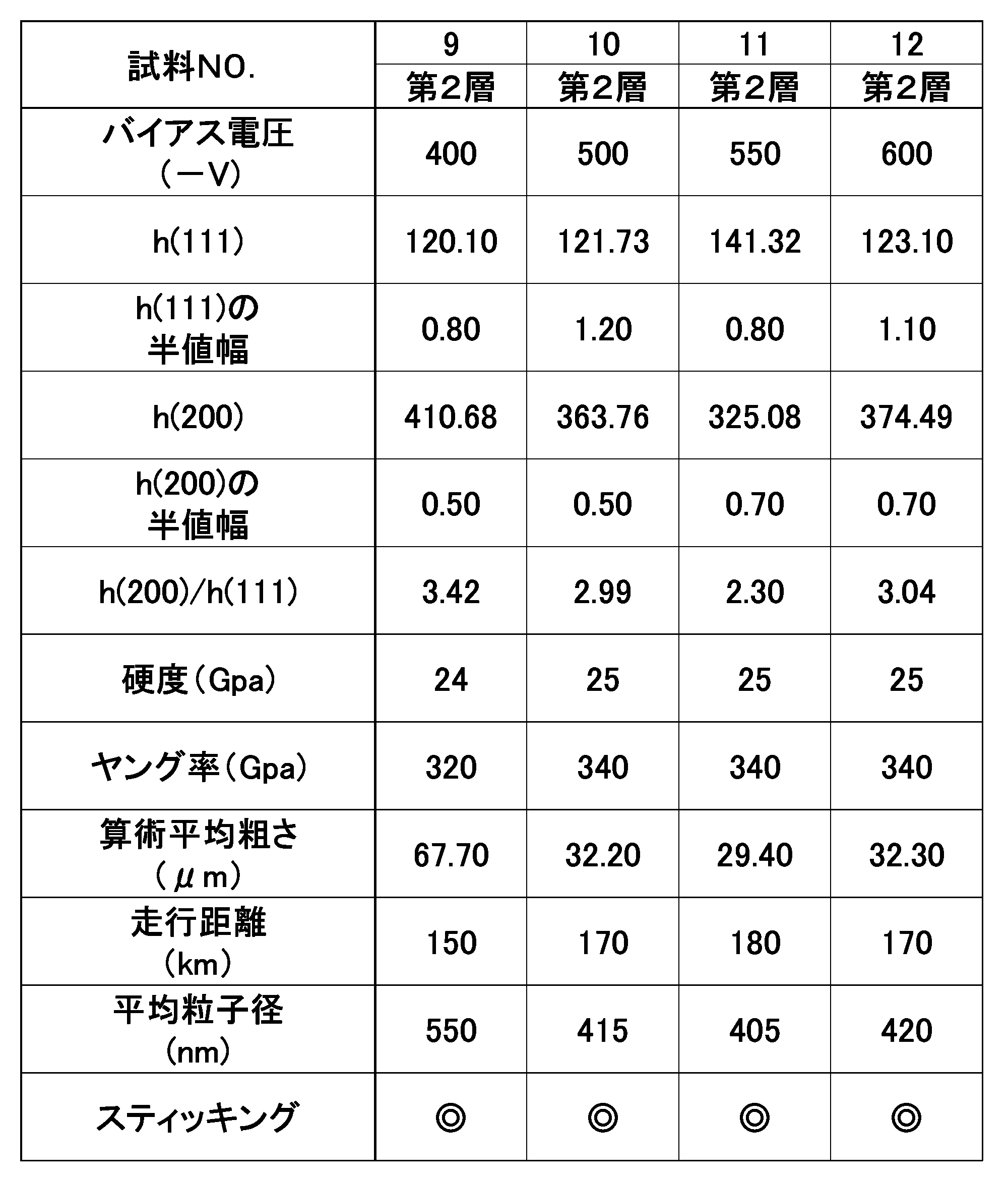
試料No.9~12のサーマルヘッドを搭載したサーマルプリンタは、走行距離が150kmを超え、保護層225の耐摩耗性が向上したことを確認できた。また、いずれもスティッキングの評価が◎となっていた。
Sample No. It was confirmed that the thermal printer equipped with the thermal heads 9 to 12 had a travel distance exceeding 150 km and the wear resistance of the protective layer 225 was improved. In all cases, the evaluation of sticking was ◎.
また、スクラッチ試験の結果も、試料No.9~12のサーマルヘッドは、密着強度が2.5kgf以上あり、保護層225の密着性が向上したことを確認した。
Also, the result of the scratch test is the sample No. The thermal heads 9 to 12 had an adhesion strength of 2.5 kgf or more, and it was confirmed that the adhesion of the protective layer 225 was improved.
また、P2/P1≦3.42となっている試料No.9~12は、走行試験の結果が150kmを超え、保護層225の耐摩耗性が向上したことを確認できた。
In addition, the sample No. satisfying P2 / P1 ≦ 3.42. For Nos. 9 to 12, it was confirmed that the result of the running test exceeded 150 km and the wear resistance of the protective layer 225 was improved.
また、(200)面の回折ピークの半値幅が、0.5°~0.7°である試料No.9~12は、走行試験の結果が150kmを超え、保護層225の耐摩耗性が向上したことを確認できた。
Specimen No. whose diffraction peak on the (200) plane has a half width of 0.5 ° to 0.7 °. For Nos. 9 to 12, it was confirmed that the result of the running test exceeded 150 km and the wear resistance of the protective layer 225 was improved.
また、(111)面の回折ピークの半値幅が、0.8°~1.2°である試料No.9~12は、走行試験の結果が150kmを超え、保護層225の耐摩耗性が向上したことを確認できた。
Specimen No. whose half-width of diffraction peak on (111) plane is 0.8 ° to 1.2 °. For Nos. 9 to 12, it was confirmed that the result of the running test exceeded 150 km and the wear resistance of the protective layer 225 was improved.
また、保護層25の硬度が24GPa以上ある試料No.9~12は、走行試験の結果が150kmを超え、保護層225の耐摩耗性が向上したことを確認できた。
Specimen No. in which the hardness of the protective layer 25 is 24 GPa or more. For Nos. 9 to 12, it was confirmed that the result of the running test exceeded 150 km and the wear resistance of the protective layer 225 was improved.
また、保護層25のヤング率が320GPa以上ある試料No.9~12は、走行試験の結果が150kmを超え、保護層225の耐摩耗性が向上したことを確認できた。
In addition, sample No. with a Young's modulus of the protective layer 25 of 320 GPa or more. For Nos. 9 to 12, it was confirmed that the result of the running test exceeded 150 km and the wear resistance of the protective layer 225 was improved.
また、保護層25の算術表面粗さRaが、67.7nm以下である試料No.9~12は、走行試験の結果が150kmを超え、保護層225の耐摩耗性が向上したことを確認できた。
In addition, Sample No. with an arithmetic surface roughness Ra of the protective layer 25 of 67.7 nm or less. For Nos. 9 to 12, it was confirmed that the result of the running test exceeded 150 km and the wear resistance of the protective layer 225 was improved.
特に、保護層25の算術表面粗さRaが、32.3nm以下である試料No.10~12は、走行試験の結果が170kmを超えていた。
In particular, Sample No. in which the protective surface 25 has an arithmetic surface roughness Ra of 32.3 nm or less. For 10-12, the results of the running test exceeded 170 km.
また、保護層25を構成する結晶粒子の平均結晶粒径が、405nm~550nmである試料No.9~12は、走行試験の結果が150kmを超え、保護層225の耐摩耗性が向上したことを確認できた。
In addition, the sample No. 1 in which the average crystal grain size of the crystal grains constituting the protective layer 25 is 405 nm to 550 nm. For Nos. 9 to 12, it was confirmed that the result of the running test exceeded 150 km and the wear resistance of the protective layer 225 was improved.
X1 サーマルヘッド
Z1 サーマルプリンタ
1 放熱板
3 ヘッド基体
7 基板
9 発熱部
11 駆動IC
12 封止部材
13 蓄熱層
14 接着部材
15 電気抵抗層
17 共通電極
19 個別電極
21 第1接続電極
25,225 保護層 225a 第1層
225b 第2層
26 第2接続電極
27 被覆層
31 コネクタ X1 Thermal head Z1Thermal printer 1 Heat sink 3 Head base 7 Substrate 9 Heating part 11 Drive IC
DESCRIPTION OFSYMBOLS 12 Sealing member 13 Heat storage layer 14 Adhesive member 15 Electrical resistance layer 17 Common electrode 19 Individual electrode 21 1st connection electrode 25,225 Protection layer 225a 1st layer 225b 2nd layer 26 2nd connection electrode 27 Covering layer 31 Connector
Z1 サーマルプリンタ
1 放熱板
3 ヘッド基体
7 基板
9 発熱部
11 駆動IC
12 封止部材
13 蓄熱層
14 接着部材
15 電気抵抗層
17 共通電極
19 個別電極
21 第1接続電極
25,225 保護層 225a 第1層
225b 第2層
26 第2接続電極
27 被覆層
31 コネクタ X1 Thermal head Z1
DESCRIPTION OF
Claims (14)
- 基板と、
前記基板上に位置する発熱部と、
前記基板上に位置し、前記発熱部に繋がっている電極と、
前記発熱部および前記電極の一部を被覆する保護層と、を備え、
前記保護層は、チタンおよび窒素を含んでおり、
前記保護層は、(111)面のX線回折のピーク強度をP1、(200)面のX線回折のピーク強度をP2とした場合に、
P2>P1である、サーマルヘッド。 A substrate,
A heat generating part located on the substrate;
An electrode located on the substrate and connected to the heat generating part;
A protective layer covering a part of the heat generating part and the electrode,
The protective layer contains titanium and nitrogen;
When the peak intensity of (111) plane X-ray diffraction is P1, and the peak intensity of (200) plane X-ray diffraction is P2,
A thermal head in which P2> P1. - 4.74≧(P2/P1)である、請求項1に記載のサーマルヘッド。 4. The thermal head according to claim 1, wherein 4.74 ≧ (P2 / P1).
- 前記保護層は、X線回折によって測定される(200)面の回折ピークの半値幅が0.5°~1°の範囲にある、請求項1または2に記載のサーマルヘッド。 3. The thermal head according to claim 1, wherein the protective layer has a half-value width of a diffraction peak of a (200) plane measured by X-ray diffraction in a range of 0.5 ° to 1 °.
- 前記保護層は、X線回折によって測定される(111)面の回折ピークの半値幅が0.0.8°~1.2°の範囲にある、請求項1から3のいずれか1項に記載のサーマルヘッド。 The protective layer according to any one of claims 1 to 3, wherein a half width of a diffraction peak of a (111) plane measured by X-ray diffraction is in a range of 0.00.8 ° to 1.2 °. The thermal head described.
- 前記保護層は、硬度が24GPa以上である、請求項1から4のいずれか一項に記載のサーマルヘッド。 The thermal head according to any one of claims 1 to 4, wherein the protective layer has a hardness of 24 GPa or more.
- 前記保護層は、ヤング率が320GPa以上である、請求項1から5のいずれか一項に記載のサーマルヘッド。 The thermal head according to any one of claims 1 to 5, wherein the protective layer has a Young's modulus of 320 GPa or more.
- 前記保護層の表面における算術表面粗さをRaとしたとき、67.7nm≧Raである、請求項1から6のいずれか一項に記載のサーマルヘッド。 The thermal head according to any one of claims 1 to 6, wherein 67.7 nm ≧ Ra, where Ra is an arithmetic surface roughness on the surface of the protective layer.
- 前記保護層を構成する結晶粒子が、前記基板の厚み方向に長い柱状粒子を含む、請求項1から7までのいずれか一項に記載のサーマルヘッド。 The thermal head according to any one of claims 1 to 7, wherein the crystal particles constituting the protective layer include columnar particles that are long in the thickness direction of the substrate.
- 前記保護層を構成する結晶粒子の平均結晶粒径が、205nm~605nmである、請求項1から8のいずれか一項に記載のサーマルヘッド。 The thermal head according to any one of claims 1 to 8, wherein an average crystal grain size of crystal grains constituting the protective layer is 205 nm to 605 nm.
- 前記平均結晶粒径の標準偏差が、16.7nm~60.8nmである、請求項9に記載のサーマルヘッド。 The thermal head according to claim 9, wherein a standard deviation of the average crystal grain size is 16.7 nm to 60.8 nm.
- 前記保護層は、第1層と前記第1層上に位置する第2層とを備え、
前記第1層は、P2>P1である、請求項1から10のいずれか一項に記載のサーマルヘッド。 The protective layer includes a first layer and a second layer located on the first layer,
The thermal head according to any one of claims 1 to 10, wherein the first layer satisfies P2> P1. - 前記第2層は、P1>P2である、請求項11に記載のサーマルヘッド。 The thermal head according to claim 11, wherein the second layer satisfies P1> P2.
- 前記第2層のP2/P1が、前記第1層のP2/P1よりも小さい、請求項11または12に記載のサーマルヘッド。 The thermal head according to claim 11 or 12, wherein P2 / P1 of the second layer is smaller than P2 / P1 of the first layer.
- 請求項1から13のうちいずれか一項に記載のサーマルヘッドと、
前記発熱部上を通過するように記録媒体を搬送する搬送機構と、
前記記録媒体を押圧するプラテンローラと、を備えることを特徴とするサーマルプリンタ。 The thermal head according to any one of claims 1 to 13,
A transport mechanism for transporting a recording medium so as to pass over the heat generating unit;
A thermal printer comprising: a platen roller that presses the recording medium.
Priority Applications (4)
| Application Number | Priority Date | Filing Date | Title |
|---|---|---|---|
| JP2018541228A JP6419404B1 (en) | 2017-03-29 | 2018-03-23 | Thermal head and thermal printer |
| US16/498,066 US10882329B2 (en) | 2017-03-29 | 2018-03-23 | Thermal head and thermal printer |
| CN201880021712.8A CN110461615B (en) | 2017-03-29 | 2018-03-23 | Thermal head and thermal printer |
| EP18777043.3A EP3608113B1 (en) | 2017-03-29 | 2018-03-23 | Thermal head and thermal printer |
Applications Claiming Priority (4)
| Application Number | Priority Date | Filing Date | Title |
|---|---|---|---|
| JP2017065424 | 2017-03-29 | ||
| JP2017-065424 | 2017-03-29 | ||
| JP2017208288 | 2017-10-27 | ||
| JP2017-208288 | 2017-10-27 |
Publications (1)
| Publication Number | Publication Date |
|---|---|
| WO2018181025A1 true WO2018181025A1 (en) | 2018-10-04 |
Family
ID=63675713
Family Applications (1)
| Application Number | Title | Priority Date | Filing Date |
|---|---|---|---|
| PCT/JP2018/011787 WO2018181025A1 (en) | 2017-03-29 | 2018-03-23 | Thermal head and thermal printer |
Country Status (5)
| Country | Link |
|---|---|
| US (1) | US10882329B2 (en) |
| EP (1) | EP3608113B1 (en) |
| JP (2) | JP6419404B1 (en) |
| CN (1) | CN110461615B (en) |
| WO (1) | WO2018181025A1 (en) |
Families Citing this family (1)
| Publication number | Priority date | Publication date | Assignee | Title |
|---|---|---|---|---|
| JP2021172028A (en) * | 2020-04-27 | 2021-11-01 | ローム株式会社 | Thermal print head, manufacturing method of thermal print head, and thermal printer |
Citations (11)
| Publication number | Priority date | Publication date | Assignee | Title |
|---|---|---|---|---|
| JPS623738U (en) | 1985-06-21 | 1987-01-10 | ||
| US5745147A (en) * | 1995-07-13 | 1998-04-28 | Eastman Kodak Company | Resistance-stable thermal print heads |
| JPH11124665A (en) * | 1997-10-17 | 1999-05-11 | Nippon Pillar Packing Co Ltd | Frictional sliding member and its manufacture |
| JP2009032855A (en) * | 2007-07-26 | 2009-02-12 | Panasonic Corp | Yield prediction method and yield prediction system |
| WO2009025112A1 (en) * | 2007-08-22 | 2009-02-26 | Sumitomo Electric Industries, Ltd. | Surface-coated cutting tool |
| JP2009126117A (en) * | 2007-11-27 | 2009-06-11 | Toshiba Hokuto Electronics Corp | Thermal print head, its manufacturing method and thermal printer |
| JP2010095800A (en) * | 2000-12-28 | 2010-04-30 | Kobe Steel Ltd | Method of producing hard film |
| JP2010149515A (en) * | 2008-11-26 | 2010-07-08 | Kyocera Corp | Recording head and recording device equipped therewith |
| WO2010125810A1 (en) * | 2009-04-28 | 2010-11-04 | キヤノンアネルバ株式会社 | Semiconductor device and method for fabricating same |
| JP2012104735A (en) * | 2010-11-12 | 2012-05-31 | Panasonic Corp | Semiconductor device and manufacturing method thereof |
| JP2016107396A (en) * | 2014-11-27 | 2016-06-20 | 三菱マテリアル株式会社 | Surface-coated cutting tool with excellent chipping resistance and wear resistance |
Family Cites Families (14)
| Publication number | Priority date | Publication date | Assignee | Title |
|---|---|---|---|---|
| US5374946A (en) | 1992-02-20 | 1994-12-20 | Alps Electric Co., Ltd. | Sliding contact part for recording medium |
| EP1698714B1 (en) | 2000-12-28 | 2009-09-02 | Kabushiki Kaisha Kobe Seiko Sho | Target used to form a hard film |
| JP2003095800A (en) * | 2001-09-27 | 2003-04-03 | Sumitomo Metal Ind Ltd | Crystallizing tip for organic polymer and crystal forming apparatus having the same |
| EP1564312B1 (en) * | 2004-02-12 | 2018-12-05 | Hitachi Tool Engineering Ltd. | Hard coating and its formation method, and hard-coated tool |
| JP2006231523A (en) | 2005-02-22 | 2006-09-07 | Toshiba Hokuto Electronics Corp | Thermal head |
| JP2008195046A (en) * | 2007-02-16 | 2008-08-28 | Toshiba Hokuto Electronics Corp | Thermal head |
| JP5311336B2 (en) * | 2008-11-28 | 2013-10-09 | セイコーインスツル株式会社 | Thermal head, thermal printer and thermal head manufacturing method |
| JP5995080B2 (en) * | 2012-12-20 | 2016-09-21 | 三菱マテリアル株式会社 | Surface coated cutting tool made of cubic boron nitride based ultra-high pressure sintered material with excellent crack resistance |
| US9511585B2 (en) * | 2013-07-12 | 2016-12-06 | Hewlett-Packard Development Company, L.P. | Thermal inkjet printhead stack with amorphous thin metal protective layer |
| CN103726014B (en) * | 2014-01-03 | 2016-07-20 | 中国科学院宁波材料技术与工程研究所 | A kind of VN wear-resistant coating of low wear rate and preparation method thereof |
| WO2016084939A1 (en) | 2014-11-27 | 2016-06-02 | 三菱マテリアル株式会社 | Surface-coated cutting tool with excellent chipping resistance and wear resistance |
| JP6590255B2 (en) | 2015-03-13 | 2019-10-16 | 三菱マテリアル株式会社 | Surface coated cutting tool with excellent chipping resistance due to hard coating layer |
| WO2016148056A1 (en) | 2015-03-13 | 2016-09-22 | 三菱マテリアル株式会社 | Surface-coated cutting tool with rigid coating layers exhibiting excellent chipping resistance |
| WO2017073681A1 (en) | 2015-10-29 | 2017-05-04 | 京セラ株式会社 | Thermal head and thermal printer |
-
2018
- 2018-03-23 US US16/498,066 patent/US10882329B2/en active Active
- 2018-03-23 EP EP18777043.3A patent/EP3608113B1/en active Active
- 2018-03-23 JP JP2018541228A patent/JP6419404B1/en active Active
- 2018-03-23 WO PCT/JP2018/011787 patent/WO2018181025A1/en unknown
- 2018-03-23 CN CN201880021712.8A patent/CN110461615B/en active Active
- 2018-10-01 JP JP2018186743A patent/JP2019069598A/en active Pending
Patent Citations (11)
| Publication number | Priority date | Publication date | Assignee | Title |
|---|---|---|---|---|
| JPS623738U (en) | 1985-06-21 | 1987-01-10 | ||
| US5745147A (en) * | 1995-07-13 | 1998-04-28 | Eastman Kodak Company | Resistance-stable thermal print heads |
| JPH11124665A (en) * | 1997-10-17 | 1999-05-11 | Nippon Pillar Packing Co Ltd | Frictional sliding member and its manufacture |
| JP2010095800A (en) * | 2000-12-28 | 2010-04-30 | Kobe Steel Ltd | Method of producing hard film |
| JP2009032855A (en) * | 2007-07-26 | 2009-02-12 | Panasonic Corp | Yield prediction method and yield prediction system |
| WO2009025112A1 (en) * | 2007-08-22 | 2009-02-26 | Sumitomo Electric Industries, Ltd. | Surface-coated cutting tool |
| JP2009126117A (en) * | 2007-11-27 | 2009-06-11 | Toshiba Hokuto Electronics Corp | Thermal print head, its manufacturing method and thermal printer |
| JP2010149515A (en) * | 2008-11-26 | 2010-07-08 | Kyocera Corp | Recording head and recording device equipped therewith |
| WO2010125810A1 (en) * | 2009-04-28 | 2010-11-04 | キヤノンアネルバ株式会社 | Semiconductor device and method for fabricating same |
| JP2012104735A (en) * | 2010-11-12 | 2012-05-31 | Panasonic Corp | Semiconductor device and manufacturing method thereof |
| JP2016107396A (en) * | 2014-11-27 | 2016-06-20 | 三菱マテリアル株式会社 | Surface-coated cutting tool with excellent chipping resistance and wear resistance |
Non-Patent Citations (1)
| Title |
|---|
| See also references of EP3608113A4 |
Also Published As
| Publication number | Publication date |
|---|---|
| CN110461615A (en) | 2019-11-15 |
| EP3608113A1 (en) | 2020-02-12 |
| JP2019069598A (en) | 2019-05-09 |
| JP6419404B1 (en) | 2018-11-07 |
| JPWO2018181025A1 (en) | 2019-04-04 |
| EP3608113B1 (en) | 2022-11-30 |
| US20200101761A1 (en) | 2020-04-02 |
| CN110461615B (en) | 2021-03-05 |
| EP3608113A4 (en) | 2020-12-16 |
| US10882329B2 (en) | 2021-01-05 |
Similar Documents
| Publication | Publication Date | Title |
|---|---|---|
| WO2013080915A1 (en) | Thermal head and thermal printer provided with same | |
| JP2016164005A (en) | Thermal head and thermal printer including the same | |
| JP5918383B2 (en) | Thermal head and thermal printer equipped with the same | |
| JP6196417B1 (en) | Thermal head and thermal printer | |
| JP6431200B2 (en) | Thermal head and thermal printer | |
| JP6419404B1 (en) | Thermal head and thermal printer | |
| JP2012030439A (en) | Thermal head and thermal printer including the same | |
| JP6258783B2 (en) | Thermal head and thermal printer equipped with the same | |
| JP5944636B2 (en) | Thermal head and thermal printer equipped with the same | |
| CN115315356A (en) | Thermal head and thermal printer | |
| JP6818939B2 (en) | Thermal head and thermal printer | |
| JP6849551B2 (en) | Thermal head and thermal printer | |
| JP7036692B2 (en) | Thermal head and thermal printer | |
| JP6773596B2 (en) | Thermal head and thermal printer | |
| JP6901419B2 (en) | Thermal head and thermal printer | |
| JP2018034371A (en) | Thermal head and thermal printer | |
| WO2020067424A1 (en) | Thermal head and thermal printer | |
| WO2021200869A1 (en) | Thermal head and thermal printer | |
| JP6426541B2 (en) | Thermal head and thermal printer | |
| JP6725402B2 (en) | Thermal head and thermal printer |
Legal Events
| Date | Code | Title | Description |
|---|---|---|---|
| ENP | Entry into the national phase |
Ref document number: 2018541228 Country of ref document: JP Kind code of ref document: A |
|
| 121 | Ep: the epo has been informed by wipo that ep was designated in this application |
Ref document number: 18777043 Country of ref document: EP Kind code of ref document: A1 |
|
| NENP | Non-entry into the national phase |
Ref country code: DE |
|
| ENP | Entry into the national phase |
Ref document number: 2018777043 Country of ref document: EP Effective date: 20191029 |