WO2018174076A1 - 光束制御部材、発光装置および面光源装置 - Google Patents
光束制御部材、発光装置および面光源装置 Download PDFInfo
- Publication number
- WO2018174076A1 WO2018174076A1 PCT/JP2018/011134 JP2018011134W WO2018174076A1 WO 2018174076 A1 WO2018174076 A1 WO 2018174076A1 JP 2018011134 W JP2018011134 W JP 2018011134W WO 2018174076 A1 WO2018174076 A1 WO 2018174076A1
- Authority
- WO
- WIPO (PCT)
- Prior art keywords
- light
- incident
- light emitting
- incident surface
- axis
- Prior art date
- Legal status (The legal status is an assumption and is not a legal conclusion. Google has not performed a legal analysis and makes no representation as to the accuracy of the status listed.)
- Ceased
Links
Images




Classifications
-
- G—PHYSICS
- G02—OPTICS
- G02F—OPTICAL DEVICES OR ARRANGEMENTS FOR THE CONTROL OF LIGHT BY MODIFICATION OF THE OPTICAL PROPERTIES OF THE MEDIA OF THE ELEMENTS INVOLVED THEREIN; NON-LINEAR OPTICS; FREQUENCY-CHANGING OF LIGHT; OPTICAL LOGIC ELEMENTS; OPTICAL ANALOGUE/DIGITAL CONVERTERS
- G02F1/00—Devices or arrangements for the control of the intensity, colour, phase, polarisation or direction of light arriving from an independent light source, e.g. switching, gating or modulating; Non-linear optics
- G02F1/01—Devices or arrangements for the control of the intensity, colour, phase, polarisation or direction of light arriving from an independent light source, e.g. switching, gating or modulating; Non-linear optics for the control of the intensity, phase, polarisation or colour
- G02F1/13—Devices or arrangements for the control of the intensity, colour, phase, polarisation or direction of light arriving from an independent light source, e.g. switching, gating or modulating; Non-linear optics for the control of the intensity, phase, polarisation or colour based on liquid crystals, e.g. single liquid crystal display cells
- G02F1/133—Constructional arrangements; Operation of liquid crystal cells; Circuit arrangements
- G02F1/1333—Constructional arrangements; Manufacturing methods
- G02F1/1335—Structural association of cells with optical devices, e.g. polarisers or reflectors
- G02F1/1336—Illuminating devices
- G02F1/133602—Direct backlight
- G02F1/133603—Direct backlight with LEDs
-
- G—PHYSICS
- G09—EDUCATION; CRYPTOGRAPHY; DISPLAY; ADVERTISING; SEALS
- G09G—ARRANGEMENTS OR CIRCUITS FOR CONTROL OF INDICATING DEVICES USING STATIC MEANS TO PRESENT VARIABLE INFORMATION
- G09G3/00—Control arrangements or circuits, of interest only in connection with visual indicators other than cathode-ray tubes
- G09G3/20—Control arrangements or circuits, of interest only in connection with visual indicators other than cathode-ray tubes for presentation of an assembly of a number of characters, e.g. a page, by composing the assembly by combination of individual elements arranged in a matrix no fixed position being assigned to or needed to be assigned to the individual characters or partial characters
- G09G3/34—Control arrangements or circuits, of interest only in connection with visual indicators other than cathode-ray tubes for presentation of an assembly of a number of characters, e.g. a page, by composing the assembly by combination of individual elements arranged in a matrix no fixed position being assigned to or needed to be assigned to the individual characters or partial characters by control of light from an independent source
- G09G3/3406—Control of illumination source
- G09G3/3413—Details of control of colour illumination sources
-
- G—PHYSICS
- G02—OPTICS
- G02F—OPTICAL DEVICES OR ARRANGEMENTS FOR THE CONTROL OF LIGHT BY MODIFICATION OF THE OPTICAL PROPERTIES OF THE MEDIA OF THE ELEMENTS INVOLVED THEREIN; NON-LINEAR OPTICS; FREQUENCY-CHANGING OF LIGHT; OPTICAL LOGIC ELEMENTS; OPTICAL ANALOGUE/DIGITAL CONVERTERS
- G02F1/00—Devices or arrangements for the control of the intensity, colour, phase, polarisation or direction of light arriving from an independent light source, e.g. switching, gating or modulating; Non-linear optics
- G02F1/01—Devices or arrangements for the control of the intensity, colour, phase, polarisation or direction of light arriving from an independent light source, e.g. switching, gating or modulating; Non-linear optics for the control of the intensity, phase, polarisation or colour
- G02F1/13—Devices or arrangements for the control of the intensity, colour, phase, polarisation or direction of light arriving from an independent light source, e.g. switching, gating or modulating; Non-linear optics for the control of the intensity, phase, polarisation or colour based on liquid crystals, e.g. single liquid crystal display cells
- G02F1/133—Constructional arrangements; Operation of liquid crystal cells; Circuit arrangements
- G02F1/1333—Constructional arrangements; Manufacturing methods
- G02F1/1335—Structural association of cells with optical devices, e.g. polarisers or reflectors
- G02F1/1336—Illuminating devices
- G02F1/133602—Direct backlight
- G02F1/133605—Direct backlight including specially adapted reflectors
-
- G—PHYSICS
- G02—OPTICS
- G02F—OPTICAL DEVICES OR ARRANGEMENTS FOR THE CONTROL OF LIGHT BY MODIFICATION OF THE OPTICAL PROPERTIES OF THE MEDIA OF THE ELEMENTS INVOLVED THEREIN; NON-LINEAR OPTICS; FREQUENCY-CHANGING OF LIGHT; OPTICAL LOGIC ELEMENTS; OPTICAL ANALOGUE/DIGITAL CONVERTERS
- G02F1/00—Devices or arrangements for the control of the intensity, colour, phase, polarisation or direction of light arriving from an independent light source, e.g. switching, gating or modulating; Non-linear optics
- G02F1/01—Devices or arrangements for the control of the intensity, colour, phase, polarisation or direction of light arriving from an independent light source, e.g. switching, gating or modulating; Non-linear optics for the control of the intensity, phase, polarisation or colour
- G02F1/13—Devices or arrangements for the control of the intensity, colour, phase, polarisation or direction of light arriving from an independent light source, e.g. switching, gating or modulating; Non-linear optics for the control of the intensity, phase, polarisation or colour based on liquid crystals, e.g. single liquid crystal display cells
- G02F1/133—Constructional arrangements; Operation of liquid crystal cells; Circuit arrangements
- G02F1/1333—Constructional arrangements; Manufacturing methods
- G02F1/1335—Structural association of cells with optical devices, e.g. polarisers or reflectors
- G02F1/1336—Illuminating devices
- G02F1/133602—Direct backlight
- G02F1/133606—Direct backlight including a specially adapted diffusing, scattering or light controlling members
-
- G—PHYSICS
- G02—OPTICS
- G02F—OPTICAL DEVICES OR ARRANGEMENTS FOR THE CONTROL OF LIGHT BY MODIFICATION OF THE OPTICAL PROPERTIES OF THE MEDIA OF THE ELEMENTS INVOLVED THEREIN; NON-LINEAR OPTICS; FREQUENCY-CHANGING OF LIGHT; OPTICAL LOGIC ELEMENTS; OPTICAL ANALOGUE/DIGITAL CONVERTERS
- G02F1/00—Devices or arrangements for the control of the intensity, colour, phase, polarisation or direction of light arriving from an independent light source, e.g. switching, gating or modulating; Non-linear optics
- G02F1/01—Devices or arrangements for the control of the intensity, colour, phase, polarisation or direction of light arriving from an independent light source, e.g. switching, gating or modulating; Non-linear optics for the control of the intensity, phase, polarisation or colour
- G02F1/13—Devices or arrangements for the control of the intensity, colour, phase, polarisation or direction of light arriving from an independent light source, e.g. switching, gating or modulating; Non-linear optics for the control of the intensity, phase, polarisation or colour based on liquid crystals, e.g. single liquid crystal display cells
- G02F1/133—Constructional arrangements; Operation of liquid crystal cells; Circuit arrangements
- G02F1/1333—Constructional arrangements; Manufacturing methods
- G02F1/1335—Structural association of cells with optical devices, e.g. polarisers or reflectors
- G02F1/1336—Illuminating devices
- G02F1/133602—Direct backlight
- G02F1/133611—Direct backlight including means for improving the brightness uniformity
-
- G—PHYSICS
- G09—EDUCATION; CRYPTOGRAPHY; DISPLAY; ADVERTISING; SEALS
- G09G—ARRANGEMENTS OR CIRCUITS FOR CONTROL OF INDICATING DEVICES USING STATIC MEANS TO PRESENT VARIABLE INFORMATION
- G09G3/00—Control arrangements or circuits, of interest only in connection with visual indicators other than cathode-ray tubes
- G09G3/20—Control arrangements or circuits, of interest only in connection with visual indicators other than cathode-ray tubes for presentation of an assembly of a number of characters, e.g. a page, by composing the assembly by combination of individual elements arranged in a matrix no fixed position being assigned to or needed to be assigned to the individual characters or partial characters
- G09G3/34—Control arrangements or circuits, of interest only in connection with visual indicators other than cathode-ray tubes for presentation of an assembly of a number of characters, e.g. a page, by composing the assembly by combination of individual elements arranged in a matrix no fixed position being assigned to or needed to be assigned to the individual characters or partial characters by control of light from an independent source
- G09G3/3406—Control of illumination source
-
- G—PHYSICS
- G09—EDUCATION; CRYPTOGRAPHY; DISPLAY; ADVERTISING; SEALS
- G09G—ARRANGEMENTS OR CIRCUITS FOR CONTROL OF INDICATING DEVICES USING STATIC MEANS TO PRESENT VARIABLE INFORMATION
- G09G3/00—Control arrangements or circuits, of interest only in connection with visual indicators other than cathode-ray tubes
- G09G3/20—Control arrangements or circuits, of interest only in connection with visual indicators other than cathode-ray tubes for presentation of an assembly of a number of characters, e.g. a page, by composing the assembly by combination of individual elements arranged in a matrix no fixed position being assigned to or needed to be assigned to the individual characters or partial characters
- G09G3/34—Control arrangements or circuits, of interest only in connection with visual indicators other than cathode-ray tubes for presentation of an assembly of a number of characters, e.g. a page, by composing the assembly by combination of individual elements arranged in a matrix no fixed position being assigned to or needed to be assigned to the individual characters or partial characters by control of light from an independent source
- G09G3/3406—Control of illumination source
- G09G3/342—Control of illumination source using several illumination sources separately controlled corresponding to different display panel areas, e.g. along one dimension such as lines
-
- G—PHYSICS
- G09—EDUCATION; CRYPTOGRAPHY; DISPLAY; ADVERTISING; SEALS
- G09G—ARRANGEMENTS OR CIRCUITS FOR CONTROL OF INDICATING DEVICES USING STATIC MEANS TO PRESENT VARIABLE INFORMATION
- G09G3/00—Control arrangements or circuits, of interest only in connection with visual indicators other than cathode-ray tubes
- G09G3/20—Control arrangements or circuits, of interest only in connection with visual indicators other than cathode-ray tubes for presentation of an assembly of a number of characters, e.g. a page, by composing the assembly by combination of individual elements arranged in a matrix no fixed position being assigned to or needed to be assigned to the individual characters or partial characters
- G09G3/34—Control arrangements or circuits, of interest only in connection with visual indicators other than cathode-ray tubes for presentation of an assembly of a number of characters, e.g. a page, by composing the assembly by combination of individual elements arranged in a matrix no fixed position being assigned to or needed to be assigned to the individual characters or partial characters by control of light from an independent source
- G09G3/3406—Control of illumination source
- G09G3/342—Control of illumination source using several illumination sources separately controlled corresponding to different display panel areas, e.g. along one dimension such as lines
- G09G3/3426—Control of illumination source using several illumination sources separately controlled corresponding to different display panel areas, e.g. along one dimension such as lines the different display panel areas being distributed in two dimensions, e.g. matrix
-
- F—MECHANICAL ENGINEERING; LIGHTING; HEATING; WEAPONS; BLASTING
- F21—LIGHTING
- F21V—FUNCTIONAL FEATURES OR DETAILS OF LIGHTING DEVICES OR SYSTEMS THEREOF; STRUCTURAL COMBINATIONS OF LIGHTING DEVICES WITH OTHER ARTICLES, NOT OTHERWISE PROVIDED FOR
- F21V5/00—Refractors for light sources
- F21V5/04—Refractors for light sources of lens shape
-
- F—MECHANICAL ENGINEERING; LIGHTING; HEATING; WEAPONS; BLASTING
- F21—LIGHTING
- F21V—FUNCTIONAL FEATURES OR DETAILS OF LIGHTING DEVICES OR SYSTEMS THEREOF; STRUCTURAL COMBINATIONS OF LIGHTING DEVICES WITH OTHER ARTICLES, NOT OTHERWISE PROVIDED FOR
- F21V5/00—Refractors for light sources
- F21V5/04—Refractors for light sources of lens shape
- F21V5/046—Refractors for light sources of lens shape the lens having a rotationally symmetrical shape about an axis for transmitting light in a direction mainly perpendicular to this axis, e.g. ring or annular lens with light source disposed inside the ring
-
- F—MECHANICAL ENGINEERING; LIGHTING; HEATING; WEAPONS; BLASTING
- F21—LIGHTING
- F21V—FUNCTIONAL FEATURES OR DETAILS OF LIGHTING DEVICES OR SYSTEMS THEREOF; STRUCTURAL COMBINATIONS OF LIGHTING DEVICES WITH OTHER ARTICLES, NOT OTHERWISE PROVIDED FOR
- F21V5/00—Refractors for light sources
- F21V5/08—Refractors for light sources producing an asymmetric light distribution
-
- G—PHYSICS
- G02—OPTICS
- G02F—OPTICAL DEVICES OR ARRANGEMENTS FOR THE CONTROL OF LIGHT BY MODIFICATION OF THE OPTICAL PROPERTIES OF THE MEDIA OF THE ELEMENTS INVOLVED THEREIN; NON-LINEAR OPTICS; FREQUENCY-CHANGING OF LIGHT; OPTICAL LOGIC ELEMENTS; OPTICAL ANALOGUE/DIGITAL CONVERTERS
- G02F1/00—Devices or arrangements for the control of the intensity, colour, phase, polarisation or direction of light arriving from an independent light source, e.g. switching, gating or modulating; Non-linear optics
- G02F1/01—Devices or arrangements for the control of the intensity, colour, phase, polarisation or direction of light arriving from an independent light source, e.g. switching, gating or modulating; Non-linear optics for the control of the intensity, phase, polarisation or colour
- G02F1/13—Devices or arrangements for the control of the intensity, colour, phase, polarisation or direction of light arriving from an independent light source, e.g. switching, gating or modulating; Non-linear optics for the control of the intensity, phase, polarisation or colour based on liquid crystals, e.g. single liquid crystal display cells
- G02F1/133—Constructional arrangements; Operation of liquid crystal cells; Circuit arrangements
- G02F1/1333—Constructional arrangements; Manufacturing methods
- G02F1/1335—Structural association of cells with optical devices, e.g. polarisers or reflectors
- G02F1/1336—Illuminating devices
- G02F1/133602—Direct backlight
- G02F1/133606—Direct backlight including a specially adapted diffusing, scattering or light controlling members
- G02F1/133607—Direct backlight including a specially adapted diffusing, scattering or light controlling members the light controlling member including light directing or refracting elements, e.g. prisms or lenses
Definitions
- the present invention relates to a light flux controlling member, a light emitting device, and a surface light source device.
- a direct type surface light source device may be used as a backlight.
- direct type surface light source devices having a plurality of light emitting elements as light sources have come to be used.
- a direct-type surface light source device has a substrate, a plurality of light emitting elements, a plurality of light flux control members (lenses), and a light diffusion member.
- the light emitting element is a light emitting diode (LED) such as a white light emitting diode.
- the plurality of light emitting elements are arranged in a matrix on the substrate (for example, a plurality of columns including the plurality of light emitting elements are arranged).
- a light flux controlling member that spreads light emitted from each light emitting element in the surface direction of the substrate is disposed on each light emitting element. The light emitted from the light flux controlling member is diffused by the light diffusing member and illuminates the irradiated member (for example, a liquid crystal panel) in a planar shape.
- Patent Document 1 As shown in FIGS. 1 and 2, a substrate 42, a plurality of LED modules (light emitting elements) 41, a plurality of lenses 45 (light flux controlling members), and a plurality of optical sheets (not shown). And a backlight unit 4 (surface light source device) having the same structure.
- the plurality of LED modules (light emitting elements) 41 and the plurality of lenses 45 (light flux controlling members) are arranged in a line at the center of the backlight unit 4.
- the lens 45 (light flux controlling member) has a light emitting surface 45a for emitting light emitted from the LED module 41 to the outside and a pair of side surfaces 45b sandwiching the light emitting surface 45a.
- the lens 45 causes the light emitted from the light emitting element to travel in the longitudinal direction of the lens 45 (the direction in which the light emitting surface 45a extends). Therefore, it is required to spread asymmetrically with respect to the optical axis of the light emitting element (to distribute the light in a biased direction).
- the lens 45 disclosed in Patent Document 1 is configured such that light emitted from a plurality of light emitting elements is symmetric with respect to the optical axis of the light emitting element in the longitudinal direction of the lens 45 (the direction in which the light emitting surface 45a extends). It spreads light. Therefore, when a row including a plurality of light emitting elements is arranged at a position deviated from the center of the surface light source device, there is a problem that light cannot sufficiently reach every corner of the surface light source device.
- a light flux controlling member is a light flux controlling member for controlling the light distribution of light emitted from a light emitting element, and in an XYZ coordinate system constituted by an X axis, a Y axis, and a Z axis perpendicular to each other, A first incidence plane that is parallel to the plane and extends in the Y-axis direction, and a part of the inner surface of the concave portion disposed on the rear side, and makes a part of the light emitted from the light emitting element incident.
- a third incident surface that allows a further part of the light emitted from the light emitting element to enter and reflects the light incident on the first incident surface, and in the Z-axis direction, Disposed on the front side opposite the back surface, and incident on the first incident surface;
- a first reflecting surface that reflects light incident on the first incident surface and reflected on the third incident surface and light incident on the third incident surface toward one side in the Y-axis direction, and on the front side
- a second reflection surface that is disposed and reflects light incident on the second incidence surface to the other side opposite to the one in the Y-axis direction, and sandwiches the first reflection surface and the second reflection surface It has a configuration including two emission surfaces that are arranged to face each other and emit light reflected by the first reflection surface or the second reflection surface to the outside.
- the light-emitting device includes a light-emitting element having an optical axis arranged in parallel with the Z-axis, and the first incident surface and the second incident surface arranged to face the light-emitting element. And a light flux controlling member according to the invention.
- the surface light source device employs a configuration having a plurality of light emitting devices according to the present invention and a light diffusing plate that diffuses and transmits the light emitted from the light emitting device.
- a light flux controlling member that can spread light emitted from the light emitting element asymmetrically with respect to the optical axis of the light emitting element in the longitudinal direction of the light flux controlling member.
- FIG. 1 is a diagram showing a configuration of a conventional surface light source device.
- FIG. 2 is a diagram showing a configuration of a conventional light flux controlling member.
- 3A and 3B are diagrams showing the configuration of the surface light source device according to the present embodiment.
- 4A and 4B are diagrams showing the configuration of the surface light source device according to the present embodiment.
- FIG. 5 is a partially enlarged cross-sectional view in which a part of FIG. 4B is enlarged.
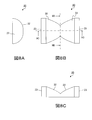
- 6A to 6C are diagrams showing the configuration of the light flux controlling member according to the present embodiment.
- 7A to 7C are diagrams showing the configuration of the light flux controlling member according to the present embodiment.
- 8A to 8C are diagrams showing the configuration of a comparative light flux controlling member.
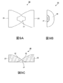
- FIGS. 9A to 9C are diagrams showing a configuration of a comparative light flux controlling member.
- 10A, 10B, and 10C are optical path diagrams in a comparative surface light source device using the light flux controlling member in FIGS.
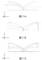
- 11A, 11B, and 11C are optical path diagrams in the surface light source device according to the present embodiment using the light flux controlling member in FIGS.
- FIG. 12 is a diagram showing an analysis result of the illuminance distribution on the light diffusing plate of the surface light source device using the comparative light flux controlling member.
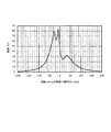
- FIG. 13 is a diagram showing an analysis result of the illuminance distribution on the light diffusion plate of the surface light source device using the light flux controlling member according to the present embodiment.
- FIG. 3 and 4 are diagrams showing the configuration of the surface light source device 100 according to the present embodiment.
- 3A is a plan view of the surface light source device 100
- FIG. 3B is a left side view.
- 4A is a plan view with the light diffusion plate 150 removed in FIG. 3A
- FIG. 4B is a cross-sectional view taken along line 4B-4B shown in FIG. 3A.
- FIG. 5 is a partially enlarged cross-sectional view in which a part of FIG. 4B is enlarged.
- the surface light source device 100 includes a housing 110, a substrate 120, a plurality of light emitting devices 130, and a light diffusing plate 150.
- the housing 110 is a box in which at least a part of one surface is opened to accommodate the substrate 120 and the plurality of light emitting devices 130 therein.
- the housing 110 includes a bottom plate 111 and a top plate 112 facing the bottom plate 111.
- the bottom plate 111 includes a horizontal portion 111a disposed in parallel with the top plate 112, and two inclined portions disposed so as to sandwich the horizontal portion 111a and inclined toward the top plate 112 (in one step or two steps or more).
- 111b and 111c The two inclined portions 111b and 111c reflect light emitted from the light emitting device 130 in a substantially horizontal direction toward the light diffusing plate 150 so that the light emitted from the light emitting device 130 can be easily collected on the light diffusing plate 150.
- the two inclined portions 111b and 111c have different inclination angles with respect to the horizontal portion 111a and lengths from the horizontal portion 111a to the top plate 112, and are provided asymmetrically (see FIG. 4B).
- the top plate 112 is formed with a rectangular opening serving as a light emitting region.
- the size of the opening corresponds to the size of the light emitting region formed in the light diffusion plate 150, and is, for example, 400 mm ⁇ 700 mm (32 inches). This opening is closed by the light diffusing plate 150.
- the height (space thickness) from the surface of the bottom plate 111a to the light diffusion plate 150 is not particularly limited, but is about 10 to 40 mm.
- the housing 110 is made of, for example, a resin such as polymethyl methacrylate (PMMA) or polycarbonate (PC), or a metal such as stainless steel or aluminum.
- the substrate 120 is a flat plate for disposing a plurality of light emitting devices 130 arranged on the bottom plate 111 of the housing 110 in the housing 110 at a predetermined interval.
- the surface of the substrate 120 is configured to reflect the light reaching from the light emitting device 130 toward the light diffusion plate 150.
- the plurality of light emitting devices 130 are arranged in a row on the substrate 120 and at a position shifted from the center of the bottom plate 111 when the surface light source device 100 is viewed in plan. Specifically, when the surface light source device 100 is viewed in plan, the row formed by the plurality of light emitting devices 130 is a pair of opposing sides of the light diffusion plate 150 (a pair of opposing long sides 150a and 150b in FIG. 3A). And the distance between one of a pair of opposite sides of the light diffusion plate 150 (long side 150a in FIG. 3A) is equal to the other of the pair of opposite sides of the light diffusion plate 150 (long side in FIG. 3A). 150b) and longer than the distance.
- the number of the light emitting devices 130 arranged on the substrate 120 is not particularly limited.
- the number of the light emitting devices 130 arranged on the substrate 120 is appropriately set based on the size of the light emitting area (light emitting surface) defined by the opening of the housing 110.
- Each of the plurality of light emitting devices 130 includes a light emitting element 131 and a light flux controlling member 132.
- the plurality of light emitting devices 130 are arranged such that the optical axes of light emitted from the light emitting elements 131 (optical axes LA of the light emitting elements 131 described later) are along the normal to the surface of the substrate 120.
- a first incident surface 133 (to be described later) of the light flux controlling member 132 has one of a pair of sides facing the light diffusion plate 150 (which is longer in FIG. 3A) than a second incident surface 134 to be described later. It is arranged so as to be close to the side 150a).
- the light emitting element 131 is a light source of the surface light source device 100 (and the light emitting device 130).
- the light emitting element 131 is disposed on the substrate 120.
- the light emitting element 131 is, for example, a light emitting diode (LED).
- the color of the emitted light of the light emitting element 131 included in the light emitting device 130 is not particularly limited.
- the light flux controlling member 132 controls the light distribution of the light emitted from the light emitting element 131, and the traveling direction of the light is substantially perpendicular to the optical axis LA of the light emitting element 131 and substantially opposite to each other. The direction is changed to two directions (directions corresponding to the positive and negative of the Y-axis described later).
- the light flux controlling member 132 is disposed on the light emitting element 131 so that its center axis CA is preferably coincident with the optical axis LA of the light emitting element 131 (see FIG. 5).
- the “optical axis LA of the light emitting element” means a light beam at the center of the three-dimensional outgoing light beam from the light emitting element 131.
- Center axis CA of light flux controlling member 12 means, for example, when light flux controlling member 12 is symmetrical twice except for first incident surface 133, second incident surface 134, third incident surface 135, and fourth incident surface 136. A symmetry axis that is two-fold symmetry.
- the central axis CA of the light flux controlling member is orthogonal to the Z axis and the Z axis, and the axes parallel to the direction in which the plurality of light emitting devices 130 are arranged are the X axis, the Z axis, and the X axis. Is also referred to as the Y-axis.
- the optical axis LA of the light emitting element 131 is arranged so as to be parallel to the Z axis and preferably coincide with the Z axis.
- the origin of the XYZ coordinate system can coincide with the light emission center of the light emitting element, for example.
- a virtual plane including the X axis and the Y axis is referred to as an XY plane
- a virtual plane including the Y axis and the Z axis is referred to as a YZ plane
- a virtual plane including the X axis and the Z axis is referred to as an XZ plane.
- the material of the light flux controlling member 132 is not particularly limited as long as it can transmit light having a desired wavelength.
- the material of the light flux controlling member 132 is light transmissive resin such as polymethyl methacrylate (PMMA), polycarbonate (PC), epoxy resin (EP), or glass.
- the surface light source device 100 has a main feature in the configuration of the light flux controlling member 132. Therefore, the light flux controlling member 132 will be described in detail separately.
- the light diffusion plate 150 is disposed so as to close the opening of the housing 110.
- light diffusing plate 150 has a rectangular shape corresponding to the shape of the opening of housing 110, and a pair of opposed long sides 150a and 150b, and a pair of opposed short sides 150c and 150d.
- the light diffusing plate 150 is a plate-like member having light transmission properties and light diffusing properties, and transmits the light emitted from the light emission surface 139 of the light flux controlling member 132 while diffusing it.
- the light diffusion plate 150 can be a light emitting surface of the surface light source device 100, for example.
- the material of the light diffusing plate 150 is not particularly limited as long as it can transmit the light emitted from the light exit surface 139 of the light flux controlling member 132 while diffusing it.
- PMMA polymethyl methacrylate
- PC polycarbonate
- PS polystyrene
- MS styrene / methyl methacrylate copolymer resin
- fine irregularities are formed on the surface of the light diffusion plate 150, or light diffusers such as beads are dispersed inside the light diffusion plate 150.
- the light emitted from each light emitting element 131 illuminates a wide range of the light diffusing plate 150 by the light flux controlling member 132, particularly with respect to the optical axis LA of the light emitting element 131.
- the light is changed into light that is directed in two directions (the Y-axis direction in FIG. 5) that are substantially vertical and substantially opposite to each other.
- the light emitted from each light flux controlling member 132 is further diffused by the light diffusion plate 150 and emitted to the outside.
- FIGS. 7A to 7C are diagrams showing the configuration of the light flux controlling member 132.
- FIG. 6A is a side view of the light flux controlling member 132
- FIG. 6B is a plan view
- FIG. 6C is a front view.
- 7A is a bottom view
- FIG. 7B is a sectional view taken along line 7B-7B in FIG. 6B
- FIG. 7C is a sectional view taken along line 7C-7C in FIG. 6B.
- the light flux controlling member 132 controls the light distribution of the light emitted from the light emitting element 131. As shown in FIGS. 6A to 6C, the light flux controlling member 132 includes a first incident surface 133, a second incident surface 134, a third incident surface 135, two fourth incident surfaces 136, a first reflecting surface 137, and a second reflecting surface. It has a reflection surface 138 and two emission surfaces 139.
- the first incident surface 133, the second incident surface 134, the third incident surface 135, and the fourth incident surface 136 are all formed at the center of the back surface 140 (the light emitting element 131 side, that is, the back surface) of the light flux controlling member 132. It is the inner surface of the recessed part 141 made.
- the back surface 140 is parallel to the XY plane and extends in the Y-axis direction.
- the first incident surface 133 is preferably disposed on one side with respect to the XZ plane, and allows a part of the light emitted from the light emitting element 131 to enter.
- the first incident surface 133 may be a flat surface or a curved surface.
- the first incident surface 133 is preferably substantially parallel to the XY plane from the viewpoint of increasing the light reflected by the third incident surface 135.
- substantially parallel to the XY plane means that the angle formed between the tangent plane at an arbitrary point on the first incident surface 133 and the XY plane is ⁇ 3 ° or less.
- the first incident surface 133 is a plane parallel to the XY plane.
- the second incident surface 134 is preferably disposed on the other side with respect to the XZ plane, and allows another part of the light emitted from the light emitting element 131 to enter.
- the second incident surface 134 preferably has a shape that allows light incident on the second incident surface to easily reach the second reflecting surface 134.
- the third incident surface 135 is disposed between the first incident surface 133 and the second incident surface 134, allows another part of the light emitted from the light emitting element 131 to enter, and the first incident surface 133. Reflects the incident light at.
- the third incident surface 135 may be a flat surface or a curved surface.
- the third incident surface 135 is preferably substantially parallel to the XZ plane from the viewpoint of increasing the amount of light that reflects the light incident on the first incident surface 133 toward the first reflecting surface 137.
- substantially parallel to the XZ plane means that the angle formed between the tangential plane at an arbitrary point on the third incident surface 135 and the XZ plane is ⁇ 3 ° or less.
- the third incident surface 135 is a plane on the XZ plane.
- the maximum depth of the recess 141 corresponding to the first incident surface 133 is preferably 0.1 to 0.5 times the maximum depth of the recess 141 corresponding to the second incident surface 134.
- the size of the third incident surface 135 is constant. It is easy to make the above, and it is easy to increase the amount of light incident on the first incident surface 133 and reflected on the third incident surface 135. Therefore, it is easy to spread light asymmetrically with respect to the optical axis LA.
- the maximum depth of the concave portion 141 corresponding to the first incident surface 133 represents the depth from the back surface 140 to the first incident surface 133, and the maximum depth of the concave portion 141 corresponding to the second incident surface 134.
- S represents the depth from the back surface 140 to the apex of the second incident surface 134 (the intersection of the Z axis and the second incident surface 134).
- the two fourth incident surfaces 136 are disposed between the first incident surface 133 and the back surface 140 and between the second incident surface 134 and the back surface 140, respectively. A part is incident.
- the first reflecting surface 137 is disposed on the side opposite to the light emitting element 131 (the light diffusing plate 150 side, that is, the front side) across the first incident surface 133.
- the first reflecting surface 137 includes light incident on the first incident surface 133, light incident on the first incident surface 133 and reflected on the third incident surface 135, and light incident on the third incident surface 135. Is reflected in one direction in the Y-axis direction.
- the second reflecting surface 138 is disposed on the opposite side (front side) of the light emitting element 131 with the second incident surface 134 interposed therebetween.
- the second reflecting surface 138 reflects the light incident on the second incident surface 134 to the other side opposite to the one in the Y-axis direction.
- the first reflection surface 137 and the second reflection surface 138 are each formed in a shape such that the first reflection surface 137 and the second reflection surface 138 move away from the Y axis as they move away from the Z axis. Specifically, in the first reflection surface 137 and the second reflection surface 138, in the cross section including the Z-axis and the Y-axis, the inclination of the tangent gradually decreases from the Z-axis toward the end (the emission surface 139). Each is formed so as to be along the Y axis.
- the two emission surfaces 139 are arranged so as to face each other with the first reflection surface 137 and the second reflection surface 138 interposed therebetween.
- the two exit surfaces 139 are incident on the first incident surface 133, the second incident surface 134, or the third incident surface 135, reflected by the first reflecting surface 137 or the second reflecting surface 138, and the fourth incident surface 136.
- the light that directly enters and reaches directly is emitted to the outside.
- FIGS. 8A to 9C are diagrams showing a configuration of a comparative light flux controlling member.
- 8A is a side view of the light flux controlling member 20 for comparison
- FIG. 8B is a plan view
- FIG. 8C is a front view.
- 9A is a bottom view
- FIG. 9B is a cross-sectional view taken along line 9B-9B in FIG. 8B
- FIG. 9C is a cross-sectional view taken along line 9C-9C in FIG. 8B.
- the light flux controlling member 20 for comparison has a light incident surface having a shape corresponding to the second light incident surface 134 instead of the first light incident surface 133 and the third light incident surface 135.
- the configuration is the same as that of the control member 132. That is, the comparative light flux controlling member 20 has a two-fold symmetrical shape not only on the reflecting surface 22 and the emitting surface 23 but also on the incident surface 21.
- the light path in the surface light source device 100 using the light flux controlling member according to the present embodiment (the light flux controlling member 132 in FIGS. 5 to 6C) and the illuminance distribution on the light diffusion plate 150 were analyzed.
- the analysis of the illuminance distribution on the optical path and the light diffusion plate 150 was performed using the surface light source device 100 having only one light emitting device 130.
- the optical path of the surface light source device using the comparative light beam control member (light beam control member 20 in FIGS. 8A to 9C) and the illuminance distribution on the light diffusion plate were also analyzed.
- (Parameter) -Outer diameter of light flux controlling member 20 mm length in the X-axis direction, 30 mm length in the Y-axis direction
- the maximum depth of the recess 141 corresponding to the first incident surface 133 is 0.4 mm.
- the maximum depth of the concave portion 141 corresponding to the second incident surface 134 is 2.1 mm.
- -Height of light emitting element 0.5mm -Size of light emitting element: ⁇ 2.6 mm -Distance between the substrate 120 and the light diffusion plate 150: 20 mm
- an angle inclined rightward with respect to the optical axis of off-axis light is represented by a positive sign, and an angle inclined leftward is represented by a negative sign. The same applies to the following.
- FIG. 12 is a diagram showing an analysis result of the illuminance distribution on the light diffusing plate 150 of the surface light source device using the comparative light flux controlling member.
- FIG. 13 is a diagram showing an analysis result of the illuminance distribution on the light diffusion plate 150 of the surface light source device 100 using the light flux controlling member according to the present embodiment.
- the horizontal axis of FIGS. 12 and 13 indicates the distance from the optical axis LA of the light emitting element 131 in the light diffusion plate 150 (distance in the Y-axis direction, mm), and the vertical axis indicates the illuminance at the light diffusion plate 150. Yes.
- the amount of light spreading on the positive side in the Y-axis direction is the same. Furthermore, as shown in FIG. 10C, the axial light emitted from the light emission center of the light emitting element 131 also spreads symmetrically with respect to the optical axis LA, and spreads on the negative side in the Y-axis direction, and in the Y-axis direction. It can be seen that the amount of light spreading to the positive side is the same.
- FIG. 11A in the surface light source device 100 using the light flux controlling member 132 according to the present embodiment, from the point on the positive side in the Y-axis direction with respect to the light emission center of the light emitting element 131. It can be seen that most of the emitted off-axis light is incident on the first incident surface 133 and the third incident surface 135, reflected by the first reflecting surface 137, and spreads to the negative side in the Y-axis direction.
- FIG. 11B a part of the off-axis light emitted from the point on the negative side in the Y-axis direction from the light emission center of the light emitting element 131 is incident on the second incident surface 134 and is second reflected.
- the optical path shown in FIG. 11A and the optical path shown in FIG. 11B are asymmetric with each other, and when the optical path shown in FIG. 11A and the optical path shown in FIG. 11B are added, the light spreading toward the negative side in the Y-axis direction is obtained. It can be seen that there is more light than the light spreading on the positive side in the Y-axis direction. Further, as shown in FIG. 11A and the optical path shown in FIG. 11B are asymmetric with each other, and when the optical path shown in FIG. 11A and the optical path shown in FIG. 11B are added, the light spreading toward the negative side in the Y-axis direction is obtained. It can be seen that there is more light than the light spreading on the positive side in the Y-axis direction. Further, as shown in FIG.
- the surface light source device 100 using the light flux controlling member according to the present embodiment is more negative in the Y-axis direction (the left side in FIGS. 10 and 11) than the surface light source device using the comparative light flux controlling member. ), It is possible to spread more light than the positive side in the Y-axis direction (the right side in FIGS. 10 and 11), so that it is possible to spread the light asymmetrically with respect to the optical axis LA.
- the surface light source device using the comparative light flux controlling member has an illuminance distribution that is symmetric with respect to the optical axis LA.
- the illuminance on the negative side in the Y-axis direction is higher than the illuminance on the positive side in the Y-axis direction. It can be seen that the illuminance distribution is asymmetric with respect to the optical axis LA.
- the light flux controlling member 132 has the first incident surface 133 and the third incident surface 135.
- the off-axis light emitted from the point on the side where the light is desired to be spread with respect to the light emission center toward the side where the light is not desired to be spread is changed to the first incident surface.
- After making it enter in 133 it can reflect in the direction which wants to spread light by reflecting in the 3rd entrance plane 135 (contrast of FIG. 10B and 11B). In this way, in the Y-axis direction, more light can be spread on one side with respect to the optical axis LA than on the other side, so that light can be spread asymmetrically with respect to the optical axis LA.
- the light flux controlling member 132 is arranged such that the first incident surface 133 is closer to the long side 150a of the light diffusion plate 150 than the second incident surface 134 (FIG. 3A, 4A), even if the row formed by the plurality of light emitting devices 130 is arranged at a position shifted from the center of the bottom plate 111, light can reach every corner of the surface light source device 100.
- the case 110 is an example of a box composed of a bottom plate 111a and two inclined surfaces 111b sandwiching the bottom plate 111a.
- the present invention is not limited to this. It may be a rectangular parallelepiped box composed of an opposing top plate and four side plates that connect the bottom plate and the top plate.
- a reflecting plate having an inclined surface may be disposed inside the rectangular parallelepiped box.
- the present invention is not limited to this, and the light emitting devices 130 may be arranged in two or more rows.
- the light flux controlling member 132 does not have a leg portion is shown, but the present invention is not limited to this, and the leg portion may have a leg portion.
- the light flux controlling member 132 may have a plurality of substantially columnar legs protruding from the back surface 140 to the back side on the outer peripheral portion of the back surface 140.
- the light beam control member 132 has two fourth incident surfaces 136.
- the present invention is not limited to this.
- the light beam control member 132 has a plurality of legs on the outer periphery of the back surface 140. In the case of having a portion, the fourth incident surface 136 may not be provided.
- the surface light source device having the light flux controlling member according to the present invention can be applied to, for example, a backlight of a liquid crystal display device, a signboard, or general illumination.
Landscapes
- Physics & Mathematics (AREA)
- Nonlinear Science (AREA)
- General Physics & Mathematics (AREA)
- Engineering & Computer Science (AREA)
- Chemical & Material Sciences (AREA)
- Mathematical Physics (AREA)
- Crystallography & Structural Chemistry (AREA)
- Optics & Photonics (AREA)
- Theoretical Computer Science (AREA)
- Computer Hardware Design (AREA)
- Planar Illumination Modules (AREA)
- Liquid Crystal (AREA)
- Optical Elements Other Than Lenses (AREA)
Abstract
光束制御部材は、XY平面に平行で、かつY軸方向に延在する裏面と、裏面側に配置された、第1入射面、第2入射面、および第1入射面で入射した光を反射させる第3入射面を有する。さらに、光束制御部材は、表側に配置され、第1入射面で入射した光、第1入射面で入射し、第3入射面で反射した光、および第3入射面で入射した光を、Y軸方向の一方へ反射させる第1反射面と、第2入射面で入射した光をY軸方向の他方へ反射させる第2反射面とを有する。さらに、光束制御部材は、第1反射面と第2反射面を挟んで互いに対向して配置された2つの出射面を有する。
Description
本発明は、光束制御部材、発光装置および面光源装置に関する。
液晶表示装置などの透過型画像表示装置では、バックライトとして直下型の面光源装置を使用することがある。近年、光源として複数の発光素子を有する、直下型の面光源装置が使用されるようになってきている。
たとえば、直下型の面光源装置は、基板、複数の発光素子、複数の光束制御部材(レンズ)および光拡散部材を有する。発光素子は、例えば白色発光ダイオードなどの発光ダイオード(LED)である。複数の発光素子は、基板上に、マトリクス状に配置(例えば複数の発光素子を含む列が複数列配置)されている。各発光素子の上には、各発光素子から出射された光を基板の面方向に拡げる光束制御部材が配置されている。光束制御部材から出射された光は、光拡散部材により拡散され、被照射部材(例えば液晶パネル)を面状に照らす。
近年では、大型の面光源装置を安価に製造する観点から、発光素子の数を少なくすること(例えば複数の発光素子を含む列の数を少なくすること)が求められている。すなわち、複数の発光素子を含む列の数を少なくしても、面光源装置の隅々まで光を到達させることが求められている。
例えば特許文献1には、図1および図2に示されるように、基板42と、複数のLEDモジュール(発光素子)41と、複数のレンズ45(光束制御部材)と、複数の光学シート(不図示)とを有するバックライトユニット4(面光源装置)が開示されている。複数のLEDモジュール(発光素子)41と複数のレンズ45(光束制御部材)は、バックライトユニット4の中央に一列に配置されている。また、図2に示されるように、レンズ45(光束制御部材)は、LEDモジュール41から出射される光を外部に出射させる光射出面45aと、それを挟む一対の側面45bとを有する。それにより、レンズ45の短手方向(一対の側面45bが対向する方向)には光が拡がりにくく、長手方向(光射出面45aが延在する方向)には光を拡がりやすくすることが開示されている。
ところで、近年では、例えば面光源装置の外形形状の多様化に伴い、複数の発光素子を含む列を、面光源装置の中央からずれた位置に配置することが望まれる場合がある。そのような場合でも、面光源装置の隅々まで光を到達させるためには、レンズ45は、発光素子から出射される光を、レンズ45の長手方向(光射出面45aが延在する方向)において、発光素子の光軸に対して非対称に拡げること(光を偏った方向に振り分けること)が求められる。
しかしながら、特許文献1に示されるレンズ45は、複数の発光素子から出射される光を、レンズ45の長手方向(光射出面45aが延在する方向)において、発光素子の光軸に対して対称に光を拡げるものである。したがって、複数の発光素子を含む列を面光源装置の中央からずれた位置に配置した場合、面光源装置の隅々まで十分に光を到達させることができないという問題があった。
そこで、本発明の目的は、発光素子から出射される光を、光束制御部材の長手方向において、発光素子の光軸に対して非対称に拡げることができる光束制御部材を提供することである。また、本発明の別の目的は、この光束制御部材を有する発光装置および面光源装置を提供することである。
本発明に係る光束制御部材は、発光素子から出射された光の配光を制御する光束制御部材であって、互いに直交するX軸、Y軸およびZ軸により構成されるXYZ座標系において、XY平面に平行で、かつY軸方向に延在する裏面と、前記裏面側に配置された凹部の内面の一部であって、前記発光素子から出射された光の一部を入射させる第1入射面と、前記凹部の内面の他の一部であって、前記発光素子から出射された光の他の一部を入射させる第2入射面と、前記第1入射面と前記第2の入射面との間に配置され、前記発光素子から出射された光のさらに他の一部を入射させ、かつ前記第1入射面で入射した光を反射させる第3入射面と、Z軸方向において、前記裏面の反対側である表側に配置され、前記第1入射面で入射した光と、前記第1入射面で入射し、前記第3入射面で反射した光と、前記第3入射面で入射した光とを、前記Y軸方向の一方へ反射させる第1反射面と、前記表側に配置され、前記第2入射面で入射した光を、前記Y軸方向の前記一方とは反対側の他方へ反射させる第2反射面と、前記第1反射面および前記第2反射面を挟んで互いに対向して配置され、前記第1反射面または前記第2反射面で反射された光をそれぞれ外部に出射させる2つの出射面と、を有する、構成を採る。
本発明に係る発光装置は、前記Z軸と平行に光軸が配置される発光素子と、前記第1入射面および前記第2入射面が、前記発光素子と対向するように配置された、本発明に係る光束制御部材と、を有する、構成を採る。
本発明に係る面光源装置は、複数の本発明に係る発光装置と、前記発光装置から出射された光を拡散させつつ透過させる光拡散板と、を有する、構成を採る。
本発明によれば、発光素子から出射される光を、光束制御部材の長手方向において、発光素子の光軸に対して非対称に拡げることができる光束制御部材を提供することができる。
以下、本発明の実施の形態について、図面を参照して詳細に説明する。
(面光源装置の構成)
図3および図4は、本実施の形態に係る面光源装置100の構成を示す図である。図3Aは、面光源装置100の平面図であり、図3Bは、左側面図である。図4Aは、図3Aにおいて光拡散板150を外した平面図であり、図4Bは、図3Aに示される4B-4B線の断面図である。図5は、図4Bの一部を拡大した部分拡大断面図である。
図3および図4は、本実施の形態に係る面光源装置100の構成を示す図である。図3Aは、面光源装置100の平面図であり、図3Bは、左側面図である。図4Aは、図3Aにおいて光拡散板150を外した平面図であり、図4Bは、図3Aに示される4B-4B線の断面図である。図5は、図4Bの一部を拡大した部分拡大断面図である。
図3および図4に示されるように、面光源装置100は、筐体110、基板120、複数の発光装置130および光拡散板150を有する。
筐体110は、その内部に基板120および複数の発光装置130を収容するための、1つの面の少なくとも一部が開口した箱である。筐体110は、底板111と、それと対向する天板112とから構成される。底板111は、天板112と平行に配置された水平部111aと、水平部111aを挟むように配置され、かつ天板112に向かって(1段階または2段階以上で)傾斜した2つの傾斜部111bおよび111cとを有する。2つの傾斜部111bおよび111cは、発光装置130から略水平方向に出射される光を光拡散板150に向けて反射させて、発光装置130から出射される光を光拡散板150に集めやすくすることができる。また、2つの傾斜部111bおよび111cは、水平部111aに対する傾斜角や水平部111aから天板112までの長さが互いに異なっており、非対称に設けられている(図4B参照)。筐体110をこのような形状とすることで、面光源装置100の見かけの厚みを薄くすることができる。天板112には、発光領域となる長方形状の開口部が形成されている。開口部の大きさは、光拡散板150に形成される発光領域の大きさに相当し、例えば400mm×700mm(32インチ)である。この開口部は、光拡散板150により塞がれる。底板111aの表面から光拡散板150までの高さ(空間厚さ)は、特に限定されないが、10~40mm程度である。そして、筐体110は、例えば、ポリメタクリル酸メチル(PMMA)やポリカーボネート(PC)などの樹脂や、ステンレス鋼やアルミニウムなどの金属などから構成される。
基板120は、筐体110の底板111上に配置された、複数の発光装置130を筐体110内に所定の間隔で配置するための平板である。基板120の表面は、発光装置130から到達した光を光拡散板150に向けて反射させるように構成されている。
複数の発光装置130は、基板上120上であって、かつ面光源装置100を平面視したときに底板111の中央からずれた位置に、一列に配置されている。具体的には、面光源装置100を平面視したときに、複数の発光装置130がなす列は、光拡散板150の対向する一対の辺(図3Aでは対向する一対の長辺150aおよび150b)と略平行であり、かつ光拡散板150の対向する一対の辺の一方(図3Aでは長辺150a)との距離が、光拡散板150の対向する一対の辺の他方(図3Aでは長辺150b)との距離よりも長くなるように配置されている。
基板120上に配置される発光装置130の数は、特に限定されない。基板120上に配置される発光装置130の数は、筐体110の開口部により規定される発光領域(発光面)の大きさに基づいて適宜設定される。
複数の発光装置130は、それぞれ発光素子131と、光束制御部材132とを有する。複数の発光装置130は、それぞれ発光素子131から出射される光の光軸(後述する発光素子131の光軸LA)が、基板120の表面に対する法線に沿うように配置されている。また、複数の発光装置130は、光束制御部材132の後述する第1入射面133が、後述する第2入射面134よりも、光拡散板150の対向する一対の辺の一方(図3Aでは長辺150a)に近くなるように配置されている。
発光素子131は、面光源装置100(および発光装置130)の光源である。発光素子131は、基板120上に配置されている。発光素子131は、例えば発光ダイオード(LED)である。発光装置130に含まれる発光素子131の出射光の色は、特に限定されない。
光束制御部材132は、発光素子131から出射された光の配光を制御し、上記光の進行方向を、発光素子131の光軸LAに対して略垂直であり、かつ互いに略反対向きである2つの方向(後述するY軸の正負に対応する方向)に変える。光束制御部材132は、その中心軸CAが発光素子131の光軸LAと平行となるように、好ましくは一致するように、発光素子131の上に配置されている(図5参照)。「発光素子の光軸LA」とは、発光素子131からの立体的な出射光束の中心の光線を意味する。「光束制御部材12の中心軸CA」とは、例えば光束制御部材12が第1入射面133、第2入射面134、第3入射面135および第4入射面136以外は2回対称であるとき、2回対称の対称軸をいう。
以下、各発光装置130について、光束制御部材の中心軸CAをZ軸、Z軸と直交し、複数の発光装置130が並ぶ方向に平行な軸をX軸、Z軸およびX軸と直交する軸をY軸ともいう。つまり、互いに直交するX軸、Y軸およびZ軸で構成されるXYZ座標系において、発光素子131の光軸LAは、Z軸と平行となるように、好ましくはZ軸と一致するように配置されている。発光素子131の光軸LAがZ軸と一致する場合、XYZ座標系の原点は、例えば発光素子の発光中心と一致しうる。X軸とY軸を含む仮想平面をXY平面、Y軸とZ軸を含む仮想平面をYZ平面、X軸とZ軸を含む仮想平面をXZ平面という。
以下、各発光装置130について、光束制御部材の中心軸CAをZ軸、Z軸と直交し、複数の発光装置130が並ぶ方向に平行な軸をX軸、Z軸およびX軸と直交する軸をY軸ともいう。つまり、互いに直交するX軸、Y軸およびZ軸で構成されるXYZ座標系において、発光素子131の光軸LAは、Z軸と平行となるように、好ましくはZ軸と一致するように配置されている。発光素子131の光軸LAがZ軸と一致する場合、XYZ座標系の原点は、例えば発光素子の発光中心と一致しうる。X軸とY軸を含む仮想平面をXY平面、Y軸とZ軸を含む仮想平面をYZ平面、X軸とZ軸を含む仮想平面をXZ平面という。
光束制御部材132の材料は、所望の波長の光を通過させ得るものであれば特に限定されない。たとえば、光束制御部材132の材料は、ポリメタクリル酸メチル(PMMA)やポリカーボネート(PC)、エポキシ樹脂(EP)などの光透過性樹脂、またはガラスである。
本実施の形態に係る面光源装置100は、光束制御部材132の構成に主たる特徴を有する。そこで、光束制御部材132については、別途詳細に説明する。
光拡散板150は、筐体110の開口部を塞ぐように配置されている。本実施の形態では、光拡散板150は、筐体110の開口部の形状に対応する長方形状を有し、対向する一対の長辺150aおよび150bと、対向する一対の短辺150cおよび150dとを有する。光拡散板150は、光透過性および光拡散性を有する板状の部材であり、光束制御部材132の出射面139からの出射光を拡散させつつ透過させる。光拡散板150は、例えば面光源装置100の発光面となり得る。
光拡散板150の材料は、光束制御部材132の出射面139からの出射光を拡散させつつ透過させ得るものであれば特に制限されないが、たとえばポリメタクリル酸メチル(PMMA)、ポリカーボネート(PC)、ポリスチレン(PS)、スチレン・メチルメタクリレート共重合樹脂(MS)などの光透過性樹脂である。光拡散性を付与するため、光拡散板150の表面に微細な凹凸が形成されているか、または光拡散板150の内部にビーズなどの光拡散子が分散している。
本実施の形態に係る面光源装置100では、各発光素子131から出射された光は、光束制御部材132により光拡散板150の広範囲を照らすように、特に発光素子131の光軸LAに対して略垂直方向に、かつ互いに略反対向きである2つの方向(図5におけるY軸方向)に向かう光に変えられて出射される。各光束制御部材132から出射された光は、さらに光拡散板150により拡散されて、外部に出射される。
(光束制御部材の構成)
図6A~Cおよび図7A~Cは、光束制御部材132の構成を示す図である。図6Aは、光束制御部材132の側面図であり、図6Bは、平面図であり、図6Cは、正面図である。図7Aは、底面図であり、図7Bは、図6Bの7B-7B線の断面図であり、図7Cは、図6Bの7C-7C線の断面図である。
図6A~Cおよび図7A~Cは、光束制御部材132の構成を示す図である。図6Aは、光束制御部材132の側面図であり、図6Bは、平面図であり、図6Cは、正面図である。図7Aは、底面図であり、図7Bは、図6Bの7B-7B線の断面図であり、図7Cは、図6Bの7C-7C線の断面図である。
光束制御部材132は、発光素子131から出射された光の配光を制御する。図6A~Cに示されるように、光束制御部材132は、第1入射面133、第2入射面134、第3入射面135、2つの第4入射面136、第1反射面137、第2反射面138、および2つの出射面139を有する。
第1入射面133、第2入射面134、第3入射面135および第4入射面136は、いずれも光束制御部材132の裏面140(発光素子131側、すなわち裏側の面)の中央部に形成された凹部141の内面である。裏面140は、XY平面に平行で、かつY軸方向に延在している。
第1入射面133は、XZ平面に対して一方の側に配置されていることが好ましく、発光素子131から出射された光の一部を入射させる。第1入射面133は、平面であってもよいし、曲面であってもよい。第1入射面133は、第3入射面135で反射させる光を多くする観点から、XY平面と略平行であることが好ましい。XY平面と略平行とは、第1入射面133上の任意の点における接平面とXY平面とのなす角度が±3°以下であることをいう。本実施の形態では、第1入射面133は、XY平面と平行な平面である。
第2入射面134は、XZ平面に対して他方の側に配置されていることが好ましく、発光素子131から出射された光の他の一部を入射させる。第2入射面134は、第2入射面で入射した光を第2反射面134に到達させやすい形状を有することが好ましい。
第3入射面135は、第1入射面133と第2の入射面134との間に配置され、発光素子131から出射された光のさらに他の一部を入射させ、かつ第1入射面133で入射した光を反射させる。第3入射面135は、平面であってもよいし、曲面であってもよい。第3入射面135は、第1入射面133で入射した光を第1反射面137に向けて反射させる光を多くする観点から、XZ平面と略平行であることが好ましい。XZ平面と略平行とは、第3入射面135上の任意の点における接平面とXZ平面とのなす角度が±3°以下であることをいう。本実施の形態では、第3入射面135は、XZ平面上の平面である。
第1入射面133に対応する凹部141の最大深さは、第2入射面134に対応する凹部141の最大深さの0.1~0.5倍であることが好ましい。第1入射面133に対応する凹部141の最大深さが、第2入射面134に対応する凹部141の最大深さの0.5倍以下であると、第3入射面135の大きさを一定以上にしやすく、第1入射面133で入射し、第3入射面135で反射される光も多くしやすいので、光軸LAに対して非対称に光を拡げやすい。本実施の形態において、第1入射面133に対応する凹部141の最大深さとは、裏面140から第1入射面133までの深さを表し、第2入射面134に対応する凹部141の最大深さとは、裏面140から第2入射面134の頂点(Z軸と第2入射面134との交点)までの深さを表す。
2つの第4入射面136は、第1入射面133と裏面140との間、および第2入射面134と裏面140との間にそれぞれ配置され、発光素子131から出射された光のさらに他の一部を入射させる。
第1反射面137は、第1入射面133を挟んで発光素子131と反対側(光拡散板150側、すなわち表側)に配置されている。そして、第1反射面137は、第1入射面133で入射した光と、第1入射面133で入射し、第3入射面135で反射した光と、第3入射面135で入射した光とを、Y軸方向の一方の方向へ反射させる。
第2反射面138は、第2入射面134を挟んで発光素子131と反対側(表側)に配置されている。そして、第2反射面138は、第2入射面134で入射した光を、Y軸方向の前記一方とは反対側の他方へ反射させる。
第1反射面137および第2反射面138は、Z軸から離れるにつれ、Y軸から離れるような形状にそれぞれ形成されている。具体的には、第1反射面137および第2反射面138は、Z軸とY軸とを含む断面において、Z軸から端部(出射面139)に向かうにつれて、接線の傾きが徐々に小さくなるように(Y軸に沿うように)それぞれ形成されている。
2つの出射面139は、第1反射面137および第2反射面138を挟んで互いに対向するように配置されている。2つの出射面139は、第1入射面133、第2入射面134または第3入射面135で入射し、第1反射面137または第2反射面138で反射した光、および第4入射面136で入射して直接到達した光をそれぞれ外部に出射させる。
本実施の形態に係る光束制御部材132の作用について、シミュレーション結果を参照しながら、比較用の光束制御部材20と対比して説明する。
図8A~9Cは、比較用の光束制御部材の構成を示す図である。図8Aは、比較用の光束制御部材20の側面図であり、図8Bは、平面図であり、図8Cは、正面図である。図9Aは、底面図であり、図9Bは、図8Bの9B-9B線の断面図であり、図9Cは、図8Bの9C-9C線の断面図である。比較用の光束制御部材20は、第1入射面133および第3入射面135に代えて、第2入射面134に対応する形状の入射面を有している以外は本実施の形態に係る光束制御部材132と同様に構成されている。すなわち、比較用の光束制御部材20は、反射面22および出射面23だけでなく、入射面21についても2回対称の形状を有している。
図8A~9Cは、比較用の光束制御部材の構成を示す図である。図8Aは、比較用の光束制御部材20の側面図であり、図8Bは、平面図であり、図8Cは、正面図である。図9Aは、底面図であり、図9Bは、図8Bの9B-9B線の断面図であり、図9Cは、図8Bの9C-9C線の断面図である。比較用の光束制御部材20は、第1入射面133および第3入射面135に代えて、第2入射面134に対応する形状の入射面を有している以外は本実施の形態に係る光束制御部材132と同様に構成されている。すなわち、比較用の光束制御部材20は、反射面22および出射面23だけでなく、入射面21についても2回対称の形状を有している。
(シミュレーション)
本実施の形態に係る光束制御部材(図5~6Cの光束制御部材132)を用いた面光源装置100における光路と光拡散板150上における照度分布を解析した。光路と光拡散板150上における照度分布の解析は、1つの発光装置130のみを有する面光源装置100を用いて行った。
また、比較のため、比較用の光束制御部材(図8A~9Cの光束制御部材20)を用いた面光源装置の光路と光拡散板上における照度分布も解析した。
本実施の形態に係る光束制御部材(図5~6Cの光束制御部材132)を用いた面光源装置100における光路と光拡散板150上における照度分布を解析した。光路と光拡散板150上における照度分布の解析は、1つの発光装置130のみを有する面光源装置100を用いて行った。
また、比較のため、比較用の光束制御部材(図8A~9Cの光束制御部材20)を用いた面光源装置の光路と光拡散板上における照度分布も解析した。
(パラメータ)
・光束制御部材の外径:X軸方向の長さ20mm、Y軸方向の長さ30mm
・第1入射面133に対応する凹部141の最大深さ0.4mm
・第2入射面134に対応する凹部141の最大深さ2.1mm
・発光素子の高さ:0.5mm
・発光素子の大きさ:φ2.6mm
・基板120と光拡散板150との間隔:20mm
・光束制御部材の外径:X軸方向の長さ20mm、Y軸方向の長さ30mm
・第1入射面133に対応する凹部141の最大深さ0.4mm
・第2入射面134に対応する凹部141の最大深さ2.1mm
・発光素子の高さ:0.5mm
・発光素子の大きさ:φ2.6mm
・基板120と光拡散板150との間隔:20mm
図10A、BおよびCは、比較用の光束制御部材を用いた比較用の面光源装置を正面視したときの、光束制御部材20の入射面21で入射する光の光路の解析結果を示す図である。
このうち、図10Aは、発光素子131の発光中心に対してY軸方向の正側の地点(X=0mm、Y=0.5mm)から0°~-80°の角度で10°毎に出射される軸外光の光路図であり、図10Bは、発光素子131の発光中心に対してY軸方向の負側の地点(X=0mm、Y=-0.5mm)から0°~80°の角度で10°毎に出射される軸外光の光路図であり、図10Cは、発光素子131の発光中心(X=0mm、Y=0mm)から出射される軸光の光路図である。なお、図10A、BおよびCにおいて、軸外光の光軸に対して右側に傾斜する角度を正の符号で、左側に傾斜する角度を負の符号で表す。以下も同様とする。
このうち、図10Aは、発光素子131の発光中心に対してY軸方向の正側の地点(X=0mm、Y=0.5mm)から0°~-80°の角度で10°毎に出射される軸外光の光路図であり、図10Bは、発光素子131の発光中心に対してY軸方向の負側の地点(X=0mm、Y=-0.5mm)から0°~80°の角度で10°毎に出射される軸外光の光路図であり、図10Cは、発光素子131の発光中心(X=0mm、Y=0mm)から出射される軸光の光路図である。なお、図10A、BおよびCにおいて、軸外光の光軸に対して右側に傾斜する角度を正の符号で、左側に傾斜する角度を負の符号で表す。以下も同様とする。
図11A、BおよびCは、本実施の形態に係る光束制御部材を用いた面光源装置100を正面視したときの、光束制御部材132の第1入射面133、第2入射面134および第3入射面135で入射する光の光路の解析結果を示す図である。
このうち、図11Aは、発光素子131の発光中心に対してY軸方向の正側の地点(X=0mm、Y=0.5mm)から0°~-80°の角度で10°毎に出射される軸外光の光路図であり、図11Bは、発光素子131の発光中心に対してY軸方向の負側の地点(X=0mm、Y=-0.5mm)から0°~80°の角度で10°毎に出射される軸外光の光路図であり、図11Cは、発光素子131の発光中心(X=0mm、Y=0mm)から出射される軸光の光路図である。
このうち、図11Aは、発光素子131の発光中心に対してY軸方向の正側の地点(X=0mm、Y=0.5mm)から0°~-80°の角度で10°毎に出射される軸外光の光路図であり、図11Bは、発光素子131の発光中心に対してY軸方向の負側の地点(X=0mm、Y=-0.5mm)から0°~80°の角度で10°毎に出射される軸外光の光路図であり、図11Cは、発光素子131の発光中心(X=0mm、Y=0mm)から出射される軸光の光路図である。
図12は、比較用の光束制御部材を用いた面光源装置の光拡散板150上における照度分布の解析結果を示す図である。図13は、本実施の形態に係る光束制御部材を用いた面光源装置100の光拡散板150上における照度分布の解析結果を示す図である。
図12および13の横軸は、光拡散板150における、発光素子131の光軸LAからの距離(Y軸方向の距離、mm)を示し、縦軸は、光拡散板150における照度を示している。
図12および13の横軸は、光拡散板150における、発光素子131の光軸LAからの距離(Y軸方向の距離、mm)を示し、縦軸は、光拡散板150における照度を示している。
図10Aに示されるように、比較用の光束制御部材を用いた面光源装置では、発光素子131の発光中心に対してY軸方向の正側の地点から出射される軸外光の多くは、Y軸方向の負側の入射面21で入射し、Y軸方向の負側の反射面22で反射されて、Y軸方向の負側に拡がることがわかる。
同様に、図10Bに示されるように、発光素子131の発光中心に対してY軸方向の負側の地点から出射される軸外光の多くは、Y軸方向の正側の入射面21で入射し、Y軸方向の正側の反射面22で反射されて、Y軸方向の正側に拡がることがわかる。つまり、図10Aで示される光路と図10Bで示される光路は、互いに対称であり、図10Aで示される光路と図10Bで示される光路とを足し合わせると、Y軸方向の負側に拡がる光と、Y軸方向の正側に拡がる光の量は同じであることがわかる。
さらに、図10Cに示されるように、発光素子131の発光中心から出射される軸光も、光軸LAに対して互いに対称に拡がり、Y軸方向の負側に拡がる光と、Y軸方向の正側に拡がる光の量は同じであることがわかる。
同様に、図10Bに示されるように、発光素子131の発光中心に対してY軸方向の負側の地点から出射される軸外光の多くは、Y軸方向の正側の入射面21で入射し、Y軸方向の正側の反射面22で反射されて、Y軸方向の正側に拡がることがわかる。つまり、図10Aで示される光路と図10Bで示される光路は、互いに対称であり、図10Aで示される光路と図10Bで示される光路とを足し合わせると、Y軸方向の負側に拡がる光と、Y軸方向の正側に拡がる光の量は同じであることがわかる。
さらに、図10Cに示されるように、発光素子131の発光中心から出射される軸光も、光軸LAに対して互いに対称に拡がり、Y軸方向の負側に拡がる光と、Y軸方向の正側に拡がる光の量は同じであることがわかる。
これに対して、図11Aに示されるように、本実施の形態に係る光束制御部材132を用いた面光源装置100では、発光素子131の発光中心に対してY軸方向の正側の地点から出射される軸外光の多くは、第1入射面133および第3入射面135で入射し、第1反射面137で反射されて、Y軸方向の負側に拡がることがわかる。
一方、図11Bに示されるように、発光素子131の発光中心よりもY軸方向の負側の地点から出射される軸外光の一部は、第2入射面134で入射し、第2反射面138で反射されてY軸方向の正側に拡がるものの;残部は、第1入射面133で入射し、第3入射面135で反射された後、第1反射面137でさらに反射されてY軸方向の負側に拡がることがわかる。つまり、図11Aで示される光路と図11Bで示される光路は、互いに非対称であり、図11Aで示される光路と図11Bで示される光路を足し合わせると、Y軸方向の負側に拡がる光が、Y軸方向の正側に拡がる光よりも多いことがわかる。
さらに、図11Cに示されるように、発光素子131の発光中心から出射される光のうち、第1入射面133および第3入射面135で入射する光は、第2入射面134で入射する光よりも裏面140に向かう光が少なく、Y軸方向に拡がりやすいこと、すなわち、Y軸方向の負側に拡がる光が、Y軸方向の正側に拡がる光よりも多いこともわかる。
一方、図11Bに示されるように、発光素子131の発光中心よりもY軸方向の負側の地点から出射される軸外光の一部は、第2入射面134で入射し、第2反射面138で反射されてY軸方向の正側に拡がるものの;残部は、第1入射面133で入射し、第3入射面135で反射された後、第1反射面137でさらに反射されてY軸方向の負側に拡がることがわかる。つまり、図11Aで示される光路と図11Bで示される光路は、互いに非対称であり、図11Aで示される光路と図11Bで示される光路を足し合わせると、Y軸方向の負側に拡がる光が、Y軸方向の正側に拡がる光よりも多いことがわかる。
さらに、図11Cに示されるように、発光素子131の発光中心から出射される光のうち、第1入射面133および第3入射面135で入射する光は、第2入射面134で入射する光よりも裏面140に向かう光が少なく、Y軸方向に拡がりやすいこと、すなわち、Y軸方向の負側に拡がる光が、Y軸方向の正側に拡がる光よりも多いこともわかる。
このように、本実施の形態に係る光束制御部材を用いた面光源装置100は、比較用の光束制御部材を用いた面光源装置よりも、Y軸方向の負側(図10および11では左側)に、Y軸方向の正側(図10および11では右側)よりも多くの光を拡げることができるので、光軸LAに対して非対称に光を拡げることができることがわかる。
また、図12に示されるように、比較用の光束制御部材を用いた面光源装置は、光軸LAに対して対称な照度分布を有する。これに対し、図13に示されるように、本実施の形態に係る光束制御部材を用いた面光源装置100は、Y軸方向の負側の照度が、Y軸方向正側の照度よりも高く、光軸LAに対して非対称な照度分布を有することがわかる。
(効果)
以上のように、本実施の形態に係る光束制御部材132は、第1入射面133と第3入射面135とを有する。それにより、発光素子131から出射される光のうち、特に発光中心に対して光を拡げたい側にある地点から光を拡げたくない側へ向かって出射される軸外光を、第1入射面133で入射させた後、第3入射面135で反射させることで、光を拡げたい方向に向かわせることができる(図10Bと11Bの対比)。このように、Y軸方向において、光軸LAに対して一方の側に他方の側よりも多くの光を拡げることができるので、光軸LAに対して非対称に光を拡げることができる。
以上のように、本実施の形態に係る光束制御部材132は、第1入射面133と第3入射面135とを有する。それにより、発光素子131から出射される光のうち、特に発光中心に対して光を拡げたい側にある地点から光を拡げたくない側へ向かって出射される軸外光を、第1入射面133で入射させた後、第3入射面135で反射させることで、光を拡げたい方向に向かわせることができる(図10Bと11Bの対比)。このように、Y軸方向において、光軸LAに対して一方の側に他方の側よりも多くの光を拡げることができるので、光軸LAに対して非対称に光を拡げることができる。
それにより、本実施の形態に係る光束制御部材132を、第1入射面133が、第2入射面134よりも光拡散板150の長辺150aに近くなるように配置することで(図3A、図4A参照)、複数の発光装置130のなす列が、底板111の中央からずれた位置に配置されても、面光源装置100の隅々まで光を到達させることができる。
なお、本実施の形態では、筐体110は、底板111aと、それを挟む2つの傾斜面111bとから構成される箱である例を示したが、これに限定されず、底板と、底板に対向する天板と、底板および天板を繋ぐ4つの側板とから構成される直方体状の箱であってもよい。その場合、発光素子131から出射される光を光拡散板150に集めやすくするために、直方体状の箱の内部に、傾斜面を有する反射板を配置してもよい。
また、本実施の形態では、面光源装置100における複数の発光装置130を一列に配置する例を示したが、これに限定されず、二列以上の複数列に配置してもよい。
また、本実施の形態では、光束制御部材132が脚部を有しない例を示したが、これに限定されず、脚部を有してもよい。具体的には、光束制御部材132は、裏面140の外周部に、裏面140から裏側に突出している略円柱状の複数の脚部を有してもよい。
また、本実施の形態では、光束制御部材132が2つの第4入射面136を有する例を示したが、これに限定されず、例えば光束制御部材132が、裏面140の外周部に複数の脚部を有する場合は、第4入射面136を有しなくてもよい。
本出願は、2017年3月21日出願の特願2017-054625に基づく優先権を主張する。当該出願明細書および図面に記載された内容は、すべて本願明細書に援用される。
本発明に係る光束制御部材を有する面光源装置は、例えば、液晶表示装置のバックライトや看板、一般照明などに適用することができる。
100 面光源装置
110 筐体
111 底板
111a 水平部
111b 傾斜部
111c 傾斜部
112 天板
120 基板
130 発光装置
131 発光素子
132 光束制御部材
133 第1入射面
134 第2入射面
135 第3入射面
136 第4入射面
137 第1反射面
138 第2反射面
139 出射面
140 裏面
141 凹部
150 光拡散板
150a、150b 長辺
CA 中心軸
LA 光軸
110 筐体
111 底板
111a 水平部
111b 傾斜部
111c 傾斜部
112 天板
120 基板
130 発光装置
131 発光素子
132 光束制御部材
133 第1入射面
134 第2入射面
135 第3入射面
136 第4入射面
137 第1反射面
138 第2反射面
139 出射面
140 裏面
141 凹部
150 光拡散板
150a、150b 長辺
CA 中心軸
LA 光軸
Claims (7)
- 発光素子から出射された光の配光を制御する光束制御部材であって、
互いに直交するX軸、Y軸およびZ軸により構成されるXYZ座標系において、XY平面に平行で、かつY軸方向に延在する裏面と、
前記裏面側に配置された凹部の内面の一部であって、前記発光素子から出射された光の一部を入射させる第1入射面と、
前記凹部の内面の他の一部であって、前記発光素子から出射された光の他の一部を入射させる第2入射面と、
前記第1入射面と前記第2の入射面との間に配置され、前記発光素子から出射された光のさらに他の一部を入射させ、かつ前記第1入射面で入射した光を反射させる第3入射面と、
Z軸方向において、前記裏面の反対側である表側に配置され、前記第1入射面で入射した光と、前記第1入射面で入射し、前記第3入射面で反射した光と、前記第3入射面で入射した光とを、前記Y軸方向の一方へ反射させる第1反射面と、
前記表側に配置され、前記第2入射面で入射した光を、前記Y軸方向の前記一方とは反対側の他方へ反射させる第2反射面と、
前記第1反射面および前記第2反射面を挟んで互いに対向して配置され、前記第1反射面または前記第2反射面で反射された光をそれぞれ外部に出射させる2つの出射面と、
を有する、光束制御部材。 - 前記第3入射面は、前記XYZ座標系のXZ平面上にある、
請求項1に記載の光束制御部材。 - 前記第1入射面は、前記XYZ座標系のXY平面と略平行である、
請求項1に記載の光束制御部材。 - 前記第1入射面に対応する前記凹部の最大深さは、前記第2入射面に対応する前記凹部の最大深さの0.1~0.5倍である、
請求項1に記載の光束制御部材。 - 前記Z軸と平行に光軸が配置される発光素子と、
前記第1入射面および前記第2入射面が、前記発光素子と対向するように配置された、請求項1~4のいずれか一項に記載の光束制御部材と、
を有する、発光装置。 - 複数の請求項5に記載の発光装置と、
前記発光装置から出射された光を拡散させつつ透過させる光拡散板と、
を有する、面光源装置。 - 前記複数の発光装置は、前記X軸に沿って列状に配置されており、
前記複数の発光装置がなす列は、前記光拡散板の対向する一対の辺と平行であり、
前記面光源装置を平面視したとき、前記複数の発光装置がなす列と前記光拡散板の前記対向する一対の辺の一方との距離が、前記複数の発光装置がなす列と前記光拡散板の前記対向する一対の辺の他方との距離よりも長く、かつ
前記複数の発光装置は、前記光束制御部材の前記第1入射面が、前記第2入射面よりも前記光拡散板の前記対向する一対の辺の一方に近くなるように配置されている、
請求項6に記載の面光源装置。
Priority Applications (2)
| Application Number | Priority Date | Filing Date | Title |
|---|---|---|---|
| US16/495,996 US10802338B2 (en) | 2017-03-21 | 2018-03-20 | Light flux control member, light emitting device, and a surface light source device |
| CN201880019420.0A CN110431480A (zh) | 2017-03-21 | 2018-03-20 | 光束控制部件、发光装置及面光源装置 |
Applications Claiming Priority (2)
| Application Number | Priority Date | Filing Date | Title |
|---|---|---|---|
| JP2017-054625 | 2017-03-21 | ||
| JP2017054625A JP6820778B2 (ja) | 2017-03-21 | 2017-03-21 | 光束制御部材、発光装置および面光源装置 |
Publications (1)
| Publication Number | Publication Date |
|---|---|
| WO2018174076A1 true WO2018174076A1 (ja) | 2018-09-27 |
Family
ID=63585550
Family Applications (1)
| Application Number | Title | Priority Date | Filing Date |
|---|---|---|---|
| PCT/JP2018/011134 Ceased WO2018174076A1 (ja) | 2017-03-21 | 2018-03-20 | 光束制御部材、発光装置および面光源装置 |
Country Status (4)
| Country | Link |
|---|---|
| US (1) | US10802338B2 (ja) |
| JP (1) | JP6820778B2 (ja) |
| CN (1) | CN110431480A (ja) |
| WO (1) | WO2018174076A1 (ja) |
Citations (3)
| Publication number | Priority date | Publication date | Assignee | Title |
|---|---|---|---|---|
| JP2017017001A (ja) * | 2015-07-01 | 2017-01-19 | 株式会社エンプラス | 光束制御部材、発光装置、面光源装置および表示装置 |
| JP2017050246A (ja) * | 2015-09-04 | 2017-03-09 | 株式会社エンプラス | 光束制御部材、発光装置および面光源装置 |
| JP2017050262A (ja) * | 2015-09-03 | 2017-03-09 | 株式会社エンプラス | 光束制御部材、発光装置、面光源装置および表示装置 |
Family Cites Families (6)
| Publication number | Priority date | Publication date | Assignee | Title |
|---|---|---|---|---|
| TWI381134B (zh) * | 2008-06-02 | 2013-01-01 | 榮創能源科技股份有限公司 | 發光二極體光源模組 |
| JP5639458B2 (ja) | 2010-12-17 | 2014-12-10 | パナソニック液晶ディスプレイ株式会社 | 液晶表示装置 |
| EP2958097B1 (en) * | 2013-02-14 | 2019-09-18 | LG Electronics Inc. | Display apparatus |
| CN105318274B (zh) * | 2014-07-24 | 2020-04-21 | 中强光电股份有限公司 | 透镜及背光模块 |
| TW201708847A (zh) * | 2015-08-27 | 2017-03-01 | 鴻海精密工業股份有限公司 | 透鏡及具有該透鏡的發光元件 |
| KR102623546B1 (ko) * | 2016-09-23 | 2024-01-10 | 삼성전자주식회사 | 조명용 렌즈, 조명용 렌즈 어레이 및 이를 포함하는 조명 장치 |
-
2017
- 2017-03-21 JP JP2017054625A patent/JP6820778B2/ja not_active Expired - Fee Related
-
2018
- 2018-03-20 WO PCT/JP2018/011134 patent/WO2018174076A1/ja not_active Ceased
- 2018-03-20 CN CN201880019420.0A patent/CN110431480A/zh not_active Withdrawn
- 2018-03-20 US US16/495,996 patent/US10802338B2/en not_active Expired - Fee Related
Patent Citations (3)
| Publication number | Priority date | Publication date | Assignee | Title |
|---|---|---|---|---|
| JP2017017001A (ja) * | 2015-07-01 | 2017-01-19 | 株式会社エンプラス | 光束制御部材、発光装置、面光源装置および表示装置 |
| JP2017050262A (ja) * | 2015-09-03 | 2017-03-09 | 株式会社エンプラス | 光束制御部材、発光装置、面光源装置および表示装置 |
| JP2017050246A (ja) * | 2015-09-04 | 2017-03-09 | 株式会社エンプラス | 光束制御部材、発光装置および面光源装置 |
Also Published As
| Publication number | Publication date |
|---|---|
| CN110431480A (zh) | 2019-11-08 |
| US20200050057A1 (en) | 2020-02-13 |
| JP6820778B2 (ja) | 2021-01-27 |
| US10802338B2 (en) | 2020-10-13 |
| JP2018156898A (ja) | 2018-10-04 |
Similar Documents
| Publication | Publication Date | Title |
|---|---|---|
| TWI615659B (zh) | 光源模組及其稜鏡片 | |
| JP4282660B2 (ja) | プリズムシート及びそれを採用したバックライトユニット | |
| US10747055B2 (en) | Planar light source device and display device | |
| CN101295038A (zh) | 背光模组及其光学板 | |
| WO2011065052A1 (ja) | 面状照明装置およびそれを備えた表示装置 | |
| US10620361B2 (en) | Super directional light guide film and thin film type back light unit for flat panel display using the same | |
| CN108027114A (zh) | 光束控制部件、发光装置及面光源装置 | |
| TW201007233A (en) | Light guide plate and edge-lighting type backlight module | |
| JP2019061940A (ja) | 面光源装置および表示装置 | |
| CN110291327B (zh) | 面光源装置及显示装置 | |
| CN110291328B (zh) | 光束控制部件、发光装置及面光源装置 | |
| WO2013161678A1 (ja) | 照明装置及び表示装置 | |
| JP6820778B2 (ja) | 光束制御部材、発光装置および面光源装置 | |
| WO2019039366A1 (ja) | 発光装置、面光源装置および光束制御部材 | |
| JPWO2016178369A1 (ja) | 光束制御部材、発光装置、面光源装置および表示装置 | |
| JP7320430B2 (ja) | 面光源装置および表示装置 | |
| KR20160138624A (ko) | 도광판 및 이를 포함하는 백라이트 유닛 | |
| JP2019040859A (ja) | 発光装置、面光源装置および光束制御部材 | |
| JP6084797B2 (ja) | 面光源装置および表示装置 | |
| JP2022116850A (ja) | 面光源装置、表示装置および光束制御部材 | |
| WO2013154038A1 (ja) | 照明装置及びそれを備えた表示装置 | |
| JP2019207818A (ja) | 光束制御部材、発光装置、面光源装置および表示装置 | |
| JP2015212792A (ja) | 光束制御部材、発光装置、面光源装置および表示装置 | |
| JP2024014711A (ja) | 面光源装置 | |
| JP2017091939A (ja) | 面光源装置および液晶表示装置 |
Legal Events
| Date | Code | Title | Description |
|---|---|---|---|
| 121 | Ep: the epo has been informed by wipo that ep was designated in this application |
Ref document number: 18772509 Country of ref document: EP Kind code of ref document: A1 |
|
| NENP | Non-entry into the national phase |
Ref country code: DE |
|
| 122 | Ep: pct application non-entry in european phase |
Ref document number: 18772509 Country of ref document: EP Kind code of ref document: A1 |