WO2018168936A1 - 光モジュール - Google Patents
光モジュール Download PDFInfo
- Publication number
- WO2018168936A1 WO2018168936A1 PCT/JP2018/009995 JP2018009995W WO2018168936A1 WO 2018168936 A1 WO2018168936 A1 WO 2018168936A1 JP 2018009995 W JP2018009995 W JP 2018009995W WO 2018168936 A1 WO2018168936 A1 WO 2018168936A1
- Authority
- WO
- WIPO (PCT)
- Prior art keywords
- layer
- region
- mirror
- support
- mounting region
- Prior art date
- Legal status (The legal status is an assumption and is not a legal conclusion. Google has not performed a legal analysis and makes no representation as to the accuracy of the status listed.)
- Ceased
Links
Images



Classifications
-
- G—PHYSICS
- G02—OPTICS
- G02B—OPTICAL ELEMENTS, SYSTEMS OR APPARATUS
- G02B26/00—Optical devices or arrangements for the control of light using movable or deformable optical elements
- G02B26/08—Optical devices or arrangements for the control of light using movable or deformable optical elements for controlling the direction of light
- G02B26/0816—Optical devices or arrangements for the control of light using movable or deformable optical elements for controlling the direction of light by means of one or more reflecting elements
- G02B26/0833—Optical devices or arrangements for the control of light using movable or deformable optical elements for controlling the direction of light by means of one or more reflecting elements the reflecting element being a micromechanical device, e.g. a MEMS mirror, DMD
- G02B26/0841—Optical devices or arrangements for the control of light using movable or deformable optical elements for controlling the direction of light by means of one or more reflecting elements the reflecting element being a micromechanical device, e.g. a MEMS mirror, DMD the reflecting element being moved or deformed by electrostatic means
-
- B—PERFORMING OPERATIONS; TRANSPORTING
- B81—MICROSTRUCTURAL TECHNOLOGY
- B81B—MICROSTRUCTURAL DEVICES OR SYSTEMS, e.g. MICROMECHANICAL DEVICES
- B81B3/00—Devices comprising flexible or deformable elements, e.g. comprising elastic tongues or membranes
-
- G—PHYSICS
- G01—MEASURING; TESTING
- G01J—MEASUREMENT OF INTENSITY, VELOCITY, SPECTRAL CONTENT, POLARISATION, PHASE OR PULSE CHARACTERISTICS OF INFRARED, VISIBLE OR ULTRAVIOLET LIGHT; COLORIMETRY; RADIATION PYROMETRY
- G01J3/00—Spectrometry; Spectrophotometry; Monochromators; Measuring colours
- G01J3/02—Details
- G01J3/0205—Optical elements not provided otherwise, e.g. optical manifolds, diffusers, windows
- G01J3/021—Optical elements not provided otherwise, e.g. optical manifolds, diffusers, windows using plane or convex mirrors, parallel phase plates, or particular reflectors
-
- G—PHYSICS
- G01—MEASURING; TESTING
- G01J—MEASUREMENT OF INTENSITY, VELOCITY, SPECTRAL CONTENT, POLARISATION, PHASE OR PULSE CHARACTERISTICS OF INFRARED, VISIBLE OR ULTRAVIOLET LIGHT; COLORIMETRY; RADIATION PYROMETRY
- G01J3/00—Spectrometry; Spectrophotometry; Monochromators; Measuring colours
- G01J3/02—Details
- G01J3/027—Control of working procedures of a spectrometer; Failure detection; Bandwidth calculation
-
- G—PHYSICS
- G01—MEASURING; TESTING
- G01J—MEASUREMENT OF INTENSITY, VELOCITY, SPECTRAL CONTENT, POLARISATION, PHASE OR PULSE CHARACTERISTICS OF INFRARED, VISIBLE OR ULTRAVIOLET LIGHT; COLORIMETRY; RADIATION PYROMETRY
- G01J3/00—Spectrometry; Spectrophotometry; Monochromators; Measuring colours
- G01J3/28—Investigating the spectrum
- G01J3/45—Interferometric spectrometry
- G01J3/453—Interferometric spectrometry by correlation of the amplitudes
- G01J3/4535—Devices with moving mirror
-
- G—PHYSICS
- G01—MEASURING; TESTING
- G01N—INVESTIGATING OR ANALYSING MATERIALS BY DETERMINING THEIR CHEMICAL OR PHYSICAL PROPERTIES
- G01N21/00—Investigating or analysing materials by the use of optical means, i.e. using sub-millimetre waves, infrared, visible or ultraviolet light
- G01N21/17—Systems in which incident light is modified in accordance with the properties of the material investigated
- G01N21/25—Colour; Spectral properties, i.e. comparison of effect of material on the light at two or more different wavelengths or wavelength bands
- G01N21/31—Investigating relative effect of material at wavelengths characteristic of specific elements or molecules, e.g. atomic absorption spectrometry
- G01N21/35—Investigating relative effect of material at wavelengths characteristic of specific elements or molecules, e.g. atomic absorption spectrometry using infrared light
-
- G—PHYSICS
- G02—OPTICS
- G02B—OPTICAL ELEMENTS, SYSTEMS OR APPARATUS
- G02B26/00—Optical devices or arrangements for the control of light using movable or deformable optical elements
-
- G—PHYSICS
- G02—OPTICS
- G02B—OPTICAL ELEMENTS, SYSTEMS OR APPARATUS
- G02B26/00—Optical devices or arrangements for the control of light using movable or deformable optical elements
- G02B26/001—Optical devices or arrangements for the control of light using movable or deformable optical elements based on interference in an adjustable optical cavity
-
- G—PHYSICS
- G02—OPTICS
- G02B—OPTICAL ELEMENTS, SYSTEMS OR APPARATUS
- G02B26/00—Optical devices or arrangements for the control of light using movable or deformable optical elements
- G02B26/06—Optical devices or arrangements for the control of light using movable or deformable optical elements for controlling the phase of light
-
- G—PHYSICS
- G02—OPTICS
- G02B—OPTICAL ELEMENTS, SYSTEMS OR APPARATUS
- G02B5/00—Optical elements other than lenses
- G02B5/08—Mirrors
-
- G—PHYSICS
- G02—OPTICS
- G02B—OPTICAL ELEMENTS, SYSTEMS OR APPARATUS
- G02B5/00—Optical elements other than lenses
- G02B5/12—Reflex reflectors
- G02B5/122—Reflex reflectors cube corner, trihedral or triple reflector type
- G02B5/124—Reflex reflectors cube corner, trihedral or triple reflector type plural reflecting elements forming part of a unitary plate or sheet
-
- B—PERFORMING OPERATIONS; TRANSPORTING
- B81—MICROSTRUCTURAL TECHNOLOGY
- B81B—MICROSTRUCTURAL DEVICES OR SYSTEMS, e.g. MICROMECHANICAL DEVICES
- B81B2201/00—Specific applications of microelectromechanical systems
- B81B2201/04—Optical MEMS
- B81B2201/042—Micromirrors, not used as optical switches
-
- G—PHYSICS
- G01—MEASURING; TESTING
- G01J—MEASUREMENT OF INTENSITY, VELOCITY, SPECTRAL CONTENT, POLARISATION, PHASE OR PULSE CHARACTERISTICS OF INFRARED, VISIBLE OR ULTRAVIOLET LIGHT; COLORIMETRY; RADIATION PYROMETRY
- G01J3/00—Spectrometry; Spectrophotometry; Monochromators; Measuring colours
- G01J3/28—Investigating the spectrum
- G01J3/45—Interferometric spectrometry
Definitions
- This disclosure relates to an optical module.
- An optical module in which an interference optical system is formed on an SOI (Silicon On Insulator) substrate by MEMS (Micro Electro Mechanical Systems) technology is known (see, for example, Patent Document 1).
- Such an optical module is attracting attention because it can provide an FTIR (Fourier transform infrared spectroscopic analyzer) in which a highly accurate optical arrangement is realized.
- the optical module as described above has the following problems in that, for example, the size of the movable mirror depends on the achievement level of deep processing on the SOI substrate. That is, since the degree of achievement of deep processing for the SOI substrate is about 500 ⁇ m at the maximum, there is a limit to increase the sensitivity in FTIR by increasing the size of the movable mirror. Therefore, a technique for mounting a movable mirror formed separately on a device layer (for example, a layer in which a drive region is formed in an SOI substrate) can be considered.
- This disclosure is intended to provide an optical module in which the movable movement of the movable mirror mounted on the device layer is realized.
- An optical module includes a support layer, a device layer provided on the support layer, and a movable mirror mounted on the device layer, and the device layer has a mounting region on which the movable mirror is mounted. And a driving region connected to the mounting region, and at least a space corresponding to the mounting region and the driving region is formed between the support layer and the device layer, and the mounting region is formed in the driving region. It is sandwiched between a pair of included elastic support regions and is supported by the pair of elastic support regions.
- the mounting area where the movable mirror is mounted is sandwiched between a pair of elastic support areas and supported by the pair of elastic support areas.
- the mounting area on which the movable mirror is mounted can be stably moved as compared with the case where the area extending from the mounting area is supported by the elastic support area. Therefore, according to this optical module, the reliable movement of the movable mirror mounted on the device layer is realized.
- the optical module according to one aspect of the present disclosure further includes an intermediate layer provided between the support layer and the device layer, the intermediate layer includes an opening, and the space includes a region in the opening.
- the support layer may be a first silicon layer of the SOI substrate
- the device layer may be a second silicon layer of the SOI substrate
- the intermediate layer may be an insulating layer of the SOI substrate. According to this, the structure for the reliable movement of the movable mirror mounted on the device layer can be suitably realized by the SOI substrate.
- the pair of elastic support regions may sandwich the mounting region from both sides when viewed from the direction in which the mounting region moves. According to this, the structure for the reliable movement of the movable mirror mounted in the device layer can be simplified.
- the mirror surface of the movable mirror may intersect the mounting area. According to this, since the center of gravity position of the movable mirror can be brought close to the mounting area, the mounting area on which the movable mirror is mounted can be moved more stably.
- An optical module includes a fixed mirror mounted on at least one of a support layer, a device layer, and an intermediate layer provided between the support layer and the device layer, a support layer, a device layer, and A beam splitter mounted on at least one of the intermediate layers, and the movable mirror, the fixed mirror, and the beam splitter may be arranged to constitute an interference optical system. According to this, FTIR with improved sensitivity can be obtained.
- An optical module includes a light incident portion arranged to allow measurement light to be incident on the interference optical system from the outside, and a light emission portion arranged to emit the measurement light to the outside from the interference optical system And may be further provided. According to this, FTIR provided with a light incident part and a light emission part can be obtained.
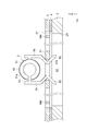
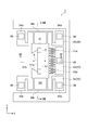
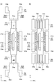
- FIG. 1 is a plan view of an optical module according to an embodiment.
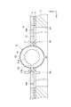
- FIG. 2 is a sectional view taken along line II-II shown in FIG.
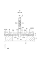
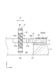
- FIG. 3 is a sectional view taken along line III-III shown in FIG. 4 is a cross-sectional view taken along the line IV-IV shown in FIG.
- FIG. 5 is a cross-sectional view taken along the line VV shown in FIG.
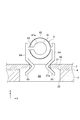
- FIG. 6 is a diagram for explaining the vibration resistance of the movable mirror and the mounting area of the comparative example.
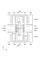
- FIG. 7 is a plan view of an optical module according to another embodiment.
- FIG. 8 is a sectional view taken along line VIII-VIII shown in FIG.
- FIG. 9 is a sectional view taken along line IX-IX shown in FIG. FIG.
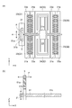
- FIG. 10 is a plan view of a modification of the movable mirror and its peripheral structure.
- FIG. 11 is a plan view of a modification of the movable mirror and its peripheral structure.
- FIG. 12 is a plan view of a modification of the movable mirror and its peripheral structure.
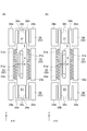
- FIG. 13 is a plan view of a modification of the movable mirror and its peripheral structure.
- the optical module 1 includes a support layer 2, a device layer 3 provided on the support layer 2, an intermediate layer 4 provided between the support layer 2 and the device layer 3, I have.
- the support layer 2, the device layer 3, and the intermediate layer 4 are configured by an SOI substrate.
- the support layer 2 is a first silicon layer of an SOI substrate.
- the device layer 3 is a second silicon layer of the SOI substrate.
- the intermediate layer 4 is an insulating layer of the SOI substrate.
- the support layer 2, the device layer 3, and the intermediate layer 4 have, for example, a rectangular shape with a side of about 10 mm when viewed from the Z-axis direction (a direction parallel to the Z-axis) that is the stacking direction thereof.
- each of the support layer 2 and the device layer 3 is, for example, about several hundred ⁇ m.
- the thickness of the intermediate layer 4 is, for example, about several ⁇ m.
- the device layer 3 and the intermediate layer 4 are shown with one corner of the device layer 3 and one corner of the intermediate layer 4 cut out.
- the device layer 3 has a mounting area 31 and a drive area 32 connected to the mounting area 31.
- the drive region 32 includes a pair of actuator regions 33 and a pair of elastic support regions 34.
- the mounting region 31 and the drive region 32 (that is, the mounting region 31 and the pair of actuator regions 33 and the pair of elastic support regions 34) are integrally formed on a part of the device layer 3 by MEMS technology (patterning and etching). Yes.
- the pair of actuator regions 33 are disposed on both sides of the mounting region 31 in the X-axis direction (direction parallel to the X-axis orthogonal to the Z-axis). That is, the mounting area 31 is sandwiched between the pair of actuator areas 33 in the X-axis direction.
- Each actuator region 33 is fixed to the support layer 2 via the intermediate layer 4.
- a first comb tooth portion 33 a is provided on the side surface of each actuator region 33 on the mounting region 31 side.
- Each first comb-tooth portion 33 a is in a state of floating with respect to the support layer 2 by removing the intermediate layer 4 immediately below the first comb-tooth portion 33 a.
- Each actuator region 33 is provided with a first electrode 35.
- the pair of elastic support regions 34 are disposed on both sides of the mounting region 31 in the Y-axis direction (the direction parallel to the Y-axis orthogonal to the Z-axis and the X-axis). That is, the mounting region 31 is sandwiched between the pair of elastic support regions 34 in the Y-axis direction. Both end portions 34 a of each elastic support region 34 are fixed to the support layer 2 through the intermediate layer 4.
- Each elastic support region 34 has an elastic deformation portion 34b (a portion between both end portions 34a) having a structure in which a plurality of leaf springs are connected.
- the elastic deformation portion 34b of each elastic support region 34 is in a state of floating with respect to the support layer 2 by removing the intermediate layer 4 immediately below the elastic deformation portion 34b.
- a second electrode 36 is provided at each of both end portions 34 a.
- each elastic support area 34 is connected to the mounting area 31.
- the mounting region 31 is in a state of floating with respect to the support layer 2 by removing the intermediate layer 4 immediately below the mounting region 31. That is, the mounting area 31 is supported by the pair of elastic support areas 34.
- a second comb tooth portion 31 a is provided on the side surface of each mounting region 31 on the side of each actuator region 33. Each second comb tooth portion 31 a is in a state of floating with respect to the support layer 2 by removing the intermediate layer 4 immediately below the second comb tooth portion 31 a. In the first comb tooth portion 33a and the second comb tooth portion 31a facing each other, the comb teeth of the first comb tooth portion 33a are located between the comb teeth of the second comb tooth portion 31a.
- the pair of elastic support regions 34 sandwich the mounting region 31 from both sides when viewed from the direction A parallel to the X axis, and when the mounting region 31 moves along the direction A, the mounting region 31 returns to the initial position.
- an elastic force is applied to the mounting region 31. Therefore, when a voltage is applied between the first electrode 35 and the second electrode 36 and an electrostatic attractive force acts between the first comb tooth portion 33a and the second comb tooth portion 31a facing each other, the electrostatic attractive force is applied.
- the mounting region 31 is moved along the direction A to a position where the elastic force by the pair of elastic support regions 34 is balanced.
- the drive region 32 functions as an electrostatic actuator.
- the optical module 1 further includes a movable mirror 5, a fixed mirror 6, a beam splitter 7, a light incident part 8, and a light emitting part 9.
- the movable mirror 5, the fixed mirror 6, and the beam splitter 7 are arranged on the device layer 3 so as to constitute an interference optical system 10 that is a Michelson interference optical system.
- the movable mirror 5 is mounted on the mounting region 31 of the device layer 3 on one side of the beam splitter 7 in the X-axis direction.
- the mirror surface 51 a of the mirror portion 51 included in the movable mirror 5 is located on the opposite side of the support layer 2 with respect to the device layer 3.
- the mirror surface 51a is, for example, a surface perpendicular to the X-axis direction (that is, a surface perpendicular to the direction A) and faces the beam splitter 7 side.
- the fixed mirror 6 is mounted on the mounting region 37 of the device layer 3 on one side of the beam splitter 7 in the Y-axis direction.
- the mirror surface 61 a of the mirror portion 61 included in the fixed mirror 6 is located on the opposite side of the support layer 2 with respect to the device layer 3.
- the mirror surface 61a is, for example, a surface perpendicular to the Y-axis direction and faces the beam splitter 7 side.
- the light incident part 8 is mounted on the device layer 3 on the other side of the beam splitter 7 in the Y-axis direction.
- the light incident part 8 is constituted by, for example, an optical fiber and a collimating lens.
- the light incident part 8 is arranged so that measurement light is incident on the interference optical system 10 from the outside.
- the light emitting portion 9 is mounted on the device layer 3 on the other side of the beam splitter 7 in the X-axis direction.
- the light emission part 9 is comprised by the optical fiber, the collimating lens, etc., for example.
- the light emitting unit 9 is arranged to emit measurement light (interference light) from the interference optical system 10 to the outside.
- the beam splitter 7 is a cube-type beam splitter having an optical function surface 7a.
- the optical function surface 7 a is located on the opposite side of the support layer 2 with respect to the device layer 3.
- the beam splitter 7 is positioned by bringing one corner on the bottom side of the beam splitter 7 into contact with one corner of the rectangular opening 3 a formed in the device layer 3.
- the beam splitter 7 is mounted on the support layer 2 by being fixed to the support layer 2 by bonding or the like in a positioned state.
- the optical module 1 configured as described above, when the measurement light L0 is incident on the interference optical system 10 from the outside via the light incident portion 8, a part of the measurement light L0 is caused by the optical function surface 7a of the beam splitter 7.
- the reflected light travels toward the movable mirror 5, and the remaining portion of the measurement light L 0 passes through the optical function surface 7 a of the beam splitter 7 and travels toward the fixed mirror 6.
- a part of the measurement light L0 is reflected by the mirror surface 51a of the movable mirror 5, travels on the same optical path toward the beam splitter 7, and passes through the optical functional surface 7a of the beam splitter 7.
- the remaining portion of the measurement light L0 is reflected by the mirror surface 61a of the fixed mirror 6, travels toward the beam splitter 7 on the same optical path, and is reflected by the optical function surface 7a of the beam splitter 7.
- a part of the measurement light L0 transmitted through the optical functional surface 7a of the beam splitter 7 and the remaining part of the measurement light L0 reflected by the optical functional surface 7a of the beam splitter 7 become the measurement light L1 that is interference light, and the measurement light L1 is emitted to the outside from the interference optical system 10 via the light emitting unit 9.
- the optical module 1 since the movable mirror 5 can be reciprocated at high speed along the direction A, a small and highly accurate FTIR can be provided. [Movable mirror and surrounding structure]
- the movable mirror 5 includes a mirror part 51, an elastic part 52, a connecting part 53, a pair of leg parts 54, and a pair of locking parts 55. Yes.
- the movable mirror 5 configured as described below is integrally formed by MEMS technology (patterning and etching).
- the mirror part 51 is formed in a plate shape (for example, a disk shape) having the mirror surface 51a as a main surface.
- the elastic part 52 is formed in an annular shape (for example, an annular shape) surrounding the mirror part 51 while being separated from the mirror part 51 when viewed from the X-axis direction (direction perpendicular to the mirror surface 51a).
- the connecting portion 53 connects the mirror portion 51 and the elastic portion 52 to each other on one side in the Y-axis direction with respect to the center of the mirror portion 51 when viewed from the X-axis direction.
- the pair of leg portions 54 are connected to the outer surface of the elastic portion 52 on both sides in the Y-axis direction with respect to the center of the mirror portion 51 when viewed from the X-axis direction. That is, the mirror part 51 and the elastic part 52 are sandwiched between the pair of leg parts 54 in the Y-axis direction. Each leg portion 54 extends closer to the mounting region 31 than the mirror portion 51 and the elastic portion 52.
- the pair of locking portions 55 are provided at the end portions on the mounting region 31 side of the respective leg portions 54. Each locking portion 55 is formed so as to be bent in, for example, a V shape on the inner side (side closer to each other) when viewed from the X-axis direction.
- the movable mirror 5 configured as described above is mounted in the mounting region 31 by arranging the pair of locking portions 55 in the opening 31b formed in the mounting region 31.
- the openings 31b are opened on both sides of the mounting region 31 in the Z-axis direction. A part of each locking portion 55 protrudes from the surface on the intermediate layer 4 side in the mounting region 31. That is, the movable mirror 5 penetrates the mounting area 31.
- a force is applied to the pair of locking portions 55 arranged in the opening 31b of the mounting region 31 on the outer side (side away from each other).
- the movable mirror 5 is fixed to the mounting region 31 by the force.
- the force is generated when the annular elastic portion 52 compressed when the movable mirror 5 is mounted on the mounting region 31 is restored to the initial state.
- the opening 31 b is formed in a trapezoidal shape spreading toward the opposite side to the beam splitter 7 when viewed from the Z-axis direction.
- the movable mirror 5 is automatically operated in each of the X-axis direction, the Y-axis direction, and the Z-axis direction by engaging the pair of locking portions 55 having a shape bent inward with the opening 31b having such a shape. Positioned (self-aligned).
- the intermediate layer 4 has an opening (first opening) 41 formed therein.
- the openings 41 are open on both sides of the intermediate layer 4 in the Z-axis direction.
- An opening (second opening) 21 is formed in the support layer 2.
- the openings 21 are open on both sides of the support layer 2 in the Z-axis direction.
- a continuous space S ⁇ b> 1 is configured by the region in the opening 41 of the intermediate layer 4 and the region in the opening 21 of the support layer 2. That is, the space S ⁇ b> 1 includes a region in the opening 41 of the intermediate layer 4 and a region in the opening 21 of the support layer 2.
- the space S ⁇ b> 1 is formed between the support layer 2 and the device layer 3 and corresponds to at least the mounting region 31 and the drive region 32.
- the region in the opening 41 of the intermediate layer 4 and the region in the opening 21 of the support layer 2 include a range in which the mounting region 31 moves when viewed from the Z-axis direction.
- a region in the opening 41 of the intermediate layer 4 is a portion to be separated from the support layer 2 in the mounting region 31 and the drive region 32 (that is, a portion to be floated with respect to the support layer 2, for example,
- a gap for separating the entire mounting region 31, the elastic deformation portion 34 b of each elastic support region 34, the first comb tooth portion 33 a and the second comb tooth portion 31 a) from the support layer 2 is formed.
- the space S1 corresponding to at least the mounting region 31 and the drive region 32 is the support layer 2 and the device layer so that the entire mounting region 31 and at least a part of the drive region 32 are separated from the support layer 2.
- 3 means a space formed between the two.
- each locking portion 55 of the movable mirror 5 is located in the space S1. Specifically, a part of each locking portion 55 is located in a region in the opening 21 of the support layer 2 via a region in the opening 41 of the intermediate layer 4. A part of each locking portion 55 protrudes from the surface of the device layer 3 on the intermediate layer 4 side into the space S1, for example, about 100 ⁇ m. As described above, the region in the opening 41 of the intermediate layer 4 and the region in the opening 21 of the support layer 2 include a range in which the mounting region 31 moves when viewed from the Z-axis direction. Is reciprocated along the direction A, a part of each locking portion 55 of the movable mirror 5 located in the space S1 does not come into contact with the intermediate layer 4 and the support layer 2. [Fixed mirror and its peripheral structure]
- the fixed mirror 6 includes a mirror part 61, an elastic part 62, a connecting part 63, a pair of leg parts 64, and a pair of locking parts 65. Yes.
- the fixed mirror 6 configured as follows is integrally formed by MEMS technology (patterning and etching).
- the mirror part 61 is formed in a plate shape (for example, a disk shape) having the mirror surface 61a as a main surface.
- the elastic part 62 is formed in an annular shape (for example, an annular shape) surrounding the mirror part 61 while being separated from the mirror part 61 when viewed from the Y-axis direction (direction perpendicular to the mirror surface 61a).
- the connecting part 63 connects the mirror part 61 and the elastic part 62 to each other on one side in the X-axis direction with respect to the center of the mirror part 61 when viewed from the Y-axis direction.
- the pair of leg portions 64 are connected to the outer surface of the elastic portion 62 on both sides in the X-axis direction with respect to the center of the mirror portion 61 when viewed from the Y-axis direction. That is, the mirror part 61 and the elastic part 62 are sandwiched between the pair of leg parts 64 in the X-axis direction. Each leg portion 64 extends closer to the mounting region 37 than the mirror portion 61 and the elastic portion 62.
- the pair of locking portions 65 are provided at the end portions on the mounting region 37 side of the respective leg portions 64. Each locking portion 65 is formed to be bent in, for example, a V shape on the inner side (side closer to each other) when viewed from the Y-axis direction.
- the fixed mirror 6 configured as described above is mounted in the mounting region 37 by arranging the pair of locking portions 65 in the opening 37 a formed in the mounting region 37.
- the openings 37a are opened on both sides of the mounting region 37 in the Z-axis direction. A part of each locking portion 65 protrudes from the surface on the intermediate layer 4 side in the mounting region 37. That is, the fixed mirror 6 penetrates the mounting area 37.
- a force is applied to the pair of locking portions 65 disposed in the opening 37a of the mounting region 37 on the outer side (side away from each other).
- the fixed mirror 6 is fixed to the mounting area 37 by the force.
- the force is generated when the annular elastic portion 62 compressed when the fixed mirror 6 is mounted in the mounting region 37 is restored to the initial state.
- the opening 37a is formed in a trapezoidal shape spreading toward the opposite side to the beam splitter 7 when viewed from the Z-axis direction.
- the fixed mirror 6 is automatically operated in each of the X-axis direction, the Y-axis direction, and the Z-axis direction by engaging the pair of locking portions 65 that are bent inward with the opening 37a having such a shape. Positioned (self-aligned).
- the intermediate layer 4 has an opening 42 formed therein.
- the opening 42 includes the opening 37a of the mounting region 37 when viewed from the Z-axis direction, and opens on both sides of the intermediate layer 4 in the Z-axis direction.
- An opening 22 is formed in the support layer 2.
- the opening 22 includes the opening 37a of the mounting region 37 when viewed from the Z-axis direction, and opens on both sides of the support layer 2 in the Z-axis direction.
- a continuous space S ⁇ b> 2 is configured by the region in the opening 42 of the intermediate layer 4 and the region in the opening 22 of the support layer 2. That is, the space S ⁇ b> 2 includes a region in the opening 42 of the intermediate layer 4 and a region in the opening 22 of the support layer 2.
- each locking portion 65 of the fixed mirror 6 is located in the space S2. Specifically, a part of each locking portion 65 is located in a region in the opening 22 of the support layer 2 via a region in the opening 42 of the intermediate layer 4. A part of each locking portion 65 protrudes from the surface of the device layer 3 on the intermediate layer 4 side into the space S2, for example, about 100 ⁇ m.
- the mounting region 31 on which the movable mirror 5 is mounted is sandwiched between a pair of elastic support regions 34 and supported by the pair of elastic support regions 34.
- the mounting region 31 on which the movable mirror 5 is mounted can be stably moved as compared with the case where the region extending from the mounting region 31 is supported by the elastic support region 34. Therefore, according to the optical module 1, the reliable movement of the movable mirror 5 mounted on the device layer 3 is realized.
- the vibration resistance of the mounting region 31 along the Y-axis direction As shown in FIGS. 6A and 6B, in the configuration in which the region 31 c extending from the mounting region 31 is supported by the elastic support region 34, the vibration resistance of the mounting region 31 along the Y-axis direction. (Arrow ⁇ shown in FIG. 6A), vibration resistance of the mounting region 31 along the Z-axis direction (arrow ⁇ shown in FIG. 6B), and the movable mirror 5 along the X-axis direction Vibration resistance (arrow ⁇ shown in FIG. 6B) tends to be low.
- the configuration of the optical module 1 it is possible to improve the vibration resistance of the mounting region 31 along the Y-axis direction and the vibration resistance of the mounting region 31 along the Z-axis direction.
- the first electrode 35 and the second electrode 36 are not shown.
- the support layer 2 is the first silicon layer of the SOI substrate
- the device layer 3 is the second silicon layer of the SOI substrate
- the intermediate layer 4 is the insulating layer of the SOI substrate.
- the pair of elastic support regions 34 sandwich the mounting region 31 from both sides when viewed from the direction A in which the mounting region 31 moves. Thereby, the structure for the reliable movement of the movable mirror 5 mounted in the device layer 3 can be simplified.
- the movable mirror 5, the fixed mirror 6, and the beam splitter 7 are arranged so as to constitute the interference optical system 10. Thereby, FTIR with improved sensitivity can be obtained.
- the light incident part 8 is arranged so that the measurement light is incident on the interference optical system 10 from the outside, and the light emitting part 9 emits the measurement light from the interference optical system 10 to the outside.
- the light emitting part 9 emits the measurement light from the interference optical system 10 to the outside.
- this indication is not limited to the above-mentioned embodiment.
- the materials and shapes of each component are not limited to the materials and shapes described above, and various materials and shapes can be employed.
- the shape of the mirror part 51 and the mirror surface 51a is not limited to a circular shape, and may be other shapes such as a rectangular shape.
- the space S1 is formed between the support layer 2 and the device layer 3, and various modes can be adopted as long as it corresponds to at least the mounting region 31 and the drive region 32.
- a recess that opens to the device layer 3 side is formed in the support layer 2, and the space S ⁇ b> 1 is configured by the region in the opening 41 of the intermediate layer 4 and the region in the recess of the support layer 2. It may be.
- the support layer 2 and the device layer 3 may be bonded to each other without the intermediate layer 4 interposed therebetween.
- the support layer 2 is formed of, for example, silicon, glass, ceramic, and the like
- the device layer 3 is formed of, for example, silicon.
- the support layer 2 and the device layer 3 are bonded to each other by, for example, direct bonding, surface activation bonding, plasma bonding, anode bonding, metal bonding, resin bonding, or the like.
- the space S1 is formed between the support layer 2 and the device layer 3, and includes at least the mounting region 31 and As long as it corresponds to the drive region 32, various modes can be adopted.
- the space S ⁇ b> 1 may be configured by openings formed in the support layer 2 so as to open on both sides of the support layer 2.
- the space S ⁇ b> 1 may be configured by a recess formed in the support layer 2 so as to open to the device layer 3 side.
- the space S1 may be configured by an opening formed in the support layer 2 so as to open on both sides of the support layer 2 and a recess formed in the device layer 3 so as to open on the support layer 2 side.
- the space S ⁇ b> 1 may be configured by a recess formed in the support layer 2 so as to open toward the device layer 3 and a recess formed in the device layer 3 so as to open toward the support layer 2.
- the space S1 may be configured by a recess formed in the device layer 3 so as to open to the support layer 2 side.
- the movable mirror 5 may penetrate the mounting region 31 with the mirror surface 51 a intersecting the mounting region 31.
- the pair of legs 54 is not provided on the movable mirror 5, and the pair of locking portions 55 are mirror portions when viewed from the X-axis direction.
- the elastic member 52 is connected to the outer surface on both sides in the Y-axis direction with respect to the center of 51. That is, the mirror part 51 and the elastic part 52 are sandwiched between the pair of locking parts 55 in the Y-axis direction.
- a portion that defines the opening 31 b and is opposed to the mirror surface 51 a is cut out to allow the measurement light L 0 to pass therethrough.
- the mirror surface 51 a of the movable mirror 5 intersects the mounting region 31. Thereby, since the gravity center position of the movable mirror 5 can be brought close to the mounting area 31, the mounting area 31 on which the movable mirror 5 is mounted can be moved more stably.
- the vibration resistance of the mounting region 31 along the Y-axis direction (the arrow shown in FIG. 6A).
- vibration resistance of the mounting region 31 along the Z-axis direction (arrow ⁇ shown in FIG. 6B)
- vibration resistance of the movable mirror 5 along the X-axis direction (FIG. 6B).
- the arrow ⁇ ) shown tends to be low.
- the vibration resistance of the mounting region 31 along the Y-axis direction, the vibration resistance of the mounting region 31 along the Z-axis direction, and X The vibration resistance of the movable mirror 5 along the axial direction can be improved.
- the drive region 32 can adopt various modes as long as the pair of elastic support regions 34 support the mounting region 31 in between.
- a pair of spring portions 34c connected to the mounting region 31 in the elastic deformation portion 34b may be connected to each other as shown in FIG. Alternatively, as shown in FIG. 10B, they may be separated from each other.
- a pair of spring part 34d connected to each of the both ends 34a among the elastic deformation parts 34b is a side opposite to the mounting area
- the elastic deformation part 34b may have three or more spring parts 34c, as FIG.11 (b) shows.
- the pair of spring portions 34c of the elastic deformation portion 34b may be connected to both side surfaces of the mounting region 31 in the X-axis direction, as shown in FIG. Further, as shown in FIGS. 13A and 13B, the pair of elastic support regions 34 may be disposed on both sides of the mounting region 31 in the X-axis direction. 10 to 13, the illustration of the first electrode 35 and the second electrode 36 is omitted.
- the spring portions 34b of each elastic support region 34 include a plurality of spring portions 34c.
- the other end of each spring portion 34c is connected to each other via a beam-shaped portion 34e. According to this configuration, unnecessary vibration of the movable mirror 5 can be more reliably suppressed as compared with the case where the other end portions of the spring portions 34c are not connected to each other.
- this configuration is effective when the elastic deformation portion 34b of each elastic support region 34 includes a pair of spring portions 34c.
- the distance (interval) between the spring portions 34c adjacent to each other in the elastic deformation portion 34b of each elastic support region 34 is movable.
- the center of gravity of the movable mirror 5 in the direction A in which the mounting area 31 moves is one spring portion 34c (in the direction A).
- One end of one of the spring portions 34c adjacent to each other (the end connected to the mounting region 31) (hereinafter referred to as “connection end”) and the other spring portion 34c in the direction A (adjacent to each other) It is preferable to be located between the other end of the spring portion 34c and the position of the connection end.
- These positions are the positions in the direction A (X coordinates in FIG. 10A, FIG. 11A, and FIG. 12). According to this configuration, unnecessary vibration of the movable mirror 5 can be suppressed while securing the amount of movement of the mounting region 31 without increasing the number of spring portions 34c in the elastic deformation portions 34b of the elastic support regions 34. it can. In particular, this configuration is effective when the elastic deformation portion 34b of each elastic support region 34 includes a pair of spring portions 34c.
- each elastic support region 34 when the elastic deformation portion 34 b of each elastic support region 34 includes a pair of spring portions 34 c, each elastic support region 34.
- the distance (interval) between the spring portions 34c adjacent to each other in the elastic deformation portion 34b is the first distance from one end portion of the mounting region 31 in the direction A to the connection end portion of one spring portion 34c, and the mounting in the direction A. It is preferable that the distance is larger than the second distance from the other end of the region 31 to the connection end of the other spring portion 34c.
- the first distance and the second distance are more preferably equal. According to this configuration, unnecessary vibration of the movable mirror 5 can be suppressed while securing the amount of movement of the mounting region 31 without increasing the number of spring portions 34c in the elastic deformation portions 34b of the elastic support regions 34. it can.
- the fixed mirror 6 is mounted on the device layer 3, but the fixed mirror 6 may be mounted on at least one of the support layer 2, the device layer 3, and the intermediate layer 4.
- the beam splitter 7 is mounted on the support layer 2. However, the beam splitter 7 may be mounted on at least one of the support layer 2, the device layer 3, and the intermediate layer 4.
- the beam splitter 7 is not limited to a cube type beam splitter, and may be a plate type beam splitter.
- the optical module 1 may include a light emitting element that generates measurement light incident on the light incident portion 8 in addition to the light incident portion 8.
- the optical module 1 may include a light emitting element that generates measurement light incident on the interference optical system 10 instead of the light incident portion 8.
- the optical module 1 may include a light receiving element that detects measurement light (interference light) emitted from the light emitting unit 9 in addition to the light emitting unit 9.
- the optical module 1 may include a light receiving element that detects measurement light (interference light) emitted from the interference optical system 10 instead of the light emitting unit 9.
- first through electrode electrically connected to each actuator region 33 and the second through electrode electrically connected to each of both end portions 34a of each elastic support region 34 are the support layer 2 and the intermediate layer 4. (Only the support layer 2 when the intermediate layer 4 does not exist) may be provided, and a voltage may be applied between the first through electrode and the second through electrode.
- the actuator that moves the mounting region 31 is not limited to an electrostatic actuator, and may be a piezoelectric actuator, an electromagnetic actuator, or the like.
- the optical module 1 is not limited to what comprises FTIR, and may comprise another optical system.
- SYMBOLS 1 Optical module, 2 ... Support layer, 3 ... Device layer, 4 ... Intermediate layer, 5 ... Movable mirror, 6 ... Fixed mirror, 7 ... Beam splitter, 8 ... Light incident part, 9 ... Light emitting part, 10 ... Interference Optical system 31 ... Mounting region 32 ... Drive region 34 ... Elastic support region 41 ... Opening 51a ... Mirror surface S1 ... Space.
Landscapes
- Physics & Mathematics (AREA)
- Spectroscopy & Molecular Physics (AREA)
- General Physics & Mathematics (AREA)
- Optics & Photonics (AREA)
- Life Sciences & Earth Sciences (AREA)
- Biochemistry (AREA)
- Computer Hardware Design (AREA)
- Health & Medical Sciences (AREA)
- Engineering & Computer Science (AREA)
- Chemical & Material Sciences (AREA)
- Analytical Chemistry (AREA)
- Microelectronics & Electronic Packaging (AREA)
- General Health & Medical Sciences (AREA)
- Immunology (AREA)
- Pathology (AREA)
- Mechanical Light Control Or Optical Switches (AREA)
- Micromachines (AREA)
- Spectrometry And Color Measurement (AREA)
Abstract
本発明の光モジュールは、支持層(2)と、支持層(2)上に設けられたデバイス層(3)と、デバイス層(3)に実装された可動ミラー(5)と、を備える。デバイス層(3)は、可動ミラー(5)が実装された実装領域(31)と、実装領域(31)に接続された駆動領域(32)と、を有する。支持層(2)とデバイス層(3)との間には、少なくとも実装領域(31)及び駆動領域(32)に対応する空間(S1)が形成されている。実装領域(31)は、駆動領域(32)に含まれる一対の弾性支持領域(34)に挟まれており、一対の弾性支持領域(34)によって支持されている。
Description
本開示は、光モジュールに関する。
MEMS(Micro Electro Mechanical Systems)技術によってSOI(Silicon On Insulator)基板に干渉光学系が形成された光モジュールが知られている(例えば、特許文献1参照)。このような光モジュールは、高精度な光学配置が実現されたFTIR(フーリエ変換型赤外分光分析器)を提供し得るため、注目されている。
しかし、上述したような光モジュールには、例えば可動ミラーのサイズがSOI基板に対する深堀加工の達成度に依存する点で、次のような課題がある。すなわち、SOI基板に対する深堀加工の達成度は最大でも500μm程度であるため、可動ミラーのサイズを大きくしてFTIRにおける感度を向上させるのには限界がある。そこで、別体で形成された可動ミラーをデバイス層(例えばSOI基板において駆動領域が形成される層)に実装する技術が考えられる。
本開示は、デバイス層に実装された可動ミラーの確実な移動が実現された光モジュールを提供することを目的とする。
本開示の一側面の光モジュールは、支持層と、支持層上に設けられたデバイス層と、デバイス層に実装された可動ミラーと、を備え、デバイス層は、可動ミラーが実装された実装領域と、実装領域に接続された駆動領域と、を有し、支持層とデバイス層との間には、少なくとも実装領域及び駆動領域に対応する空間が形成されており、実装領域は、駆動領域に含まれる一対の弾性支持領域に挟まれており、一対の弾性支持領域によって支持されている。
この光モジュールでは、デバイス層において、可動ミラーが実装された実装領域が、一対の弾性支持領域に挟まれており、一対の弾性支持領域によって支持されている。これにより、例えば、実装領域から延在する領域が弾性支持領域によって支持されているような場合に比べ、可動ミラーが実装された実装領域を安定的に移動させることができる。よって、この光モジュールによれば、デバイス層に実装された可動ミラーの確実な移動が実現される。
本開示の一側面の光モジュールは、支持層とデバイス層との間に設けられた中間層を更に備え、中間層には、開口が形成されており、空間は、開口内の領域を含み、支持層は、SOI基板の第1シリコン層であり、デバイス層は、SOI基板の第2シリコン層であり、中間層は、SOI基板の絶縁層であってもよい。これによれば、デバイス層に実装された可動ミラーの確実な移動のための構成をSOI基板によって好適に実現することができる。
本開示の一側面の光モジュールでは、一対の弾性支持領域は、実装領域が移動する方向から見た場合に両側から実装領域を挟んでいてもよい。これによれば、デバイス層に実装された可動ミラーの確実な移動のための構成を簡易化することができる。
本開示の一側面の光モジュールでは、可動ミラーのミラー面は、実装領域と交差していてもよい。これによれば、可動ミラーの重心位置を実装領域に近付けることができるので、可動ミラーが実装された実装領域をより安定的に移動させることができる。
本開示の一側面の光モジュールは、支持層、デバイス層、及び支持層とデバイス層との間に設けられた中間層の少なくとも1つに実装された固定ミラーと、支持層、デバイス層、及び中間層の少なくとも1つに実装されたビームスプリッタと、を更に備え、可動ミラー、固定ミラー及びビームスプリッタは、干渉光学系を構成するように配置されていてもよい。これによれば、感度が向上されたFTIRを得ることができる。
本開示の一側面の光モジュールは、外部から干渉光学系に測定光を入射させるように配置された光入射部と、干渉光学系から外部に測定光を出射させるように配置された光出射部と、を更に備えてもよい。これによれば、光入射部及び光出射部を備えるFTIRを得ることができる。
本開示によれば、デバイス層に実装された可動ミラーの確実な移動が実現された光モジュールを提供することができる。
以下、本開示の実施形態について、図面を参照して詳細に説明する。なお、各図において同一又は相当部分には同一符号を付し、重複する部分を省略する。
[光モジュールの構成]
[光モジュールの構成]
図1に示されるように、光モジュール1は、支持層2と、支持層2上に設けられたデバイス層3と、支持層2とデバイス層3との間に設けられた中間層4と、備えている。支持層2、デバイス層3及び中間層4は、SOI基板によって構成されている。具体的には、支持層2は、SOI基板の第1シリコン層である。デバイス層3は、SOI基板の第2シリコン層である。中間層4は、SOI基板の絶縁層である。支持層2、デバイス層3及び中間層4は、それらの積層方向であるZ軸方向(Z軸に平行な方向)から見た場合に、例えば、一辺が10mm程度の矩形状を呈している。支持層2及びデバイス層3のそれぞれの厚さは、例えば数百μm程度である。中間層4の厚さは、例えば数μm程度である。なお、図1では、デバイス層3の1つの角部及び中間層4の1つの角部が切り欠かれた状態で、デバイス層3及び中間層4が示されている。
デバイス層3は、実装領域31と、実装領域31に接続された駆動領域32と、を有している。駆動領域32は、一対のアクチュエータ領域33と、一対の弾性支持領域34と、を含んでいる。実装領域31及び駆動領域32(すなわち、実装領域31並びに一対のアクチュエータ領域33及び一対の弾性支持領域34)は、MEMS技術(パターニング及びエッチング)によってデバイス層3の一部に一体的に形成されている。
一対のアクチュエータ領域33は、X軸方向(Z軸に直交するX軸に平行な方向)において実装領域31の両側に配置されている。つまり、実装領域31は、X軸方向において一対のアクチュエータ領域33に挟まれている。各アクチュエータ領域33は、中間層4を介して支持層2に固定されている。各アクチュエータ領域33における実装領域31側の側面には、第1櫛歯部33aが設けられている。各第1櫛歯部33aは、その直下の中間層4が除去されることで、支持層2に対して浮いた状態となっている。各アクチュエータ領域33には、第1電極35が設けられている。
一対の弾性支持領域34は、Y軸方向(Z軸及びX軸に直交するY軸に平行な方向)において実装領域31の両側に配置されている。つまり、実装領域31は、Y軸方向において一対の弾性支持領域34に挟まれている。各弾性支持領域34の両端部34aは、中間層4を介して支持層2に固定されている。各弾性支持領域34の弾性変形部34b(両端部34aの間の部分)は、複数の板バネが連結された構造を有している。各弾性支持領域34の弾性変形部34bは、その直下の中間層4が除去されることで、支持層2に対して浮いた状態となっている。各弾性支持領域34において両端部34aのそれぞれには、第2電極36が設けられている。
実装領域31には、各弾性支持領域34の弾性変形部34bが接続されている。実装領域31は、その直下の中間層4が除去されることで、支持層2に対して浮いた状態となっている。つまり、実装領域31は、一対の弾性支持領域34によって支持されている。実装領域31における各アクチュエータ領域33側の側面には、第2櫛歯部31aが設けられている。各第2櫛歯部31aは、その直下の中間層4が除去されることで、支持層2に対して浮いた状態となっている。互いに対向する第1櫛歯部33a及び第2櫛歯部31aにおいては、第1櫛歯部33aの各櫛歯が第2櫛歯部31aの各櫛歯間に位置している。
一対の弾性支持領域34は、X軸に平行な方向Aから見た場合に両側から実装領域31を挟んでおり、実装領域31が方向Aに沿って移動すると、実装領域31が初期位置に戻るように実装領域31に弾性力を作用させる。したがって、第1電極35と第2電極36との間に電圧が印加されて、互いに対向する第1櫛歯部33a及び第2櫛歯部31a間に静電引力が作用すると、当該静電引力と一対の弾性支持領域34による弾性力とがつり合う位置まで、方向Aに沿って実装領域31が移動させられる。このように、駆動領域32は、静電アクチュエータとして機能する。
光モジュール1は、可動ミラー5と、固定ミラー6と、ビームスプリッタ7と、光入射部8と、光出射部9と、を更に備えている。可動ミラー5、固定ミラー6及びビームスプリッタ7は、マイケルソン干渉光学系である干渉光学系10を構成するように、デバイス層3上に配置されている。
可動ミラー5は、X軸方向におけるビームスプリッタ7の一方の側において、デバイス層3の実装領域31に実装されている。可動ミラー5が有するミラー部51のミラー面51aは、デバイス層3に対して支持層2とは反対側に位置している。ミラー面51aは、例えばX軸方向に垂直な面(すなわち、方向Aに垂直な面)であり、ビームスプリッタ7側に向いている。
固定ミラー6は、Y軸方向におけるビームスプリッタ7の一方の側において、デバイス層3の実装領域37に実装されている。固定ミラー6が有するミラー部61のミラー面61aは、デバイス層3に対して支持層2とは反対側に位置している。ミラー面61aは、例えばY軸方向に垂直な面であり、ビームスプリッタ7側に向いている。
光入射部8は、Y軸方向におけるビームスプリッタ7の他方の側において、デバイス層3に実装されている。光入射部8は、例えば光ファイバ及びコリメートレンズ等によって構成されている。光入射部8は、外部から干渉光学系10に測定光を入射させるように配置されている。
光出射部9は、X軸方向におけるビームスプリッタ7の他方の側において、デバイス層3に実装されている。光出射部9は、例えば光ファイバ及びコリメートレンズ等によって構成されている。光出射部9は、干渉光学系10から外部に測定光(干渉光)を出射させるように配置されている。
ビームスプリッタ7は、光学機能面7aを有するキューブタイプのビームスプリッタである。光学機能面7aは、デバイス層3に対して支持層2とは反対側に位置している。ビームスプリッタ7は、デバイス層3に形成された矩形状の開口3aの1つの隅部にビームスプリッタ7の底面側の1つの角部が接触させられることで、位置決めされている。ビームスプリッタ7は、位置決めされた状態で接着等によって支持層2に固定されることで、支持層2に実装されている。
以上のように構成された光モジュール1では、光入射部8を介して外部から干渉光学系10に測定光L0が入射すると、測定光L0の一部は、ビームスプリッタ7の光学機能面7aで反射されて可動ミラー5に向かって進行し、測定光L0の残部は、ビームスプリッタ7の光学機能面7aを透過して固定ミラー6に向かって進行する。測定光L0の一部は、可動ミラー5のミラー面51aで反射されて、同一光路上をビームスプリッタ7に向かって進行し、ビームスプリッタ7の光学機能面7aを透過する。測定光L0の残部は、固定ミラー6のミラー面61aで反射されて、同一光路上をビームスプリッタ7に向かって進行し、ビームスプリッタ7の光学機能面7aで反射される。ビームスプリッタ7の光学機能面7aを透過した測定光L0の一部と、ビームスプリッタ7の光学機能面7aで反射された測定光L0の残部とは、干渉光である測定光L1となり、測定光L1は、光出射部9を介して干渉光学系10から外部に出射する。光モジュール1によれば、方向Aに沿って可動ミラー5を高速で往復動させることができるので、小型且つ高精度のFTIRを提供することができる。
[可動ミラー及びその周辺構造]
[可動ミラー及びその周辺構造]
図2及び図3に示されるように、可動ミラー5は、ミラー部51と、弾性部52と、連結部53と、一対の脚部54と、一対の係止部55と、を有している。以下のように構成される可動ミラー5は、MEMS技術(パターニング及びエッチング)によって一体的に形成されている。
ミラー部51は、ミラー面51aを主面として有する板状(例えば、円板状)に形成されている。弾性部52は、X軸方向(ミラー面51aに垂直な方向)から見た場合にミラー部51から離間しつつミラー部51を囲む環状(例えば、円環状)に形成されている。連結部53は、X軸方向から見た場合にミラー部51の中心に対してY軸方向における一方の側において、ミラー部51と弾性部52とを互いに連結している。
一対の脚部54は、X軸方向から見た場合にミラー部51の中心に対してY軸方向における両側において、弾性部52における外側の表面に連結されている。つまり、ミラー部51及び弾性部52は、Y軸方向において一対の脚部54に挟まれている。各脚部54は、ミラー部51及び弾性部52よりも実装領域31側に延在している。一対の係止部55は、各脚部54における実装領域31側の端部にそれぞれ設けられている。各係止部55は、X軸方向から見た場合に内側(互いに近づく側)に例えばV字状に屈曲するように形成されている。
以上のように構成された可動ミラー5は、実装領域31に形成された開口31bに一対の係止部55が配置されることで、実装領域31に実装されている。開口31bは、Z軸方向において実装領域31の両側に開口している。各係止部55の一部は、実装領域31における中間層4側の表面から突出している。つまり、可動ミラー5は、実装領域31を貫通している。
実装領域31の開口31bに配置された一対の係止部55には、外側(互いに遠ざかる側)に力が作用している。可動ミラー5は、当該力によって実装領域31に固定されている。当該力は、可動ミラー5が実装領域31に実装される際に圧縮された環状の弾性部52が初期状態に復元しようとして生じているものである。
なお、図1に示されるように、開口31bは、Z軸方向から見た場合にビームスプリッタ7とは反対側に末広がりの台形状に形成されている。このような形状を呈する開口31bに、内側に屈曲する形状を呈する一対の係止部55が係合することで、可動ミラー5は、X軸方向、Y軸方向及びZ軸方向のそれぞれにおいて自動的に位置決めされる(セルフアライメントされる)。
図2及び図3に示されるように、中間層4には、開口(第1開口)41が形成されている。開口41は、Z軸方向において中間層4の両側に開口している。支持層2には、開口(第2開口)21が形成されている。開口21は、Z軸方向において支持層2の両側に開口している。光モジュール1では、中間層4の開口41内の領域及び支持層2の開口21内の領域によって、一続きの空間S1が構成されている。つまり、空間S1は、中間層4の開口41内の領域及び支持層2の開口21内の領域を含んでいる。
空間S1は、支持層2とデバイス層3との間に形成されており、少なくとも実装領域31及び駆動領域32に対応している。具体的には、中間層4の開口41内の領域及び支持層2の開口21内の領域は、Z軸方向から見た場合に実装領域31が移動する範囲を含んでいる。中間層4の開口41内の領域は、実装領域31及び駆動領域32のうち支持層2から離間させるべき部分(すなわち、支持層2に対して浮いた状態とすべき部分であって、例えば、実装領域31の全体、各弾性支持領域34の弾性変形部34b、第1櫛歯部33a及び第2櫛歯部31a)を支持層2から離間させるための隙間を形成している。つまり、少なくとも実装領域31及び駆動領域32に対応する空間S1とは、実装領域31の全体と、駆動領域32の少なくとも一部と、が支持層2から離間するように、支持層2とデバイス層3との間に形成された空間を意味する。
空間S1には、可動ミラー5が有する各係止部55の一部が位置している。具体的には、各係止部55の一部は、中間層4の開口41内の領域を介して、支持層2の開口21内の領域に位置している。各係止部55の一部は、デバイス層3における中間層4側の表面から空間S1内に、例えば100μm程度突出している。上述したように、中間層4の開口41内の領域及び支持層2の開口21内の領域は、Z軸方向から見た場合に実装領域31が移動する範囲を含んでいるため、実装領域31が方向Aに沿って往復動した際に、可動ミラー5の各係止部55うち空間S1に位置する一部が、中間層4及び支持層2と接触することはない。
[固定ミラー及びその周辺構造]
[固定ミラー及びその周辺構造]
図4及び図5に示されるように、固定ミラー6は、ミラー部61と、弾性部62と、連結部63と、一対の脚部64と、一対の係止部65と、を有している。以下のように構成される固定ミラー6は、MEMS技術(パターニング及びエッチング)によって一体的に形成されている。
ミラー部61は、ミラー面61aを主面として有する板状(例えば、円板状)に形成されている。弾性部62は、Y軸方向(ミラー面61aに垂直な方向)から見た場合にミラー部61から離間しつつミラー部61を囲む環状(例えば、円環状)に形成されている。連結部63は、Y軸方向から見た場合にミラー部61の中心に対してX軸方向における一方の側において、ミラー部61と弾性部62とを互いに連結している。
一対の脚部64は、Y軸方向から見た場合にミラー部61の中心に対してX軸方向における両側において、弾性部62における外側の表面に連結されている。つまり、ミラー部61及び弾性部62は、X軸方向において一対の脚部64に挟まれている。各脚部64は、ミラー部61及び弾性部62よりも実装領域37側に延在している。一対の係止部65は、各脚部64における実装領域37側の端部にそれぞれ設けられている。各係止部65は、Y軸方向から見た場合に内側(互いに近づく側)に例えばV字状に屈曲するように形成されている。
以上のように構成された固定ミラー6は、実装領域37に形成された開口37aに一対の係止部65が配置されることで、実装領域37に実装されている。開口37aは、Z軸方向において実装領域37の両側に開口している。各係止部65の一部は、実装領域37における中間層4側の表面から突出している。つまり、固定ミラー6は、実装領域37を貫通している。
実装領域37の開口37aに配置された一対の係止部65には、外側(互いに遠ざかる側)に力が作用している。固定ミラー6は、当該力によって実装領域37に固定されている。当該力は、固定ミラー6が実装領域37に実装される際に圧縮された環状の弾性部62が初期状態に復元しようとして生じているものである。
なお、図1に示されるように、開口37aは、Z軸方向から見た場合にビームスプリッタ7とは反対側に末広がりの台形状に形成されている。このような形状を呈する開口37aに、内側に屈曲する形状を呈する一対の係止部65が係合することで、固定ミラー6は、X軸方向、Y軸方向及びZ軸方向のそれぞれにおいて自動的に位置決めされる(セルフアライメントされる)。
図4及び図5に示されるように、中間層4には、開口42が形成されている。開口42は、Z軸方向から見た場合に実装領域37の開口37aを含んでおり、Z軸方向において中間層4の両側に開口している。支持層2には、開口22が形成されている。開口22は、Z軸方向から見た場合に実装領域37の開口37aを含んでおり、Z軸方向において支持層2の両側に開口している。光モジュール1では、中間層4の開口42内の領域及び支持層2の開口22内の領域によって、一続きの空間S2が構成されている。つまり、空間S2は、中間層4の開口42内の領域及び支持層2の開口22内の領域を含んでいる。
空間S2には、固定ミラー6が有する各係止部65の一部が位置している。具体的には、各係止部65の一部は、中間層4の開口42内の領域を介して、支持層2の開口22内の領域に位置している。各係止部65の一部は、デバイス層3における中間層4側の表面から空間S2内に、例えば100μm程度突出している。
[作用及び効果]
[作用及び効果]
光モジュール1では、デバイス層3において、可動ミラー5が実装された実装領域31が、一対の弾性支持領域34に挟まれており、一対の弾性支持領域34によって支持されている。これにより、例えば、実装領域31から延在する領域が弾性支持領域34によって支持されているような場合に比べ、可動ミラー5が実装された実装領域31を安定的に移動させることができる。よって、光モジュール1によれば、デバイス層3に実装された可動ミラー5の確実な移動が実現される。
図6の(a)及び(b)に示されるように、実装領域31から延在する領域31cが弾性支持領域34によって支持されている構成では、Y軸方向に沿った実装領域31の振動耐性(図6の(a)に示される矢印α)、Z軸方向に沿った実装領域31の振動耐性(図6の(b)に示される矢印β)、及びX軸方向に沿った可動ミラー5の振動耐性(図6の(b)に示される矢印γ)が低くなり易い。これに対し、光モジュール1の構成では、Y軸方向に沿った実装領域31の振動耐性、及びZ軸方向に沿った実装領域31の振動耐性を向上させることができる。なお、図6では、第1電極35及び第2電極36の図示が省略されている。
また、光モジュール1では、支持層2がSOI基板の第1シリコン層であり、デバイス層3がSOI基板の第2シリコン層であり、中間層4がSOI基板の絶縁層である。これにより、デバイス層3に実装された可動ミラー5の確実な移動のための構成をSOI基板によって好適に実現することができる。
また、光モジュール1では、一対の弾性支持領域34が、実装領域31が移動する方向Aから見た場合に両側から実装領域31を挟んでいる。これにより、デバイス層3に実装された可動ミラー5の確実な移動のための構成を簡易化することができる。
また、光モジュール1では、可動ミラー5、固定ミラー6及びビームスプリッタ7が、干渉光学系10を構成するように配置されている。これにより、感度が向上されたFTIRを得ることができる。
また、光モジュール1では、光入射部8が、外部から干渉光学系10に測定光を入射させるように配置されており、光出射部9が、干渉光学系10から外部に測定光を出射させるように配置されている。これにより、光入射部8及び光出射部9を備えるFTIRを得ることができる。
[変形例]
[変形例]
以上、本開示の一実施形態について説明したが、本開示は、上記実施形態に限定されない。例えば、各構成の材料及び形状は、上述した材料及び形状に限らず、様々な材料及び形状を採用することができる。その一例として、ミラー部51及びミラー面51aの形状は、円形状に限定されず、矩形状等、その他の形状であってもよい。
また、空間S1は、支持層2とデバイス層3との間に形成されており、少なくとも実装領域31及び駆動領域32に対応していれば、様々な態様を採用することができる。例えば、開口21の代わりに、デバイス層3側に開口する凹部が支持層2に形成されており、中間層4の開口41内の領域及び支持層2の凹部内の領域によって空間S1が構成されていてもよい。
また、支持層2とデバイス層3とは、中間層4を介さずに互いに接合されていてもよい。この場合、支持層2は、例えば、シリコン、ガラス、セラミック等によって形成され、デバイス層3は、例えば、シリコン等によって形成される。支持層2とデバイス層3とは、例えば、直接接合、表面活性化接合、プラズマ接合、陽極接合、メタル接合、樹脂接合等によって互いに接合される。
支持層2とデバイス層3とが中間層4を介さずに互いに接合されている場合にも、空間S1は、支持層2とデバイス層3との間に形成されており、少なくとも実装領域31及び駆動領域32に対応していれば、様々な態様を採用することができる。例えば、支持層2の両側に開口するように支持層2に形成された開口によって空間S1が構成されていてもよい。デバイス層3側に開口するように支持層2に形成された凹部によって空間S1が構成されていてもよい。支持層2の両側に開口するように支持層2に形成された開口、及び支持層2側に開口するようにデバイス層3に形成された凹部によって空間S1が構成されていてもよい。デバイス層3側に開口するように支持層2に形成された凹部、及び支持層2側に開口するようにデバイス層3に形成された凹部によって空間S1が構成されていてもよい。支持層2側に開口するようにデバイス層3に形成された凹部によって空間S1が構成されていてもよい。
また、図7、図8及び図9に示されるように、可動ミラー5は、ミラー面51aが実装領域31と交差した状態で、実装領域31を貫通していてもよい。図7、図8及び図9に示される光モジュール1では、可動ミラー5に一対の脚部54が設けられておらず、一対の係止部55が、X軸方向から見た場合にミラー部51の中心に対してY軸方向における両側において、弾性部52における外側の表面に連結されている。つまり、ミラー部51及び弾性部52は、Y軸方向において一対の係止部55に挟まれている。なお、実装領域31において開口31bを画定する部分のうちミラー面51aに対向する部分は、測定光L0を通過させるために、切り欠かれている。
図7、図8及び図9に示される光モジュール1では、可動ミラー5のミラー面51aが実装領域31と交差している。これにより、可動ミラー5の重心位置を実装領域31に近付けることができるので、可動ミラー5が実装された実装領域31をより安定的に移動させることができる。
上述したように、実装領域31から延在する領域31cが弾性支持領域34によって支持されている構成では、Y軸方向に沿った実装領域31の振動耐性(図6の(a)に示される矢印α)、Z軸方向に沿った実装領域31の振動耐性(図6の(b)に示される矢印β)、及びX軸方向に沿った可動ミラー5の振動耐性(図6の(b)に示される矢印γ)が低くなり易い。これに対し、図7、図8及び図9に示される光モジュール1の構成では、Y軸方向に沿った実装領域31の振動耐性、Z軸方向に沿った実装領域31の振動耐性、及びX軸方向に沿った可動ミラー5の振動耐性を向上させることができる。
また、駆動領域32は、一対の弾性支持領域34が実装領域31を挟んだ状態で支持していれば、様々な態様を採用することができる。例えば、各弾性支持領域34において、弾性変形部34bのうち実装領域31に接続された一対のバネ部分34cは、図10の(a)に示されるように、互いに接続されていてもよいし、或いは、図10の(b)に示されるように、互いに分離されていてもよい。また、各弾性支持領域34において、弾性変形部34bのうち両端部34aのそれぞれに接続された一対のバネ部分34dは、図11の(a)に示されるように、実装領域31とは反対側に延在していてもよい。また、各弾性支持領域34において、弾性変形部34bは、図11の(b)に示されるように、3つ以上のバネ部分34cを有していてもよい。また、各弾性支持領域34において、弾性変形部34bの一対のバネ部分34cは、図12に示されるように、X軸方向における実装領域31の両側面のそれぞれに接続されていてもよい。また、一対の弾性支持領域34は、図13の(a)及び(b)に示されるように、X軸方向において実装領域31の両側に配置されていてもよい。なお、図10~図13では、第1電極35及び第2電極36の図示が省略されている。
なお、図10の(a)、図11の(a)及び図12に示されるように、各弾性支持領域34の弾性変形部34bが複数のバネ部分34cを含んでいる場合において、各バネ部分34cの一端部が実装領域31に接続されているときには、各バネ部分34cの他端部は、梁状の部分34eを介して互いに接続されていることが好ましい。この構成によれば、各バネ部分34cの他端部が互いに接続されていない場合に比べ、可動ミラー5の不要な振動をより確実に抑制することができる。特に、各弾性支持領域34の弾性変形部34bが一対のバネ部分34cを含んでいる場合には、この構成が有効である。
また、図10の(a)、図11の(a)及び図12に示されるように、各弾性支持領域34の弾性変形部34bにおいて互いに隣り合うバネ部分34c間の距離(間隔)は、可動ミラー5の厚さよりも大きく、且つ、実装領域31が初期位置に位置している際に、実装領域31が移動する方向Aにおける可動ミラー5の重心位置は、方向Aにおける一方のバネ部分34c(互いに隣り合うバネ部分34cの一方)の一端部(実装領域31に接続されている端部)(以下、「接続端部」という)の位置と、方向Aにおける他方のバネ部分34c(互いに隣り合うバネ部分34cの他方)の接続端部の位置との間に位置していることが好ましい。これらの位置は、方向Aにおける位置(図10の(a)、図11の(a)及び図12におけるX座標)である。この構成によれば、各弾性支持領域34の弾性変形部34bにおいてバネ部分34cの数を増加させずに実装領域31の移動量を確保しつつ、可動ミラー5の不要な振動を抑制することができる。特に、各弾性支持領域34の弾性変形部34bが一対のバネ部分34cを含んでいる場合には、この構成が有効である。
また、図10の(a)及び図11の(a)に示されるように、各弾性支持領域34の弾性変形部34bが一対のバネ部分34cを含んでいる場合には、各弾性支持領域34の弾性変形部34bにおいて互いに隣り合うバネ部分34c間の距離(間隔)は、方向Aにおける実装領域31の一端部から一方のバネ部分34cの接続端部までの第1距離、及び方向Aにおける実装領域31の他端部から他方のバネ部分34cの接続端部までの第2距離よりも大きいことが好ましい。そして、第1距離と第2距離とは等しいことがより好ましい。この構成によれば、各弾性支持領域34の弾性変形部34bにおいてバネ部分34cの数を増加させずに実装領域31の移動量を確保しつつ、可動ミラー5の不要な振動を抑制することができる。
また、上記実施形態では、固定ミラー6がデバイス層3に実装されていたが、固定ミラー6は、支持層2、デバイス層3及び中間層4の少なくとも1つに実装されていればよい。また、上記実施形態では、ビームスプリッタ7が支持層2に実装されていたが、ビームスプリッタ7は、支持層2、デバイス層3及び中間層4の少なくとも1つに実装されていればよい。また、ビームスプリッタ7は、キューブタイプのビームスプリッタに限定されず、プレートタイプのビームスプリッタであってもよい。
また、光モジュール1は、光入射部8に加え、光入射部8に入射させる測定光を発生させる発光素子を備えていてもよい。或いは、光モジュール1は、光入射部8に代えて、干渉光学系10に入射させる測定光を発生させる発光素子を備えていてもよい。また、光モジュール1は、光出射部9に加え、光出射部9から出射された測定光(干渉光)を検出する受光素子を備えていてもよい。或いは、光モジュール1は、光出射部9に代えて、干渉光学系10から出射された測定光(干渉光)を検出する受光素子を備えていてもよい。
また、各アクチュエータ領域33に電気的に接続された第1貫通電極、及び各弾性支持領域34の両端部34aのそれぞれに電気的に接続された第2貫通電極が、支持層2及び中間層4(中間層4が存在しない場合には支持層2のみ)に設けられており、第1貫通電極と第2貫通電極との間に電圧が印加されてもよい。また、実装領域31を移動させるアクチュエータは、静電アクチュエータに限定されず、例えば、圧電式アクチュエータ、電磁式アクチュエータ等であってもよい。また、光モジュール1は、FTIRを構成するものに限定されず、他の光学系を構成するものであってもよい。
1…光モジュール、2…支持層、3…デバイス層、4…中間層、5…可動ミラー、6…固定ミラー、7…ビームスプリッタ、8…光入射部、9…光出射部、10…干渉光学系、31…実装領域、32…駆動領域、34…弾性支持領域、41…開口、51a…ミラー面、S1…空間。
Claims (6)
- 支持層と、
前記支持層上に設けられたデバイス層と、
前記デバイス層に実装された可動ミラーと、を備え、
前記デバイス層は、
前記可動ミラーが実装された実装領域と、
前記実装領域に接続された駆動領域と、を有し、
前記支持層と前記デバイス層との間には、少なくとも前記実装領域及び前記駆動領域に対応する空間が形成されており、
前記実装領域は、前記駆動領域に含まれる一対の弾性支持領域に挟まれており、前記一対の弾性支持領域によって支持されている、光モジュール。 - 前記支持層と前記デバイス層との間に設けられた中間層を更に備え、
前記中間層には、開口が形成されており、
前記空間は、前記開口内の領域を含み、
前記支持層は、SOI基板の第1シリコン層であり、
前記デバイス層は、前記SOI基板の第2シリコン層であり、
前記中間層は、前記SOI基板の絶縁層である、請求項1に記載の光モジュール。 - 前記一対の弾性支持領域は、前記実装領域が移動する方向から見た場合に両側から前記実装領域を挟んでいる、請求項1又は2に記載の光モジュール。
- 前記可動ミラーのミラー面は、前記実装領域と交差している、請求項1~3のいずれか一項に記載の光モジュール。
- 前記支持層、前記デバイス層、及び前記支持層と前記デバイス層との間に設けられた中間層の少なくとも1つに実装された固定ミラーと、
前記支持層、前記デバイス層、及び前記中間層の少なくとも1つに実装されたビームスプリッタと、を更に備え、
前記可動ミラー、前記固定ミラー及び前記ビームスプリッタは、干渉光学系を構成するように配置されている、請求項1~4のいずれか一項に記載の光モジュール。 - 外部から前記干渉光学系に測定光を入射させるように配置された光入射部と、
前記干渉光学系から外部に前記測定光を出射させるように配置された光出射部と、を更に備える、請求項5に記載の光モジュール。
Priority Applications (3)
| Application Number | Priority Date | Filing Date | Title |
|---|---|---|---|
| CN201880017378.9A CN110392857B (zh) | 2017-03-14 | 2018-03-14 | 光组件 |
| DE112018001325.1T DE112018001325T5 (de) | 2017-03-14 | 2018-03-14 | Optisches Modul |
| US16/492,684 US11579438B2 (en) | 2017-03-14 | 2018-03-14 | Optical module |
Applications Claiming Priority (2)
| Application Number | Priority Date | Filing Date | Title |
|---|---|---|---|
| JP2017048569A JP6814076B2 (ja) | 2017-03-14 | 2017-03-14 | 光モジュール |
| JP2017-048569 | 2017-03-14 |
Publications (1)
| Publication Number | Publication Date |
|---|---|
| WO2018168936A1 true WO2018168936A1 (ja) | 2018-09-20 |
Family
ID=63523933
Family Applications (1)
| Application Number | Title | Priority Date | Filing Date |
|---|---|---|---|
| PCT/JP2018/009995 Ceased WO2018168936A1 (ja) | 2017-03-14 | 2018-03-14 | 光モジュール |
Country Status (5)
| Country | Link |
|---|---|
| US (1) | US11579438B2 (ja) |
| JP (1) | JP6814076B2 (ja) |
| CN (1) | CN110392857B (ja) |
| DE (1) | DE112018001325T5 (ja) |
| WO (1) | WO2018168936A1 (ja) |
Citations (7)
| Publication number | Priority date | Publication date | Assignee | Title |
|---|---|---|---|---|
| JP2004082288A (ja) * | 2002-08-27 | 2004-03-18 | Matsushita Electric Works Ltd | 静電型アクチュエータ及びそれを用いた光スイッチ |
| JP2006102934A (ja) * | 2004-09-29 | 2006-04-20 | Lucent Technol Inc | 適応光学装置で使用するための傾斜またはピストン運動を有するmemsミラー |
| JP2010170029A (ja) * | 2009-01-26 | 2010-08-05 | Hamamatsu Photonics Kk | 光モジュール |
| JP2010184334A (ja) * | 2009-02-13 | 2010-08-26 | Fujitsu Ltd | マイクロ可動素子および光干渉計 |
| JP2012524295A (ja) * | 2009-04-17 | 2012-10-11 | シーウェア システムズ | 光mems用途のためのオプトメカニカル光路遅延乗算器 |
| JP2012240129A (ja) * | 2011-05-16 | 2012-12-10 | Hamamatsu Photonics Kk | 光モジュール及びその製造方法 |
| US20140192365A1 (en) * | 2013-01-07 | 2014-07-10 | Si-Ware Systems | Spatial splitting-based optical mems interferometers |
Family Cites Families (23)
| Publication number | Priority date | Publication date | Assignee | Title |
|---|---|---|---|---|
| KR100492534B1 (ko) * | 2002-11-29 | 2005-06-02 | 엘지전자 주식회사 | 광 발생기 모듈, 광 검출기 모듈, 그들을 결합한 광픽업장치 및 그들의 제조방법 |
| JP3812550B2 (ja) * | 2003-07-07 | 2006-08-23 | セイコーエプソン株式会社 | 波長可変光フィルタ |
| JP2005234052A (ja) * | 2004-02-17 | 2005-09-02 | Hamamatsu Photonics Kk | 光送受信モジュール |
| CN100362387C (zh) | 2005-11-18 | 2008-01-16 | 重庆大学 | 静电简支梁式干涉光调制器 |
| DE102008012810B4 (de) * | 2007-04-02 | 2013-12-12 | Fraunhofer-Gesellschaft zur Förderung der angewandten Forschung e.V. | Optisches Bauelement mit einem Aufbau zur Vermeidung von Reflexionen |
| JP5111163B2 (ja) * | 2008-03-04 | 2012-12-26 | 浜松ホトニクス株式会社 | 分光器 |
| JP4980990B2 (ja) * | 2008-06-25 | 2012-07-18 | パナソニック株式会社 | 可動構造体及びそれを用いたマイクロミラー素子 |
| US8280207B2 (en) * | 2008-11-06 | 2012-10-02 | Luxtera Inc. | Method and system for coupling optical signals into silicon optoelectronic chips |
| JP5444968B2 (ja) * | 2009-05-11 | 2014-03-19 | ミツミ電機株式会社 | アクチュエータ及びこれを用いた光走査装置 |
| CN101619954B (zh) * | 2009-07-14 | 2013-04-03 | 中国工程物理研究院电子工程研究所 | 一种全集成冲击片点火器及其制备方法 |
| WO2011037015A1 (ja) * | 2009-09-28 | 2011-03-31 | コニカミノルタホールディングス株式会社 | 干渉光学系およびそれを備えた分光器 |
| EP2545406B1 (en) | 2010-03-09 | 2015-02-11 | SI-Ware Systems | A technique to determine mirror position in optical interferometers |
| JP5736766B2 (ja) * | 2010-12-22 | 2015-06-17 | ミツミ電機株式会社 | 光走査装置 |
| CN102355306A (zh) * | 2011-08-12 | 2012-02-15 | 哈尔滨诺方光电科技有限公司 | 相移键控解调制器及四相相移键控解调制器 |
| CN202995136U (zh) * | 2012-12-21 | 2013-06-12 | 无锡微奥科技有限公司 | 一种无源驱动mems光开关 |
| EP3037792B1 (en) * | 2013-08-19 | 2021-07-14 | Hamamatsu Photonics K.K. | Method for manufacturing an optical interferometer |
| JP6196867B2 (ja) * | 2013-10-01 | 2017-09-13 | 浜松ホトニクス株式会社 | 光学モジュール |
| CN103576242B (zh) * | 2013-10-25 | 2015-07-15 | 中国科学院半导体研究所 | 一种挡光式微机电可变光衰减器的制作方法 |
| JP6550207B2 (ja) * | 2013-10-29 | 2019-07-24 | セイコーエプソン株式会社 | 光スキャナー、画像表示装置、ヘッドマウントディスプレイおよびヘッドアップディスプレイ |
| US9354390B2 (en) * | 2013-12-11 | 2016-05-31 | Taiwan Semiconductor Manufacturing Company, Ltd. | Semiconductor device and method of manufacturing |
| WO2015152309A1 (ja) * | 2014-03-31 | 2015-10-08 | 学校法人早稲田大学 | マイクロ駆動装置及びそれを用いたマイクロデバイス |
| JP6258787B2 (ja) * | 2014-05-29 | 2018-01-10 | 浜松ホトニクス株式会社 | レーザ加工装置及びレーザ加工方法 |
| JP2016110093A (ja) * | 2014-12-04 | 2016-06-20 | キヤノン株式会社 | 可変形状ミラー、それを備えた光学システム及び眼科装置 |
-
2017
- 2017-03-14 JP JP2017048569A patent/JP6814076B2/ja active Active
-
2018
- 2018-03-14 US US16/492,684 patent/US11579438B2/en active Active
- 2018-03-14 WO PCT/JP2018/009995 patent/WO2018168936A1/ja not_active Ceased
- 2018-03-14 CN CN201880017378.9A patent/CN110392857B/zh active Active
- 2018-03-14 DE DE112018001325.1T patent/DE112018001325T5/de not_active Withdrawn
Patent Citations (7)
| Publication number | Priority date | Publication date | Assignee | Title |
|---|---|---|---|---|
| JP2004082288A (ja) * | 2002-08-27 | 2004-03-18 | Matsushita Electric Works Ltd | 静電型アクチュエータ及びそれを用いた光スイッチ |
| JP2006102934A (ja) * | 2004-09-29 | 2006-04-20 | Lucent Technol Inc | 適応光学装置で使用するための傾斜またはピストン運動を有するmemsミラー |
| JP2010170029A (ja) * | 2009-01-26 | 2010-08-05 | Hamamatsu Photonics Kk | 光モジュール |
| JP2010184334A (ja) * | 2009-02-13 | 2010-08-26 | Fujitsu Ltd | マイクロ可動素子および光干渉計 |
| JP2012524295A (ja) * | 2009-04-17 | 2012-10-11 | シーウェア システムズ | 光mems用途のためのオプトメカニカル光路遅延乗算器 |
| JP2012240129A (ja) * | 2011-05-16 | 2012-12-10 | Hamamatsu Photonics Kk | 光モジュール及びその製造方法 |
| US20140192365A1 (en) * | 2013-01-07 | 2014-07-10 | Si-Ware Systems | Spatial splitting-based optical mems interferometers |
Also Published As
| Publication number | Publication date |
|---|---|
| CN110392857B (zh) | 2021-09-21 |
| DE112018001325T5 (de) | 2019-11-28 |
| US20200049977A1 (en) | 2020-02-13 |
| CN110392857A (zh) | 2019-10-29 |
| JP2018151553A (ja) | 2018-09-27 |
| JP6814076B2 (ja) | 2021-01-13 |
| US11579438B2 (en) | 2023-02-14 |
Similar Documents
| Publication | Publication Date | Title |
|---|---|---|
| US11635290B2 (en) | Optical module | |
| JP5302020B2 (ja) | 光モジュール | |
| US12031863B2 (en) | Optical device including movable mirror and first light passage | |
| WO2018168944A1 (ja) | 光モジュール | |
| JP6814076B2 (ja) | 光モジュール | |
| US20210155471A1 (en) | Optical device | |
| JP6793066B2 (ja) | 光モジュール | |
| CN112114426B (zh) | 波长可变干涉滤波器 | |
| WO2018168929A1 (ja) | 光モジュール | |
| US11513339B2 (en) | Optical module | |
| US20200049974A1 (en) | Light module | |
| CN110418994B (zh) | 光模块 | |
| JP6782651B2 (ja) | 光モジュール | |
| WO2018168927A1 (ja) | 光モジュール |
Legal Events
| Date | Code | Title | Description |
|---|---|---|---|
| 121 | Ep: the epo has been informed by wipo that ep was designated in this application |
Ref document number: 18768428 Country of ref document: EP Kind code of ref document: A1 |
|
| 122 | Ep: pct application non-entry in european phase |
Ref document number: 18768428 Country of ref document: EP Kind code of ref document: A1 |