WO2018164163A1 - Complexe nanocristallin de type film mince - Google Patents
Complexe nanocristallin de type film mince Download PDFInfo
- Publication number
- WO2018164163A1 WO2018164163A1 PCT/JP2018/008689 JP2018008689W WO2018164163A1 WO 2018164163 A1 WO2018164163 A1 WO 2018164163A1 JP 2018008689 W JP2018008689 W JP 2018008689W WO 2018164163 A1 WO2018164163 A1 WO 2018164163A1
- Authority
- WO
- WIPO (PCT)
- Prior art keywords
- nanocrystal
- thin
- film
- main surface
- catalyst
- Prior art date
Links
- 239000002159 nanocrystal Substances 0.000 title claims abstract description 173
- 239000002131 composite material Substances 0.000 claims description 63
- 239000010409 thin film Substances 0.000 claims description 48
- 239000013078 crystal Substances 0.000 claims description 32
- QPLDLSVMHZLSFG-UHFFFAOYSA-N Copper oxide Chemical compound [Cu]=O QPLDLSVMHZLSFG-UHFFFAOYSA-N 0.000 claims description 24
- 239000005751 Copper oxide Substances 0.000 claims description 17
- 229910000431 copper oxide Inorganic materials 0.000 claims description 17
- 238000002441 X-ray diffraction Methods 0.000 claims description 11
- 238000001228 spectrum Methods 0.000 claims description 6
- 239000000463 material Substances 0.000 abstract description 21
- 230000003197 catalytic effect Effects 0.000 abstract description 16
- 239000003054 catalyst Substances 0.000 description 56
- MWUXSHHQAYIFBG-UHFFFAOYSA-N Nitric oxide Chemical compound O=[N] MWUXSHHQAYIFBG-UHFFFAOYSA-N 0.000 description 32
- 239000007789 gas Substances 0.000 description 26
- 238000006243 chemical reaction Methods 0.000 description 24
- 229910052751 metal Inorganic materials 0.000 description 21
- 239000002184 metal Substances 0.000 description 21
- UGFAIRIUMAVXCW-UHFFFAOYSA-N Carbon monoxide Chemical compound [O+]#[C-] UGFAIRIUMAVXCW-UHFFFAOYSA-N 0.000 description 17
- 229910002091 carbon monoxide Inorganic materials 0.000 description 17
- 230000000052 comparative effect Effects 0.000 description 17
- 229910044991 metal oxide Inorganic materials 0.000 description 16
- 150000004706 metal oxides Chemical class 0.000 description 16
- 239000000843 powder Substances 0.000 description 12
- 239000002707 nanocrystalline material Substances 0.000 description 11
- MPTQRFCYZCXJFQ-UHFFFAOYSA-L copper(II) chloride dihydrate Chemical compound O.O.[Cl-].[Cl-].[Cu+2] MPTQRFCYZCXJFQ-UHFFFAOYSA-L 0.000 description 10
- LYCAIKOWRPUZTN-UHFFFAOYSA-N Ethylene glycol Chemical compound OCCO LYCAIKOWRPUZTN-UHFFFAOYSA-N 0.000 description 9
- OKKJLVBELUTLKV-UHFFFAOYSA-N Methanol Chemical compound OC OKKJLVBELUTLKV-UHFFFAOYSA-N 0.000 description 9
- 238000001878 scanning electron micrograph Methods 0.000 description 9
- 125000004429 atom Chemical group 0.000 description 8
- 239000011491 glass wool Substances 0.000 description 8
- 238000006555 catalytic reaction Methods 0.000 description 7
- 238000004519 manufacturing process Methods 0.000 description 7
- 239000011259 mixed solution Substances 0.000 description 7
- 125000004430 oxygen atom Chemical group O* 0.000 description 7
- XSQUKJJJFZCRTK-UHFFFAOYSA-N Urea Chemical compound NC(N)=O XSQUKJJJFZCRTK-UHFFFAOYSA-N 0.000 description 6
- 229910045601 alloy Inorganic materials 0.000 description 6
- 239000000956 alloy Substances 0.000 description 6
- 239000004202 carbamide Substances 0.000 description 6
- 239000002244 precipitate Substances 0.000 description 6
- XLYOFNOQVPJJNP-UHFFFAOYSA-N water Substances O XLYOFNOQVPJJNP-UHFFFAOYSA-N 0.000 description 6
- 239000010949 copper Substances 0.000 description 5
- 239000011521 glass Substances 0.000 description 5
- 150000002739 metals Chemical class 0.000 description 5
- 238000000034 method Methods 0.000 description 5
- 229910000510 noble metal Inorganic materials 0.000 description 5
- 239000000243 solution Substances 0.000 description 5
- 239000000126 substance Substances 0.000 description 5
- 229910052723 transition metal Inorganic materials 0.000 description 5
- 150000003624 transition metals Chemical class 0.000 description 5
- IJGRMHOSHXDMSA-UHFFFAOYSA-N Atomic nitrogen Chemical compound N#N IJGRMHOSHXDMSA-UHFFFAOYSA-N 0.000 description 4
- CURLTUGMZLYLDI-UHFFFAOYSA-N Carbon dioxide Chemical compound O=C=O CURLTUGMZLYLDI-UHFFFAOYSA-N 0.000 description 4
- RYGMFSIKBFXOCR-UHFFFAOYSA-N Copper Chemical compound [Cu] RYGMFSIKBFXOCR-UHFFFAOYSA-N 0.000 description 4
- PXHVJJICTQNCMI-UHFFFAOYSA-N Nickel Chemical compound [Ni] PXHVJJICTQNCMI-UHFFFAOYSA-N 0.000 description 4
- 239000000853 adhesive Substances 0.000 description 4
- 230000001070 adhesive effect Effects 0.000 description 4
- 229910052802 copper Inorganic materials 0.000 description 4
- 238000011156 evaluation Methods 0.000 description 4
- 239000010408 film Substances 0.000 description 4
- 238000005259 measurement Methods 0.000 description 4
- 239000002245 particle Substances 0.000 description 4
- 238000011084 recovery Methods 0.000 description 4
- 238000012360 testing method Methods 0.000 description 4
- KDLHZDBZIXYQEI-UHFFFAOYSA-N Palladium Chemical compound [Pd] KDLHZDBZIXYQEI-UHFFFAOYSA-N 0.000 description 3
- 238000010438 heat treatment Methods 0.000 description 3
- BASFCYQUMIYNBI-UHFFFAOYSA-N platinum Chemical compound [Pt] BASFCYQUMIYNBI-UHFFFAOYSA-N 0.000 description 3
- 239000002994 raw material Substances 0.000 description 3
- XKRFYHLGVUSROY-UHFFFAOYSA-N Argon Chemical compound [Ar] XKRFYHLGVUSROY-UHFFFAOYSA-N 0.000 description 2
- 229910018054 Ni-Cu Inorganic materials 0.000 description 2
- 229910018481 Ni—Cu Inorganic materials 0.000 description 2
- 238000009825 accumulation Methods 0.000 description 2
- 229910052786 argon Inorganic materials 0.000 description 2
- 229910002092 carbon dioxide Inorganic materials 0.000 description 2
- 239000001569 carbon dioxide Substances 0.000 description 2
- 150000004683 dihydrates Chemical class 0.000 description 2
- 230000000694 effects Effects 0.000 description 2
- 239000007772 electrode material Substances 0.000 description 2
- 230000001747 exhibiting effect Effects 0.000 description 2
- 239000010931 gold Substances 0.000 description 2
- 230000001965 increasing effect Effects 0.000 description 2
- 238000000691 measurement method Methods 0.000 description 2
- 239000002105 nanoparticle Substances 0.000 description 2
- 229910052759 nickel Inorganic materials 0.000 description 2
- 230000006911 nucleation Effects 0.000 description 2
- 238000010899 nucleation Methods 0.000 description 2
- 239000010948 rhodium Substances 0.000 description 2
- 238000005070 sampling Methods 0.000 description 2
- 238000012916 structural analysis Methods 0.000 description 2
- 239000000758 substrate Substances 0.000 description 2
- 238000004438 BET method Methods 0.000 description 1
- 229910002528 Cu-Pd Inorganic materials 0.000 description 1
- KJTLSVCANCCWHF-UHFFFAOYSA-N Ruthenium Chemical compound [Ru] KJTLSVCANCCWHF-UHFFFAOYSA-N 0.000 description 1
- VYPSYNLAJGMNEJ-UHFFFAOYSA-N Silicium dioxide Chemical compound O=[Si]=O VYPSYNLAJGMNEJ-UHFFFAOYSA-N 0.000 description 1
- BQCADISMDOOEFD-UHFFFAOYSA-N Silver Chemical compound [Ag] BQCADISMDOOEFD-UHFFFAOYSA-N 0.000 description 1
- 239000004809 Teflon Substances 0.000 description 1
- 229920006362 Teflon® Polymers 0.000 description 1
- 230000002776 aggregation Effects 0.000 description 1
- 238000004220 aggregation Methods 0.000 description 1
- 229910052782 aluminium Inorganic materials 0.000 description 1
- XAGFODPZIPBFFR-UHFFFAOYSA-N aluminium Chemical compound [Al] XAGFODPZIPBFFR-UHFFFAOYSA-N 0.000 description 1
- QVGXLLKOCUKJST-UHFFFAOYSA-N atomic oxygen Chemical compound [O] QVGXLLKOCUKJST-UHFFFAOYSA-N 0.000 description 1
- 229910017052 cobalt Inorganic materials 0.000 description 1
- 239000010941 cobalt Substances 0.000 description 1
- GUTLYIVDDKVIGB-UHFFFAOYSA-N cobalt atom Chemical compound [Co] GUTLYIVDDKVIGB-UHFFFAOYSA-N 0.000 description 1
- 239000011889 copper foil Substances 0.000 description 1
- 229910001873 dinitrogen Inorganic materials 0.000 description 1
- 239000003814 drug Substances 0.000 description 1
- 230000003670 easy-to-clean Effects 0.000 description 1
- 230000005611 electricity Effects 0.000 description 1
- 239000011888 foil Substances 0.000 description 1
- 238000004868 gas analysis Methods 0.000 description 1
- PCHJSUWPFVWCPO-UHFFFAOYSA-N gold Chemical compound [Au] PCHJSUWPFVWCPO-UHFFFAOYSA-N 0.000 description 1
- 229910052737 gold Inorganic materials 0.000 description 1
- 238000001027 hydrothermal synthesis Methods 0.000 description 1
- 230000001771 impaired effect Effects 0.000 description 1
- 230000001939 inductive effect Effects 0.000 description 1
- 239000007788 liquid Substances 0.000 description 1
- 239000000203 mixture Substances 0.000 description 1
- 239000002057 nanoflower Substances 0.000 description 1
- 229910000480 nickel oxide Inorganic materials 0.000 description 1
- 150000004767 nitrides Chemical class 0.000 description 1
- 229910052757 nitrogen Inorganic materials 0.000 description 1
- 230000001590 oxidative effect Effects 0.000 description 1
- -1 oxides Chemical class 0.000 description 1
- GNRSAWUEBMWBQH-UHFFFAOYSA-N oxonickel Chemical compound [Ni]=O GNRSAWUEBMWBQH-UHFFFAOYSA-N 0.000 description 1
- 239000001301 oxygen Substances 0.000 description 1
- 229910052760 oxygen Inorganic materials 0.000 description 1
- 229910052763 palladium Inorganic materials 0.000 description 1
- 230000000243 photosynthetic effect Effects 0.000 description 1
- 229910052697 platinum Inorganic materials 0.000 description 1
- 238000007781 pre-processing Methods 0.000 description 1
- 238000011160 research Methods 0.000 description 1
- 229910052703 rhodium Inorganic materials 0.000 description 1
- MHOVAHRLVXNVSD-UHFFFAOYSA-N rhodium atom Chemical compound [Rh] MHOVAHRLVXNVSD-UHFFFAOYSA-N 0.000 description 1
- 229910052707 ruthenium Inorganic materials 0.000 description 1
- 229910052709 silver Inorganic materials 0.000 description 1
- 239000004332 silver Substances 0.000 description 1
- 238000001179 sorption measurement Methods 0.000 description 1
- 230000003068 static effect Effects 0.000 description 1
- JBQYATWDVHIOAR-UHFFFAOYSA-N tellanylidenegermanium Chemical compound [Te]=[Ge] JBQYATWDVHIOAR-UHFFFAOYSA-N 0.000 description 1
- 229910000314 transition metal oxide Inorganic materials 0.000 description 1
- 239000011800 void material Substances 0.000 description 1
- 229910052725 zinc Inorganic materials 0.000 description 1
- 239000011701 zinc Substances 0.000 description 1
Images


Classifications
-
- B—PERFORMING OPERATIONS; TRANSPORTING
- B01—PHYSICAL OR CHEMICAL PROCESSES OR APPARATUS IN GENERAL
- B01J—CHEMICAL OR PHYSICAL PROCESSES, e.g. CATALYSIS OR COLLOID CHEMISTRY; THEIR RELEVANT APPARATUS
- B01J35/00—Catalysts, in general, characterised by their form or physical properties
- B01J35/20—Catalysts, in general, characterised by their form or physical properties characterised by their non-solid state
- B01J35/23—Catalysts, in general, characterised by their form or physical properties characterised by their non-solid state in a colloidal state
-
- C—CHEMISTRY; METALLURGY
- C01—INORGANIC CHEMISTRY
- C01G—COMPOUNDS CONTAINING METALS NOT COVERED BY SUBCLASSES C01D OR C01F
- C01G3/00—Compounds of copper
- C01G3/02—Oxides; Hydroxides
-
- B—PERFORMING OPERATIONS; TRANSPORTING
- B01—PHYSICAL OR CHEMICAL PROCESSES OR APPARATUS IN GENERAL
- B01D—SEPARATION
- B01D53/00—Separation of gases or vapours; Recovering vapours of volatile solvents from gases; Chemical or biological purification of waste gases, e.g. engine exhaust gases, smoke, fumes, flue gases, aerosols
- B01D53/34—Chemical or biological purification of waste gases
- B01D53/74—General processes for purification of waste gases; Apparatus or devices specially adapted therefor
- B01D53/86—Catalytic processes
-
- B—PERFORMING OPERATIONS; TRANSPORTING
- B01—PHYSICAL OR CHEMICAL PROCESSES OR APPARATUS IN GENERAL
- B01J—CHEMICAL OR PHYSICAL PROCESSES, e.g. CATALYSIS OR COLLOID CHEMISTRY; THEIR RELEVANT APPARATUS
- B01J23/00—Catalysts comprising metals or metal oxides or hydroxides, not provided for in group B01J21/00
- B01J23/70—Catalysts comprising metals or metal oxides or hydroxides, not provided for in group B01J21/00 of the iron group metals or copper
- B01J23/72—Copper
-
- B—PERFORMING OPERATIONS; TRANSPORTING
- B01—PHYSICAL OR CHEMICAL PROCESSES OR APPARATUS IN GENERAL
- B01J—CHEMICAL OR PHYSICAL PROCESSES, e.g. CATALYSIS OR COLLOID CHEMISTRY; THEIR RELEVANT APPARATUS
- B01J23/00—Catalysts comprising metals or metal oxides or hydroxides, not provided for in group B01J21/00
- B01J23/70—Catalysts comprising metals or metal oxides or hydroxides, not provided for in group B01J21/00 of the iron group metals or copper
- B01J23/76—Catalysts comprising metals or metal oxides or hydroxides, not provided for in group B01J21/00 of the iron group metals or copper combined with metals, oxides or hydroxides provided for in groups B01J23/02 - B01J23/36
-
- B—PERFORMING OPERATIONS; TRANSPORTING
- B01—PHYSICAL OR CHEMICAL PROCESSES OR APPARATUS IN GENERAL
- B01J—CHEMICAL OR PHYSICAL PROCESSES, e.g. CATALYSIS OR COLLOID CHEMISTRY; THEIR RELEVANT APPARATUS
- B01J35/00—Catalysts, in general, characterised by their form or physical properties
- B01J35/30—Catalysts, in general, characterised by their form or physical properties characterised by their physical properties
- B01J35/33—Electric or magnetic properties
-
- B—PERFORMING OPERATIONS; TRANSPORTING
- B01—PHYSICAL OR CHEMICAL PROCESSES OR APPARATUS IN GENERAL
- B01J—CHEMICAL OR PHYSICAL PROCESSES, e.g. CATALYSIS OR COLLOID CHEMISTRY; THEIR RELEVANT APPARATUS
- B01J35/00—Catalysts, in general, characterised by their form or physical properties
- B01J35/30—Catalysts, in general, characterised by their form or physical properties characterised by their physical properties
- B01J35/39—Photocatalytic properties
-
- B—PERFORMING OPERATIONS; TRANSPORTING
- B01—PHYSICAL OR CHEMICAL PROCESSES OR APPARATUS IN GENERAL
- B01J—CHEMICAL OR PHYSICAL PROCESSES, e.g. CATALYSIS OR COLLOID CHEMISTRY; THEIR RELEVANT APPARATUS
- B01J35/00—Catalysts, in general, characterised by their form or physical properties
- B01J35/30—Catalysts, in general, characterised by their form or physical properties characterised by their physical properties
- B01J35/391—Physical properties of the active metal ingredient
- B01J35/393—Metal or metal oxide crystallite size
-
- B—PERFORMING OPERATIONS; TRANSPORTING
- B01—PHYSICAL OR CHEMICAL PROCESSES OR APPARATUS IN GENERAL
- B01J—CHEMICAL OR PHYSICAL PROCESSES, e.g. CATALYSIS OR COLLOID CHEMISTRY; THEIR RELEVANT APPARATUS
- B01J35/00—Catalysts, in general, characterised by their form or physical properties
- B01J35/50—Catalysts, in general, characterised by their form or physical properties characterised by their shape or configuration
-
- B—PERFORMING OPERATIONS; TRANSPORTING
- B01—PHYSICAL OR CHEMICAL PROCESSES OR APPARATUS IN GENERAL
- B01J—CHEMICAL OR PHYSICAL PROCESSES, e.g. CATALYSIS OR COLLOID CHEMISTRY; THEIR RELEVANT APPARATUS
- B01J35/00—Catalysts, in general, characterised by their form or physical properties
- B01J35/60—Catalysts, in general, characterised by their form or physical properties characterised by their surface properties or porosity
- B01J35/61—Surface area
- B01J35/612—Surface area less than 10 m2/g
-
- C—CHEMISTRY; METALLURGY
- C09—DYES; PAINTS; POLISHES; NATURAL RESINS; ADHESIVES; COMPOSITIONS NOT OTHERWISE PROVIDED FOR; APPLICATIONS OF MATERIALS NOT OTHERWISE PROVIDED FOR
- C09K—MATERIALS FOR MISCELLANEOUS APPLICATIONS, NOT PROVIDED FOR ELSEWHERE
- C09K5/00—Heat-transfer, heat-exchange or heat-storage materials, e.g. refrigerants; Materials for the production of heat or cold by chemical reactions other than by combustion
- C09K5/08—Materials not undergoing a change of physical state when used
- C09K5/14—Solid materials, e.g. powdery or granular
-
- B—PERFORMING OPERATIONS; TRANSPORTING
- B01—PHYSICAL OR CHEMICAL PROCESSES OR APPARATUS IN GENERAL
- B01D—SEPARATION
- B01D2255/00—Catalysts
- B01D2255/20—Metals or compounds thereof
- B01D2255/207—Transition metals
-
- B—PERFORMING OPERATIONS; TRANSPORTING
- B82—NANOTECHNOLOGY
- B82Y—SPECIFIC USES OR APPLICATIONS OF NANOSTRUCTURES; MEASUREMENT OR ANALYSIS OF NANOSTRUCTURES; MANUFACTURE OR TREATMENT OF NANOSTRUCTURES
- B82Y30/00—Nanotechnology for materials or surface science, e.g. nanocomposites
-
- C—CHEMISTRY; METALLURGY
- C01—INORGANIC CHEMISTRY
- C01P—INDEXING SCHEME RELATING TO STRUCTURAL AND PHYSICAL ASPECTS OF SOLID INORGANIC COMPOUNDS
- C01P2002/00—Crystal-structural characteristics
- C01P2002/70—Crystal-structural characteristics defined by measured X-ray, neutron or electron diffraction data
- C01P2002/74—Crystal-structural characteristics defined by measured X-ray, neutron or electron diffraction data by peak-intensities or a ratio thereof only
-
- C—CHEMISTRY; METALLURGY
- C01—INORGANIC CHEMISTRY
- C01P—INDEXING SCHEME RELATING TO STRUCTURAL AND PHYSICAL ASPECTS OF SOLID INORGANIC COMPOUNDS
- C01P2004/00—Particle morphology
- C01P2004/60—Particles characterised by their size
- C01P2004/61—Micrometer sized, i.e. from 1-100 micrometer
-
- C—CHEMISTRY; METALLURGY
- C01—INORGANIC CHEMISTRY
- C01P—INDEXING SCHEME RELATING TO STRUCTURAL AND PHYSICAL ASPECTS OF SOLID INORGANIC COMPOUNDS
- C01P2004/00—Particle morphology
- C01P2004/60—Particles characterised by their size
- C01P2004/64—Nanometer sized, i.e. from 1-100 nanometer
-
- C—CHEMISTRY; METALLURGY
- C01—INORGANIC CHEMISTRY
- C01P—INDEXING SCHEME RELATING TO STRUCTURAL AND PHYSICAL ASPECTS OF SOLID INORGANIC COMPOUNDS
- C01P2006/00—Physical properties of inorganic compounds
- C01P2006/12—Surface area
Definitions
- the present invention relates to a thin-film nanocrystal composite having excellent handleability.
- Nanocrystalline materials are widely used in various fields such as catalysts and electrode materials.
- nanocrystal materials have been actively studied for further miniaturization and active surface control as nanoparticles having a nanometer-scale particle size.
- Patent Document 1 a nano single crystal plate material integrated catalyst in which a nano single crystal plate material having a specific surface of a specific single crystal as one surface is integrated without contacting catalytic active surfaces between adjacent nano single crystal plate materials. (Nanoflower) has been proposed. Patent Document 1 also uses a nano-single crystal plate-integrated catalyst, so that the catalytic active surfaces are not in contact with each other even when thermally aggregated, and a space (void) is secured in front of the catalytic active surfaces.
- the decrease in the catalytic activity due to thermal aggregation can be suppressed, the catalytic activity can be increased, and the nano single crystal plate material is made of a nano-crystal of CuO, which is a transition metal oxide, having the catalytic active surface as the (001) surface. It is described that the material cost of the catalyst can be reduced by using a single crystal plate.
- the nano single crystal plate material accumulation catalyst described in Patent Document 1 and general nanocrystal powder have a nanoscale (about 20 to 200 nm) particle size, and thus there is a problem in handling in actual use. It was.
- the present invention has been made in view of the above circumstances, and has solved the problems of the powder-shaped nanocrystalline material as described above while maintaining good characteristics (for example, excellent catalytic activity) as the nanocrystalline material.
- An object of the present invention is to provide a thin film-like nanocrystal composite as a nanocrystal material that is excellent in handleability.
- the present inventors have formed thin-film nanocrystal composites in the form of flakes, and a plurality of nanocrystal pieces having a main surface and end faces are interconnected.
- the main surface of the plurality of nanocrystal pieces which is formed of a thin film-like connected assembly and is exposed to the outside of the connected assembly, is disposed with a gap, and the connected assembly is a flat surface of 1 mm 2 or more.
- the gist configuration of the present invention is as follows.
- a thin film-like connected assembly in which a plurality of nanocrystal pieces each having a flaky shape and having a main surface and an end face are connected to each other, The main surface of the plurality of nanocrystal pieces exposed outside the connected assembly is disposed with a gap, A thin-film nanocrystal composite, wherein the connected assembly has a planar view area of 1 mm 2 or more.
- the nanocrystal piece is made of copper oxide, When the maximum peak intensity between 35.0 and 36.0 degrees is I1 and the maximum peak intensity between 38.5 and 40.0 degrees is I2 at the diffraction angle (2 ⁇ ) of the X-ray diffraction spectrum.
- the present invention it is possible to provide a thin-film nanocrystal composite capable of realizing excellent handling properties of millimeter scale or more while maintaining nanoscale characteristics.
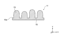
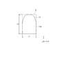
- FIG. 1 is a schematic perspective view of a thin film nanocrystal composite according to the present invention.
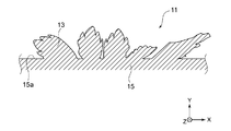
- FIG. 2 is a more detailed schematic perspective view of the thin film nanocrystal composite according to the present invention.
- FIG. 3 is a schematic cross-sectional view showing an II cross section (XY plane) of the schematic perspective view of the thin film nanocrystal composite of FIG.
- FIG. 4 is a more detailed schematic cross-sectional view showing the II cross section (XY plane) of the schematic perspective view of the thin film nanocrystal composite of FIG.
- FIG. 5 is a schematic perspective view showing a region P of the thin film nanocrystal composite in FIG. 1 in an enlarged manner.
- FIG. 6 is a more detailed schematic perspective view showing a region P of the thin film nanocrystal composite of FIG.
- FIG. 7 is a schematic view showing an enlarged view of a nanocrystal piece separated from the thin-film nanocrystal composite shown in FIG. 1 in plan view on the XY plane.
- FIG. 8 is a more detailed schematic view showing a nanocrystal piece separated from the thin film nanocrystal composite of FIG. 2 in an enlarged view in plan view in the XY plane.
- FIG. 9 is an example of an X-ray diffraction spectrum when the structure is analyzed by the nanocrystal composite X-ray diffraction of the present invention.
- FIG. 10 is an observation photograph of the thin-film nanocrystal composite according to Example 1 of the present invention.
- FIG. 11 is an SEM image of the thin film nanocrystal composite according to Example 2 of the present invention.
- FIG. 12 is an SEM image of the powdered nanocrystal piece produced in Comparative Example 1.
- the thin-film nanocrystal composite according to the present invention is formed of a thin-film-like connected assembly in which a plurality of nanocrystal pieces having a main surface and an end face are connected to each other.
- the exposed main surfaces of the plurality of nanocrystal pieces are arranged with a gap, and the connected assembly has a planar view area of 1 mm 2 or more.
- Such a nanocrystal composite is different from conventional nanocrystal materials in the form of powder, and has a macroscopic size of millimeter scale or more by connecting a plurality of nanocrystal pieces to each other. Therefore, in actual use, since it can be used as a thin film-like or sheet-like material, (i) it is possible to selectively cover a portion to be covered of the carrier, and a necessary amount of nanocrystal composite Just prepare. In addition, since (ii) a nanocrystalline composite in the form of a thin film can be attached with an adhesive, for example, when it is assumed to be used as a catalyst, the nanocrystalline composite is formed on a portion (reaction surface) to be supported by a carrier.
- the active surface can be efficiently arranged, and excellent catalytic activity can be realized. Furthermore, (iii) since it is a thin film shape, it is easy to handle and excellent in handling, and (iv) it is easy to clean and isolate after production, and there is no problem such as dissipation, so it can be stored easily.
- FIGS. 1 and 2 show an embodiment of a thin-film nanocrystal composite according to the present invention.
- reference numeral 1 denotes a thin-film nanocrystal composite (hereinafter simply referred to as “nanocrystal composite”). It may be called “body”.)
- 3 and 4 are II sectional views (XY plane) of the thin-film nanocrystal composite 1 shown in FIGS. 1 and 2, respectively.
- 13 is a nanocrystal piece
- 15 is a connecting portion
- 15 a is an exposed portion of the connecting portion 15.
- FIGS. 5 and 6 are schematic perspective views showing an enlarged region P of the thin film nanocrystal composite shown in FIGS. 1 and 2, respectively.
- reference numeral 13 a denotes the main surface of the nanocrystal piece 13
- Reference numeral 13 b denotes an end face of the nanocrystal piece 13.
- the nanocrystal composite 1 of the present invention is in the form of a thin piece, and is a thin film-like connection in which a plurality of nanocrystal pieces having a main surface 13a and an end face 13b are connected to each other. It consists of an assembly 11.
- the connection state of the nanocrystal pieces is not particularly limited, and may be a chemical bond such as crystal growth, an electrical bond such as electrostatic force, or a bond due to accumulation such as intermolecular force.
- the nanocrystal pieces may be connected as a whole to form a thin film aggregate.
- the linked assembly 11 is preferably such that the nanocrystal pieces are linked and integrated by chemical bonding.
- the connection assembly 11 includes a thin-film connection portion 15 having an exposed portion 15 a having a planar view area of 1 mm 2 or more.
- the exposed portion 15a of the connecting portion 15 may be a portion formed by crystal growth of nanocrystal pieces, or may be a portion formed by accumulating nanocrystal pieces.
- Such an exposed part 15a is 1 mm 2 or more in a plan view area, and preferably 100 mm 2 or more.
- the connected assembly 11 having such a millimeter-scale or larger exposed portion 15a is excellent in handleability in actual use.
- assembly 11 is connected to the exposed part 15a of the connection part 15 by each end surface 13b connecting several nanocrystal pieces. , Are arranged at intervals.
- the main surfaces 13a of the plurality of nanocrystal pieces 13 protrude from the exposed portion 15a to the outside of the connection assembly 11, and the main surface 13a is disposed along the surface direction of the thin-film connection portion 15. .
- the main surface 13a protrudes from the exposed portion 15a in a random direction.
- the main surface 13a of the nanocrystal piece 13 faces a random direction.
- Such a linked assembly 11 having a plurality of nanocrystal pieces 13 can exhibit characteristics peculiar to a nanocrystal material while having a size of a millimeter scale or more.
- the connection state of the nanocrystal pieces 13 having the main surface 13 a protruding from the exposed portion 15 a of the connection portion 15 is not particularly limited, and examples thereof include the above-described combined state.
- the nanocrystal pieces 13 are preferably connected to each other by chemical bonding in the connecting portion 15.
- the nanocrystal piece 13 is a part constituting the connected assembly 11 and is in a state where the main surface 13a is connected to the exposed part 15a of the connecting part 15. As shown in FIGS. 5 and 6, such a nanocrystal piece 13 has a thin piece shape and has a main surface 13a and an end face 13b.
- the main surface 13a of the nanocrystal piece 13 is specifically a surface having a large surface area among the outer surfaces constituting the flaky nanocrystal piece 13, and is above and below the end face 13b having a small surface area. It means both surfaces that define the edge.
- the minimum dimension of the main surface 13a of the nanocrystal piece 13 is preferably 1 nm to 2 ⁇ m, and the maximum dimension is preferably 10 nm to 10 ⁇ m. Moreover, it is preferable that the maximum dimension of the end surface of the nanocrystal piece 13 is 1/10 or 10 nm or less of the minimum dimension of the main surface. Moreover, in the nanocrystal piece 13, it is preferable that the ratio of the surface area of the main surface 13a to the end face 13b is 10 times or more in that excellent catalytic activity is obtained, for example, when used as a catalyst. Further, the thickness t of the nanocrystal piece 13 is preferably 0.5 to 100 nm, more preferably 1 to 20 nm. In addition, the minimum dimension of the main surface 13a of the nanocrystal piece 13 is preferably 10 times or more, more preferably 20 times or more of the thickness t in relation to the thickness t.
- the minimum dimension and the maximum dimension of the main surface 13a of the nanocrystal piece 13 measure the nanocrystal piece 13 separated from the connection part 15 as an individual nanocrystal piece so that the shape of the nanocrystal piece 13 is not impaired.
- a rectangle Q having a minimum area that circumscribes the main surface 13a of the nanocrystal piece as the nanocrystal piece 13 is drawn, and the short side L1 and the long side of the rectangle Q are drawn.
- the side L2 is measured as the minimum dimension and the maximum dimension of the nanocrystal piece 13, respectively.
- connection aggregate 11 since the some nanocrystal piece 13 protrudes from the exposed part 15a of the connection part 15, the connection aggregate 11 has a comparatively large specific surface area.
- the specific surface area of such a linked assembly 11 is preferably 5 m 2 / g or more, and more preferably 10 m 2 / g or more.
- the nanocrystal composite 1 composed of such a linked assembly 11 exhibits excellent catalytic activity when used as a catalyst, for example.
- assembly 11 is not specifically limited, The upper limit as a manufacturing or physical limit is 100 m ⁇ 2 > / g, for example.
- the nanocrystal piece constituting the crystal complex 1 of the present invention is preferably constituted of at least one of a metal and a metal oxide.
- the metal include noble metals, transition metals, and alloys containing these metals.
- the noble metal and its alloy are composed of one component selected from the group consisting of palladium (Pd), rhodium (Rh), ruthenium (Ru), platinum (Pt), silver (Ag) and gold (Au). Examples thereof include metals and alloys containing one or more components selected from these groups.
- the transition metal and its alloy are selected from a metal consisting of one component selected from the group of copper (Cu), nickel (Ni), cobalt (Co) and zinc (Zn), or from these groups. Examples include alloys containing one or more components.
- the metal oxide include oxides and composite oxides of noble metals, transition metals, or alloys thereof. Examples of the noble metal and transition metal include those exemplified above.
- the nanocrystal piece is preferably made of a metal oxide containing one or more metals selected from the group of transition metals.
- metal oxides are abundant on the earth as metal resources, and are cheaper than noble metals, and thus are preferable in terms of cost reduction.
- the metal oxide as described above include nickel oxide, copper oxide, Ni—Cu oxide, Cu—Pd oxide, and the like. Among these, copper oxide and Ni—Cu composite oxide are preferable.
- the nanocrystal composite 1 of the present invention is a thin film having a certain size of millimeter order or more, and is an integrated body in which a plurality of nanocrystal pieces are connected to each other. It also exhibits unique properties of nanocrystalline materials. Since such a nanocrystal composite 1 could be handled as a macro thin film of the order of millimeters or more, the nanocrystal material can realize excellent handling properties and workability that are not conventionally provided. On the other hand, it is possible to realize surface properties that could not be realized with conventional metal foils such as electrolytic copper foils, and to exhibit characteristics peculiar to nanocrystalline materials such as nanocrystalline powders while having a thin film shape.
- Such a nanocrystal composite 1 of the present invention can be used for various applications, and can be suitably used as, for example, a catalyst, an electrode material, or an artificial photosynthetic material.
- the nanocrystal composite 1 of the present invention when used as a catalyst, it is not necessary to disperse and embed the nanocrystal composite in an adhesive like a nanocrystal powder when supported on a substrate.
- the active surface can be efficiently arranged on the reaction surface, and the catalyst efficiency is improved.
- the main surface 13a of the nanocrystal piece 13 is an active surface, and thus the main surface 13a of the nanocrystal piece 13 is configured to have a specific crystal orientation. It is preferable.
- a nanocrystal piece is comprised with a metal oxide.
- the main surface 13a of the nanocrystal piece 13 in order to configure the main surface 13a of the nanocrystal piece 13 to be a reducing active surface, in the metal oxide constituting the nanocrystal piece, the surface of the metal atom exhibiting catalytic activity is changed to the main surface.
- the main surface 13a may be composed of a metal atom plane by being oriented so as to be located at 13a. Specifically, the metal atoms occupying the metal atoms and oxygen atoms constituting the metal oxide present on the main surface 13a.
- the number ratio is preferably 80% or more.
- the main surface 13a in order to configure the main surface 13a to be an oxidative active surface, in the metal oxide composing the nanocrystal piece, the surface of the oxygen atom exhibiting catalytic activity is oriented so as to be located on the main surface 13a.
- the main surface 13a may be constituted by an oxygen atom plane.
- the number ratio of oxygen atoms in the metal atoms and oxygen atoms constituting the metal oxide existing on the main surface 13a is 80% or more. It is preferable that
- the main surface 13a is adjusted by adjusting the ratio of the number of metal atoms or oxygen atoms in the metal atoms and oxygen atoms constituting the metal oxide existing on the main surface 13a of the nanocrystal piece 13.
- the catalytic activity function of the nanocrystal 13 can be enhanced, and the nanocrystal piece 13, and thus the nanocrystal composite 1, can exhibit sufficient catalytic activity.
- the main surface 13a of the nanocrystal piece 13 has a specific crystal orientation is that, depending on the type of metal oxide constituting the nanocrystal piece 13, the crystal orientation that exists in the main surface 13a is different. Therefore, the crystal orientation of the main surface 13a is not specifically described.
- the metal oxide is copper oxide (CuO)
- the main crystal orientation of the single crystal constituting the main surface is preferably ⁇ 001 ⁇ .
- the nanocrystal composite 1 has a maximum diffraction angle (2 ⁇ ) of 35.0 to 36.0 degrees in the X-ray diffraction spectrum.
- the peak intensity is I1 and the maximum peak intensity between 38.5 and 40.0 degrees is I2, the peak intensity is preferably I1> I2, more preferably the peak intensity ratio I1 / I2 is 1. It is desirable that the crystal has a degree of crystal orientation that is 0.05 or more, and more preferably has a peak intensity I1 / I2 of 1.2 or more.
- FIG. 9 shows a peak result showing an example of the X-ray diffraction spectrum when the nanocrystal composite 1 of the present invention is subjected to structural analysis by X-ray diffraction. The measurement method will be described on the page of the example.
- the highest peaks I1 and I2 are in the relationship of I1> I2 in terms of peak intensity.
- the highest peak intensity I1 is 35.64 degrees of the crystal plane (002), and the highest peak intensity I2 is It was 39.2 degrees on the (200) plane.
- the maximum peaks I1 and I2 have a peak intensity relationship of I1 ⁇ I2
- the maximum peak intensity I1 is 35.76 degrees of the crystal plane ( ⁇ 111) and the maximum peak intensity I2 is (111). ) Plane of 38.96 degrees.
- the main surface 13a has a metal atomic plane.
- the metal oxide crystal structure is a regular structure in which metal atomic planes and oxygen atomic planes are regularly and alternately stacked, and the arrangement of atoms is regular.
- the main surface 13a is preferably configured such that the metal atomic plane is located.
- the main surface 13a is different not only in the case of a structure composed of an aggregate of single crystals having the same orientation, but is different. Even a structure composed of single crystal aggregates having different crystal structures or different orientations or aggregates including crystal grain boundaries and polycrystals is included when the metal surface is present on the main surface 13a.
- Examples of the method for producing the thin film nanocrystal composite of the present invention include a method for preferentially causing two-dimensional growth of nanocrystal pieces.
- a boundary surface in contact with a boundary where different phases exist such as a gas and a solution, is used as a nucleation priority place. That is, for example, a nanocrystal complex is formed as a thin film on the interface between a gas and a solution, an interface between different types of liquids, or an interface with a substrate (support) placed in the solution.
- a nucleation place is limited and it grows two-dimensionally, it is desirable to manufacture at a temperature lower than a normal hydrothermal method.
- the material of the support base is not particularly limited, and examples thereof include metals, oxides, nitrides, and the like. From the viewpoint of supporting a thin film, Teflon (registered trademark) having excellent chemical resistance at temperatures up to 200 degrees. ) Is desirable.
- Example 1 After mixing 2.0 g of copper chloride (II) dihydrate (manufactured by Junsei Chemical Co., Ltd.) and 1.6 g of urea (manufactured by Junsei Chemical Co., Ltd.), 180 ml of ethylene glycol (manufactured by Junsei Chemical Co., Ltd.) ) And 120 ml of water were added and further mixed. The obtained mixed solution of copper chloride and urea was poured into a pressure resistant glass container having an internal volume of 500 ml, and heat treatment was performed at 150 ° C. for 12 hours in a sealed atmosphere inside the container.
- copper chloride (II) dihydrate manufactured by Junsei Chemical Co., Ltd.
- urea manufactured by Junsei Chemical Co., Ltd.
- 120 ml of water were added and further mixed.
- the obtained mixed solution of copper chloride and urea was poured into a pressure resistant glass container having an internal volume of 500 ml, and heat treatment was performed at 150
- the mixed solution is cooled to room temperature and kept for 1 day, and further, a thin film-shaped precipitate formed from the sealed container is recovered, and this precipitate is washed with methanol and pure water, and is subjected to 70% under vacuum.
- the nanocrystal copper oxide catalyst which consists of the thin film-like connection aggregate
- Example 2 After mixing 1.4 g of copper (II) chloride dihydrate (same as above) and 1.0 g of urea (same as above), 108 ml of ethylene glycol (same as above) and 72 ml of water were added and further mixed.
- the obtained mixed solution of copper chloride and urea was poured into an SUS autoclave hermetically sealed container having an internal volume of 300 ml, and heat treatment was performed in the container at 150 ° C. for 24 hours. Thereafter, the mixed solution is cooled to room temperature and kept for 1 day, and further, a thin film-shaped precipitate formed from the sealed container is recovered, and this precipitate is washed with methanol and pure water, and is subjected to 70% under vacuum.
- the nanocrystal copper oxide catalyst which consists of the thin film-like connection aggregate
- Comparative Example 2 As Comparative Example 2, commercially available copper oxide nanoparticles (544868 Copper (II) oxide manufactured by Sigma Aldrich Japan GK) were prepared and used as a nanocrystalline copper oxide catalyst composed of spherical nanocrystal grains of copper oxide.
- FIG. 10A is an external photograph of a nanocrystalline copper oxide catalyst (area of about 255 mm 2 and weight of 20.06 g) made of a thin film-like connected assembly produced in Example 1, and FIG.
- FIG. 11 is an SEM image at a magnification of 30,000 of the nanocrystalline copper oxide catalyst composed of the thin film-like connected assembly produced in Example 2.
- FIG. 12 is an SEM image when the nanocrystalline copper oxide catalyst composed of powdered nanocrystal pieces prepared in Comparative Example 1 is observed at a magnification of 50,000 times.
- the planar view area of the connecting portion of the connected assembly was calculated by identifying the outline of the connected assembly in the appearance photograph taken from the vertical direction with respect to the surface of the connected assembly, and analyzing the image.
- the thickness and minimum dimensions of the nanocrystal pieces and powdered nanocrystal pieces constituting the linked aggregate, and the particle size of the powdered spherical nanocrystal grains are measured by analyzing SEM images at a magnification of 50,000 times. did.
- the thickness and minimum dimension of the nanocrystal piece were calculated by individualizing the nanocrystal piece so as not to break the shape, observing the individualized nanocrystal piece at the above magnification, and analyzing the SEM image.
- the thickness and minimum dimensions of the nanocrystal pieces and powdered nanocrystal pieces constituting the linked assembly, and the particle size of the powdered spherical nanocrystal grains were arbitrarily selected from 10 nanocrystal pieces and nanocrystal pieces. The value measured and averaged for the crystal grains.
- the take-out rate was 90% or more as an acceptable level.
- Catalyst performance Evaluation of catalyst performance was performed using an apparatus including a gas supply line, a reaction tube, and a gas sampling unit. Specifically, it is as follows. First, 20 mg of the catalyst was charged between the glass filters of the reaction tube. Next, the reaction tube filled with the catalyst was set in the apparatus, and the thermostatic chamber containing the reaction tube was heated from room temperature to 200 ° C. at 10 ° C./min. At this time, reaction tube inlet gas (raw material gas) and reaction tube outlet gas were sampled and subjected to gas analysis to calculate NO conversion rate and CO conversion rate. In addition, the mixed gas of carbon monoxide and nitric oxide (Ar: CO: NO is 98: 1: 1 by mass ratio) was used for source gas.
- the flow rate of the raw material gas is such that the flow rate of each gas (Ar, CO and NO) is measured with a float type flow meter and adjusted with a secondary pressure fluctuation type flow controller valve so that the flow rate of the mixed gas becomes 50 mL / min. Adjusted.
- the material of the reaction tube was quartz glass, and a SUS tube was connected for preheating of the gas supplied to the reaction tube.
- the reaction tube inlet gas and the reaction tube outlet gas were collected from the outlets of the four-way valve and the three-way valve with a 1 L aluminum bag for 20 minutes.
- the collected gas was analyzed using a gas chromatograph (GC-8A, manufactured by Shimadzu Corporation) for nitrogen (N 2 ), nitric oxide (NO), and carbon monoxide (CO), and carbon dioxide (CO 2 ).
- a gas chromatograph (GC-2010, manufactured by Shimadzu Corporation) was used. Further, the NO conversion rate and the CO conversion rate can be calculated from the following formulas (1) from the amounts (ppm) of nitrogen, nitrogen monoxide, carbon monoxide and carbon dioxide in the respective gases collected at the inlet and outlet of the reaction tube. ) And (2).
- NO conversion rate (%) ⁇ N 2 (outlet) ⁇ N 2 (inlet) ⁇ ⁇ 100 / NO (inlet) (1)
- CO conversion rate (%) CO 2 (outlet) ⁇ 100 / CO (raw material gas) (2)
- NO conversion rate and the CO conversion rate were each evaluated as good when 50% or more.
- FIG. 10C and FIG. 11 in Examples 1 and 2, the main surfaces of the plurality of nanocrystal pieces protrude from the exposed portion, and the main surfaces extend along the surface direction of the thin film-like connecting portion. Since it is arranged, it was confirmed to be a thin film-like connected assembly having a certain continuity (Note that FIGS. 10 (a) and (b) are those of Example 1, A similar thin film-like connected assembly was also observed in Example 2). Therefore, in Examples 1 and 2, it was confirmed that it was not a powder of nanocrystal pieces.
- Such a thin-film nanocrystal composite of the present invention adheres to a container or the like to some extent due to the influence of static electricity, but can be collected with tweezers and does not collapse by sampling, and has strength to support its own weight. confirmed.
- the thin film-like crystal composite of the present invention exhibits excellent balanced characteristics in all items of handling property, dissipation resistance and catalyst performance, particularly when used as a catalyst. It has been confirmed that it works.
- the catalyst comprising the thin film nanocrystal composite of the present invention did not change in shape or the like before and after the catalytic reaction, and the stability against the catalytic reaction was also confirmed.
- the catalyst of Comparative Example 1 is configured such that the main surfaces of the plurality of nanocrystal pieces do not protrude from the exposed portion and the powdery nanocrystal pieces are aggregated. It was confirmed that In particular, since the catalyst of Comparative Example 1 is in the form of a powder, there is no continuity between the nanocrystal pieces, and it is impossible to collect in a collective state such as pinching with tweezers. It was confirmed that the film was inferior in terms of handleability compared to the thin film nanocrystal composites of the present invention (Examples 1 and 2), such as scattering and adhesion to containers and the like, which were easily lost. In addition, the catalyst which consists of a powdery nanocrystal piece of the comparative example 1 also did not change the shape etc. before and after the catalytic reaction, and the stability against the catalytic reaction was confirmed.
- the catalyst of Comparative Example 2 is composed of powdered spherical nanocrystal grains. For this reason, in particular, since it is in the form of a powder, it is impossible to collect in a collective state such as pinching with tweezers, as in the case of the nanocrystal piece of Comparative Example 1. It was confirmed that the film was inferior in terms of handleability compared to the thin film nanocrystal composites of the present invention (Examples 1 and 2), such as adhesion to a container and the like, which was easily lost.
- the catalysts of Comparative Examples 1 and 2 are in powder form, they are inferior to the thin film nanocrystal composites of the present invention (Examples 1 and 2) from the viewpoint of dissipation resistance and removal rate. It was confirmed that Furthermore, the catalysts of Comparative Examples 1 and 2 were significantly inferior to the thin-film nanocrystal composites of the present invention (Examples 1 and 2) in terms of NO conversion ratio among the catalyst performances. Further, the catalyst of Comparative Example 2 was inferior to Examples 1 and 2 not only in NO conversion rate but also in CO conversion rate. Further, in the catalyst of Comparative Example 2, the powder was dissipated and partially changed to copper before and after the catalytic reaction, and in particular, the dissipating property and the instability to the catalytic reaction were confirmed.
Landscapes
- Chemical & Material Sciences (AREA)
- Engineering & Computer Science (AREA)
- Organic Chemistry (AREA)
- Chemical Kinetics & Catalysis (AREA)
- Materials Engineering (AREA)
- Environmental & Geological Engineering (AREA)
- Oil, Petroleum & Natural Gas (AREA)
- Biomedical Technology (AREA)
- Health & Medical Sciences (AREA)
- Inorganic Chemistry (AREA)
- General Chemical & Material Sciences (AREA)
- Analytical Chemistry (AREA)
- Physics & Mathematics (AREA)
- Combustion & Propulsion (AREA)
- Thermal Sciences (AREA)
- Catalysts (AREA)
- Crystallography & Structural Chemistry (AREA)
Abstract
La présente invention concerne un complexe nanocristallin de type film mince grâce auquel il est désormais possible de pallier les problèmes mentionnés ci-dessus d'un matériau nanocristallin ayant une forme poudreuse tout en conservant les propriétés d'un matériau nanocristallin (par exemple, une excellente activité catalytique) de manière satisfaisante, et qui présente d'excellentes propriétés de manipulation et peut être utilisé en tant que matériau nanocristallin. Un complexe nanocristallin de type film mince qui est composé d'un ensemble connecté de type film mince dans lequel de multiples éléments de nanocristal ayant chacun une forme de type film mince et ayant une surface principale et une surface de bord qui sont reliées l'une à l'autre, ledit complexe nanocristallin étant caractérisé en ce que les surfaces principales des multiples éléments de nanocristal qui sont exposés à l'extérieur de l'ensemble relié sont agencés de façon à former des espaces entre eux, et l'ensemble relié a une surface en vue plane supérieure ou égale à 1 mm2.
Priority Applications (4)
| Application Number | Priority Date | Filing Date | Title |
|---|---|---|---|
| CN201880003095.9A CN109562954B (zh) | 2017-03-07 | 2018-03-07 | 薄膜状纳米晶体复合体 |
| EP18763816.8A EP3594180A4 (fr) | 2017-03-07 | 2018-03-07 | Complexe nanocristallin de type film mince |
| JP2019504626A JP7060574B2 (ja) | 2017-03-07 | 2018-03-07 | 薄膜状ナノ結晶複合体 |
| US16/563,180 US11958756B2 (en) | 2017-03-07 | 2019-09-06 | Thin-film-like composite of nanocrystal |
Applications Claiming Priority (2)
| Application Number | Priority Date | Filing Date | Title |
|---|---|---|---|
| JP2017043204 | 2017-03-07 | ||
| JP2017-043204 | 2017-03-07 |
Related Child Applications (1)
| Application Number | Title | Priority Date | Filing Date |
|---|---|---|---|
| US16/563,180 Continuation US11958756B2 (en) | 2017-03-07 | 2019-09-06 | Thin-film-like composite of nanocrystal |
Publications (1)
| Publication Number | Publication Date |
|---|---|
| WO2018164163A1 true WO2018164163A1 (fr) | 2018-09-13 |
Family
ID=63447640
Family Applications (1)
| Application Number | Title | Priority Date | Filing Date |
|---|---|---|---|
| PCT/JP2018/008689 WO2018164163A1 (fr) | 2017-03-07 | 2018-03-07 | Complexe nanocristallin de type film mince |
Country Status (5)
| Country | Link |
|---|---|
| US (1) | US11958756B2 (fr) |
| EP (1) | EP3594180A4 (fr) |
| JP (1) | JP7060574B2 (fr) |
| CN (1) | CN109562954B (fr) |
| WO (1) | WO2018164163A1 (fr) |
Cited By (2)
| Publication number | Priority date | Publication date | Assignee | Title |
|---|---|---|---|---|
| WO2020162336A1 (fr) * | 2019-02-06 | 2020-08-13 | 古河電気工業株式会社 | Complexe nanocristallin |
| EP3778470A4 (fr) * | 2018-03-27 | 2021-12-22 | Furukawa Electric Co., Ltd. | Complexe de commande d'orientation de cristal |
Citations (7)
| Publication number | Priority date | Publication date | Assignee | Title |
|---|---|---|---|---|
| US20130089739A1 (en) * | 2011-10-07 | 2013-04-11 | King Abdullah University of Science and Technology (KAUST) | Nanostructured metal oxides and mixed metal oxides, methods of making these nanoparticles, and methods of their use |
| WO2013133412A1 (fr) * | 2012-03-08 | 2013-09-12 | 堺化学工業株式会社 | Particules sphériques d'oxyde de zinc formées d'oxyde de zinc lamellaire agrégé, leur procédé de préparation, produit cosmétique et charge de dissipation de chaleur |
| JP2013240756A (ja) | 2012-05-21 | 2013-12-05 | National Institute For Materials Science | ナノ単結晶板材集積触媒及びその製造方法 |
| CN103708551A (zh) * | 2013-12-26 | 2014-04-09 | 湛江师范学院 | 一种乙二醇-水混合溶剂热合成碳酸氧铋花状微球的制备方法 |
| JP2016011247A (ja) * | 2014-06-03 | 2016-01-21 | 株式会社豊田中央研究所 | 板状リン酸化合物粒子、それを含む板状リン酸化合物粉体、及び、板状リン酸化合物粉体の製造方法、並びに板状リン酸化合物粉体を用いた結晶配向アパタイトの製造方法 |
| WO2017010491A1 (fr) * | 2015-07-15 | 2017-01-19 | 古河電気工業株式会社 | Catalyseur de complexe nano-cristallin pour le stockage/la fourniture d'hydrogène, mélange de catalyseur de complexe nano-cristallin pour le stockage/la fourniture d'hydrogène et procédé de fourniture d'hydrogène |
| WO2017010492A1 (fr) * | 2015-07-15 | 2017-01-19 | 古河電気工業株式会社 | Catalyseur intégré à un substrat comprenant un complexe d'oxyde métallique nanocristallin, procédé de production associé, et composant de catalyseur |
Family Cites Families (1)
| Publication number | Priority date | Publication date | Assignee | Title |
|---|---|---|---|---|
| CN104176763B (zh) * | 2014-07-22 | 2017-04-05 | 惠州学院 | 一种特殊结构纳米氧化铜薄膜及其制备方法和应用 |
-
2018
- 2018-03-07 JP JP2019504626A patent/JP7060574B2/ja active Active
- 2018-03-07 CN CN201880003095.9A patent/CN109562954B/zh active Active
- 2018-03-07 EP EP18763816.8A patent/EP3594180A4/fr active Pending
- 2018-03-07 WO PCT/JP2018/008689 patent/WO2018164163A1/fr unknown
-
2019
- 2019-09-06 US US16/563,180 patent/US11958756B2/en active Active
Patent Citations (7)
| Publication number | Priority date | Publication date | Assignee | Title |
|---|---|---|---|---|
| US20130089739A1 (en) * | 2011-10-07 | 2013-04-11 | King Abdullah University of Science and Technology (KAUST) | Nanostructured metal oxides and mixed metal oxides, methods of making these nanoparticles, and methods of their use |
| WO2013133412A1 (fr) * | 2012-03-08 | 2013-09-12 | 堺化学工業株式会社 | Particules sphériques d'oxyde de zinc formées d'oxyde de zinc lamellaire agrégé, leur procédé de préparation, produit cosmétique et charge de dissipation de chaleur |
| JP2013240756A (ja) | 2012-05-21 | 2013-12-05 | National Institute For Materials Science | ナノ単結晶板材集積触媒及びその製造方法 |
| CN103708551A (zh) * | 2013-12-26 | 2014-04-09 | 湛江师范学院 | 一种乙二醇-水混合溶剂热合成碳酸氧铋花状微球的制备方法 |
| JP2016011247A (ja) * | 2014-06-03 | 2016-01-21 | 株式会社豊田中央研究所 | 板状リン酸化合物粒子、それを含む板状リン酸化合物粉体、及び、板状リン酸化合物粉体の製造方法、並びに板状リン酸化合物粉体を用いた結晶配向アパタイトの製造方法 |
| WO2017010491A1 (fr) * | 2015-07-15 | 2017-01-19 | 古河電気工業株式会社 | Catalyseur de complexe nano-cristallin pour le stockage/la fourniture d'hydrogène, mélange de catalyseur de complexe nano-cristallin pour le stockage/la fourniture d'hydrogène et procédé de fourniture d'hydrogène |
| WO2017010492A1 (fr) * | 2015-07-15 | 2017-01-19 | 古河電気工業株式会社 | Catalyseur intégré à un substrat comprenant un complexe d'oxyde métallique nanocristallin, procédé de production associé, et composant de catalyseur |
Non-Patent Citations (4)
| Title |
|---|
| KHUN, K. ET AL.: "Urea Assisted Synthesis of Flower Like CuO Nanostructures and Their Chemical Sensing Application for the Determination of Cadmium Ions", ELECTROANALYSIS, vol. 25, no. 6, 1 June 2013 (2013-06-01), pages 1425 - 1432, XP009516660, ISSN: 1040-0397 * |
| See also references of EP3594180A4 |
| VASEEM, M. ET AL.: "Flower-shaped CuO nanostructures: structral, photocatalytic and XANES studies", CATALYSIS COMMUNICATIONS, vol. 10, no. 1, 29 July 2008 (2008-07-29), pages 11 - 16, XP025479496, ISSN: 1566-7367, DOI: 10.1016/j.catcom.2008.07.022 * |
| ZHU, LU-PING ET AL.: "Self-assembled 3D flower-like hierarchical beta-Ni(OH)2 hollow architectures and their in situ thermal Conversion to NiO", NANOSCALE RESEARCH LETTERS, vol. 4, 27 February 2009 (2009-02-27), pages 550 - 557, XP055348433, ISSN: 1931-7573, DOI: 10.1007/s11671-009-9279-9 * |
Cited By (3)
| Publication number | Priority date | Publication date | Assignee | Title |
|---|---|---|---|---|
| EP3778470A4 (fr) * | 2018-03-27 | 2021-12-22 | Furukawa Electric Co., Ltd. | Complexe de commande d'orientation de cristal |
| WO2020162336A1 (fr) * | 2019-02-06 | 2020-08-13 | 古河電気工業株式会社 | Complexe nanocristallin |
| CN112512686A (zh) * | 2019-02-06 | 2021-03-16 | 古河电气工业株式会社 | 纳米晶体复合体 |
Also Published As
| Publication number | Publication date |
|---|---|
| EP3594180A4 (fr) | 2021-01-13 |
| CN109562954A (zh) | 2019-04-02 |
| JPWO2018164163A1 (ja) | 2020-01-09 |
| CN109562954B (zh) | 2022-12-06 |
| JP7060574B2 (ja) | 2022-04-26 |
| US11958756B2 (en) | 2024-04-16 |
| US20200017367A1 (en) | 2020-01-16 |
| EP3594180A1 (fr) | 2020-01-15 |
Similar Documents
| Publication | Publication Date | Title |
|---|---|---|
| Gupta et al. | A low temperature hydrogen sensor based on palladium nanoparticles | |
| Yang et al. | Shape-controlled synthesis of palladium and copper superlattice nanowires for high-stability hydrogen sensors | |
| Ding et al. | Catalyst− nanostructure interfacial lattice mismatch in determining the shape of VLS grown nanowires and nanobelts: a case of Sn/ZnO | |
| JP4728093B2 (ja) | 固/液界面に形成された吸着ミセル膜を反応場として形成される単結晶質の貴金属超薄膜ナノ粒子及びその製造方法 | |
| Fang et al. | External electric field driven 3D ordering architecture of silver (I) oxide meso-superstructures | |
| JP6757726B2 (ja) | 基材一体型ナノ結晶金属酸化物複合体含有触媒およびその製造方法ならびに触媒部品 | |
| Kim et al. | Novel growth of CuO-functionalized, branched SnO2 nanowires and their application to H2S sensors | |
| Sow et al. | Noble metal nanomaterials with nontraditional crystal structures | |
| Shaalan et al. | Synthesis of metal and metal oxide nanostructures and their application for gas sensing | |
| WO2018164163A1 (fr) | Complexe nanocristallin de type film mince | |
| Qin et al. | Hierarchical layered double hydroxides with Ag nanoparticle modification for ethanol sensing | |
| Sengar et al. | Size and alloying induced changes in lattice constant, core, and valance band binding energy in Pd-Ag, Pd, and Ag nanoparticles: Effect of in-flight sintering temperature | |
| US10584030B2 (en) | Nanocrystalline composite catalyst for storing/supplying hydrogen, nanocrystalline composite catalyst mixture for storing/supplying hydrogen, and method for supplying hydrogen | |
| Jiang et al. | An in situ electrospinning route to fabricate NiO–SnO2 based detectors for fast H2S sensing | |
| JP4958109B2 (ja) | ナノホールを有するシート状白金ナノ粒子及びその製造法 | |
| Kong et al. | Nanocube-aggregated cauliflower-like copper hierarchical architectures: synthesis, growth mechanism and electrocatalytic activity | |
| Li et al. | Ultrasound-assisted preparation, characterization and properties of porous Cu 2 O microcubes | |
| WO2019189032A1 (fr) | Complexe de commande d'orientation de cristal | |
| Khare et al. | Synthesis of WO3 nanoblades by the dealloying of glancing angle deposited W-Fe nanocolumnar thin films | |
| WO2020162336A1 (fr) | Complexe nanocristallin | |
| Chu et al. | Size-tunable Au nanoparticles on MoS2 (0001) | |
| JP6762520B2 (ja) | ナノ粒子の製造方法 | |
| Shen et al. | Growth and aggregation of Cu nanocrystals on ionic liquid surfaces | |
| Ding et al. | Self-feeding formation of atomically thin molybdenum nanoflakes on MoS2 monolayer | |
| Hoa et al. | Self-Catalytic Growth of TiO2− δ Nanobelts and Nanosheets Using Metallorganic Chemical Vapor Deposition |
Legal Events
| Date | Code | Title | Description |
|---|---|---|---|
| 121 | Ep: the epo has been informed by wipo that ep was designated in this application |
Ref document number: 18763816 Country of ref document: EP Kind code of ref document: A1 |
|
| ENP | Entry into the national phase |
Ref document number: 2019504626 Country of ref document: JP Kind code of ref document: A |
|
| NENP | Non-entry into the national phase |
Ref country code: DE |
|
| ENP | Entry into the national phase |
Ref document number: 2018763816 Country of ref document: EP Effective date: 20191007 |