WO2018163576A1 - 誘導結合プラズマ質量分析装置用プラズマコーン、誘導結合プラズマ質量分析装置、誘導結合プラズマ質量分析装置用プラズマコーンの製造方法 - Google Patents
誘導結合プラズマ質量分析装置用プラズマコーン、誘導結合プラズマ質量分析装置、誘導結合プラズマ質量分析装置用プラズマコーンの製造方法 Download PDFInfo
- Publication number
- WO2018163576A1 WO2018163576A1 PCT/JP2017/046971 JP2017046971W WO2018163576A1 WO 2018163576 A1 WO2018163576 A1 WO 2018163576A1 JP 2017046971 W JP2017046971 W JP 2017046971W WO 2018163576 A1 WO2018163576 A1 WO 2018163576A1
- Authority
- WO
- WIPO (PCT)
- Prior art keywords
- plasma
- cone
- mass spectrometer
- inductively coupled
- platinum
- Prior art date
- Legal status (The legal status is an assumption and is not a legal conclusion. Google has not performed a legal analysis and makes no representation as to the accuracy of the status listed.)
- Ceased
Links
Images




Classifications
-
- H—ELECTRICITY
- H01—ELECTRIC ELEMENTS
- H01J—ELECTRIC DISCHARGE TUBES OR DISCHARGE LAMPS
- H01J49/00—Particle spectrometers or separator tubes
- H01J49/02—Details
- H01J49/06—Electron- or ion-optical arrangements
-
- H—ELECTRICITY
- H01—ELECTRIC ELEMENTS
- H01J—ELECTRIC DISCHARGE TUBES OR DISCHARGE LAMPS
- H01J49/00—Particle spectrometers or separator tubes
- H01J49/02—Details
- H01J49/10—Ion sources; Ion guns
Definitions
- the present invention relates to a plasma cone used for an interface unit of an inductively coupled plasma mass spectrometer, an inductively coupled plasma mass spectrometer equipped with the same, and a method for manufacturing the plasma cone.
- ICPMS inductively coupled plasma mass spectrometer
- ICPMS is a sample introduction unit that introduces sample solution by spraying, a plasma torch unit that ionizes elements contained in the sprayed sample, an interface unit that takes ions into a vacuum system with a mass spectrometer, and mass analysis of ions efficiently
- the interface part is composed of two types of plasma cones (sampling cone and skimmer cone) with a small hole in the center, good thermal conductivity, strong and high corrosion resistance, and the material is nickel or copper. In some cases, platinum is used only at the tip (see FIG. 4).
- Patent Document 1 discloses that the entire plasma cone is formed of platinum.
- Platinum is a metal with good thermal conductivity, strong and high corrosion resistance. If the plasma cone is made of platinum, the background rise of nickel, copper, etc. can be suppressed, and the life is longer than the plasma cone of nickel or copper. It seems to extend. However, it has been found that there is a problem that the sensitivity (ionic strength) is inferior to that of a nickel or copper plasma cone. ICPMS is a device characterized by high sensitivity analysis, but poor sensitivity is undesirable at the expense of device performance.
- the present invention has been made in view of the above problems, and a plasma cone capable of reducing impurity background without sacrificing sensitivity (ion strength) and further improving durability, and an inductively coupled plasma mass provided with the plasma cone It is an object of the present invention to provide an analyzer and a method for manufacturing the plasma cone.
- the plasma cone for an inductively coupled plasma mass spectrometer of the present invention is characterized in that it has a coating film of platinum or a platinum group metal other than platinum or gold or an alloy thereof on the surface.
- the inductively coupled plasma mass spectrometer of the present invention includes a plasma cone having a coating film of platinum or a platinum group metal other than platinum, gold, or an alloy thereof on the surface.
- platinum group metals other than platinum are ruthenium, rhodium, palladium, osmium, or iridium.
- the coating film is preferably formed of platinum.
- the coating film is preferably formed by an ion plating method or a plasma CVD method. According to this, compared with the case where methods other than ion plating method and plasma CVD method are used, a high quality coating film can be formed.
- FIG. 1 It is a block diagram of an inductively coupled plasma mass spectrometer. It is sectional drawing of the plasma torch part and interface part (sampling cone, skimmer cone) of an inductively coupled plasma mass spectrometer. It is a side view of the sampling cone of an Example. It is a side view of the skimmer cone of an Example. It is a side view of the sampling cone of the comparative example 1. 6 is a side view of a skimmer cone of Comparative Example 1. FIG. It is a side view of the sampling cone of the comparative example 2. 6 is a side view of a skimmer cone of Comparative Example 2. FIG.
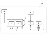
- FIG. 1 shows the configuration of the ICPMS 100 of this embodiment.
- the sample solution 1 is introduced as a spray into the introduction part 2, gasified there, and introduced into the plasma of the plasma torch part 4 by a carrier gas 3 such as argon gas.
- argon gas 5 is introduced into the plasma torch unit 4, and argon plasma is generated when electric power is applied from the high frequency power source 6.
- the gasified sample is heated to, for example, 8000 to 10000 K in this plasma and ionized.
- the ionized sample passes through the interface unit 7 composed of two kinds of plasma cones of the sampling cone 14 and the skimmer cone 16 shown in FIG. 2 and is kept in the vacuum chamber 8 maintained at a high vacuum by the differential exhaust 9.
- the ions introduced into the vacuum chamber 8 are focused by the ion lens unit 10 and then mass-separated and detected by the mass spectrometer 11.
- Data (mass spectrum) detected by the mass spectrometer 11 is sent to the arithmetic device 12, and analysis processing is performed by the arithmetic device 12.
- each of the sampling cone 14 and the skimmer cone 16 shown in FIG. 2 has a cone shape (conical shape), and small-diameter holes 143 and 163 (orifices) are formed at the tips thereof. These holes 143 and 163 are arranged at positions facing the plasma from the plasma torch part 4. Note that the sampling cone 14 and the skimmer cone 16 are arranged in this order as viewed from the plasma torch unit 4. The sample ionized by the plasma torch unit 4 passes through the central holes 143 and 163 of the sampling cone 14 and the skimmer cone 16 and is introduced into the vacuum chamber 8 in the form of a beam.
- the sampling cone 14 and the skimmer cone 16 are each formed of a base material 141, 161 formed in a cone shape, and a coating film formed on the surface of the base material 141, 161 (the outer surface facing the plasma torch part 4 side). 142, 162.
- Base materials 141 and 161 are made of a metal other than platinum group metal, gold, or an alloy thereof except at least the tip, and specifically, for example, copper, nickel, aluminum, or the like.
- the tips of the base materials 141 and 161 may also be formed of a metal other than platinum group metal, gold, or an alloy thereof (copper, nickel, aluminum, etc.), or may be made of a platinum group metal, gold, or an alloy thereof. It may be formed.
- the coating films 142 and 162 are formed of a platinum group metal or gold or an alloy thereof having excellent corrosion resistance compared to copper, nickel, or the like, but is preferably formed of platinum having particularly excellent corrosion resistance.
- the coating films 142 and 162 are formed so as to cover the entire outer surfaces of the base materials 141 and 161.
- the coating films 142 and 162 may not be formed on the inner surfaces (rear surfaces) of the base materials 141 and 161, or may be formed.
- the coating films 142 and 162 are preferably formed by an ion plating method or a plasma CVD (Chemical Vapor Deposition) method. According to this, high-quality coating films 142 and 162 can be obtained as shown in the examples described later.
- the coating films 142 and 162 of platinum group metal, gold, or their alloys are sacrificed as shown in examples described later.
- sensitivity ionic strength
- the impurity background can be lowered and the durability of the plasma cones 14 and 16 can be improved.
- Example 1 As an apparatus for evaluation, a high-resolution inductively coupled plasma mass spectrometer ELEMENT 2 manufactured by Thermo Fisher Scientific Co., Ltd. was used, and the plasma cones of FIGS. Comparison was made between the ion intensity, the ion intensity ratio, and the detection lower limit value when using the comparative example 2) and the plasma cones (Examples) of FIGS. 3A and 3B.
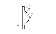
- the plasma cone (sampling cone 24, skimmer cone 25) of FIG. 4A and FIG. 4B has a nickel (Ni) plating 21 on the surface of the copper (Cu) base material 20, and further,
- the structure has a platinum (Pt) chip 22 at the tip.
- the plasma cones (sampling cone 26 and skimmer cone 27) in FIGS. 5A and 5B are all formed of platinum 28.
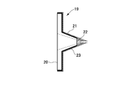
- 3A and 3B (sampling cone 18 and skimmer cone 19) is formed by depositing a platinum coating film 23 on the surface of the plasma cones 24 and 25 of FIGS. 4A and 4B by an ion plating method to 20 ⁇ m. Structure. 3A, FIG. 3B, FIG. 4A, and FIG. 4B, the tip platinum tip 22 is indicated by hatching.
- a blank solution obtained by diluting ultra high purity nitric acid (TAMAPURE-AA-100) made by Tama Chemical with ultrapure water to 5 wt% (weight%), and In, Na, Mg, Al, Ca, Cr, Na and Mg in the plasma cones 18, 19, 24, 25, 26 and 27 of FIGS. 3 to 5 are prepared using a standard solution prepared so that each concentration of Fe, Ni, Cu and Zn is 0.1 ppb.
- the background ionic strength of Al, Ca, Cr, Fe, Ni, Cu, and Zn and the ionic strength of In were compared. The results are shown in Table 1.
- the background ionic strength of Na, Mg, Al, Ca, Cr, Fe, Ni, Cu, and Zn shows the result in the blank solution
- the ionic strength of In is the result in the standard solution with In of 0.1 ppb. Is shown.
- the result of Table 1 has performed the ionic strength measurement using the blank solution and the standard solution several times, respectively, and has shown the average value of the obtained several times of measurement results.
- the In ion intensity is substantially the same as that of the plasma cones 24 and 25 of the comparative example 1 of FIGS. 4A and 4B.
- the ionic strength background ionic strength
- the surface of the base material 20 is covered with the platinum 23, so that it is considered that the evaporation of the elements due to the base material 20 could be prevented.
- the ionic strength ratio of each element to the In strength is also reduced (see Table 2), and the detection lower limit is also improved (see Table 3).
- the background ion intensity is reduced compared to the plasma cones 24 and 25 of the comparative example 1 of FIGS. 4A and 4B.
- the ionic strength of each element has decreased to about 1/20 (see Table 1), the ratio of the ionic strength of each element to the In intensity has increased conversely (see Table 2), and the detection lower limit has also deteriorated. (See Table 3).
- Example 2 To the base material of each platinum film when the platinum film on the surface of the plasma cone is formed by various coating methods (specifically, ion plating method, vacuum deposition method, sputter deposition method, plasma CVD method, electroplating method) The degree of impurity contamination during film formation was investigated.
- the structure of the base material of the plasma cone is the structure shown in FIGS. 4A and 4B (the structure having the nickel plating 21 on the surface of the copper base material 20 and the platinum tip 22 at the tip).
- the survey results are shown in Table 4.
- the adhesion is slightly inferior to that in the case of using the ion plating method ( ⁇ ), but the film density and the degree of impurity contamination during film formation are good ( ⁇ ). It can be seen that the CVD method is also preferable as a coating method for the platinum film.
- Example 3 (Example 3) 3A and 3B (contained by depositing 20 ⁇ m of platinum 23 on the plasma cones 24 and 25 of FIGS. 4A and 4B) and the plasma cones 24 and 25 of FIGS. 4A and 4B (copper base material)
- the durability (life) of each of the plasma cones) having nickel plating 21 on the surface 20 and platinum tip 22 at the tip was investigated. The results are shown in Table 5.
- the durability of the conventional plasma cone was about 3 months, whereas the plasma cone having a platinum coating (FIG. 3A).
- the durability of the plasma cones 18 and 19) in FIG. 3B was 6 to 8 months, which was approximately twice that of the conventional plasma cone.
- the durability of the plasma cone can be improved by coating the surface with platinum, which is superior in corrosion resistance compared to copper and nickel.
- 3A and 3B show a structure in which a platinum coating film 23 is formed on the surfaces of the plasma cones 24 and 25 of FIGS. 4A and 4B as an embodiment of the present invention. However, the plasma of FIGS. 5A and 5B is shown.
- a structure in which a coating film of a platinum group metal or gold or an alloy thereof is formed on the surfaces of the cones 26 and 27 (that is, a structure in which the entire base material is formed of platinum and a coating film is formed on the surface of the platinum base material) ) May be adopted. This also achieves the same sensitivity as when the plasma cones 26 and 27 of FIGS. 5A and 5B are used, while reducing the impurity background caused by the platinum base material and further improving the durability.
Landscapes
- Chemical & Material Sciences (AREA)
- Analytical Chemistry (AREA)
- Physics & Mathematics (AREA)
- Engineering & Computer Science (AREA)
- Plasma & Fusion (AREA)
- Other Investigation Or Analysis Of Materials By Electrical Means (AREA)
- Electron Tubes For Measurement (AREA)
Abstract
誘導結合プラズマ質量分析装置のインターフェース部を構成するプラズマコーンとしてのサンプリングコーン(14)及びスキマーコーン(16)は、銅、ニッケル等で形成された母材(141)、(161)と、その母材(141)、(161)の表面に形成されたコーティング膜(142)、(162)とを有する。コーティング膜(142)、(162)は、白金又は白金以外の白金族金属又は金又はそれらの合金により形成される。また、コーティング膜(142)、(162)は、イオンプレーティング法又はプラズマCVD法により形成される。これにより、感度(イオン強度)を犠牲にすることなく、不純物バックグランドを低下でき、さらに耐久性を向上できるプラズマコーン及びそれを備えた誘導結合プラズマ質量分析装置及びそのプラズマコーンの製造方法を提供する。
Description
本発明は、誘導結合プラズマ質量分析装置のインターフェース部に用いられるプラズマコーン、及びそれを備えた誘導結合プラズマ質量分析装置、及びプラズマコーンの製造方法に関する。
誘導結合プラズマ質量分析装置(Inductively Coupled Plasma Mass Spectrometer)(以下、ICPMSという場合がある)は、プラズマトーチ部に置かれたロードコイルに高周波電力を供給して誘導プラズマを発生させ、プラズマの中心部にエアロゾル化した試料溶液を噴霧し、試料に含まれる元素をイオン化する。イオンはプラズマインターフェース部を介して真空系に導入され、質量分析計により目的の質量に分離された後、検出器でカウントすることでイオン(元素)の同定や定量を行うことができる装置である。ICPMSは高感度に多元素の一斉分析が可能であり、検量線の直線範囲が広いことが特徴である。
ICPMSは、試料溶液を噴霧して導入する試料導入部、噴霧した試料中に含まれる元素をイオン化するプラズマトーチ部、イオンを質量分析計のある真空系に取り込むインターフェース部、イオンを効率よく質量分析計へ導くためのイオンレンズ部、イオンを質量分離する質量分離部、イオンの検出を行うイオン検出部で構成される。
この中でインターフェース部は、中心部に小さな穴の開いた2種のプラズマコーン(サンプリングコーン、スキマーコーン)で構成され、熱伝導性がよく、丈夫で耐食性が高いものとして、材質もニッケルや銅をはじめ、先端部のみ白金を用いているものもある(図4参照)。
プラズマコーンはイオン化源であるプラズマに直接接しているため、これらに使用されている材質自身もイオン化される場合がある。プラズマコーンに使用されている材質がイオン化されると、それらがバックグラウンドノイズとなり、試料中に実際に含まれているイオンとの区別ができなくなる。その解決策としてプラズマコーン全体を白金で形成することが特許文献1に開示されている。
白金は熱伝導性がよく、丈夫で耐食性が高い金属であり、確かに白金でプラズマコーンを形成すれば、ニッケルや銅等のバックグラウンド上昇を抑制できる上、ニッケルや銅のプラズマコーンより寿命は延びると思われる。しかし、ニッケルや銅のプラズマコーンと比べると感度(イオン強度)が劣る問題があることを見出した。ICPMSは高感度分析が特徴の装置であるが、感度が劣ることは装置性能を犠牲にすることであり、望ましくない。
本発明は上記問題に鑑みてなされたものであり、感度(イオン強度)を犠牲にすることなく、不純物バックグランドを低下でき、さらに耐久性を向上できるプラズマコーン及びそれを備えた誘導結合プラズマ質量分析装置及びそのプラズマコーンの製造方法を提供することを課題とする。
上記課題を解決するため、本発明の誘導結合プラズマ質量分析装置用プラズマコーンは、白金又は白金以外の白金族金属又は金又はそれらの合金のコーティング膜を表面に有することを特徴とする。また、本発明の誘導結合プラズマ質量分析装置は、白金又は白金以外の白金族金属又は金又はそれらの合金のコーティング膜を表面に有したプラズマコーンを備える。
このように、プラズマコーンの表面に、白金又は白金以外の白金族金属又は金又はそれらの合金のコーティング膜を形成することで、感度(イオン強度)を犠牲にすることなく、不純物バックグランドを低下でき、また、プラズマコーンの耐久性を向上できる。なお、白金以外の白金族金属とは、ルテニウム、ロジウム、パラジウム、オスミウム又はイリジウムである。また、コーティング膜は白金で形成されるのが好ましい。
また、コーティング膜はイオンプレーティング法又はプラズマCVD法で形成するのが好ましい。これによれば、イオンプレーティング法、プラズマCVD法以外の方法を用いた場合に比べて、高品質のコーティング膜を形成できる。
以下、本発明の実施形態を説明する。図1に本実施形態のICPMS100の構成を示す。ICPMS100においては、試料溶液1は導入部2に噴霧として導入されそこでガス化され、アルゴンガス等のキャリアガス3によってプラズマトーチ部4のプラズマ中に導入される。ここで、プラズマトーチ部4には例えばアルゴンガス5が導入され、また高周波電源6より電力が印加されることによってアルゴンプラズマが発生する。この時、ガス化された試料は、このプラズマ中で例えば8000~10000Kに加熱されイオン化される。
その後、イオン化された試料は、図2に示すサンプリングコーン14とスキマーコーン16の2種類のプラズマコーンからなるインターフェース部7を通過し、差動排気9によって高真空に保たれている真空チャンバー8内に導入される。真空チャンバー8内に導入されたイオンは、イオンレンズ部10によりエネルギー収束された後、質量分析計11にて質量分離及び検出が行われる。質量分析計11にて検出されたデータ(質量スペクトル)は演算装置12に送られて、演算装置12にて分析処理が行われる。
ここで、図2に示すサンプリングコーン14及びスキマーコーン16はそれぞれコーン状(円錐状)であり、その先端に小径の穴143、163(オリフィス)が形成されている。これら穴143、163は、プラズマトーチ部4からのプラズマと対向する位置に配置される。なお、プラズマトーチ部4から見て、サンプリングコーン14、スキマーコーン16の順に配置されている。プラズマトーチ部4でイオン化された試料は、サンプリングコーン14及びスキマーコーン16の中心穴143、163を通過することで、ビーム状となって真空チャンバー8内に導入される。
また、サンプリングコーン14及びスキマーコーン16はそれぞれコーン状に形成された母材141、161と、その母材141、161の表面(プラズマトーチ部4側に向いた外面)上に形成されたコーティング膜142、162とを有する。母材141、161は、少なくとも先端以外は、白金族金属、金又はそれらの合金以外の金属で形成され、具体的には例えば銅、ニッケル、アルミウムなどで形成されている。なお、母材141、161の先端も、白金族金属、金又はそれらの合金以外の金属(銅、ニッケル、アルミウムなど)で形成されたとしても良いし、白金族金属、金又はそれらの合金で形成されたとしても良い。
一方、コーティング膜142、162は、銅、ニッケル等に比べて耐食性に優れた白金族金属又は金又はそれらの合金で形成されるが、特に耐食性に優れた白金で形成されるのが好ましい。コーティング膜142、162は、母材141、161の外面全体を覆うように形成されている。なお、コーティング膜142、162は、母材141、161の内側の面(背面)には形成されていなくても良いし、形成されていても良い。
コーティング膜142、162は、イオンプレーティング法又はプラズマCVD(Chemical Vapor Deposition)法で形成されるのが好ましい。これによれば、後述の実施例で示すように、高品質のコーティング膜142、162を得ることができる。
このように、プラズマコーン14、16の表面に、白金族金属又は金又はそれらの合金のコーティング膜142、162を有することで、後述の実施例で示すように、感度(イオン強度)を犠牲にすることなく、不純物バックグランドを低下でき、さらにプラズマコーン14、16の耐久性を向上できる。
以下、実施例を挙げて本発明を具体的に説明するが、これらは本発明を限定するものではない。
(実施例1)
評価のための装置はサーモフィッシャーサイエンティフィック社製高分解能誘導結合プラズマ質量分析装置ELEMENT2を使用して、図4A、図4Bのプラズマコーン(比較例1)、図5A、図5Bのプラズマコーン(比較例2)及び図3A、図3Bのプラズマコーン(実施例)をそれぞれ用いたときのイオン強度、イオン強度比、及び検出下限値の比較を行った。ここで、図4A、図4Bのプラズマコーン(サンプリングコーン24、スキマーコーン25)は、銅(Cu)母材20の表面上にニッケル(Ni)メッキ21を有し、さらに、銅母材20の先端に白金(Pt)チップ22を有した構造である。また、図5A、図5Bのプラズマコーン(サンプリングコーン26、スキマーコーン27)は、全部が白金28で形成された構造である。また、図3A、図3Bのプラズマコーン(サンプリングコーン18、スキマーコーン19)は、図4A、図4Bのプラズマコーン24、25の表面上に白金のコーティング膜23をイオンプレーティング法で20μm堆積させた構造である。なお、図3A、図3B、図4A、図4Bにおいて、先端の白金チップ22を斜線ハッチングで示している。
評価のための装置はサーモフィッシャーサイエンティフィック社製高分解能誘導結合プラズマ質量分析装置ELEMENT2を使用して、図4A、図4Bのプラズマコーン(比較例1)、図5A、図5Bのプラズマコーン(比較例2)及び図3A、図3Bのプラズマコーン(実施例)をそれぞれ用いたときのイオン強度、イオン強度比、及び検出下限値の比較を行った。ここで、図4A、図4Bのプラズマコーン(サンプリングコーン24、スキマーコーン25)は、銅(Cu)母材20の表面上にニッケル(Ni)メッキ21を有し、さらに、銅母材20の先端に白金(Pt)チップ22を有した構造である。また、図5A、図5Bのプラズマコーン(サンプリングコーン26、スキマーコーン27)は、全部が白金28で形成された構造である。また、図3A、図3Bのプラズマコーン(サンプリングコーン18、スキマーコーン19)は、図4A、図4Bのプラズマコーン24、25の表面上に白金のコーティング膜23をイオンプレーティング法で20μm堆積させた構造である。なお、図3A、図3B、図4A、図4Bにおいて、先端の白金チップ22を斜線ハッチングで示している。
多摩化学製超高純度硝酸(TAMAPURE-AA-100)を5wt%(重量%)になるように超純水で希釈したブランク溶液、および同溶液にIn、Na、Mg、Al、Ca、Cr、Fe、Ni、Cu、Znのそれぞれの濃度が0.1ppbとなるように調製した標準溶液を用いて、図3~図5のプラズマコーン18、19、24、25、26、27におけるNa、Mg、Al、Ca、Cr、Fe、Ni、Cu、Znのバックグラウンドイオン強度およびInのイオン強度を比較した。その結果を表1に示す。表1において、Na、Mg、Al、Ca、Cr、Fe、Ni、Cu、Znのバックグラウドイオン強度は、ブランク溶液における結果を示し、Inのイオン強度はInが0.1ppbの標準溶液における結果を示している。また、表1の結果は、ブランク溶液及び標準溶液を用いたイオン強度測定をそれぞれ複数回行い、得られた複数回の測定結果の平均値を示している。

また、表1におけるInのイオン強度に対する、In以外の各元素(Na、Mg、Al、Ca、Cr、Fe、Ni、Cu、Zn)のイオン強度の比を求めた。その結果を表2に示す。

さらに、上記ブランク溶液及び標準溶液を用いて、各元素(Na、Mg、Al、Ca、Cr、Fe、Ni、Cu、Zn)毎に、イオン強度と濃度との関係を示した検量線を作成した。また、ブランク溶液を用いたときの各元素のイオン強度を複数回測定し、得られた複数回の測定結果における3σ(標準偏差σの3倍値)に対応する濃度を各元素の検出下限値として算出した。この検出下限値は、検量線に基づいて算出した。これは、ブランク溶液を用いたときの各元素のイオン強度はバックグランドノイズであるので、このバックグランドノイズの99.7%が含まれる3σの範囲内のイオン強度を検出可能濃度から除外して、その範囲の上限値(つまり3σ)以上のイオン強度を検出可能濃度としたものである。検出下限値の算出結果を表3に示す。

表1に示すように、図3A、図3Bの実施例のプラズマコーン18、19では、図4A、図4Bの比較例1のプラズマコーン24、25に比べて、Inのイオン強度はほぼ同じであるのに対し、Na、Mg、Al、Ca、Cr、Fe、Ni、Cu、Znのイオン強度(バックグランドイオン強度)は減少しているのがわかる。実施例のプラズマコーン18、19では、母材20の表面を白金23で覆っているため、母材20に起因する元素の蒸発を防止できたためと考えられる。同様の理由で、In強度に対する各元素のイオン強度比も小さくなり(表2参照)、検出下限値も向上していることがわかる(表3参照)。
一方、図5A、図5Bの比較例2のプラズマコーン26、27では、図4A、図4Bの比較例1のプラズマコーン24、25に比べて、バックグランドイオン強度は減少しているが、Inのイオン強度は約1/20にまで減少しており(表1参照)、In強度に対する各元素のイオン強度の比は逆に大きくなっており(表2参照)、また検出下限値も悪化していることがわかる(表3参照)。
このように、実施例では、イオン強度(感度)を保ちつつ、プラズマコーンの材質に起因する不純物バックグラウンドの増加を防止でき、検出下限値の向上を達成できた。
(実施例2)
プラズマコーンの表面の白金膜を各種コーティング法(具体的にはイオンプレーティング法、真空蒸着法、スパッタ蒸着法、プラズマCVD法、電界メッキ法)で形成したときの、各白金膜の母材への密着性、膜密度、成膜時の不純物汚染の度合いを調査した。なお、プラズマコーンの母材の構造は図4A、図4Bの構造(銅母材20の表面にニッケルメッキ21を有し、先端に白金チップ22を有した構造)である。調査結果を表4に示す。
プラズマコーンの表面の白金膜を各種コーティング法(具体的にはイオンプレーティング法、真空蒸着法、スパッタ蒸着法、プラズマCVD法、電界メッキ法)で形成したときの、各白金膜の母材への密着性、膜密度、成膜時の不純物汚染の度合いを調査した。なお、プラズマコーンの母材の構造は図4A、図4Bの構造(銅母材20の表面にニッケルメッキ21を有し、先端に白金チップ22を有した構造)である。調査結果を表4に示す。
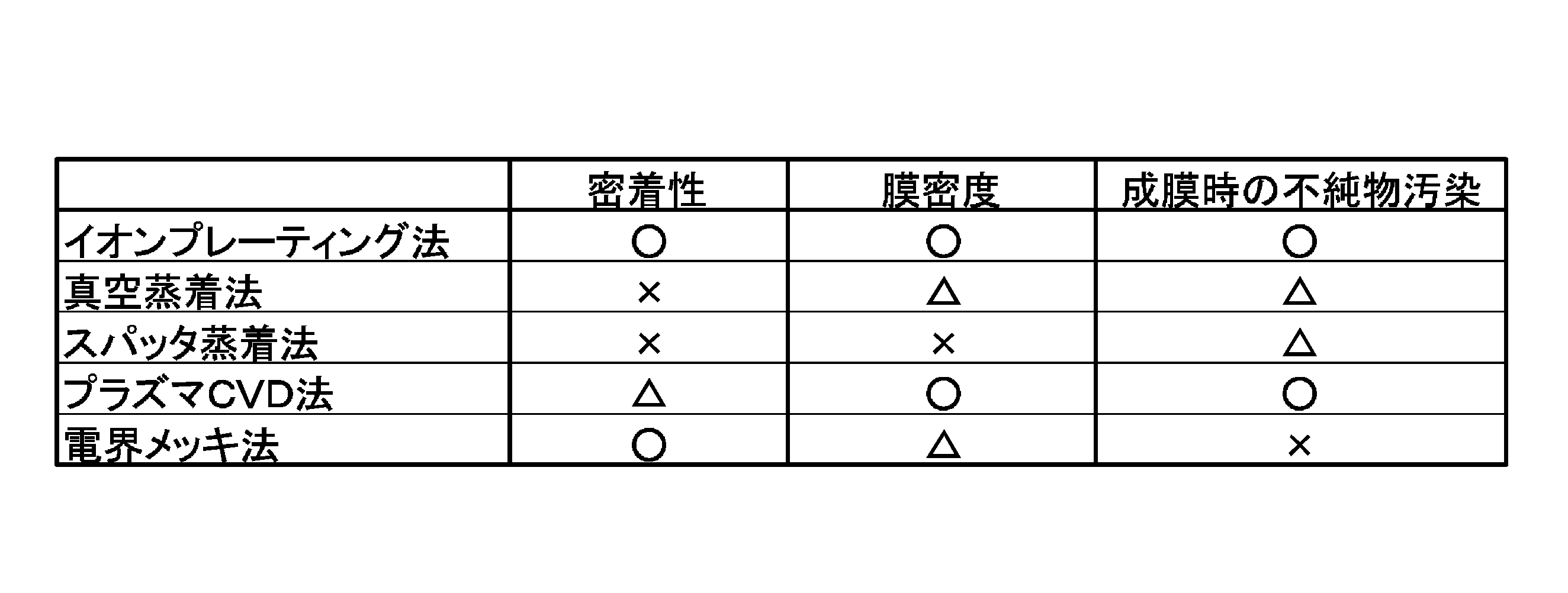
表4に示すように、イオンプレーティング法で白金膜を形成すると、密着性、膜密度、成膜時の不純物汚染の度合いの全てが良好(○)となり、白金膜のコーティング法としてはイオンプレーティング法が特に好ましいことがわかる。
また、プラズマCVD法では、密着性は、イオンプレーティング法を用いたときよりも若干劣る(△)ものの、膜密度及び成膜時の不純物汚染の度合いは良好(○)となっており、プラズマCVD法も白金膜のコーティング法として好ましいことがわかる。
(実施例3)
図3A、図3Bのプラズマコーン18、19(図4A、図4Bのプラズマコーン24、25に白金23を20μm堆積させたもの)と、図4A、図4Bのプラズマコーン24、25(銅母材20の表面にニッケルメッキ21を有し、先端に白金チップ22を有したプラズマコーン)のそれぞれの耐久性(寿命)を調査した。その結果を表5に示す。
図3A、図3Bのプラズマコーン18、19(図4A、図4Bのプラズマコーン24、25に白金23を20μm堆積させたもの)と、図4A、図4Bのプラズマコーン24、25(銅母材20の表面にニッケルメッキ21を有し、先端に白金チップ22を有したプラズマコーン)のそれぞれの耐久性(寿命)を調査した。その結果を表5に示す。

表5に示すように、従来のプラズマコーン(図4A、図4Bのプラズマコーン24、25)の耐久性は3か月程度であったのに対して、白金コーティングを有したプラズマコーン(図3A、図3Bのプラズマコーン18、19)の耐久性は6か月~8か月であり、従来のプラズマコーンの耐久性のおよそ2倍となった。このように、表面に、銅やニッケルに比べて耐食性に優れた白金をコーティングすることで、プラズマコーンの耐久性を向上できることがわかった。
なお、本発明は、上記実施形態に限定されるものではない。上記実施形態は、例示であり、本発明の請求の範囲に記載された技術的思想と実質的に同一な構成を有し、同様な作用効果を奏するものは、いかなるものであったとしても本発明の技術的範囲に包含される。図3A、図3Bでは、図4A、図4Bのプラズマコーン24、25の表面上に白金のコーティング膜23を形成した構成を本発明の実施例として示しているが、図5A、図5Bのプラズマコーン26、27の表面上に白金族金属又は金又はそれらの合金のコーティング膜を形成した構成(つまり、母材全体が白金で形成され、その白金母材の表面上にコーティング膜を形成した構成)を採用してもよい。これによっても、図5A、図5Bのプラズマコーン26、27を用いた場合と同等の感度を達成しつつ、白金母材に起因した不純物バックグランドを低下でき、さらに耐久性も向上できる。
100 誘導結合プラズマ質量分析装置
7 インターフェース部
14 サンプリングコーン(プラズマコーン)
16 スキマーコーン(プラズマコーン)
7 インターフェース部
14 サンプリングコーン(プラズマコーン)
16 スキマーコーン(プラズマコーン)
Claims (4)
- 白金又は白金以外の白金族金属又は金又はそれらの合金のコーティング膜を表面に有することを特徴する誘導結合プラズマ質量分析装置用プラズマコーン。
- 前記コーティング膜は白金で形成されたことを特徴する請求項1に記載の誘導結合プラズマ質量分析装置用プラズマコーン。
- 請求項1又は2に記載の誘導結合プラズマ質量分析装置用プラズマコーンを備えたことを特徴とする誘導結合プラズマ質量分析装置。
- 白金又は白金以外の白金族金属又は金又はそれらの合金のコーティング膜を表面に有するプラズマ質量分析装置用プラズマコーンにおける前記コーティング膜を、イオンプレーティング法又はプラズマCVD法により形成することを特徴とする誘導結合プラズマ質量分析装置用プラズマコーンの製造方法。
Applications Claiming Priority (2)
| Application Number | Priority Date | Filing Date | Title |
|---|---|---|---|
| JP2017-044820 | 2017-03-09 | ||
| JP2017044820A JP2018146536A (ja) | 2017-03-09 | 2017-03-09 | 誘導結合プラズマ質量分析装置用プラズマコーン、誘導結合プラズマ質量分析装置、誘導結合プラズマ質量分析装置用プラズマコーンの製造方法 |
Publications (1)
| Publication Number | Publication Date |
|---|---|
| WO2018163576A1 true WO2018163576A1 (ja) | 2018-09-13 |
Family
ID=63447388
Family Applications (1)
| Application Number | Title | Priority Date | Filing Date |
|---|---|---|---|
| PCT/JP2017/046971 Ceased WO2018163576A1 (ja) | 2017-03-09 | 2017-12-27 | 誘導結合プラズマ質量分析装置用プラズマコーン、誘導結合プラズマ質量分析装置、誘導結合プラズマ質量分析装置用プラズマコーンの製造方法 |
Country Status (3)
| Country | Link |
|---|---|
| JP (1) | JP2018146536A (ja) |
| TW (1) | TW201833363A (ja) |
| WO (1) | WO2018163576A1 (ja) |
Cited By (3)
| Publication number | Priority date | Publication date | Assignee | Title |
|---|---|---|---|---|
| US11667992B2 (en) | 2021-07-19 | 2023-06-06 | Agilent Technologies, Inc. | Tip for interface cones |
| JP2024514918A (ja) * | 2021-04-26 | 2024-04-03 | アジレント・テクノロジーズ・インク | インタフェースコーンのための多層コーティング |
| US12191134B2 (en) | 2019-10-25 | 2025-01-07 | Spacetek Technology Ag | Compact time-of-flight mass analyzer |
Families Citing this family (2)
| Publication number | Priority date | Publication date | Assignee | Title |
|---|---|---|---|---|
| JP6779469B2 (ja) * | 2018-03-27 | 2020-11-04 | 信越半導体株式会社 | 試料分析方法、試料導入装置 |
| GB2585327B (en) | 2018-12-12 | 2023-02-15 | Thermo Fisher Scient Bremen Gmbh | Cooling plate for ICP-MS |
Citations (4)
| Publication number | Priority date | Publication date | Assignee | Title |
|---|---|---|---|---|
| JPH07240169A (ja) * | 1994-02-28 | 1995-09-12 | Jeol Ltd | 誘導結合プラズマ質量分析装置 |
| JPH08236066A (ja) * | 1995-02-27 | 1996-09-13 | Hitachi Ltd | 質量分析装置、スキマ−コ−ン組立体、スキマ−コ−ン及びその製造法 |
| JP2004039313A (ja) * | 2002-06-28 | 2004-02-05 | Toshiba Microelectronics Corp | Icp質量分析装置及びその分析方法 |
| US20120292500A1 (en) * | 2009-05-13 | 2012-11-22 | Micromass Uk Limited | Mass spectrometer sampling cone with coating |
-
2017
- 2017-03-09 JP JP2017044820A patent/JP2018146536A/ja active Pending
- 2017-12-27 WO PCT/JP2017/046971 patent/WO2018163576A1/ja not_active Ceased
-
2018
- 2018-01-16 TW TW107101490A patent/TW201833363A/zh unknown
Patent Citations (4)
| Publication number | Priority date | Publication date | Assignee | Title |
|---|---|---|---|---|
| JPH07240169A (ja) * | 1994-02-28 | 1995-09-12 | Jeol Ltd | 誘導結合プラズマ質量分析装置 |
| JPH08236066A (ja) * | 1995-02-27 | 1996-09-13 | Hitachi Ltd | 質量分析装置、スキマ−コ−ン組立体、スキマ−コ−ン及びその製造法 |
| JP2004039313A (ja) * | 2002-06-28 | 2004-02-05 | Toshiba Microelectronics Corp | Icp質量分析装置及びその分析方法 |
| US20120292500A1 (en) * | 2009-05-13 | 2012-11-22 | Micromass Uk Limited | Mass spectrometer sampling cone with coating |
Cited By (4)
| Publication number | Priority date | Publication date | Assignee | Title |
|---|---|---|---|---|
| US12191134B2 (en) | 2019-10-25 | 2025-01-07 | Spacetek Technology Ag | Compact time-of-flight mass analyzer |
| JP2024514918A (ja) * | 2021-04-26 | 2024-04-03 | アジレント・テクノロジーズ・インク | インタフェースコーンのための多層コーティング |
| US12428719B2 (en) | 2021-04-26 | 2025-09-30 | Agilent Technologies, Inc. | Multilayer coating for interface cones |
| US11667992B2 (en) | 2021-07-19 | 2023-06-06 | Agilent Technologies, Inc. | Tip for interface cones |
Also Published As
| Publication number | Publication date |
|---|---|
| JP2018146536A (ja) | 2018-09-20 |
| TW201833363A (zh) | 2018-09-16 |
Similar Documents
| Publication | Publication Date | Title |
|---|---|---|
| WO2018163576A1 (ja) | 誘導結合プラズマ質量分析装置用プラズマコーン、誘導結合プラズマ質量分析装置、誘導結合プラズマ質量分析装置用プラズマコーンの製造方法 | |
| Koch et al. | Review of the state-of-the-art of laser ablation inductively coupled plasma mass spectrometry | |
| JP3355376B2 (ja) | 質量分析装置、スキマ−コ−ン組立体及びスキマ−コ−ン | |
| Mulders et al. | Fabrication of pure gold nanostructures by electron beam induced deposition with Au (CO) Cl precursor: deposition characteristics and primary beam scattering effects | |
| Milton et al. | Investigations into the suitability of using a secondary cathode to analyse glass using glow discharge mass spectrometry | |
| KR20220028070A (ko) | 내식성 부재 | |
| US6703610B2 (en) | Skimmer for mass spectrometry | |
| US11189474B2 (en) | Sample support, ionization method, and mass spectrometry method | |
| KR102652258B1 (ko) | 금속부품 및 그 제조 방법 및 금속부품을 구비한 공정챔버 | |
| US6765215B2 (en) | Super alloy ionization chamber for reactive samples | |
| Gubal et al. | Combined hollow cathode vs. Grimm cell: semiconductive and nonconductive samples | |
| Priebe et al. | Application of a novel compact Cs evaporator prototype for enhancing negative ion yields during FIB-TOF-SIMS analysis in high vacuum | |
| GB2576970A (en) | Impact ionisation ion source | |
| US6608318B1 (en) | Ionization chamber for reactive samples | |
| Yan et al. | Electroless plating of silver nanoparticles on porous silicon for laser desorption/ionization mass spectrometry | |
| JP5072682B2 (ja) | 質量分析用デバイス、これを用いる質量分析装置および質量分析方法 | |
| JP2018036160A (ja) | 誘導結合プラズマ質量分析方法 | |
| Bustelo et al. | Pulsed radiofrequency glow discharge time-of-flight mass spectrometry for nanostructured materials characterization | |
| Wittmaack | The effect of work function changes on secondary ion energy spectra | |
| WO2014199727A1 (ja) | パラジウムめっき被覆材料およびその製造方法 | |
| JP2016008918A (ja) | 誘導結合プラズマ質量分析方法 | |
| CN107966108A (zh) | 辉光放电光谱法测定铝材表面氧化膜厚度的方法 | |
| JP4060050B2 (ja) | 誘導結合プラズマ質量分析装置用プラズマコーン及び誘導結合プラズマ質量分析装置 | |
| Pisonero et al. | Improving the analytical performance of pulsed-GD-SFMS for multi-elemental depth profile analysis of heat-treated Zn coatings on extruded aluminium | |
| CN107408480B (zh) | 离子注入机 |
Legal Events
| Date | Code | Title | Description |
|---|---|---|---|
| 121 | Ep: the epo has been informed by wipo that ep was designated in this application |
Ref document number: 17899428 Country of ref document: EP Kind code of ref document: A1 |
|
| NENP | Non-entry into the national phase |
Ref country code: DE |
|
| 122 | Ep: pct application non-entry in european phase |
Ref document number: 17899428 Country of ref document: EP Kind code of ref document: A1 |