WO2018159078A1 - 蓄電装置 - Google Patents
蓄電装置 Download PDFInfo
- Publication number
- WO2018159078A1 WO2018159078A1 PCT/JP2017/045845 JP2017045845W WO2018159078A1 WO 2018159078 A1 WO2018159078 A1 WO 2018159078A1 JP 2017045845 W JP2017045845 W JP 2017045845W WO 2018159078 A1 WO2018159078 A1 WO 2018159078A1
- Authority
- WO
- WIPO (PCT)
- Prior art keywords
- negative electrode
- positive electrode
- edge
- electrode
- positive
- Prior art date
- Legal status (The legal status is an assumption and is not a legal conclusion. Google has not performed a legal analysis and makes no representation as to the accuracy of the status listed.)
- Ceased
Links
Images




Classifications
-
- H—ELECTRICITY
- H01—ELECTRIC ELEMENTS
- H01M—PROCESSES OR MEANS, e.g. BATTERIES, FOR THE DIRECT CONVERSION OF CHEMICAL ENERGY INTO ELECTRICAL ENERGY
- H01M50/00—Constructional details or processes of manufacture of the non-active parts of electrochemical cells other than fuel cells, e.g. hybrid cells
- H01M50/50—Current conducting connections for cells or batteries
- H01M50/531—Electrode connections inside a battery casing
-
- H—ELECTRICITY
- H01—ELECTRIC ELEMENTS
- H01G—CAPACITORS; CAPACITORS, RECTIFIERS, DETECTORS, SWITCHING DEVICES, LIGHT-SENSITIVE OR TEMPERATURE-SENSITIVE DEVICES OF THE ELECTROLYTIC TYPE
- H01G11/00—Hybrid capacitors, i.e. capacitors having different positive and negative electrodes; Electric double-layer [EDL] capacitors; Processes for the manufacture thereof or of parts thereof
- H01G11/22—Electrodes
- H01G11/26—Electrodes characterised by their structure, e.g. multi-layered, porosity or surface features
-
- H—ELECTRICITY
- H01—ELECTRIC ELEMENTS
- H01M—PROCESSES OR MEANS, e.g. BATTERIES, FOR THE DIRECT CONVERSION OF CHEMICAL ENERGY INTO ELECTRICAL ENERGY
- H01M10/00—Secondary cells; Manufacture thereof
- H01M10/04—Construction or manufacture in general
-
- H—ELECTRICITY
- H01—ELECTRIC ELEMENTS
- H01M—PROCESSES OR MEANS, e.g. BATTERIES, FOR THE DIRECT CONVERSION OF CHEMICAL ENERGY INTO ELECTRICAL ENERGY
- H01M10/00—Secondary cells; Manufacture thereof
- H01M10/05—Accumulators with non-aqueous electrolyte
- H01M10/058—Construction or manufacture
- H01M10/0585—Construction or manufacture of accumulators having only flat construction elements, i.e. flat positive electrodes, flat negative electrodes and flat separators
-
- H—ELECTRICITY
- H01—ELECTRIC ELEMENTS
- H01M—PROCESSES OR MEANS, e.g. BATTERIES, FOR THE DIRECT CONVERSION OF CHEMICAL ENERGY INTO ELECTRICAL ENERGY
- H01M4/00—Electrodes
- H01M4/02—Electrodes composed of, or comprising, active material
-
- H—ELECTRICITY
- H01—ELECTRIC ELEMENTS
- H01M—PROCESSES OR MEANS, e.g. BATTERIES, FOR THE DIRECT CONVERSION OF CHEMICAL ENERGY INTO ELECTRICAL ENERGY
- H01M4/00—Electrodes
- H01M4/02—Electrodes composed of, or comprising, active material
- H01M4/13—Electrodes for accumulators with non-aqueous electrolyte, e.g. for lithium-accumulators; Processes of manufacture thereof
-
- Y—GENERAL TAGGING OF NEW TECHNOLOGICAL DEVELOPMENTS; GENERAL TAGGING OF CROSS-SECTIONAL TECHNOLOGIES SPANNING OVER SEVERAL SECTIONS OF THE IPC; TECHNICAL SUBJECTS COVERED BY FORMER USPC CROSS-REFERENCE ART COLLECTIONS [XRACs] AND DIGESTS
- Y02—TECHNOLOGIES OR APPLICATIONS FOR MITIGATION OR ADAPTATION AGAINST CLIMATE CHANGE
- Y02E—REDUCTION OF GREENHOUSE GAS [GHG] EMISSIONS, RELATED TO ENERGY GENERATION, TRANSMISSION OR DISTRIBUTION
- Y02E60/00—Enabling technologies; Technologies with a potential or indirect contribution to GHG emissions mitigation
- Y02E60/10—Energy storage using batteries
-
- Y—GENERAL TAGGING OF NEW TECHNOLOGICAL DEVELOPMENTS; GENERAL TAGGING OF CROSS-SECTIONAL TECHNOLOGIES SPANNING OVER SEVERAL SECTIONS OF THE IPC; TECHNICAL SUBJECTS COVERED BY FORMER USPC CROSS-REFERENCE ART COLLECTIONS [XRACs] AND DIGESTS
- Y02—TECHNOLOGIES OR APPLICATIONS FOR MITIGATION OR ADAPTATION AGAINST CLIMATE CHANGE
- Y02P—CLIMATE CHANGE MITIGATION TECHNOLOGIES IN THE PRODUCTION OR PROCESSING OF GOODS
- Y02P70/00—Climate change mitigation technologies in the production process for final industrial or consumer products
- Y02P70/50—Manufacturing or production processes characterised by the final manufactured product
Definitions
- the present invention relates to a power storage device including an electrode assembly.
- lithium ion secondary batteries nickel metal hydride secondary batteries, and the like are known as secondary batteries that are a type of power storage device.
- a lithium ion secondary battery includes an electrode assembly in which a sheet-like positive electrode and a negative electrode are stacked (for example, Patent Document 1).
- a positive electrode sheet 80 as a positive electrode includes a rectangular sheet-like positive metal thin plate 81 and a positive electrode present on both surfaces of the positive metal thin plate 81. A coating region 82. Further, the positive electrode sheet 80 includes a positive electrode uncoated region 83 where the positive electrode thin metal plate 81 is exposed at a location where the positive electrode coated region 82 does not exist in the positive electrode thin metal plate 81. The positive electrode uncoated region 83 exists along one end edge of the positive electrode sheet 80 and includes a positive electrode tab portion 84 as a tab having a shape protruding from a part of one end edge of the positive electrode sheet 80.
- the negative electrode sheet 85 as the negative electrode exists on both surfaces of the rectangular sheet-like negative metal thin plate 86 and the negative metal thin plate 86. And a negative electrode coating region 87 to be provided.
- the negative electrode sheet 85 includes a negative electrode tab portion 88 as a tab having a shape protruding from a part of one end edge.
- the negative electrode sheet 85 has a negative electrode coated region 87 up to the base of the negative electrode tab portion 88, and, like the positive electrode sheet 80, an uncoated region where the negative electrode metal thin plate 86 is exposed over the entire edge. Does not exist.
- a paste-like active material mixture in which active material particles, a conductive agent, and a binder are mixed is applied to the surface of a long metal foil, and the active material mixture After drying, the electrode material is manufactured by pressing to increase the active material density. Thereafter, when the electrode material is cut into the shape of a positive electrode or a negative electrode, a coated region is formed from the layer of the active material mixture, and an uncoated region including a tab portion is formed from the long metal foil.
- the negative electrode coating region 87 is formed up to the root of the negative electrode tab portion 88.
- the protruding one end edge of the tab is formed by cutting the active material mixture layer in the electrode material, and the active material is formed from the cut portion.
- the electrode assembly is used in a state where the edge from which the tab protrudes is at the top. For this reason, if the active material dropped during cutting remains attached to the protruding edge of the tab, the active material falls in the electrode assembly and penetrates between the layers of the electrode assembly, breaks through the separator and causes a short circuit.
- An object of the present invention is to provide a power storage device that can suppress the falling off of an active material from the protruding edge of a tab.
- a power storage device for solving the above problems is a power storage device having an electrode assembly in which a plurality of positive electrodes and a plurality of negative electrodes are alternately stacked in a state of being insulated from each other,
- a positive electrode current collector the positive electrode current collector includes a rectangular positive electrode main body part, and a positive electrode tab protruding from a part of the first positive electrode edge of the positive electrode main body part; and the positive electrode A positive electrode coating portion having a second positive electrode edge portion opposite to the first positive electrode edge portion of the main body portion, and formed by applying a positive electrode active material mixture to a surface of the positive electrode main body portion; A positive electrode active material mixture is not applied along the positive electrode edge portion, and the positive electrode uncoated portion of the positive electrode main body portion is exposed; in the positive electrode, the first positive electrode edge portion and the second positive electrode edge portion; The direction in which the straight line that connects the shortest distances is defined as the height direction, and the positive electrode is not coated in the height direction.
- the height of the positive electrode uncoated portion is designed, and the amount of deviation assumed in the design is assumed as the assumed deviation amount, and the height of the positive electrode uncoated portion is the median value set in the design. And a value set larger than the assumed deviation amount, and the assumed deviation amount satisfies the following expression, 0 ⁇ assumed deviation amount ⁇ 3 mm, and is one end in the height direction of the positive electrode coating portion.
- the negative electrode comprises a negative electrode current collector, the negative electrode current collector is a rectangular negative electrode body, A negative electrode tab having a shape protruding from a part of the first negative electrode edge of the negative electrode main body, and having a second negative electrode edge opposite to the first negative electrode edge of the negative electrode main body, A negative electrode coating portion formed by applying a negative electrode active material mixture to the surface of the negative electrode main body; and the negative electrode comprises the first negative electrode A direction in which a straight line connecting the edge portion and the second negative electrode edge portion with the shortest distance is defined as a height direction, located at one end in the height direction of the negative electrode coating portion, and an edge portion on the first negative electrode edge portion side Is the first negative electrode coating edge, the first negative electrode coating edge is designed, on the first negative electrode edge, or closer to the second negative electrode edge than the first negative electrode edge.
- the gist is that it is located at one end in the height direction from the positive electrode coating edge.
- the first negative electrode coating edge is closer to the second negative electrode edge than the first negative electrode edge, and the negative electrode An exposed negative electrode uncoated portion of the negative electrode current collector is formed along the first negative electrode edge. Further, when the height of the negative electrode coating portion is shifted by the maximum amount of deviation assumed in design, the first negative electrode coating edge portion is located on the first negative electrode edge portion.
- Such a negative electrode is manufactured by cutting an electrode material obtained by applying a negative electrode active material mixture to a long metal foil. During the cutting, the negative electrode tab is formed to form a protruding first negative electrode edge. In this case, the coated part is not cut, and the negative electrode active material does not fall off due to the cutting of the coated part.
- the height of the positive electrode uncoated portion is the sum of the design median value and a value set larger than the assumed deviation amount. Even if the position of the positive electrode uncoated portion is shifted by an assumed shift amount, the positive electrode uncoated portion is secured. For this reason, even if a deviation occurs in the application of the positive electrode active material mixture, it is applied to the positive electrode uncoated portion, avoiding the formation of the positive electrode coated portion on the positive electrode tab, and generating an active material that does not contribute to battery capacity Can be eliminated. Moreover, it can control that a positive electrode uncoated part becomes larger than necessary by setting the assumption deviation
- the first negative electrode coating edge is positioned at one end in the height direction from the positive electrode coating edge, so that the entire surface of the positive electrode coating part can be opposed to the negative electrode coating part.
- the first negative electrode coating edge portion coincides with the first negative electrode edge portion. According to this, the negative electrode coating portion is not formed on the negative electrode tab, and even if the negative electrode tab is folded in a stacked state, the negative electrode coating portion does not become an obstacle to the bending of the negative electrode tab, and is not bent. There is no loss of the negative electrode active material.
- a range larger than the assumed deviation amount in the positive electrode uncoated portion is 1.0 mm or less. According to this, since the height of the positive electrode uncoated portion is set to be larger in the range of 1 mm or less than the assumed deviation amount, the positive electrode uncoated portion even if a deviation occurs by the assumed deviation amount. Can be secured.
- a power storage device for solving the above problems is a power storage device having an electrode assembly in which a plurality of positive electrodes and a plurality of negative electrodes are alternately stacked in a state of being insulated from each other,
- a positive electrode current collector, the positive electrode current collector includes a rectangular positive electrode main body part, and a positive electrode tab protruding from a part of the first positive electrode edge of the positive electrode main body part; and the positive electrode A positive electrode coating portion having a second positive electrode edge portion opposite to the first positive electrode edge portion of the main body portion, and formed by applying a positive electrode active material mixture to a surface of the positive electrode main body portion;
- a positive electrode active material mixture is not applied along the positive electrode edge portion, and the positive electrode uncoated portion of the positive electrode main body portion is exposed; in the positive electrode, the first positive electrode edge portion and the second positive electrode edge portion;
- the direction in which the straight line that connects the shortest distances extends is the height direction, and the positive electrode is not coated
- the negative electrode is provided with a negative electrode current collector, the negative electrode current collector is a rectangular negative electrode main body, and a part of the first negative electrode edge of the negative electrode main body.
- a negative electrode tab having a shape protruding from the second negative electrode edge, and having a second negative electrode edge that is opposite to the first negative electrode edge of the negative electrode body, and a negative electrode active material mixture on the surface of the negative electrode body
- the negative electrode coating portion is formed by coating, and the negative electrode has a height direction in which a straight line connecting the first negative electrode edge portion and the second negative electrode edge portion with the shortest distance is defined as the height direction.
- the edge on the first negative electrode edge side is a first negative electrode coating edge located at one end in the height direction of the work part, the first negative electrode coating edge And, by design, located on the first negative electrode edge, or closer to the second negative electrode edge than the first negative electrode edge, and located closer to one end in the height direction than the positive electrode coating edge.
- the first negative electrode coating edge is closer to the second negative electrode edge than the first negative electrode edge, and the negative electrode An exposed negative electrode uncoated portion of the negative electrode current collector is formed along the first negative electrode edge. Further, when the height of the negative electrode coating portion is shifted by the maximum amount of deviation assumed in design, the first negative electrode coating edge portion is located on the first negative electrode edge portion.
- Such a negative electrode is manufactured by cutting an electrode material obtained by applying a negative electrode active material mixture to a long metal foil. During the cutting, the negative electrode tab is formed to form a protruding first negative electrode edge. In this case, the coated part is not cut, and the negative electrode active material does not fall off due to the cutting of the coated part.
- the height of the positive electrode uncoated portion is 0.5 to 2.0 mm. For this reason, even if the position of a positive electrode uncoated part shifts
- the first negative electrode coating edge is positioned at one end in the height direction from the positive electrode coating edge, so that the entire surface of the positive electrode coating part can be opposed to the negative electrode coating part.
- the height of the positive electrode uncoated portion is 0.8 to 1.2 mm. According to this, the dimension of the positive electrode uncoated part in the height direction is brought close to a tolerance of 1 mm.
- the positive electrode tab is bent from the base end side near the first positive electrode edge, and a direction from the bent portion toward the tip extends in the stacking direction of the positive electrode and the negative electrode.
- the positive electrode coated portion is not formed on the positive electrode tab. For this reason, compared with the case where the positive electrode coating part is formed in the positive electrode tab, when bending a positive electrode tab, the stress which generate
- the active material can be prevented from falling off from the protruding edge of the tab.
- the disassembled perspective view which shows the secondary battery of embodiment.
- the disassembled perspective view which shows the component of an electrode assembly.
- the top view which shows the positive electrode and negative electrode of embodiment.
- the partial cross section side view which shows an electrode assembly.
- the figure which shows manufacture of a negative electrode. (A) is a figure which shows the positive electrode sheet of background art, (b) is a figure which shows the negative electrode sheet of background art.
- the secondary battery 10 includes a metal case 11 constituting an outer shell.
- the case 11 includes a bottomed rectangular parallelepiped case body 12 having an opening 12a, and a lid 13 that closes the opening 12a.
- the case 11 contains an electrode assembly 14 and an electrolytic solution (not shown) as an electrolyte.
- the secondary battery 10 is a lithium ion secondary battery.
- a plurality of positive electrodes 21 and a plurality of negative electrodes 24 are alternately stacked with a resin separator 27 interposed therebetween. It has a laminated structure.
- a direction in which the positive electrode 21, the negative electrode 24, and the separator 27 are stacked is defined as a stacking direction.
- the positive electrode 21, the negative electrode 24, and the separator 27 are rectangular when viewed from the stacking direction.
- the positive electrode 21 includes a positive metal foil (in this embodiment, an aluminum foil) 22 as a positive electrode current collector.
- the positive electrode metal foil 22 is a rectangular positive electrode main body portion 22a and one of the first positive electrode edge portions 22b serving as one of the edges along the pair of long sides of the positive electrode main body portion 22a.
- a positive electrode tab 31 protruding from the portion.
- the positive electrode 21 includes a positive electrode uncoated portion M along the first positive electrode edge portion 22b of the positive electrode main body portion 22a.
- the positive electrode uncoated portion M has a certain width along the direction in which the first positive electrode edge portion 22b extends.
- the positive electrode 21 has the positive electrode coating part 23 which exists in both surfaces of the positive electrode main-body part 22a.
- the positive electrode coating part 23 is formed by applying a positive electrode active material mixture to the positive electrode main body part 22a.
- the positive electrode uncoated portion M exists in a portion where the positive electrode coated portion 23 does not exist in the positive electrode main body portion 22a.
- the positive electrode uncoated portion M is an exposed portion of the positive electrode main body portion 22a without being applied with the positive electrode active material mixture along the first positive electrode edge portion 22b.
- the positive electrode main body 22 a has a second positive electrode edge 22 c at an end along the other long side that is the opposite side of the first positive electrode edge 22 b, and the first positive electrode edge 22 b and the second positive electrode
- a third positive electrode edge 22d is provided at the edge along the pair of short sides connecting the edge 22c.
- the extending direction of the first positive electrode edge portion 22b and the second positive electrode edge portion 22c is defined as the width direction.
- the positive electrode coating part 23 has the 1st positive electrode coating edge part 23a in the edge part nearest to the positive electrode uncoated part M in the height direction. Moreover, the positive electrode coating part 23 has the 2nd positive electrode coating edge part 23b in the opposite side of the 1st positive electrode coating edge part 23a, and the 2nd positive electrode coating edge part 23b is the 2nd positive electrode of the positive electrode main-body part 22a. Along the edge portion 22c, the second positive electrode coating edge portion 23b and the second positive electrode edge portion 22c are flush with each other.
- the positive electrode coating portion 23 has a third positive electrode coating edge portion 23c at a pair of end edges connecting the first positive electrode coating edge portion 23a and the second positive electrode coating edge portion 23b.
- Each third positive electrode coating edge 23c extends along the third positive electrode edge 22d of the positive electrode main body 22a, and the third positive electrode coating edge 23c and the third positive electrode edge 22d are flush with each other.
- the first positive electrode coating edge 23a is located closer to the second positive electrode edge 22c than the first positive electrode edge 22b of the positive electrode body 22a. For this reason, the positive electrode 21 includes a positive electrode uncoated portion M in a portion where the positive electrode main body portion 22a is exposed along the first positive electrode edge portion 22b.
- the dimension from the first positive electrode coating edge portion 23a to the second positive electrode coating edge portion 23b along the height direction is defined as a height H1 of the positive electrode coating portion 23.
- the dimension from the first positive electrode coating edge 23 a to the first positive electrode edge 22 b along the height direction is defined as a height Hm of the positive electrode uncoated part M.
- the negative electrode 24 includes a sheet-like negative metal foil (copper foil in this embodiment) 25 as a negative electrode current collector.
- the negative electrode metal foil 25 is a rectangular negative electrode main body 25a and one of the first negative electrode edge 25b serving as one of the edges along the pair of long sides of the negative electrode main body 25a.
- a negative electrode tab 32 having a shape protruding from the portion.
- the negative electrode 24 includes a negative electrode uncoated portion N along the first negative electrode edge 25b of the negative electrode main body 25a.
- the negative electrode uncoated portion N has a certain width along the direction in which the first negative electrode edge 25b extends.
- the negative electrode 24 has the negative electrode coating part 26 which exists in both surfaces of the negative electrode main-body part 25a.
- the negative electrode coating part 26 is formed by applying a negative electrode active material mixture to the negative electrode main body part 25a.
- the negative electrode uncoated portion N exists in a portion where the negative electrode coated portion 26 does not exist in the negative electrode main body portion 25a.
- the negative electrode uncoated portion N is an exposed portion of the negative electrode main body portion 25a where the negative electrode active material mixture is not applied along the first negative electrode edge portion 25b.
- the negative electrode main body 25a has a second negative electrode edge 25c at the edge along the other long side that is the opposite side of the first negative electrode edge 25b, and connects the first negative electrode edge 25b and the second negative electrode edge 25c.
- a third negative electrode edge portion 25d is provided at the edge along the pair of short sides.
- the direction in which the straight line L2 that connects the first negative electrode edge 25b and the second negative electrode edge 25c with the shortest distance extends is the height direction.
- the extending direction of the first negative electrode edge 25b and the second negative electrode edge 25c is defined as the width direction.
- the negative electrode coating part 26 has the 1st negative electrode coating edge part 26a in the edge part nearest to the negative electrode uncoated part N in the height direction.
- the negative electrode coating portion 26 has a second negative electrode coating edge portion 26b on the opposite side of the first negative electrode coating edge portion 26a, and the second negative electrode coating edge portion 26b is a second negative electrode edge portion of the negative electrode main body portion 25a.
- the second negative electrode coating edge 26b and the second negative electrode edge 25c are flush with each other along the line 25c.
- the negative electrode coating portion 26 has a third negative electrode coating edge portion 26c at a pair of end edges connecting the first negative electrode coating edge portion 26a and the second negative electrode coating edge portion 26b.
- Each third negative electrode coating edge 26c extends along the third negative electrode edge 25d of the negative electrode main body 25a, and the third negative electrode coating edge 26c and the third negative electrode edge 25d are flush with each other.
- the first negative electrode coating edge 26a is located closer to the second negative electrode edge 25c than the first negative electrode edge 25b of the negative electrode body 25a. For this reason, the negative electrode 24 includes a negative electrode uncoated portion N in a portion where the negative electrode main body portion 25a is exposed along the first negative electrode edge portion 25b.
- the dimension from the first negative electrode coating edge portion 26a along the height direction to the second negative electrode coating edge portion 26b is defined as a height H2 of the negative electrode coating portion 26.
- the dimension from the first negative electrode coated edge portion 26a to the first negative electrode edge portion 25b along the height direction is defined as a height Hn of the negative electrode uncoated portion N.
- the negative electrode 24 is manufactured by cutting a long strip-shaped electrode material 33 with a laser along the two-dot chain line in FIG.
- the electrode material 33 is provided on both sides of the long metal foil 34 that forms the negative electrode metal foil 25 of the negative electrode 24 and the negative electrode active material mixture that forms the negative electrode coating portion 26.
- the negative electrode active material mixture is a paste in which a negative electrode active material, a conductive agent, and a binder are mixed.
- the negative electrode active material mixture is applied at regular intervals in the longitudinal direction of the long metal foil 34.
- the dimension of the electrode material 33 in the short direction is longer than the dimensions of the first negative electrode edge 25b and the second negative electrode edge 25c, and the coating part 35 is formed over the entire short direction of the electrode material 33. ing. Then, the electrode material 33 is cut into the outer shape of the negative electrode 24 by the laser irradiated from the laser processing apparatus.
- the positive electrode 21 of the present embodiment is manufactured by punching a long strip electrode material with a punching die.
- the positive electrode active material mixture used for manufacturing the positive electrode 21 is a paste in which a positive electrode active material, a conductive agent, and a binder are mixed.
- the positive electrode 21 and the negative electrode 24 having the above-described configuration are stacked with a separator 27 sandwiched between the positive electrode 21 and the negative electrode 24 to form the electrode assembly 14. ing.
- Each positive electrode 21 is laminated so that the respective positive electrode tabs 31 are arranged in a row along the lamination direction.
- Each of the stacked positive electrode tabs 31 is bent from the base end side near the first positive electrode edge 22b, and the direction from the bent portion toward the tip is the stacking direction.
- each negative electrode 24 is laminated so that the respective negative electrode tabs 32 are arranged in a row along the lamination direction so as not to overlap the positive electrode tab 31.
- the negative electrode tabs 32 in the stacked state are bent from the base end side near the first negative electrode edge portion 25b, and the direction from the bent portion toward the tip is the stacking direction.
- the positive electrode tab 31 and the negative electrode tab 32 protrude from the same end surface of the electrode assembly 14 in the same direction.
- the positive electrode tab 31 of each positive electrode 21 is bent in a stacked state and is electrically connected to the positive electrode terminal 15.
- the negative electrode tab 32 of each negative electrode 24 is also folded in a stacked state and is electrically connected to the negative electrode terminal 16.
- the electrode assembly 14 needs to be laminated so that the negative electrode coating part 26 faces the entire surface of the positive electrode coating part 23 through the separator 27. For this reason, the height H ⁇ b> 2 in the negative electrode coating part 26 is set longer than the height H ⁇ b> 1 of the positive electrode coating part 23.
- the positive electrode 21 and the negative electrode 24 are laminated such that the first positive electrode coating edge portion 23a is located on the lower side in the height direction than the first negative electrode coating edge portion 26a. That is, the first negative electrode coating edge portion 26a is located on one end side in the height direction from the first positive electrode coating edge portion 23a.
- the positive electrode 21 and the negative electrode 24 are laminated so that the first positive electrode edge 22b is positioned below the first negative electrode edge 25b.
- the positive electrode 21 and the negative electrode 24 are stacked such that the second positive electrode coating edge 23 b is positioned higher in the height direction than the second negative electrode coating edge 26 b.
- the positive electrode 21 and the negative electrode 24 are stacked such that the second positive electrode edge 22c is positioned above the second negative electrode edge 25c.
- the positive electrode uncoated part M is manufactured aiming at the value (henceforth a median value) set at the time of design about height Hm.
- the actual size of the height Hm may deviate from the median value due to various factors.
- the factors are mostly based on the manufacture of the positive electrode 21, for example, due to a shift in the application of the active material mixture, the active material mixture being separately applied to the long metal foil 34 one side at a time. There is a gap.
- there are two deviations namely, a deviation at the time of punching due to a deviation in the punching location, and a deviation due to the active material mixture being separately applied to the long metal foil 34 one by one.
- the maximum tolerance is set to 1.0 mm.
- the height Hm of the positive electrode uncoated portion M is set to a median value of an assumed deviation amount (hereinafter, an assumed deviation amount x) so that the positive electrode uncoated portion M is formed. It is set by adding a larger value. Therefore, a design shift amount is assumed in advance for the height Hm of the positive electrode uncoated portion M.
- an assumed deviation amount x an assumed deviation amount
- the assumed deviation amount x includes a case where the value of the height Hm is larger than the median value and a case where the value of the height Hm is smaller than the median value. Will be described as a case where the value of the height Hm is greater than the median value.
- the larger the set assumed deviation amount x is the more the first positive electrode edge portion 22b and the first positive electrode coating edge portion 23a are separated, and the value of the height Hm of the positive electrode uncoated portion M is increased. M gets higher.
- the smaller the set assumed deviation amount x the closer the first positive electrode edge 22b and the first positive electrode coating edge 23a are, and the value of the height Hm of the positive electrode uncoated area M becomes smaller.
- the construction part M becomes lower.
- the assumed deviation amount x is expressed by the following equation: 0 ⁇ assumed deviation x ⁇ 3 mm It was.
- the positive electrode uncoated portion M is restricted from becoming larger than necessary.
- the height Hm of the positive electrode uncoated portion M is set to be larger than the assumed deviation amount x in a range of 1 mm or less.
- the height Hm of the positive electrode uncoated portion M set in this way is preferably set to 0.5 to 2.0 mm, and preferably set to 0.8 to 1.2 mm. More preferred. With this configuration, the height Hm of the positive electrode uncoated portion M can be brought close to a tolerance of 1.0 mm. In the present embodiment, in the positive electrode 21, the Hm of the positive electrode uncoated portion M is set to 1.2 mm.
- the negative electrode coating part 26 is manufactured with the aim of the height H2 set at the time of design (hereinafter referred to as the median).
- the actual size of the height H2 of the negative electrode coating portion 26 may deviate from the median value due to various factors. Many of the factors are based on the production of the negative electrode 24.
- the active material mixture is shifted during application, and the active material mixture is applied separately to the long metal foil 34 one side at a time. There is a gap. Even if these deviations occur, the height H2 of the negative electrode coating portion 26 is described as an assumed deviation amount (hereinafter referred to as an assumed deviation amount y) so that the negative electrode coating portion 26 is not formed on the negative electrode tab 32. ) Is set larger than. Therefore, a design shift amount is assumed in advance for the height H2 of the negative electrode coating portion 26.
- the assumed deviation amount y includes a case where the value of the height H2 of the negative electrode coating portion 26 is larger than the median value and a case where the value of the height H2 is smaller than the median value.
- the assumed deviation amount y will be described as a case where the value of the height H2 is larger than the median value.
- the first negative electrode coating edge portion 26a and the first negative electrode edge portion 25b are closer, the value of the height H2 of the negative electrode coating portion 26 is larger, and the negative electrode uncoated portion N is lower.
- the first negative electrode coated edge portion 26a coincides with the first negative electrode edge portion 25b, and the negative electrode uncoated portion N is not formed, but the negative electrode tab 32 has a negative electrode coated portion. 26 is not formed.
- the assumed deviation amount y is smaller, the first negative electrode coated edge portion 26a and the first negative electrode edge portion 25b are separated from each other, and the value of the height H2 of the negative electrode coated portion 26 is decreased, and the negative electrode uncoated portion. N increases.
- the negative electrode 24 when the negative electrode 24 is manufactured, when the negative electrode active material mixture is applied according to the design median value and the electrode material 33 is cut according to the median value, the first negative electrode edge 25b of the negative electrode 24 is obtained. 4 is cut by cutting the long metal foil 34 in a state parallel to the first negative electrode coating edge portion 26a of the negative electrode coating portion 26, as indicated by a two-dot chain line in FIG. Therefore, the manufactured negative electrode 24 includes the negative electrode uncoated portion N, and the edge itself of the coated portion 35 along the negative electrode uncoated portion N becomes the first negative electrode coated edge portion 26a.
- the second negative electrode coating edge 26b and the third negative electrode coating edge 26c of the negative electrode 24 are formed by cutting with a laser.
- the negative electrode active material mixture may be applied according to the design median value, but may be cut from the design median value.
- the assumed deviation amount y is the maximum, that is, when the first negative electrode coating edge portion 26a is located on the first negative electrode edge portion 25b, the cutting of the portion that becomes the first negative electrode edge portion 25b of the negative electrode 24 is As shown by a two-dot chain line in FIG. 6, the long metal foil 34 is cut along the coating portion 35.
- the manufactured negative electrode 24 does not include the negative electrode uncoated portion N, but the edge of the coated portion 35 itself becomes the first negative electrode coated edge portion 26a.
- the effect of the secondary battery 10 will be described.
- the first negative electrode coating edge portion 26a is more second negative edge than the first negative electrode edge portion 25b. Near the portion 25c, the negative electrode uncoated portion N is formed.
- the 1st negative electrode coating edge part 26a is located on the 1st negative electrode edge part 25b on design. For this reason, when the negative electrode 24 is manufactured by cutting the electrode material 33, the coating part 35 is not cut for the formation of the protruding first negative electrode edge 25b of the negative electrode tab 32.
- the cutting for forming the first negative electrode edge portion 25b is performed when the negative electrode coating portion 26 is manufactured with a median value and when the maximum estimated deviation amount y is shifted. In any case, the long metal foil 34 is cut. For this reason, compared with the case where the cutting of the electrode material 33 for forming the first negative electrode edge 25b is the cutting at the coating part 35, the negative electrode 24 can be manufactured easily and quickly.
- the first negative electrode coating edge 26a is on the first negative electrode edge 25b. Even in this case, the negative electrode coating portion 26 is not formed on the negative electrode tab 32, and the negative electrode coating portion 26 is not bent on the negative electrode tab 32 even if the negative electrode tab 32 is folded in a stacked state. There is no hindrance, and there is no loss of the negative electrode active material due to bending.
- the negative electrode 24 has the negative electrode uncoated portion N except that the assumed deviation amount y is maximized.
- the electrode assembly 14 may be pressed toward the case body 12 by the lid body 13.
- the negative electrode uncoated portion N of the negative electrode 24 is pressed by the lid body 13, so that the lid body 13 can be prevented from coming into contact with the negative electrode coated portion 26, and the negative electrode active material is removed from the negative electrode coated portion 26. Can be suppressed.
- the negative electrode uncoated portion N can be bent to prevent the bottom surface of the electrode assembly 14 from colliding with the inner bottom surface of the case body 12.
- the height Hm of the positive electrode uncoated portion M was set to be larger than the sum of the median and the assumed deviation amount x. For this reason, for example, even if the position of the first positive electrode edge portion 22b is shifted to the second positive electrode edge portion 22c side by the assumed deviation amount x, as shown in FIG. 3, the first positive electrode edge portion 22b is shown by the two-dot chain line T1.
- the positive electrode uncoated portion M is secured at the location shown in FIG. Further, even if the position of the first positive electrode coating edge portion 23a is shifted to the first positive electrode edge portion 22b side by the assumed deviation amount x, the first positive electrode coating edge portion 23a is positioned at a position indicated by a two-dot chain line T2.
- the positive electrode uncoated portion M is secured.
- the assumed deviation amount x of the positive electrode uncoated portion M was set to 0 ⁇ assumed deviation amount x ⁇ 3 mm.
- the assumed deviation amount x was set to 0 ⁇ assumed deviation amount x ⁇ 3 mm.
- the positive electrode uncoated part M is formed, and even if a deviation occurs in the application of the positive electrode active material mixture, the positive electrode uncoated part M is applied.
- the formation of the positive electrode coating portion 23 on the positive electrode tab 31 can be avoided, and the generation of an active material that does not contribute to the battery capacity can be eliminated.
- it can control that the positive electrode uncoated part M becomes larger than necessary by setting the assumed maximum deviation amount x to 3 mm or less.
- the assumed deviation amount x of the positive electrode uncoated portion M was set to 0 ⁇ assumed deviation amount x ⁇ 3 mm.
- the positive electrode uncoated portion M can be formed. For this reason, when manufacturing the positive electrode 21 by cutting the electrode material 33, the coating part 35 is not cut to form the first positive electrode edge 22b protruding from the positive electrode tab 31, and the coating part There is no loss of the positive electrode active material due to the cutting of 35.
- the positive electrode active material from the first positive electrode edge 22b can be prevented, and the positive electrode active material can be prevented from entering between the layers of the electrode assembly 14.
- the height Hm of the positive electrode uncoated portion M is set to be larger than the assumed deviation amount x in a range of 1 mm or less. For this reason, the positive electrode uncoated portion M can be secured even if a deviation occurs by the assumed deviation amount x.
- the height Hm of the positive electrode uncoated portion M is preferably set to 0.5 to 2.0 mm, more preferably 0.8 to 1.2 mm. With this configuration, the height Hm of the positive electrode uncoated portion M can be brought close to a tolerance of 1.0 mm.
- the positive electrode tab 31 is bent from the proximal end side near the first positive electrode edge 22b. Then, by forming the positive electrode uncoated portion M on the positive electrode 21, the positive electrode coated portion 23 is not formed on the positive electrode tab 31. For this reason, compared with the case where the positive electrode coating part 23 is formed in the positive electrode tab 31, when the positive electrode tab 31 is bent, the stress which generate
- the negative electrode tab 32 is bent from the proximal end side near the first negative electrode edge 25b. Then, by forming the negative electrode uncoated portion N on the negative electrode 24, the negative electrode coated portion 26 is not formed on the negative electrode tab 32. For this reason, compared with the case where the negative electrode coating part 26 is formed in the negative electrode tab 32, when bending the negative electrode tab 32, the stress which generate
- the cutting of the electrode material 33 for manufacturing the negative electrode 24 may be performed by punching instead of the laser.
- the secondary battery 10 is a lithium ion secondary battery, but is not limited thereto, and may be another secondary battery. In short, any material may be used as long as ions move between the positive electrode active material and the negative electrode active material and transfer charge.
- the positive electrode current collector is embodied as the positive electrode metal foil 22 and the negative electrode current collector is embodied as the negative electrode metal foil 25.
- the current collector may be a sheet body other than the metal foil as long as the coating portion can be held.
- . -It may be embodied in a power storage device such as an electric double layer capacitor.
- the positive electrode current collector and the negative electrode current collector are metal foils.
- the positive electrode tab and the negative electrode tab exist on the end face of the electrode assembly.
- M positive electrode uncoated part, 10 ... secondary battery as power storage device, 14 ... electrode assembly, 21 ... positive electrode, 22 ... positive electrode metal foil as positive electrode current collector, 22a ... positive electrode body part, 22b ... first DESCRIPTION OF SYMBOLS 1 Positive electrode edge, 22c ... 2nd positive electrode edge, 23 ... Positive electrode coating part, 24 ... Negative electrode, 25 ... Negative electrode metal foil as a negative electrode collector, 25a ... Negative electrode main-body part, 25b ... 1st negative electrode edge 25c, second negative electrode edge, 26, negative electrode coating portion, 26a, first negative electrode coating edge, 31 ... positive electrode tab, 32 ... negative electrode tab.
Landscapes
- Chemical & Material Sciences (AREA)
- Chemical Kinetics & Catalysis (AREA)
- Electrochemistry (AREA)
- General Chemical & Material Sciences (AREA)
- Engineering & Computer Science (AREA)
- Power Engineering (AREA)
- Manufacturing & Machinery (AREA)
- Microelectronics & Electronic Packaging (AREA)
- Materials Engineering (AREA)
- Battery Electrode And Active Subsutance (AREA)
Abstract
二次電池の正極未塗工部の高さにおいて、設計上、想定されるずれ量を想定ずれ量とすると、正極未塗工部の高さは、設計上設定された中央値と、想定ずれ量よりも大きく設定された値との和であり、想定ずれ量は、以下の式、0<想定ずれ量≦3mm、が成立している。また、負極電極の第1負極塗工縁部は、設計上、第1負極縁部よりも第2負極縁部寄りにあり、かつ第1正極塗工縁部より高さ方向一端側にある。
Description
本発明は、電極組立体を備える蓄電装置に関する。
従来から、蓄電装置の一種である二次電池としては、リチウムイオン二次電池や、ニッケル水素二次電池などが知られている。例えば、リチウムイオン二次電池では、シート状の正極電極及び負極電極を積層した電極組立体を備える(例えば、特許文献1)。
特許文献1に開示の蓄電装置において、図7(a)に示すように、正極電極としての正電極シート80は、矩形シート状の正極金属薄板81と、正極金属薄板81の両面に存在する正極塗工領域82とを備える。また、正電極シート80は、正極金属薄板81のうち正極塗工領域82の存在しない箇所に、正極金属薄板81の露出した正極未塗工領域83を備える。正極未塗工領域83は、正電極シート80の一端縁に沿って存在するとともに、正電極シート80の一端縁の一部から突出した形状のタブとしての正電極タブ部84を含む。
また、特許文献1に開示の蓄電装置において、図7(b)に示すように、負極電極としての負電極シート85は、矩形シート状の負極金属薄板86と、負極金属薄板86の両面に存在する負極塗工領域87とを備える。負電極シート85は、一端縁の一部から突出した形状のタブとしての負電極タブ部88を備える。なお、負電極シート85は、負電極タブ部88の根本まで負極塗工領域87が存在し、正電極シート80のように、一端縁全体に亘って負極金属薄板86の露出した未塗工領域は存在しない。
このような正極電極及び負極電極の製造方法の一例としては、活物質粒子、導電剤、及びバインダを混合したペースト状の活物質合剤を長尺金属箔の表面に塗布し、活物質合剤を乾燥させた後、活物質密度を高めるためにプレスし、電極材料を製造する。その後、電極材料を正極電極又は負極電極の形状に切断すると、活物質合剤の層から塗工領域が形成され、長尺金属箔からタブ部を含む未塗工領域が形成される。
ところで、特許文献1に開示の負電極シート85においては、負電極タブ部88の根本にまで負極塗工領域87が形成されている。このため、特許文献1に開示のような負極電極を電極材料から製造する際、タブの突出した一端縁は電極材料における活物質合剤の層を切断して形成され、切断箇所から活物質が脱落する虞がある。電極組立体は、タブが突出する端縁が上部となる状態で使用される場合がほとんどである。このため、タブの突出した端縁に、切断時に脱落した活物質が付着したままであると、電極組立体において活物質が落下して電極組立体の層間に侵入し、セパレータを突き破って短絡の原因となる虞がある。なお、負極電極において、タブの突出した端縁以外の端縁に活物質が付着していても、活物質が落下したときは電極組立体の外での落下になり、電極組立体の層間から内部へ侵入しにくい。このため、負極電極の製造時に発生した活物質に起因した問題は、タブが突出する端縁に特化した問題である。
本発明の目的は、タブの突出した端縁からの活物質の脱落を抑制できる蓄電装置を提供することにある。
上記問題点を解決するための蓄電装置は、複数の正極電極と複数の負極電極とが互いに絶縁された状態で交互に積層された電極組立体を有する蓄電装置であって、前記正極電極は、正極集電体を備えるとともに、該正極集電体は矩形状の正極本体部と、該正極本体部の第1正極縁部の一部から突出した形状の正極タブと、を備え、かつ前記正極本体部の前記第1正極縁部の対辺となる第2正極縁部を有し、前記正極本体部の表面に正極活物質合剤を塗布して形成された正極塗工部と、前記第1正極縁部に沿って正極活物質合剤が塗布されず前記正極本体部の露出した正極未塗工部とを備え、前記正極電極において、前記第1正極縁部と前記第2正極縁部とを最短距離で結ぶ直線の延びる方向を高さ方向とし、該高さ方向への前記正極未塗工部の寸法を高さとし、前記正極未塗工部の高さにおいて、設計上、想定されるずれ量を想定ずれ量とすると、前記正極未塗工部の高さは、設計上設定された中央値と、前記想定ずれ量よりも大きく設定された値との和であり、前記想定ずれ量は、以下の式、0<想定ずれ量≦3mmが成立し、前記正極塗工部の高さ方向一端に位置し、かつ前記第1正極縁部側の縁部を正極塗工縁部とし、前記負極電極は、負極集電体を備えるとともに、該負極集電体は矩形状の負極本体部と、該負極本体部の第1負極縁部の一部から突出した形状の負極タブと、を備え、かつ前記負極本体部の前記第1負極縁部の対辺となる第2負極縁部を有し、前記負極本体部の表面に負極活物質合剤を塗布して形成された負極塗工部を備え、前記負極電極は、前記第1負極縁部と前記第2負極縁部とを最短距離で結ぶ直線の延びる方向を高さ方向とし、前記負極塗工部の高さ方向一端に位置し、かつ前記第1負極縁部側の縁部を第1負極塗工縁部とした場合、前記第1負極塗工縁部は、設計上、前記第1負極縁部上、又は前記第1負極縁部よりも前記第2負極縁部寄りにあり、かつ前記正極塗工縁部より前記高さ方向一端側に位置することを要旨とする。
これによれば、負極塗工部の高さが設計上の中央値で製造された場合、第1負極塗工縁部は第1負極縁部よりも第2負極縁部寄りにあり、負極電極の第1負極縁部に沿って負極集電体の露出した負極未塗工部が形成される。また、負極塗工部の高さが、設計上、想定される最大ずれ量だけずれた場合、第1負極塗工縁部は第1負極縁部上に位置する。このような負極電極は、長尺金属箔に負極活物質合剤を塗布した電極材料を切断して製造されるが、この切断の際、負極タブの突出した第1負極縁部の形成のために塗工部が切断されることはなく、塗工部の切断に伴う負極活物質の脱落がない。
また、正極電極においては、正極未塗工部の高さを、設計上の中央値と、想定ずれ量より大きく設定された値の和としている。想定ずれ量だけ正極未塗工部の位置がずれたとしても、正極未塗工部は確保される。このため、正極活物質合剤の塗布にずれが生じても正極未塗工部に塗布され、正極タブに正極塗工部が形成されることを回避し、電池容量に寄与しない活物質が発生することを無くすことができる。また、想定ずれ量を3mm以下に設定することで、正極未塗工部が必要以上に大きくなることを規制できる。また、電極組立体において、第1負極塗工縁部が正極塗工縁部より高さ方向一端側に位置することにより、正極塗工部の全面を負極塗工部に対向させることができる。
また、蓄電装置について、前記第1負極塗工縁部は、前記第1負極縁部と一致している。
これによれば、負極塗工部が負極タブに形成されることがなく、負極タブが積層された状態で折り曲げられても、負極塗工部が負極タブの折り曲げの障害にならず、折り曲げに伴う負極活物質の脱落もない。
これによれば、負極塗工部が負極タブに形成されることがなく、負極タブが積層された状態で折り曲げられても、負極塗工部が負極タブの折り曲げの障害にならず、折り曲げに伴う負極活物質の脱落もない。
また、蓄電装置について、前記正極未塗工部において、前記想定ずれ量よりも大きくする範囲は1.0mm以下である。これによれば、正極未塗工部の高さは、想定ずれ量よりも1mm以下の範囲で大きくなるように設定されるため、想定ずれ量だけずれが生じたとしても、正極未塗工部を確保できる。
上記問題点を解決するための蓄電装置は、複数の正極電極と複数の負極電極とが互いに絶縁された状態で交互に積層された電極組立体を有する蓄電装置であって、前記正極電極は、正極集電体を備えるとともに、該正極集電体は矩形状の正極本体部と、該正極本体部の第1正極縁部の一部から突出した形状の正極タブと、を備え、かつ前記正極本体部の前記第1正極縁部の対辺となる第2正極縁部を有し、前記正極本体部の表面に正極活物質合剤を塗布して形成された正極塗工部と、前記第1正極縁部に沿って正極活物質合剤が塗布されず前記正極本体部の露出した正極未塗工部とを備え、前記正極電極において、前記第1正極縁部と前記第2正極縁部とを最短距離で結ぶ直線の延びる方向を高さ方向とし、該高さ方向への前記正極未塗工部の寸法を高さとし、前記正極未塗工部の高さは、0.5~2.0mmであり、前記正極塗工部の高さ方向一端に位置し、かつ前記第1正極縁部側の縁部を正極塗工縁部とし、前記負極電極は、負極集電体を備えるとともに、該負極集電体は矩形状の負極本体部と、該負極本体部の第1負極縁部の一部から突出した形状の負極タブと、を備え、かつ前記負極本体部の前記第1負極縁部の対辺となる第2負極縁部を有し、前記負極本体部の表面に負極活物質合剤を塗布して形成された負極塗工部を備え、前記負極電極は、前記第1負極縁部と前記第2負極縁部とを最短距離で結ぶ直線の延びる方向を高さ方向とし、前記負極塗工部の高さ方向一端に位置し、かつ前記第1負極縁部側の縁部を第1負極塗工縁部とした場合、前記第1負極塗工縁部は、設計上、前記第1負極縁部上、又は前記第1負極縁部よりも前記第2負極縁部寄りにあり、かつ前記正極塗工縁部より前記高さ方向一端側に位置することを要旨とする。
これによれば、負極塗工部の高さが設計上の中央値で製造された場合、第1負極塗工縁部は第1負極縁部よりも第2負極縁部寄りにあり、負極電極の第1負極縁部に沿って負極集電体の露出した負極未塗工部が形成される。また、負極塗工部の高さが、設計上、想定される最大ずれ量だけずれた場合、第1負極塗工縁部は第1負極縁部上に位置する。このような負極電極は、長尺金属箔に負極活物質合剤を塗布した電極材料を切断して製造されるが、この切断の際、負極タブの突出した第1負極縁部の形成のために塗工部が切断されることはなく、塗工部の切断に伴う負極活物質の脱落がない。
また、正極電極においては、正極未塗工部の高さを0.5~2.0mmとしている。このため、正極電極の製造時、正極未塗工部の位置がずれたとしても、正極未塗工部は確保される。このため、正極活物質合剤の塗布にずれが生じても正極未塗工部に塗布され、正極タブに正極塗工部が形成されることを回避し、電池容量に寄与しない活物質が発生することを無くすことができる。また、電極組立体において、第1負極塗工縁部が正極塗工縁部より高さ方向一端側に位置することにより、正極塗工部の全面を負極塗工部に対向させることができる。
また、蓄電装置について、前記正極未塗工部の高さは、0.8~1.2mmである。これによれば、高さ方向への正極未塗工部の寸法を公差1mmに近付けることになる。
また、蓄電装置について、前記正極タブは、前記第1正極縁部寄りの基端側から折り曲げられるとともに、折り曲げ部から先端に向かう方向が前記正極電極と前記負極電極の積層方向に延びている。
また、蓄電装置について、前記正極タブは、前記第1正極縁部寄りの基端側から折り曲げられるとともに、折り曲げ部から先端に向かう方向が前記正極電極と前記負極電極の積層方向に延びている。
これによれば、正極電極に正極未塗工部を形成することで、正極タブに正極塗工部が形成されない。このため、正極タブに正極塗工部が形成されている場合と比べると、正極タブを折り曲げときに、折り曲げ部に発生する応力を抑え、正極タブに亀裂等が入ることを抑制しやすくなる。
本発明によれば、タブの突出した端縁からの活物質の脱落を抑制できる。
以下、蓄電装置を二次電池に具体化した一実施形態を図1~図6にしたがって説明する。
図1に示すように、二次電池10は、外郭を構成する金属製のケース11を備えている。ケース11は、開口部12aを備える有底直方体状のケース本体12と、開口部12aを塞ぐ蓋体13とを備えている。ケース11には、電極組立体14及び電解質としての電解液(図示略)が収容されている。二次電池10はリチウムイオン二次電池である。
図1に示すように、二次電池10は、外郭を構成する金属製のケース11を備えている。ケース11は、開口部12aを備える有底直方体状のケース本体12と、開口部12aを塞ぐ蓋体13とを備えている。ケース11には、電極組立体14及び電解質としての電解液(図示略)が収容されている。二次電池10はリチウムイオン二次電池である。
図1又は図2に示すように、電極組立体14は、複数の正極電極21と、複数の負極電極24とが、両者の間に樹脂製のセパレータ27が介在する状態で交互に積み重ねられた積層構造を有する。正極電極21、負極電極24及びセパレータ27が積み重なる方向を積層方向とする。正極電極21、負極電極24及びセパレータ27は、積層方向から見て矩形状である。
正極電極21は、正極集電体としての正極金属箔(本実施形態ではアルミニウム箔)22を備える。積層方向から見て、正極金属箔22は矩形状の正極本体部22aと、正極本体部22aの一対の長辺に沿う端縁のうちの一方の端縁となる第1正極縁部22bの一部から突出した形状の正極タブ31と、を備える。
正極電極21は、正極本体部22aの第1正極縁部22bに沿って正極未塗工部Mを備える。正極未塗工部Mは、第1正極縁部22bの延びる方向に沿って一定幅を有する。正極電極21は、正極本体部22aの両面に存在する正極塗工部23を有する。正極塗工部23は、正極活物質合剤を正極本体部22aに塗布して形成されている。正極未塗工部Mは、正極本体部22aにおいて、正極塗工部23の存在しない部分に存在する。正極未塗工部Mは、第1正極縁部22bに沿って正極活物質合剤が塗布されず正極本体部22aの露出した部分である。
正極電極21において、正極本体部22aは、第1正極縁部22bの対辺となる他方の長辺に沿う端縁に第2正極縁部22cを有し、第1正極縁部22bと第2正極縁部22cを繋ぐ一対の短辺に沿う端縁に第3正極縁部22dを有する。
図3に示すように、積層方向から正極電極21を見て、正極電極21の面方向に沿って第1正極縁部22bと第2正極縁部22cとを最短距離で繋ぐ直線L1の延びる方向を高さ方向とする。また、第1正極縁部22b及び第2正極縁部22cの延びる方向を幅方向とする。
正極塗工部23は、高さ方向において最も正極未塗工部Mに近い縁部に第1正極塗工縁部23aを有する。また、正極塗工部23は、第1正極塗工縁部23aの対辺に第2正極塗工縁部23bを有し、第2正極塗工縁部23bは、正極本体部22aの第2正極縁部22cに沿い、第2正極塗工縁部23bと第2正極縁部22cは面一である。
正極塗工部23は、第1正極塗工縁部23aと第2正極塗工縁部23bを繋ぐ一対の端縁に第3正極塗工縁部23cを有する。各第3正極塗工縁部23cは正極本体部22aの第3正極縁部22dに沿い、第3正極塗工縁部23cと第3正極縁部22dは面一である。
第1正極塗工縁部23aは、正極本体部22aの第1正極縁部22bよりも第2正極縁部22c寄りに位置する。このため、正極電極21は、第1正極縁部22bに沿って正極本体部22aが露出した部分に正極未塗工部Mを備える。
正極電極21において、高さ方向に沿う第1正極塗工縁部23aから第2正極塗工縁部23bまでの寸法を正極塗工部23の高さH1とする。また、正極電極21において、高さ方向に沿う第1正極塗工縁部23aから第1正極縁部22bまでの寸法を正極未塗工部Mの高さHmとする。
次に、負極電極24について説明する。
図2に示すように、負極電極24は、負極集電体としてのシート状の負極金属箔(本実施形態では銅箔)25を備える。積層方向から見て、負極金属箔25は矩形状の負極本体部25aと、負極本体部25aの一対の長辺に沿う端縁のうちの一方の端縁となる第1負極縁部25bの一部から突出した形状の負極タブ32と、を備える。
図2に示すように、負極電極24は、負極集電体としてのシート状の負極金属箔(本実施形態では銅箔)25を備える。積層方向から見て、負極金属箔25は矩形状の負極本体部25aと、負極本体部25aの一対の長辺に沿う端縁のうちの一方の端縁となる第1負極縁部25bの一部から突出した形状の負極タブ32と、を備える。
負極電極24は、負極本体部25aの第1負極縁部25bに沿って負極未塗工部Nを備える。負極未塗工部Nは、第1負極縁部25bの延びる方向に沿って一定幅を有する。負極電極24は、負極本体部25aの両面に存在する負極塗工部26を有する。負極塗工部26は、負極本体部25aに負極活物質合剤を塗布して形成されている。負極未塗工部Nは、負極本体部25aにおいて、負極塗工部26の存在しない部分に存在する。負極未塗工部Nは、第1負極縁部25bに沿って負極活物質合剤が塗布されず負極本体部25aの露出した部分である。
負極本体部25aは、第1負極縁部25bの対辺となる他方の長辺に沿う端縁に第2負極縁部25cを有し、第1負極縁部25bと第2負極縁部25cを繋ぐ一対の短辺に沿う端縁に第3負極縁部25dを有する。
図3に示すように、積層方向から負極電極24を見て、第1負極縁部25bと第2負極縁部25cとを最短距離で繋ぐ直線L2の延びる方向を高さ方向とする。また、第1負極縁部25b及び第2負極縁部25cの延びる方向を幅方向とする。
負極塗工部26は、高さ方向において最も負極未塗工部Nに近い縁部に第1負極塗工縁部26aを有する。負極塗工部26は、第1負極塗工縁部26aの対辺に第2負極塗工縁部26bを有し、第2負極塗工縁部26bは、負極本体部25aの第2負極縁部25cに沿い、第2負極塗工縁部26bと第2負極縁部25cは面一である。
負極塗工部26は、第1負極塗工縁部26aと第2負極塗工縁部26bを繋ぐ一対の端縁に第3負極塗工縁部26cを有する。各第3負極塗工縁部26cは負極本体部25aの第3負極縁部25dに沿い、第3負極塗工縁部26cと第3負極縁部25dは面一である。
第1負極塗工縁部26aは、負極本体部25aの第1負極縁部25bよりも第2負極縁部25c寄りに位置する。このため、負極電極24は、第1負極縁部25bに沿って負極本体部25aが露出した部分に負極未塗工部Nを備える。
負極電極24において、高さ方向に沿う第1負極塗工縁部26aから第2負極塗工縁部26bまでの寸法を負極塗工部26の高さH2とする。また、負極電極24において、高さ方向に沿う第1負極塗工縁部26aから第1負極縁部25bまでの寸法を負極未塗工部Nの高さHnとする。
次に、負極電極24の製造方法について説明する。
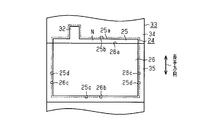
図4に示すように、負極電極24は、長尺帯状の電極材料33を図4の2点鎖線に沿ってレーザにより切断して製造される。電極材料33は、負極電極24の負極金属箔25を形成する長尺金属箔34と、長尺金属箔34の両面に設けられ、負極塗工部26を形成する負極活物質合剤の塗工部35とを備える。負極活物質合剤は、負極活物質、導電剤、及びバインダを混合したペースト状である。負極活物質合剤は、長尺金属箔34の長手方向に等間隔おきに塗布される。電極材料33の短手方向への寸法は、第1負極縁部25b及び第2負極縁部25cの寸法より長く、塗工部35は、電極材料33の短手方向の全体に亘って形成されている。そして、レーザ加工装置から照射されたレーザによって電極材料33を負極電極24の外形形状に切断する。
図4に示すように、負極電極24は、長尺帯状の電極材料33を図4の2点鎖線に沿ってレーザにより切断して製造される。電極材料33は、負極電極24の負極金属箔25を形成する長尺金属箔34と、長尺金属箔34の両面に設けられ、負極塗工部26を形成する負極活物質合剤の塗工部35とを備える。負極活物質合剤は、負極活物質、導電剤、及びバインダを混合したペースト状である。負極活物質合剤は、長尺金属箔34の長手方向に等間隔おきに塗布される。電極材料33の短手方向への寸法は、第1負極縁部25b及び第2負極縁部25cの寸法より長く、塗工部35は、電極材料33の短手方向の全体に亘って形成されている。そして、レーザ加工装置から照射されたレーザによって電極材料33を負極電極24の外形形状に切断する。
なお、図示しないが、本実施形態の正極電極21は、長尺帯状の電極材料を打ち抜き型により打ち抜いて製造される。正極電極21の製造に用いられる正極活物質合剤は、正極活物質、導電剤、及びバインダを混合したペースト状である。
図1又は図5に示すように、上記構成の正極電極21及び負極電極24は、それら正極電極21及び負極電極24の間にセパレータ27を挟んだ状態で積み重ねられ、電極組立体14を構成している。各正極電極21は、それぞれの正極タブ31が積層方向に沿って列状に配置されるように積層される。積層された状態の各正極タブ31は、第1正極縁部22b寄りの基端側から折り曲げられるとともに、折り曲げ部から先端に向かう方向が積層方向である。
同様に、各負極電極24は、それぞれの負極タブ32が、正極タブ31と重ならないように積層方向に沿って列状に配置されるように積層される。積層された状態の各負極タブ32は、第1負極縁部25b寄りの基端側から折り曲げられるとともに、折り曲げ部から先端に向かう方向が積層方向である。正極電極21と負極電極24は、正極タブ31と負極タブ32とが電極組立体14の同じ端面から同じ方向に突出している。そして、各正極電極21の正極タブ31は積層された状態で折り曲げられ、正極端子15と電気的に接続される。また、各負極電極24の負極タブ32も積層された状態で折り曲げられ、負極端子16と電気的に接続される。
電極組立体14は、正極塗工部23の全面に対し、セパレータ27を介して負極塗工部26が対向するように積層される必要がある。このため、負極塗工部26における高さH2は、正極塗工部23の高さH1より長く設定されている。
また、電極組立体14について、正極電極21及び負極電極24は、第1正極塗工縁部23aが第1負極塗工縁部26aよりも高さ方向下側に位置するように積層される。すなわち、第1負極塗工縁部26aは、第1正極塗工縁部23aよりも高さ方向一端側にある。言い換えると、正極電極21及び負極電極24は、第1正極縁部22bが第1負極縁部25bの下側に位置するように積層される。電極組立体14の底側では、正極電極21及び負極電極24は、第2正極塗工縁部23bが第2負極塗工縁部26bよりも高さ方向上側に位置するように積層される。言い換えると、正極電極21及び負極電極24は、第2正極縁部22cが第2負極縁部25cの上側に位置するように積層される。
ところで、正極電極21において、正極未塗工部Mは、高さHmについて設計時に設定された値(以下、中央値とする)を狙って製造される。しかし、様々な要因により、高さHmの実寸が中央値からずれる場合がある。要因は、正極電極21の製造に基づくものが多く、例えば活物質合剤の塗工時のずれ、活物質合剤が長尺金属箔34に対し片面ずつ別々に塗布されることを原因としたずれがある。上記のずれの中でも、打ち抜き場所のずれ等を原因とした打ち抜き時のずれと、活物質合剤が長尺金属箔34に対し片面ずつ別々に塗布されることを原因としたずれの2つのずれが発生しやすく、それらのずれが生じた結果として、中央値に対し1.0mmのずれが生じやすい。このため、本実施形態では、公差として最大1.0mm設定されている。
これらのずれが生じたとしても、正極未塗工部Mが形成されるように、正極未塗工部Mの高さHmは、中央値に、想定されるずれ量(以下、想定ずれ量xと記載する)よりも大きくした値を加えて設定されている。よって、正極未塗工部Mの高さHmには、設計上のずれ量が予め想定されている。
なお、想定ずれ量xには、高さHmの値が中央値よりも大きくなる場合と、高さHmの値が中央値よりも小さくなる場合とあるが、本実施形態では、想定ずれ量xを、高さHmの値が中央値よりも大きくなる場合として説明する。
設定した想定ずれ量xが大きいほど、第1正極縁部22bと第1正極塗工縁部23aとが離れ、正極未塗工部Mの高さHmの値は大きくなり、正極未塗工部Mは高くなる。一方、設定した想定ずれ量xが小さいほど、第1正極縁部22bと第1正極塗工縁部23aとが近付き、正極未塗工部Mの高さHmの値は小さくなり、正極未塗工部Mは低くなる。本実施形態では、想定ずれ量xを以下の式、
0<想定ずれ量x≦3mm
とした。想定ずれ量xがゼロより大きくなるように設定し、その想定ずれ量xに中央値を加味することで、ずれが生じても正極未塗工部Mは必ず形成されることとなる。正極未塗工部Mを備えた正極電極21では、その製造時、正極活物質合剤の塗工ずれ等が発生し、正極塗工部23の高さH1が中央値より大きくなっても正極活物質合剤は正極本体部22aに塗布され、正極塗工部23が形成される。よって、正極電極21の製造時、正極活物質合剤が正極タブ31となる位置に塗布されてしまうことを回避し、電池容量に寄与しない活物質が発生することを無くしている。
設定した想定ずれ量xが大きいほど、第1正極縁部22bと第1正極塗工縁部23aとが離れ、正極未塗工部Mの高さHmの値は大きくなり、正極未塗工部Mは高くなる。一方、設定した想定ずれ量xが小さいほど、第1正極縁部22bと第1正極塗工縁部23aとが近付き、正極未塗工部Mの高さHmの値は小さくなり、正極未塗工部Mは低くなる。本実施形態では、想定ずれ量xを以下の式、
0<想定ずれ量x≦3mm
とした。想定ずれ量xがゼロより大きくなるように設定し、その想定ずれ量xに中央値を加味することで、ずれが生じても正極未塗工部Mは必ず形成されることとなる。正極未塗工部Mを備えた正極電極21では、その製造時、正極活物質合剤の塗工ずれ等が発生し、正極塗工部23の高さH1が中央値より大きくなっても正極活物質合剤は正極本体部22aに塗布され、正極塗工部23が形成される。よって、正極電極21の製造時、正極活物質合剤が正極タブ31となる位置に塗布されてしまうことを回避し、電池容量に寄与しない活物質が発生することを無くしている。
また、想定ずれ量xを3mm以下に設定することで、正極未塗工部Mが必要以上に大きくなることを規制している。また、正極未塗工部Mの高さHmは、想定ずれ量xよりも1mm以下の範囲で大きくなるように設定されている。このように設定される正極未塗工部Mの高さHmは、具体的には0.5~2.0mmに設定されるのが好ましく、0.8~1.2mmに設定されるのがより好ましい。このように構成すると正極未塗工部Mの高さHmを公差1.0mmに近付けることができる。本実施形態では、正極電極21において、正極未塗工部MのHmは、1.2mmに設定されている。
一方、負極電極24について、負極塗工部26は、高さH2について設計時に設定された値(以下、中央値とする)を狙って製造される。しかし、様々な要因により、負極塗工部26の高さH2の実寸が中央値からずれる場合がある。要因は、負極電極24の製造に基づくものが多く、例えば活物質合剤の塗工時のずれ、活物質合剤が長尺金属箔34に対し片面ずつ別々に塗布されることを原因としたずれがある。これらのずれが生じたとしても、負極塗工部26が負極タブ32に形成されないように、負極塗工部26の高さH2は、想定されるずれ量(以下、想定ずれ量yと記載する)よりも大きく設定されている。よって、負極塗工部26の高さH2には、設計上のずれ量が予め想定されている。
なお、想定ずれ量yには、負極塗工部26の高さH2の値が中央値よりも大きくなる場合と、高さH2の値が中央値よりも小さくなる場合とあるが、本実施形態では、想定ずれ量yを、高さH2の値が中央値よりも大きくなる場合として説明する。
想定ずれ量yが大きいほど、第1負極塗工縁部26aと第1負極縁部25bとが近付き、負極塗工部26の高さH2の値は大きくなり、負極未塗工部Nは低くなる。そして、想定ずれ量yの最大値では、第1負極塗工縁部26aが第1負極縁部25bに一致し、負極未塗工部Nは形成されないが、負極タブ32には負極塗工部26が形成されない。一方、想定ずれ量yが小さいほど、第1負極塗工縁部26aと第1負極縁部25bとが離間し、負極塗工部26の高さH2の値は小さくなり、負極未塗工部Nは高くなる。
また、負極電極24の製造の際、設計上の中央値通りに負極活物質合剤が塗布され、しかも中央値通りに電極材料33が切断されると、負極電極24の第1負極縁部25bとなる部分の切断は、図4の2点鎖線に示すように、負極塗工部26の第1負極塗工縁部26aに平行な状態で長尺金属箔34を切断して行われる。このため、製造される負極電極24は、負極未塗工部Nを備えるとともに、負極未塗工部Nに沿う塗工部35の端縁そのものが第1負極塗工縁部26aとなる。なお、負極電極24の第2負極塗工縁部26b及び第3負極塗工縁部26cはレーザによって切断して形成される。
一方、負極電極24の製造の際、設計上の中央値通りに負極活物質合剤が塗布される一方で、設計上の中央値からずれて切断される場合がある。想定ずれ量yが最大の場合、すなわち、第1負極塗工縁部26aが第1負極縁部25b上に位置する場合は、負極電極24の第1負極縁部25bとなる部分の切断は、図6の2点鎖線に示すように、塗工部35に沿って長尺金属箔34を切断して行われる。このため、製造される負極電極24は、負極未塗工部Nは備えないが、塗工部35の端縁そのものが第1負極塗工縁部26aとなる。
次に、二次電池10の作用効果を記載する。
(1)負極電極24について、負極塗工部26の高さH2が設計上の中央値で製造された場合、第1負極塗工縁部26aは第1負極縁部25bよりも第2負極縁部25c寄りにあり、負極未塗工部Nが形成される。また、想定ずれ量yの最大値だけずれたとしても、設計上は、第1負極塗工縁部26aは第1負極縁部25b上に位置する。このため、電極材料33を切断して負極電極24を製造する際、負極タブ32の突出した第1負極縁部25bの形成のために塗工部35が切断されることはなく、塗工部35の切断に伴う負極活物質の脱落がない。よって、負極電極24が電極組立体14に組み込まれ、負極タブ32の突出した第1負極縁部25bが電極組立体14の上部に配置されても、第1負極縁部25bからの負極活物質の脱落を抑制でき、負極活物質が電極組立体14の層間に侵入することを回避できる。
(1)負極電極24について、負極塗工部26の高さH2が設計上の中央値で製造された場合、第1負極塗工縁部26aは第1負極縁部25bよりも第2負極縁部25c寄りにあり、負極未塗工部Nが形成される。また、想定ずれ量yの最大値だけずれたとしても、設計上は、第1負極塗工縁部26aは第1負極縁部25b上に位置する。このため、電極材料33を切断して負極電極24を製造する際、負極タブ32の突出した第1負極縁部25bの形成のために塗工部35が切断されることはなく、塗工部35の切断に伴う負極活物質の脱落がない。よって、負極電極24が電極組立体14に組み込まれ、負極タブ32の突出した第1負極縁部25bが電極組立体14の上部に配置されても、第1負極縁部25bからの負極活物質の脱落を抑制でき、負極活物質が電極組立体14の層間に侵入することを回避できる。
(2)電極材料33において、第1負極縁部25bの形成のための切断は、負極塗工部26が中央値で製造された場合、及び最大の想定ずれ量yずれて製造された場合のいずれであっても長尺金属箔34の切断である。このため、第1負極縁部25bを形成するための電極材料33の切断を塗工部35での切断とする場合と比べると、負極電極24の製造を容易かつ速やかに行うことができる。
(3)負極電極24において、想定ずれ量yが最大となった場合は、第1負極塗工縁部26aは第1負極縁部25b上にある。この場合であっても、負極塗工部26が負極タブ32に形成されることがなく、負極タブ32が積層された状態で折り曲げられても、負極塗工部26が負極タブ32の折り曲げの障害にならず、折り曲げに伴う負極活物質の脱落もない。
(4)想定ずれ量yが最大となる以外は、負極電極24は負極未塗工部Nを有する。二次電池10の組立工程において、電極組立体14をケース本体12内に挿入する際、電極組立体14は蓋体13によってケース本体12内に向けて押圧されることがある。このとき、負極電極24の負極未塗工部Nが蓋体13によって押圧され、負極塗工部26に蓋体13が接触することを規制でき、負極塗工部26からの負極活物質の脱落を抑止できる。また、負極未塗工部Nが撓むことで電極組立体14の底面がケース本体12の内底面に衝突することを抑止できる。
(5)正極未塗工部Mの高さHmを、中央値と、想定ずれ量xとの和の値よりも大きくした。このため、例えば、想定ずれ量xだけ第1正極縁部22bの位置が第2正極縁部22c側にずれたとしても、図3に示すように、第1正極縁部22bは2点鎖線T1に示す場所に位置し、正極未塗工部Mは確保される。また、想定ずれ量xだけ第1正極塗工縁部23aの位置が第1正極縁部22b側にずれたとしても、第1正極塗工縁部23aは2点鎖線T2に示す場所に位置し、正極未塗工部Mは確保される。そして、正極電極21において、正極未塗工部Mの想定ずれ量xを、0<想定ずれ量x≦3mm、とした。想定ずれ量xがゼロより大きくなるように設定することで、正極未塗工部Mを形成し、正極活物質合剤の塗布にずれが生じても正極未塗工部Mに塗工され、正極タブ31に正極塗工部23が形成されることを回避し、電池容量に寄与しない活物質が発生することを無くすことができる。また、想定最大ずれ量xを3mm以下に設定することで、正極未塗工部Mが必要以上に大きくなることを規制できる。
(6)正極電極21において、正極未塗工部Mの想定ずれ量xを、0<想定ずれ量x≦3mm、とした。想定ずれ量xがゼロより大きくなるように設定することで、正極未塗工部Mを形成できる。このため、電極材料33を切断して正極電極21を製造する際、正極タブ31の突出した第1正極縁部22bの形成のために塗工部35が切断されることはなく、塗工部35の切断に伴う正極活物質の脱落がない。よって、正極電極21が電極組立体14に組み込まれ、正極タブ31の突出した第1正極縁部22bが電極組立体14の上部に配置されても、第1正極縁部22bからの正極活物質の脱落を抑制でき、正極活物質が電極組立体14の層間に侵入することを回避できる。
(7)正極未塗工部Mの高さHmは、想定ずれ量xよりも1mm以下の範囲で大きくなるように設定されている。このため、想定ずれ量xだけずれが生じたとしても、正極未塗工部Mを確保できる。
(8)正極未塗工部Mの高さHmは、0.5~2.0mmに設定されるのが好ましく、0.8~1.2mmに設定されるのがより好ましい。このように構成すると正極未塗工部Mの高さHmを公差1.0mmに近付けることができる。
(9)正極タブ31は、第1正極縁部22b寄りの基端側から折り曲げられる。そして、正極電極21に正極未塗工部Mを形成することで、正極タブ31に正極塗工部23が形成されない。このため、正極タブ31に正極塗工部23が形成されている場合と比べると、正極タブ31を折り曲げときに、折り曲げ部に発生する応力を抑え、正極タブ31に亀裂等が入ることを抑制しやすくなる。
(10)負極タブ32は、第1負極縁部25b寄りの基端側から折り曲げられる。そして、負極電極24に負極未塗工部Nを形成することで、負極タブ32に負極塗工部26が形成されない。このため、負極タブ32に負極塗工部26が形成されている場合と比べると、負極タブ32を折り曲げときに、折り曲げ部に発生する応力を抑え、負極タブ32に亀裂等が入ることを抑制しやすくなる。
なお、本実施形態は以下のように変更してもよい。
○ 負極電極24の製造のために行う電極材料33の切断は、レーザでなく、打ち抜きでもよい。
○ 負極電極24の製造のために行う電極材料33の切断は、レーザでなく、打ち抜きでもよい。
○ 上記構成を有する正極電極21と負極電極24であれば、正極タブ31の突出する向きと、負極タブ32が突出する向きが異なるように積層されていても、実施形態と同様の作用効果を奏する。
○ 二次電池10は、リチウムイオン二次電池であったが、これに限らず、他の二次電池であってもよい。要するに、正極活物質と負極活物質との間をイオンが移動するとともに電荷の授受を行うものであればよい。
○ 正極集電体として正極金属箔22に具体化し、負極集電体として負極金属箔25に具体化したが、塗工部を保持できれば集電体は金属箔以外のシート体であってもよい。
○ 電気二重層キャパシタ等の蓄電装置に具体化してもよい。
○ 電気二重層キャパシタ等の蓄電装置に具体化してもよい。
次に、上記実施形態及び別例から把握できる技術的思想について以下に追記する。
(1)前記正極集電体及び前記負極集電体は金属箔である。
(2)前記電極組立体の端面に前記正極タブ及び前記負極タブが存在する。
(1)前記正極集電体及び前記負極集電体は金属箔である。
(2)前記電極組立体の端面に前記正極タブ及び前記負極タブが存在する。
M…正極未塗工部、10…蓄電装置としての二次電池、14…電極組立体、21…正極電極、22…正極集電体としての正極金属箔、22a…正極本体部、22b…第1正極縁部、22c…第2正極縁部、23…正極塗工部、24…負極電極、25…負極集電体としての負極金属箔、25a…負極本体部、25b…第1負極縁部、25c…第2負極縁部、26…負極塗工部、26a…第1負極塗工縁部、31…正極タブ、32…負極タブ。
Claims (6)
- 複数の正極電極と複数の負極電極とが互いに絶縁された状態で交互に積層された電極組立体を有する蓄電装置であって、
前記正極電極は、正極集電体を備えるとともに、該正極集電体は矩形状の正極本体部と、該正極本体部の第1正極縁部の一部から突出した形状の正極タブと、を備え、かつ前記正極本体部の前記第1正極縁部の対辺となる第2正極縁部を有し、
前記正極本体部の表面に正極活物質合剤を塗布して形成された正極塗工部と、前記第1正極縁部に沿って正極活物質合剤が塗布されず前記正極本体部の露出した正極未塗工部とを備え、
前記正極電極において、前記第1正極縁部と前記第2正極縁部とを最短距離で結ぶ直線の延びる方向を高さ方向とし、該高さ方向への前記正極未塗工部の寸法を高さとし、前記正極未塗工部の高さにおいて、設計上、想定されるずれ量を想定ずれ量とすると、
前記正極未塗工部の高さは、設計上設定された中央値と、前記想定ずれ量よりも大きく設定された値との和であり、前記想定ずれ量は、以下の式、
0<想定ずれ量≦3mm
が成立し、
前記正極塗工部の高さ方向一端に位置し、かつ前記第1正極縁部側の縁部を正極塗工縁部とし、
前記負極電極は、負極集電体を備えるとともに、該負極集電体は矩形状の負極本体部と、該負極本体部の第1負極縁部の一部から突出した形状の負極タブと、を備え、かつ前記負極本体部の前記第1負極縁部の対辺となる第2負極縁部を有し、
前記負極本体部の表面に負極活物質合剤を塗布して形成された負極塗工部を備え、
前記負極電極は、前記第1負極縁部と前記第2負極縁部とを最短距離で結ぶ直線の延びる方向を高さ方向とし、前記負極塗工部の高さ方向一端に位置し、かつ前記第1負極縁部側の縁部を第1負極塗工縁部とした場合、
前記第1負極塗工縁部は、設計上、前記第1負極縁部上、又は前記第1負極縁部よりも前記第2負極縁部寄りにあり、かつ前記正極塗工縁部より前記高さ方向一端側に位置することを特徴とする蓄電装置。 - 前記第1負極塗工縁部は、前記第1負極縁部と一致している請求項1に記載の蓄電装置。
- 前記正極未塗工部において、前記想定ずれ量よりも大きくする範囲は1.0mm以下である請求項1又は請求項2に記載の蓄電装置。
- 複数の正極電極と複数の負極電極とが互いに絶縁された状態で交互に積層された電極組立体を有する蓄電装置であって、
前記正極電極は、正極集電体を備えるとともに、該正極集電体は矩形状の正極本体部と、該正極本体部の第1正極縁部の一部から突出した形状の正極タブと、を備え、かつ前記正極本体部の前記第1正極縁部の対辺となる第2正極縁部を有し、
前記正極本体部の表面に正極活物質合剤を塗布して形成された正極塗工部と、前記第1正極縁部に沿って正極活物質合剤が塗布されず前記正極本体部の露出した正極未塗工部とを備え、
前記正極電極において、前記第1正極縁部と前記第2正極縁部とを最短距離で結ぶ直線の延びる方向を高さ方向とし、該高さ方向への前記正極未塗工部の寸法を高さとし、前記正極未塗工部の高さは、0.5~2.0mmであり、
前記正極塗工部の高さ方向一端に位置し、かつ前記第1正極縁部側の縁部を正極塗工縁部とし、
前記負極電極は、負極集電体を備えるとともに、該負極集電体は矩形状の負極本体部と、該負極本体部の第1負極縁部の一部から突出した形状の負極タブと、を備え、かつ前記負極本体部の前記第1負極縁部の対辺となる第2負極縁部を有し、
前記負極本体部の表面に負極活物質合剤を塗布して形成された負極塗工部を備え、
前記負極電極は、前記第1負極縁部と前記第2負極縁部とを最短距離で結ぶ直線の延びる方向を高さ方向とし、前記負極塗工部の高さ方向一端に位置し、かつ前記第1負極縁部側の縁部を第1負極塗工縁部とした場合、
前記第1負極塗工縁部は、設計上、前記第1負極縁部上、又は前記第1負極縁部よりも前記第2負極縁部寄りにあり、かつ前記正極塗工縁部より前記高さ方向一端側に位置することを特徴とする蓄電装置。 - 前記正極未塗工部の高さは、0.8~1.2mmである請求項4に記載の蓄電装置。
- 前記正極タブは、前記第1正極縁部寄りの基端側から折り曲げられるとともに、折り曲げ部から先端に向かう方向が前記正極電極と前記負極電極の積層方向である請求項1~請求項5のうちのいずれか一項に記載の蓄電装置。
Applications Claiming Priority (2)
| Application Number | Priority Date | Filing Date | Title |
|---|---|---|---|
| JP2017-036917 | 2017-02-28 | ||
| JP2017036917 | 2017-02-28 |
Publications (1)
| Publication Number | Publication Date |
|---|---|
| WO2018159078A1 true WO2018159078A1 (ja) | 2018-09-07 |
Family
ID=63369908
Family Applications (1)
| Application Number | Title | Priority Date | Filing Date |
|---|---|---|---|
| PCT/JP2017/045845 Ceased WO2018159078A1 (ja) | 2017-02-28 | 2017-12-21 | 蓄電装置 |
Country Status (1)
| Country | Link |
|---|---|
| WO (1) | WO2018159078A1 (ja) |
Citations (4)
| Publication number | Priority date | Publication date | Assignee | Title |
|---|---|---|---|---|
| JP2006156000A (ja) * | 2004-11-26 | 2006-06-15 | Nissan Motor Co Ltd | バイポーラ電池およびその製造方法、組電池、自動車 |
| JP2013161756A (ja) * | 2012-02-08 | 2013-08-19 | Toyota Industries Corp | 蓄電装置及び車両 |
| JP2013175407A (ja) * | 2012-02-27 | 2013-09-05 | Toyota Industries Corp | 蓄電装置、車両 |
| JP2016009547A (ja) * | 2014-06-23 | 2016-01-18 | 株式会社デンソー | 電池 |
-
2017
- 2017-12-21 WO PCT/JP2017/045845 patent/WO2018159078A1/ja not_active Ceased
Patent Citations (4)
| Publication number | Priority date | Publication date | Assignee | Title |
|---|---|---|---|---|
| JP2006156000A (ja) * | 2004-11-26 | 2006-06-15 | Nissan Motor Co Ltd | バイポーラ電池およびその製造方法、組電池、自動車 |
| JP2013161756A (ja) * | 2012-02-08 | 2013-08-19 | Toyota Industries Corp | 蓄電装置及び車両 |
| JP2013175407A (ja) * | 2012-02-27 | 2013-09-05 | Toyota Industries Corp | 蓄電装置、車両 |
| JP2016009547A (ja) * | 2014-06-23 | 2016-01-18 | 株式会社デンソー | 電池 |
Similar Documents
| Publication | Publication Date | Title |
|---|---|---|
| JP7662007B2 (ja) | 蓄電素子 | |
| JP6657843B2 (ja) | 二次電池 | |
| JP5392368B2 (ja) | 蓄電装置 | |
| CN104137319B (zh) | 蓄电装置以及搭载了该蓄电装置的车辆 | |
| JP6769137B2 (ja) | 蓄電装置 | |
| USRE50254E1 (en) | Electrode assembly including electrode plates with electrode plate extensions | |
| WO2014027606A1 (ja) | 蓄電装置 | |
| KR102071622B1 (ko) | 전극조립체 및 이를 포함하는 이차전지 | |
| JP2017076478A (ja) | 折り畳み式二次電池 | |
| CN106328843B (zh) | 二次电池 | |
| JP2019121433A (ja) | 蓄電装置 | |
| KR20190101372A (ko) | 배터리 셀 및 배터리 셀의 제조 방법 | |
| JP6287563B2 (ja) | 蓄電装置 | |
| JP6729309B2 (ja) | 蓄電装置 | |
| JP5621750B2 (ja) | 二次電池および二次電池を搭載した車両 | |
| KR20170050444A (ko) | 파우치형 이차전지 | |
| JP7600978B2 (ja) | 電池 | |
| JP5845706B2 (ja) | 二次電池とその製造方法 | |
| JP2018142513A (ja) | 蓄電装置 | |
| JP2020013706A (ja) | 蓄電装置及び蓄電装置の製造方法 | |
| JP6229430B2 (ja) | 積層型電池 | |
| JP2018060699A (ja) | 積層型二次電池の製造方法 | |
| JP2018113190A (ja) | 積層型二次電池の製造方法 | |
| WO2019123588A1 (ja) | 蓄電装置 | |
| JP2016085844A (ja) | 蓄電装置 |
Legal Events
| Date | Code | Title | Description |
|---|---|---|---|
| 121 | Ep: the epo has been informed by wipo that ep was designated in this application |
Ref document number: 17898514 Country of ref document: EP Kind code of ref document: A1 |
|
| NENP | Non-entry into the national phase |
Ref country code: DE |
|
| 122 | Ep: pct application non-entry in european phase |
Ref document number: 17898514 Country of ref document: EP Kind code of ref document: A1 |
|
| NENP | Non-entry into the national phase |
Ref country code: JP |