WO2018154880A1 - Method for manufacturing product, exterior component, and device for selecting antenna pattern - Google Patents
Method for manufacturing product, exterior component, and device for selecting antenna pattern Download PDFInfo
- Publication number
- WO2018154880A1 WO2018154880A1 PCT/JP2017/041271 JP2017041271W WO2018154880A1 WO 2018154880 A1 WO2018154880 A1 WO 2018154880A1 JP 2017041271 W JP2017041271 W JP 2017041271W WO 2018154880 A1 WO2018154880 A1 WO 2018154880A1
- Authority
- WO
- WIPO (PCT)
- Prior art keywords
- antenna
- resin molded
- chip
- product
- antenna wiring
- Prior art date
Links
Images


Classifications
-
- G—PHYSICS
- G06—COMPUTING; CALCULATING OR COUNTING
- G06K—GRAPHICAL DATA READING; PRESENTATION OF DATA; RECORD CARRIERS; HANDLING RECORD CARRIERS
- G06K19/00—Record carriers for use with machines and with at least a part designed to carry digital markings
- G06K19/06—Record carriers for use with machines and with at least a part designed to carry digital markings characterised by the kind of the digital marking, e.g. shape, nature, code
- G06K19/067—Record carriers with conductive marks, printed circuits or semiconductor circuit elements, e.g. credit or identity cards also with resonating or responding marks without active components
- G06K19/07—Record carriers with conductive marks, printed circuits or semiconductor circuit elements, e.g. credit or identity cards also with resonating or responding marks without active components with integrated circuit chips
- G06K19/077—Constructional details, e.g. mounting of circuits in the carrier
- G06K19/0772—Physical layout of the record carrier
- G06K19/07724—Physical layout of the record carrier the record carrier being at least partially made by a molding process
-
- H—ELECTRICITY
- H01—ELECTRIC ELEMENTS
- H01Q—ANTENNAS, i.e. RADIO AERIALS
- H01Q1/00—Details of, or arrangements associated with, antennas
- H01Q1/36—Structural form of radiating elements, e.g. cone, spiral, umbrella; Particular materials used therewith
- H01Q1/38—Structural form of radiating elements, e.g. cone, spiral, umbrella; Particular materials used therewith formed by a conductive layer on an insulating support
-
- G—PHYSICS
- G06—COMPUTING; CALCULATING OR COUNTING
- G06K—GRAPHICAL DATA READING; PRESENTATION OF DATA; RECORD CARRIERS; HANDLING RECORD CARRIERS
- G06K19/00—Record carriers for use with machines and with at least a part designed to carry digital markings
- G06K19/06—Record carriers for use with machines and with at least a part designed to carry digital markings characterised by the kind of the digital marking, e.g. shape, nature, code
- G06K19/067—Record carriers with conductive marks, printed circuits or semiconductor circuit elements, e.g. credit or identity cards also with resonating or responding marks without active components
- G06K19/07—Record carriers with conductive marks, printed circuits or semiconductor circuit elements, e.g. credit or identity cards also with resonating or responding marks without active components with integrated circuit chips
- G06K19/077—Constructional details, e.g. mounting of circuits in the carrier
- G06K19/0772—Physical layout of the record carrier
- G06K19/07728—Physical layout of the record carrier the record carrier comprising means for protection against impact or bending, e.g. protective shells or stress-absorbing layers around the integrated circuit
Landscapes
- Engineering & Computer Science (AREA)
- Computer Hardware Design (AREA)
- Microelectronics & Electronic Packaging (AREA)
- Physics & Mathematics (AREA)
- General Physics & Mathematics (AREA)
- Theoretical Computer Science (AREA)
- Details Of Aerials (AREA)
- Credit Cards Or The Like (AREA)
Abstract
This method for manufacturing a relay is provided with: a resin molding step for injecting a resin so that the resin surrounds an IC chip (12) thereby molding a resin molding (11) in which the IC chip (12) is embedded; an assembly step for attaching the resin molding (11), as an exterior component (10) for a relay, to a base member (20) that is a body of the relay; and an antenna wiring forming step for printing, on a surface (11a) of the resin molding (11), an antenna wiring (13) for the IC chip (12) to perform wireless communication. As a result, a product provided with an IC tag having an antenna pattern selected from multiple types of antenna patterns, can be manufactured easily in a short time after receiving an order.
Description
本技術は、無線通信可能なICチップを備えた製品の製造方法、その製品の外装部品およびアンテナパターン選択装置に関する。
The present technology relates to a manufacturing method of a product including an IC chip capable of wireless communication, an exterior component of the product, and an antenna pattern selection device.
近年、各種製品の寿命もしくは修復履歴の管理、または製品が設置されている環境等をの監視の目的で、製品単体毎の識別情報を把握する需要が高まっている。たとえば、生産工場において使用されている装置に内装されている部品の識別情報を把握する需要がある。
In recent years, there has been an increasing demand for grasping identification information for each product for the purpose of managing the life or repair history of various products or monitoring the environment where the product is installed. For example, there is a demand for grasping identification information of a part built in an apparatus used in a production factory.
こうした需要への対応として、バーコードまたは2次元コードを示すラベルを製品に貼付することが従来から行われている。しかしながら、コードを読み取る際にはリーダをラベルに対向させる必要がある。そのため、装置の内部に実装される製品(部品)あるいは密集状態で実装されている製品(部品)にアクセスすることが困難となる。
In response to such demand, it has been conventionally practiced to attach a label indicating a barcode or a two-dimensional code to a product. However, when reading the code, the reader needs to face the label. Therefore, it becomes difficult to access a product (component) mounted in the apparatus or a product (component) mounted in a dense state.
こうした問題を解決する方法として、たとえばUHF帯の電波を用いて非接触で通信することが可能なIC(Integrated Circuit)タグを用いる方法が知られている。ICタグとリーダとは、電波でのデータ通信が可能である。そのため、リーダは、ICタグと対向していなくても、ICタグから識別情報を読み取ることができる。
As a method for solving such a problem, for example, a method using an IC (Integrated Circuit) tag capable of contactless communication using radio waves in the UHF band is known. The IC tag and the reader can perform data communication using radio waves. Therefore, the reader can read the identification information from the IC tag even if it is not opposed to the IC tag.
一般的なICタグは、PET(ポリエチレンテレフタレート)あるいはポリイミドのフィルム上に銅箔等のエッチングあるいは銀等の導電ペーストのスクリーン印刷によって形成されたアンテナと、ICチップとによって構成される。ICタグは、接着剤等により製品に貼付される方法で使用されている。
A general IC tag includes an antenna formed on a PET (polyethylene terephthalate) or polyimide film by etching copper foil or screen printing of a conductive paste such as silver, and an IC chip. An IC tag is used by a method of being attached to a product with an adhesive or the like.
ところで、ICタグとして使用可能な周波数は、国によって異なる。そのため、製品が出荷される国に合わせて、アンテナの共振周波数を調整する必要がある。特開2007-96768号公報(特許文献1)には、アンテナに対するICチップの接続位置を変更することにより、周波数帯域の異なるICタグを製造する方法が開示されている。特開2005-301443号公報(特許文献2)には、複数の回路要素をあらかじめ形成しておき、必要な周波数に合わせて不要な回路要素を焼切る方法が開示されている。
By the way, the frequencies that can be used as IC tags differ from country to country. Therefore, it is necessary to adjust the resonance frequency of the antenna according to the country where the product is shipped. Japanese Unexamined Patent Application Publication No. 2007-96768 (Patent Document 1) discloses a method of manufacturing IC tags having different frequency bands by changing the connection position of an IC chip with respect to an antenna. Japanese Patent Laying-Open No. 2005-301443 (Patent Document 2) discloses a method in which a plurality of circuit elements are formed in advance and unnecessary circuit elements are burned out in accordance with a required frequency.
ICタグを構成するICチップは、機械的負荷に対して非常に脆く、破損し易い。そのため、特開2008-210344号公報(特許文献3)には、ICタグ全体を樹脂材あるいはゴム材等に埋め込んでICチップを保護する技術が開示されている。特開2000-294577号公報(特許文献4)および特開2002-261421号公報(特許文献5)には、ICチップを平板状の基板に埋め込み、露出させたICチップの電極に接続するようにアンテナを形成してICタグを構成する技術が開示されている。
The IC chip constituting the IC tag is very fragile to mechanical loads and easily damaged. Therefore, Japanese Patent Application Laid-Open No. 2008-210344 (Patent Document 3) discloses a technique for protecting an IC chip by embedding an entire IC tag in a resin material or a rubber material. In Japanese Patent Laid-Open No. 2000-294577 (Patent Document 4) and Japanese Patent Laid-Open No. 2002-261421 (Patent Document 5), an IC chip is embedded in a flat substrate and connected to the exposed electrode of the IC chip. A technique for forming an antenna to form an IC tag is disclosed.
しかしながら、特開2007-96768号公報に記載の技術では、アンテナとICチップとの接続位置により周波数帯域を調整するため、調整可能な範囲が限られる。さらに、必要な通信距離に応じてアンテナの形態(たとえば、パッチアンテナ、ループアンテナなど)を変更することができない。そのため、製品が出荷される国の周波数規格や必要な通信距離などに合わせたアンテナを有するICタグを事前に複数個在庫しておく必要があり、製造コストが増加する。特開2005-301443号公報に記載の技術でも同様の問題がある。
However, in the technique described in Japanese Patent Application Laid-Open No. 2007-96768, the adjustable range is limited because the frequency band is adjusted according to the connection position between the antenna and the IC chip. Furthermore, the form of the antenna (for example, a patch antenna, a loop antenna, etc.) cannot be changed according to the required communication distance. Therefore, it is necessary to stock a plurality of IC tags having antennas in accordance with the frequency standard of the country to which the product is shipped and the necessary communication distance, and the manufacturing cost increases. The technique described in Japanese Patent Laid-Open No. 2005-301443 has the same problem.
特開2008-210344号公報、特開2000-294577号公報および特開2002-261421号公報に記載の技術によって製造されたICタグは、一般には製品の内部に搭載される。そのため、製品の出荷先が決定されてから、当該出荷先に応じた共振周波数を有するアンテナを備えたICタグを準備し、当該ICタグを用いた製品の組み立てを開始する必要がある。よって、受注してから製品が完成するまでに時間がかかる。
IC tags manufactured by the techniques described in JP 2008-210344 A, JP 2000-294577 A, and JP 2002-261421 A are generally mounted inside products. For this reason, after the shipment destination of the product is determined, it is necessary to prepare an IC tag including an antenna having a resonance frequency corresponding to the shipment destination, and to start assembling the product using the IC tag. Therefore, it takes time until the product is completed after receiving an order.
本発明は、上記の問題点に着目してなされたもので、多種類のアンテナパターンから選択されたアンテナパターンを有するICタグを備えた製品を、受注してから短時間で容易に製造することができる製品の製造方法、その製品の外装部品およびアンテナパターン選択装置を提供することを目的としている。
The present invention has been made paying attention to the above problems, and can easily manufacture a product including an IC tag having an antenna pattern selected from a variety of antenna patterns in a short time after receiving an order. It is an object of the present invention to provide a method for manufacturing a product, an exterior part of the product, and an antenna pattern selection device.
ある局面に従うと、製品の製造方法は、製品を識別するための識別データを記憶するICチップを囲むように樹脂を射出することにより、ICチップを埋設した樹脂成形体を成形する第1工程と、樹脂成形体を製品の外装部品として、製品本体に取り付ける第2工程と、製品本体に取り付けられた樹脂成形体の外表面上に、ICチップが無線通信するためのアンテナ配線を印刷する第3工程とを備える。
According to a certain aspect, a manufacturing method of a product includes a first step of molding a resin molded body in which an IC chip is embedded by injecting a resin so as to surround an IC chip that stores identification data for identifying the product. The second step of attaching the resin molded body to the product body as an exterior part of the product, and the third step of printing the antenna wiring for wireless communication of the IC chip on the outer surface of the resin molded body attached to the product body A process.
好ましくは、製品の製造方法は、製品の出荷先の周波数規格および製品の使用環境の少なくとも一方に応じて、アンテナ配線のパターンを決定する第4工程をさらに備える。第3工程において、第4工程によって決定されたパターンのアンテナ配線を印刷する。
Preferably, the product manufacturing method further includes a fourth step of determining an antenna wiring pattern according to at least one of a frequency standard of a product shipping destination and a use environment of the product. In the third step, the antenna wiring having the pattern determined in the fourth step is printed.
別の局面に従うと、製品の外装部品は、樹脂成形体を備える。樹脂成形体の表面は、外装部品の外表面となる第1面を含む。外装部品は、樹脂成形体に埋設され、製品を識別する識別データを記憶するICチップと、第1面の上に形成された、ICチップが無線通信するためのアンテナ配線とをさらに備える。
According to another situation, the exterior part of the product is provided with a resin molded body. The surface of the resin molded body includes a first surface serving as an outer surface of the exterior component. The exterior component further includes an IC chip that is embedded in the resin molded body and stores identification data for identifying a product, and an antenna wiring that is formed on the first surface and for wireless communication with the IC chip.
好ましくは、外装部品は、アンテナ配線の上に形成された絶縁膜をさらに備える。
好ましくは、ICチップは、第1面から露出する。アンテナ配線は、ICチップに電気的に接続される。 Preferably, the exterior component further includes an insulating film formed on the antenna wiring.
Preferably, the IC chip is exposed from the first surface. The antenna wiring is electrically connected to the IC chip.
好ましくは、ICチップは、第1面から露出する。アンテナ配線は、ICチップに電気的に接続される。 Preferably, the exterior component further includes an insulating film formed on the antenna wiring.
Preferably, the IC chip is exposed from the first surface. The antenna wiring is electrically connected to the IC chip.
好ましくは、外装部品は、ICチップに接続されたIC側アンテナをさらに備える。ICチップとIC側アンテナとは、一体化されてICモジュールを構成する。樹脂成形体は、ICモジュールを埋設する。アンテナ配線は、IC側アンテナと電磁結合するブースターアンテナである。
Preferably, the exterior component further includes an IC side antenna connected to the IC chip. The IC chip and the IC side antenna are integrated to form an IC module. The resin molded body embeds the IC module. The antenna wiring is a booster antenna that is electromagnetically coupled to the IC side antenna.
好ましくは、樹脂成形体の表面は、外装部品の内表面となる第2面を含む。第2面は、第1面の裏側の面である。ICモジュールは、第2面から露出するように樹脂成形体に埋設される。アンテナ配線は、ICモジュールに対向するように第1面の上に形成される。
Preferably, the surface of the resin molded body includes a second surface serving as an inner surface of the exterior part. The second surface is a surface on the back side of the first surface. The IC module is embedded in the resin molded body so as to be exposed from the second surface. The antenna wiring is formed on the first surface so as to face the IC module.
あるいは、樹脂成形体は、第1樹脂成形部品と第2樹脂成形部品とを含んでもよい。第1面は、第1樹脂成形部品の外表面の一部である。第2樹脂成形部品の外表面は、第1面と同一平面上にある第2面を含む。ICモジュールは、第2樹脂成形部品に埋設され、第2面から露出する。
Alternatively, the resin molded body may include a first resin molded part and a second resin molded part. The first surface is a part of the outer surface of the first resin molded part. The outer surface of the second resin molded part includes a second surface that is coplanar with the first surface. The IC module is embedded in the second resin molded part and exposed from the second surface.
別の局面に従うと、上記の外装部品におけるアンテナ配線のパターンを選択するアンテナパターン選択装置は、製品の出荷先を示す出荷先情報の入力を受ける第1入力部と、製品の使用環境を示す環境情報の入力を受ける第2入力部と、環境情報によって示される使用環境に基づいて、アンテナ配線の通信条件を設定する通信条件設定部と、出荷先および通信条件とアンテナ配線のパターンとを対応付けた情報に基づいて、出荷先情報によって示される出荷先と、通信条件設定部によって設定された通信条件に対応するアンテナ配線のパターンを選択するパターン選択部とを備える。
According to another aspect, an antenna pattern selection device that selects a pattern of antenna wiring in the exterior part described above includes a first input unit that receives input of shipping destination information indicating a shipping destination of a product, and an environment that indicates a usage environment of the product. The second input unit that receives information input, the communication condition setting unit that sets the antenna wiring communication conditions based on the use environment indicated by the environmental information, and the shipping destination, communication conditions, and antenna wiring pattern are associated with each other. Based on the received information, a shipping destination indicated by the shipping destination information, and a pattern selection unit for selecting an antenna wiring pattern corresponding to the communication condition set by the communication condition setting unit.
本開示によれば、多種類のアンテナパターンから選択されたアンテナパターンを有するICタグを備えた製品を、受注してから短時間で容易に製造することができる。
According to the present disclosure, a product including an IC tag having an antenna pattern selected from a variety of antenna patterns can be easily manufactured in a short time after receiving an order.
本発明の実施の形態について、図面を参照しながら詳細に説明する。なお、図中の同一または相当部分については、同一符号を付してその説明は繰返さない。また、以下で説明する各実施の形態または変形例は、適宜選択的に組み合わされてもよい。
Embodiments of the present invention will be described in detail with reference to the drawings. Note that the same or corresponding parts in the drawings are denoted by the same reference numerals and description thereof will not be repeated. Each embodiment or modification described below may be selectively combined as appropriate.
以下では、外装部品の一例として、リレーの外装部品を説明する。ただし、外装部品は、リレーの外装部品に限定されるものではなく、その他の製品(たとえば、インクカートリッジなど)の外装部品であってもよい。
Hereinafter, a relay exterior part will be described as an example of the exterior part. However, the exterior part is not limited to the exterior part of the relay, and may be an exterior part of another product (for example, an ink cartridge).
<実施の形態1>
(リレーの構造)
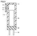
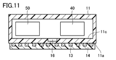
図1~図3を参照して、実施の形態1に係る外装部品10を備えたリレー(製品)1の概略的な構成について説明する。図1は、実施の形態1に係るリレー1を示す正面図である。図2は、図1のX-X線に沿った矢視断面図である。図3は、図1のXI-XI線に沿った矢視断面図である。 <Embodiment 1>
(Relay structure)
A schematic configuration of a relay (product) 1 including theexterior component 10 according to the first embodiment will be described with reference to FIGS. FIG. 1 is a front view showing a relay 1 according to the first embodiment. FIG. 2 is a cross-sectional view taken along the line XX of FIG. 3 is a cross-sectional view taken along the line XI-XI in FIG.
(リレーの構造)
図1~図3を参照して、実施の形態1に係る外装部品10を備えたリレー(製品)1の概略的な構成について説明する。図1は、実施の形態1に係るリレー1を示す正面図である。図2は、図1のX-X線に沿った矢視断面図である。図3は、図1のXI-XI線に沿った矢視断面図である。 <
(Relay structure)
A schematic configuration of a relay (product) 1 including the
図1~図3に示されるように、リレー1は、外装部品10と、ベース部材20と、複数の端子30と、電磁石40と、接点部50とを備える。ベース部材20と、複数の端子30と、電磁石40と、接点部50とにより、リレー1の本体(製品本体)が構成される。
1 to 3, the relay 1 includes an exterior component 10, a base member 20, a plurality of terminals 30, an electromagnet 40, and a contact portion 50. The base member 20, the plurality of terminals 30, the electromagnet 40, and the contact portion 50 constitute a main body (product main body) of the relay 1.
電磁石40および接点部50は、平板上のベース部材20の一方の面上に実装される。複数の端子30の各々は、電磁石40または接点部50に接続され、ベース部材20を貫通して、ベース部材20の他方の面から突出する。
The electromagnet 40 and the contact portion 50 are mounted on one surface of the base member 20 on a flat plate. Each of the plurality of terminals 30 is connected to the electromagnet 40 or the contact portion 50, passes through the base member 20, and protrudes from the other surface of the base member 20.
接点部50は、固定接点と可動接点とから構成される。電磁石40のコイルに接続された端子30に通電すると、電磁石40の磁力によって図示しない鉄片が移動する。可動接点は、当該鉄片の移動に伴って固定接点側に移動し、固定接点と電気的に接続する。電磁石40のコイルへの通電を止めると、可動接点は、弾性力によって固定接点から離れる方向に移動する。これにより、可動接点は、固定接点と電気的に非接続となる。
The contact part 50 is composed of a fixed contact and a movable contact. When the terminal 30 connected to the coil of the electromagnet 40 is energized, an iron piece (not shown) is moved by the magnetic force of the electromagnet 40. The movable contact moves to the fixed contact side as the iron piece moves, and is electrically connected to the fixed contact. When energization of the coil of the electromagnet 40 is stopped, the movable contact moves in a direction away from the fixed contact by elastic force. Thereby, the movable contact is electrically disconnected from the fixed contact.
外装部品10は、電磁石40および接点部50を覆う、箱状のカバーである。外装部品10の開口端は、ベース部材20における電磁石40および接点部50が実装された面に接合する。これにより、外装部品10の内部の空間に電磁石40および接点部50が収容される。なお、外装部品10の形状は、特に限定されるものではない。
The exterior component 10 is a box-shaped cover that covers the electromagnet 40 and the contact portion 50. The open end of the exterior component 10 is joined to the surface of the base member 20 on which the electromagnet 40 and the contact portion 50 are mounted. Thereby, the electromagnet 40 and the contact part 50 are accommodated in the space inside the exterior component 10. Note that the shape of the exterior component 10 is not particularly limited.
(外装部品の構造)
図1~図3に示されるように、外装部品10は、樹脂成形体11と、ICチップ12と、アンテナ配線13と、絶縁膜14とを備える。 (Structure of exterior parts)
As shown in FIGS. 1 to 3, theexterior component 10 includes a resin molded body 11, an IC chip 12, an antenna wiring 13, and an insulating film 14.
図1~図3に示されるように、外装部品10は、樹脂成形体11と、ICチップ12と、アンテナ配線13と、絶縁膜14とを備える。 (Structure of exterior parts)
As shown in FIGS. 1 to 3, the
ICチップ12は、リレー1を識別する識別データを記憶し、外部からの要求に応じて当該識別データを出力する。識別データは、ICチップ12と外部のリーダとの間の認証用に使用される。識別データには、リレー1の個体番号の他に、リレー1の仕様、特性、製造日などの各種情報が含まれる。
The IC chip 12 stores identification data for identifying the relay 1 and outputs the identification data in response to an external request. The identification data is used for authentication between the IC chip 12 and an external reader. In addition to the individual number of the relay 1, the identification data includes various information such as the specifications, characteristics, and date of manufacture of the relay 1.
樹脂成形体11は、外装部品10の本体となる箱状の部材であり、ポリカーボネイト(PC)やアクリロニトリルブタジエンスチレン(ABS)、ポリプロピレン(PP)等の樹脂からなる。樹脂成形体11の形状は、特に限定されるものではなく、リレー1に合わせて適宜設計される。樹脂成形体11の材質も特に限定されるものではない。
The resin molded body 11 is a box-shaped member that becomes the main body of the exterior component 10 and is made of a resin such as polycarbonate (PC), acrylonitrile butadiene styrene (ABS), or polypropylene (PP). The shape of the resin molded body 11 is not particularly limited, and is appropriately designed according to the relay 1. The material of the resin molding 11 is not particularly limited.
樹脂成形体11の表面は、外装部品10の外表面となる面11aを含む。面11aは、箱状の樹脂成形体11の4つの側面のうち最も面積の大きい面である。
The surface of the resin molded body 11 includes a surface 11 a that is an outer surface of the exterior component 10. The surface 11 a is the surface having the largest area among the four side surfaces of the box-shaped resin molded body 11.
樹脂成形体11は、ICチップ12が面11aから露出するように、ICチップ12を埋設する。ICチップ12における樹脂成形体11から露出する面には、アンテナ配線13を接続するための端子が形成されている。
The resin molded body 11 embeds the IC chip 12 so that the IC chip 12 is exposed from the surface 11a. Terminals for connecting the antenna wiring 13 are formed on the surface of the IC chip 12 exposed from the resin molded body 11.
アンテナ配線13は、樹脂成形体11の面11aの上に形成され、ICチップ12の端子と電気的に接続される導電回路である。アンテナ配線13は、インクジェット印刷法を用いて銀(Ag)インクを噴射することにより、容易に形成することができる。インクジェット印刷法は、インクをノズルから噴射し、インクを噴射対象面上に堆積させる印刷方式である。アンテナ配線13は、Ag以外の材質からなっていてもよい。
The antenna wiring 13 is a conductive circuit that is formed on the surface 11 a of the resin molded body 11 and is electrically connected to the terminals of the IC chip 12. The antenna wiring 13 can be easily formed by ejecting silver (Ag) ink using an ink jet printing method. The ink jet printing method is a printing method in which ink is ejected from nozzles and ink is deposited on the ejection target surface. The antenna wiring 13 may be made of a material other than Ag.
アンテナ配線13は、電磁石40によって生じる磁界の影響を受けないように、面11aのうち電磁石40から最も離れた位置に形成される。
The antenna wiring 13 is formed at a position farthest from the electromagnet 40 in the surface 11a so as not to be affected by the magnetic field generated by the electromagnet 40.
絶縁膜14は、樹脂成形体11の面11aの上に、アンテナ配線13を覆うように形成される。これにより、アンテナ配線13は、外気から遮断される。絶縁膜14は、たとえば紫外線硬化性のレジストインクによって形成される。
The insulating film 14 is formed on the surface 11 a of the resin molded body 11 so as to cover the antenna wiring 13. Thereby, the antenna wiring 13 is cut off from the outside air. The insulating film 14 is formed of, for example, an ultraviolet curable resist ink.
(リレーの製造方法)
次に図4および図5を参照して、リレー1の製造方法について説明する。図4は、アンテナ配線が未形成の半製品までの製造方法の工程を説明するための図である。図5は、半製品からリレー1を完成させる工程を説明するための図である。図4の(b)(c)および図5の(a)(b)において、上段が正面図、下段が正面図のX-X線に沿った矢視断面図を示す。 (Relay manufacturing method)
Next, with reference to FIG. 4 and FIG. 5, the manufacturing method of therelay 1 is demonstrated. FIG. 4 is a diagram for explaining the steps of the manufacturing method up to a semi-finished product with no antenna wiring formed thereon. FIG. 5 is a diagram for explaining a process of completing the relay 1 from a semi-finished product. 4B and 4C and FIG. 5A and FIG. 5B, the upper part is a front view, and the lower part is a cross-sectional view taken along line XX of the front view.
次に図4および図5を参照して、リレー1の製造方法について説明する。図4は、アンテナ配線が未形成の半製品までの製造方法の工程を説明するための図である。図5は、半製品からリレー1を完成させる工程を説明するための図である。図4の(b)(c)および図5の(a)(b)において、上段が正面図、下段が正面図のX-X線に沿った矢視断面図を示す。 (Relay manufacturing method)
Next, with reference to FIG. 4 and FIG. 5, the manufacturing method of the
(仮固定工程)
図4の(a)に示されるように、ICチップ12を仮固定シート100に接着剤(図示せず)により貼り付けて仮固定する。このとき、ICチップ12は、アンテナ配線13と接続する端子が仮固定シート100に接するように貼り付けられる。 (Temporary fixing process)
As shown in FIG. 4A, theIC chip 12 is attached to the temporary fixing sheet 100 with an adhesive (not shown) and temporarily fixed. At this time, the IC chip 12 is attached so that a terminal connected to the antenna wiring 13 is in contact with the temporary fixing sheet 100.
図4の(a)に示されるように、ICチップ12を仮固定シート100に接着剤(図示せず)により貼り付けて仮固定する。このとき、ICチップ12は、アンテナ配線13と接続する端子が仮固定シート100に接するように貼り付けられる。 (Temporary fixing process)
As shown in FIG. 4A, the
仮固定シート100の材料としては、例えば、ポリエチレンテレフタレート(PET)、ポリエチレンナフタレート(PEN)、ポリフェニレンサルファイド(PPS)等を用いることができる。仮固定シート100は、紫外線を透過し、かつ柔軟性を有している材料からなっていることが好ましい。
As the material of the temporary fixing sheet 100, for example, polyethylene terephthalate (PET), polyethylene naphthalate (PEN), polyphenylene sulfide (PPS), or the like can be used. The temporary fixing sheet 100 is preferably made of a material that transmits ultraviolet rays and has flexibility.
仮固定は、たとえば、仮固定シート100の片方の面に塗布した紫外線硬化型の接着剤(図示せず)を用いて行なうことができる。たとえば、厚み50μmのPET製の仮固定シート100に、紫外線硬化型の接着剤を2~3μmの厚さで塗布する。この塗布は、インクジェット印刷法などの方法を用いて行なえばよい。その後、ICチップ12を所定位置に置く。仮固定シート100のICチップ12が仮固定されていない面から、たとえば3000mJ/cm2の強度の紫外線を照射することにより、接着剤を硬化して、ICチップ12を仮固定シート100に仮固定する。
Temporary fixing can be performed using, for example, an ultraviolet curable adhesive (not shown) applied to one surface of the temporary fixing sheet 100. For example, an ultraviolet curable adhesive is applied to a temporary fixing sheet 100 made of PET having a thickness of 50 μm to a thickness of 2 to 3 μm. This application may be performed using a method such as an ink jet printing method. Thereafter, the IC chip 12 is placed at a predetermined position. The adhesive is cured by irradiating UV light having an intensity of, for example, 3000 mJ / cm 2 from the surface of the temporarily fixed sheet 100 where the IC chip 12 is not temporarily fixed, and the IC chip 12 is temporarily fixed to the temporarily fixed sheet 100. To do.
(樹脂成形工程)
次に、ICチップ12が仮固定された仮固定シート100を成形型に設置する。このとき、仮固定シート100におけるICチップ12が貼り付けられた面と成形型の内面との間に空間ができるように、仮固定シート100を成形型に設置する。 (Resin molding process)
Next, the temporarily fixedsheet 100 on which the IC chip 12 is temporarily fixed is placed in a mold. At this time, the temporarily fixing sheet 100 is installed in the mold so that a space is formed between the surface of the temporarily fixed sheet 100 to which the IC chip 12 is attached and the inner surface of the mold.
次に、ICチップ12が仮固定された仮固定シート100を成形型に設置する。このとき、仮固定シート100におけるICチップ12が貼り付けられた面と成形型の内面との間に空間ができるように、仮固定シート100を成形型に設置する。 (Resin molding process)
Next, the temporarily fixed
成形型は、図1~図3に示す樹脂成形体11と略同じ形状の内部空間を有する。仮固定シート100は、成形型における樹脂成形体11の面11aに対応する内面上に設置される。その後、成形型の内部空間内に樹脂材を射出することにより、図4の(b)に示される樹脂成形体11が成形される。成形型の空間内に樹脂材を射出するとき、樹脂材はICチップ12を取り囲むように空間内に充填される。そのため、ICチップ12は、樹脂成形体11に埋設される。
The molding die has an internal space having substantially the same shape as the resin molded body 11 shown in FIGS. The temporarily fixing sheet 100 is installed on the inner surface corresponding to the surface 11a of the resin molded body 11 in the molding die. Thereafter, the resin molded body 11 shown in FIG. 4B is molded by injecting a resin material into the internal space of the mold. When the resin material is injected into the space of the mold, the resin material is filled into the space so as to surround the IC chip 12. Therefore, the IC chip 12 is embedded in the resin molded body 11.
射出成形を行なう条件は、樹脂に応じて適宜選択されればよく、例えば、ポリカーボネート(PC)を用いる場合には、射出樹脂温度270℃、射出圧力100MPaで射出成形を行なう。または、アクリロニトリルブタジエンスチレン(ABS)を用いる場合には、射出樹脂温度180℃、射出圧力20kgf/cm2で射出成形を行なう。射出成形する樹脂は、多様な樹脂材料を採用することができる。
The conditions for performing the injection molding may be appropriately selected depending on the resin. For example, when polycarbonate (PC) is used, the injection molding is performed at an injection resin temperature of 270 ° C. and an injection pressure of 100 MPa. Alternatively, when acrylonitrile butadiene styrene (ABS) is used, injection molding is performed at an injection resin temperature of 180 ° C. and an injection pressure of 20 kgf / cm 2 . Various resin materials can be adopted as the resin to be injection-molded.
成形型から取り出された樹脂成形体11から仮固定シート100を剥離する。これにより、樹脂成形体11において仮固定シート100に接していた面11aが露出する。さらに、ICチップ12における仮固定シート100と接していた部分(端子を含む)が面11aから露出する。
The temporary fixing sheet 100 is peeled from the resin molded body 11 taken out from the mold. Thereby, the surface 11a in contact with the temporarily fixed sheet 100 in the resin molded body 11 is exposed. Further, the portion (including the terminal) that is in contact with the temporarily fixing sheet 100 in the IC chip 12 is exposed from the surface 11a.
仮固定シート100がPETフィルムである場合、樹脂材の射出成形時の熱によって仮固定シート100が大きく変形する。これにより、仮固定シート100を樹脂成形体11から容易に分離することができる。
When the temporarily fixed sheet 100 is a PET film, the temporarily fixed sheet 100 is greatly deformed by heat during the injection molding of the resin material. Thereby, the temporarily fixed sheet 100 can be easily separated from the resin molded body 11.
(組立工程)
次に、ベース部材20の一方の面に電磁石40と接点部50とを実装する。さらに、ベース部材20の他方の面から複数の端子30を貫通させ、端子30と電磁石40または接点部50とを半田等により接続することにより、リレー1の本体(製品本体)を製造する。その後、電磁石40および接点部50を覆うように、樹脂成形工程によって得られた樹脂成形体11がベース部材20に取り付けられる。これにより、図4の(c)に示される、リレー1の半製品15が製造される。 (Assembly process)
Next, theelectromagnet 40 and the contact portion 50 are mounted on one surface of the base member 20. Furthermore, the main body (product main body) of the relay 1 is manufactured by penetrating the plurality of terminals 30 from the other surface of the base member 20 and connecting the terminals 30 and the electromagnet 40 or the contact portion 50 with solder or the like. Thereafter, the resin molded body 11 obtained by the resin molding process is attached to the base member 20 so as to cover the electromagnet 40 and the contact portion 50. Thereby, the semi-finished product 15 of the relay 1 shown in (c) of FIG. 4 is manufactured.
次に、ベース部材20の一方の面に電磁石40と接点部50とを実装する。さらに、ベース部材20の他方の面から複数の端子30を貫通させ、端子30と電磁石40または接点部50とを半田等により接続することにより、リレー1の本体(製品本体)を製造する。その後、電磁石40および接点部50を覆うように、樹脂成形工程によって得られた樹脂成形体11がベース部材20に取り付けられる。これにより、図4の(c)に示される、リレー1の半製品15が製造される。 (Assembly process)
Next, the
半製品15は、リレー1の出荷国等にかかわらず共通の構成を有する。そのため、半製品15を在庫品として保有し、受注した後に以下の工程を実施することにより、出荷先等に応じた完成品であるリレー1が製造される。
The semi-finished product 15 has a common configuration regardless of the shipping country of the relay 1 or the like. Therefore, the relay 1 which is a finished product corresponding to the shipping destination is manufactured by holding the semi-finished product 15 as a stock product and performing the following steps after receiving an order.
(アンテナパターン決定工程)
次に、リレー1の出荷先の周波数規格およびリレー1の使用環境に必要な通信距離等を考慮して、アンテナ配線13の形状(アンテナパターン)が決定される。当該決定は、後述するアンテナパターン選択装置によって実行される。なお、リレー1の使用環境が予め定まっている場合には、リレー1の出荷先の周波数規格のみに応じて、アンテナ配線13の形状(アンテナパターン)が決定されてもよい。もしくは、リレー1の出荷先が予め定まっている場合には、リレー1の使用環境のみに応じて、アンテナ配線13の形状(アンテナパターン)が決定されてもよい。 (Antenna pattern determination process)
Next, the shape (antenna pattern) of theantenna wiring 13 is determined in consideration of the frequency standard of the shipping destination of the relay 1 and the communication distance necessary for the use environment of the relay 1. This determination is executed by an antenna pattern selection device described later. When the usage environment of the relay 1 is determined in advance, the shape (antenna pattern) of the antenna wiring 13 may be determined according to only the frequency standard of the shipping destination of the relay 1. Alternatively, when the shipping destination of the relay 1 is determined in advance, the shape (antenna pattern) of the antenna wiring 13 may be determined according to only the usage environment of the relay 1.
次に、リレー1の出荷先の周波数規格およびリレー1の使用環境に必要な通信距離等を考慮して、アンテナ配線13の形状(アンテナパターン)が決定される。当該決定は、後述するアンテナパターン選択装置によって実行される。なお、リレー1の使用環境が予め定まっている場合には、リレー1の出荷先の周波数規格のみに応じて、アンテナ配線13の形状(アンテナパターン)が決定されてもよい。もしくは、リレー1の出荷先が予め定まっている場合には、リレー1の使用環境のみに応じて、アンテナ配線13の形状(アンテナパターン)が決定されてもよい。 (Antenna pattern determination process)
Next, the shape (antenna pattern) of the
(アンテナ配線形成工程)
次に、図5の(a)に示されるように、樹脂成形体11の面11a(ICチップ12が露出する面)上に、ICチップ12の端子と接続するアンテナ配線13を形成する。これにより、ICチップ12とアンテナ配線13とから構成されるICタグが完成する。 (Antenna wiring formation process)
Next, as shown in FIG. 5A, theantenna wiring 13 connected to the terminals of the IC chip 12 is formed on the surface 11a of the resin molded body 11 (the surface from which the IC chip 12 is exposed). Thereby, an IC tag including the IC chip 12 and the antenna wiring 13 is completed.
次に、図5の(a)に示されるように、樹脂成形体11の面11a(ICチップ12が露出する面)上に、ICチップ12の端子と接続するアンテナ配線13を形成する。これにより、ICチップ12とアンテナ配線13とから構成されるICタグが完成する。 (Antenna wiring formation process)
Next, as shown in FIG. 5A, the
アンテナ配線13の形成は、インクジェット印刷法によって導電材料(例えば、銀ナノインク等)を噴射する印刷機によって行なわれる。印刷機は、アンテナ配線13の形状が指定された印刷プログラムに従ってアンテナ配線13を印刷する。
The formation of the antenna wiring 13 is performed by a printing machine that ejects a conductive material (for example, silver nano ink) by an ink jet printing method. The printing machine prints the antenna wiring 13 according to a printing program in which the shape of the antenna wiring 13 is designated.
アンテナ配線13の形状は、上述したように出荷先やリレー1の使用環境に応じて適宜変更される。フォトマスクを用いたエッチングによりアンテナ配線13を形成する場合、様々なアンテナ配線13の形状に応じたフォトマスクを予め準備しておく必要がある。同様に、スクリーン印刷法を用いてアンテナ配線13を形成する場合も、様々なアンテナ配線13の形状に応じた印刷版を予め準備しておく必要がある。そのため、エッチングまたはスクリーン印刷法を用いてアンテナ配線13を形成する場合、作業が煩雑になるとともに、多種類のフォトマスクまたは印刷版を予め準備するためにコストがかかる。これに対し、インクジェット印刷法を用いてアンテナ配線13を形成する場合、印刷機が使用する印刷プログラムを変更することによりアンテナ配線13の形状を容易に変更することができる。このように、インクジェット印刷法を用いたアンテナ配線13の形成は、多品種のリレー1を製造するのに適している。
The shape of the antenna wiring 13 is appropriately changed according to the shipping destination and the usage environment of the relay 1 as described above. When the antenna wiring 13 is formed by etching using a photomask, it is necessary to prepare photomasks corresponding to various shapes of the antenna wiring 13 in advance. Similarly, when the antenna wiring 13 is formed using the screen printing method, it is necessary to prepare printing plates corresponding to various shapes of the antenna wiring 13 in advance. For this reason, when the antenna wiring 13 is formed by etching or screen printing, the operation becomes complicated, and costs are required for preparing various types of photomasks or printing plates in advance. On the other hand, when forming the antenna wiring 13 using the inkjet printing method, the shape of the antenna wiring 13 can be easily changed by changing the printing program used by the printing machine. Thus, the formation of the antenna wiring 13 using the ink jet printing method is suitable for manufacturing a variety of relays 1.
(絶縁層形成工程)
最後に図5の(b)に示されるように、アンテナ配線13を覆うように樹脂成形体11の面11a上に絶縁層(レジスト)14を形成する。これにより、アンテナ配線13の硫化、酸化または機械的負荷による摩耗を防ぐことができる。絶縁膜14は、たとえばインクジェット印刷法により、アンテナ配線13上に選択的に従来公知の紫外線硬化型の樹脂材等を噴射して、硬化することにより形成される。 (Insulating layer forming process)
Finally, as shown in FIG. 5B, an insulating layer (resist) 14 is formed on thesurface 11 a of the resin molded body 11 so as to cover the antenna wiring 13. As a result, it is possible to prevent wear of the antenna wiring 13 due to sulfurization, oxidation, or mechanical load. The insulating film 14 is formed by selectively spraying a conventionally known ultraviolet curable resin material or the like onto the antenna wiring 13 by, for example, an ink jet printing method and curing it.
最後に図5の(b)に示されるように、アンテナ配線13を覆うように樹脂成形体11の面11a上に絶縁層(レジスト)14を形成する。これにより、アンテナ配線13の硫化、酸化または機械的負荷による摩耗を防ぐことができる。絶縁膜14は、たとえばインクジェット印刷法により、アンテナ配線13上に選択的に従来公知の紫外線硬化型の樹脂材等を噴射して、硬化することにより形成される。 (Insulating layer forming process)
Finally, as shown in FIG. 5B, an insulating layer (resist) 14 is formed on the
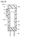
(変形例に係るリレーの構成)
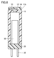
アンテナ配線13は、樹脂成形体11の面11aとは異なる面に形成されてもよい。図6~図8を参照して、樹脂成形体11の上面11bにアンテナ配線13が形成されたリレー1について説明する。図6は、リレー1の変形例を示す正面図である。図7は、リレー1の変形例を示す平面図である。図8は、図6のXI-XI線に沿った矢視断面図である。 (Configuration of relay according to modification)
Theantenna wiring 13 may be formed on a surface different from the surface 11 a of the resin molded body 11. The relay 1 in which the antenna wiring 13 is formed on the upper surface 11b of the resin molded body 11 will be described with reference to FIGS. FIG. 6 is a front view showing a modified example of the relay 1. FIG. 7 is a plan view showing a modification of the relay 1. 8 is a cross-sectional view taken along the line XI-XI in FIG.
アンテナ配線13は、樹脂成形体11の面11aとは異なる面に形成されてもよい。図6~図8を参照して、樹脂成形体11の上面11bにアンテナ配線13が形成されたリレー1について説明する。図6は、リレー1の変形例を示す正面図である。図7は、リレー1の変形例を示す平面図である。図8は、図6のXI-XI線に沿った矢視断面図である。 (Configuration of relay according to modification)
The
図6~図8に示されるように、ICチップ12は、樹脂成形体11の上面11bから露出するように、樹脂成形体11に埋設される。アンテナ配線13は、樹脂成形体11の上面11bの上に形成され、ICチップ12と接続する。絶縁膜14は、アンテナ配線13を覆うように、樹脂成形体11の上面11bの上に形成される。
6 to 8, the IC chip 12 is embedded in the resin molded body 11 so as to be exposed from the upper surface 11b of the resin molded body 11. The antenna wiring 13 is formed on the upper surface 11 b of the resin molded body 11 and is connected to the IC chip 12. The insulating film 14 is formed on the upper surface 11 b of the resin molded body 11 so as to cover the antenna wiring 13.
リレー1の変形例によれば、アンテナ配線13は、電磁石40から最も離れた位置に形成される。これにより、アンテナ配線13が送受信する電波に対する、電磁石40によって発生する磁界の影響を小さくすることができる。
According to a modification of the relay 1, the antenna wiring 13 is formed at a position farthest from the electromagnet 40. Thereby, the influence of the magnetic field generated by the electromagnet 40 on the radio wave transmitted and received by the antenna wiring 13 can be reduced.
(アンテナパターン選択装置)
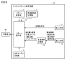
図9を参照して、樹脂成形体11に形成されるアンテナ配線のパターンを選択するアンテナパターン選択装置70について説明する。図9は、アンテナパターン選択装置70の構成を示すブロック図である。 (Antenna pattern selection device)
With reference to FIG. 9, the antennapattern selection apparatus 70 which selects the pattern of the antenna wiring formed in the resin molding 11 is demonstrated. FIG. 9 is a block diagram illustrating a configuration of the antenna pattern selection device 70.
図9を参照して、樹脂成形体11に形成されるアンテナ配線のパターンを選択するアンテナパターン選択装置70について説明する。図9は、アンテナパターン選択装置70の構成を示すブロック図である。 (Antenna pattern selection device)
With reference to FIG. 9, the antenna
アンテナパターン選択装置70は、複数のアンテナパターンから選択した1つのアンテナパターンを含む印刷プログラムを生成し、生成した印刷プログラムを印刷機60に出力する。図9に示されるように、アンテナパターン選択装置70は、第1入力部71と、第2入力部72と、通信条件設定部73と、周波数規格記憶部74と、パターン記憶部75と、対応テーブル記憶部76と、パターン選択部77とを備える。
The antenna pattern selection device 70 generates a print program including one antenna pattern selected from a plurality of antenna patterns, and outputs the generated print program to the printing press 60. As shown in FIG. 9, the antenna pattern selection device 70 includes a first input unit 71, a second input unit 72, a communication condition setting unit 73, a frequency standard storage unit 74, and a pattern storage unit 75. A table storage unit 76 and a pattern selection unit 77 are provided.
第1入力部71および第2入力部72は、ユーザからの情報の入力を受ける。第1入力部71および第2入力部72は、キーボード、マウス、タッチパネル等により構成される。
The first input unit 71 and the second input unit 72 receive input of information from the user. The first input unit 71 and the second input unit 72 are configured by a keyboard, a mouse, a touch panel, and the like.
第1入力部71は、リレー1の出荷国または出荷地域を示す出荷先情報の入力を受ける。第2入力部72は、リレー1の部品仕様、使用場所および使用状態を示す環境情報の入力を受ける。ここで、部品仕様とは、リレー1の仕様であり、仕様番号によって特定される。たとえば、ある仕様番号は、樹脂成形体11の正面側の面11aにアンテナ配線13が形成された仕様を示し、別の仕様番号は、樹脂成形体11の上面11bにアンテナ配線13が形成された仕様を示す。使用場所とは、リレー1が使用される場所(野外、工場等)である。使用状態とは、リレー1が使用されるときの状態(たとえば、周囲の電波状態等)である。
The first input unit 71 receives input of shipping destination information indicating the shipping country or shipping region of the relay 1. The second input unit 72 receives input of environmental information indicating the component specifications, use place, and use state of the relay 1. Here, the component specification is the specification of the relay 1 and is specified by the specification number. For example, a certain specification number indicates a specification in which the antenna wiring 13 is formed on the front surface 11 a of the resin molded body 11, and another specification number indicates that the antenna wiring 13 is formed on the upper surface 11 b of the resin molded body 11. The specification is shown. A use place is a place (the outdoors, a factory, etc.) where the relay 1 is used. The use state is a state when the relay 1 is used (for example, a surrounding radio wave state).
通信条件設定部73は、第2入力部72に入力された環境情報に基づいて、アンテナ配線13の形状を設定するために必要な通信条件を設定する。通信条件設定部73は、通信条件として、アンテナ配線13を印刷する場所を示す印刷スペース、アンテナ配線13に必要な通信距離、アンテナ配線13のサイズ(アンテナサイズ)などを設定する。
The communication condition setting unit 73 sets communication conditions necessary for setting the shape of the antenna wiring 13 based on the environment information input to the second input unit 72. The communication condition setting unit 73 sets, as communication conditions, a print space indicating a place where the antenna wiring 13 is printed, a communication distance necessary for the antenna wiring 13, a size of the antenna wiring 13 (antenna size), and the like.
通信条件設定部73は、第2入力部72から受けた環境情報によって示される部品仕様に従って、印刷スペースを設定する。たとえば、通信条件設定部73は、樹脂成形体11の正面側の面11aにアンテナ配線13が形成された部品仕様の仕様番号を受けた場合、面11aを印刷スペースとして設定する。
The communication condition setting unit 73 sets a print space according to the part specification indicated by the environment information received from the second input unit 72. For example, when the communication condition setting unit 73 receives the specification number of the component specification in which the antenna wiring 13 is formed on the front surface 11a of the resin molded body 11, the communication condition setting unit 73 sets the surface 11a as the print space.
通信条件設定部73は、第2入力部72から受けた環境情報によって示される使用場所に応じた通信距離を設定する。たとえば、通信条件設定部73は、使用場所が野外である場合には、使用場所が工場である場合に比べて長い通信距離を設定する。通信条件設定部73は、使用場所と通信距離とを対応付けた情報を予め記憶しており、当該情報に従って通信距離を設定する。この場合、第2入力部72は、当該情報に含まれる使用場所のみ入力を受け付けるように設定されることが好ましい。
The communication condition setting unit 73 sets a communication distance according to the place of use indicated by the environment information received from the second input unit 72. For example, when the usage location is outdoors, the communication condition setting unit 73 sets a longer communication distance than when the usage location is a factory. The communication condition setting unit 73 stores in advance information that associates the place of use with the communication distance, and sets the communication distance according to the information. In this case, it is preferable that the 2nd input part 72 is set so that only the use place contained in the said information may be received.
通信条件設定部73は、第2入力部72から受けた環境情報によって示される使用状態に従って、アンテナサイズを設定する。たとえば、通信条件設定部73は、リレー1の周囲の電波が弱いほど大きなアンテナサイズを設定する。通信条件設定部73は、使用状態(電波の強さ)とアンテナサイズとを対応付けた情報を予め記憶しており、当該情報に従ってアンテナサイズを設定する。
The communication condition setting unit 73 sets the antenna size according to the usage state indicated by the environment information received from the second input unit 72. For example, the communication condition setting unit 73 sets a larger antenna size as the radio wave around the relay 1 is weaker. The communication condition setting unit 73 stores in advance information that associates the usage state (the strength of radio waves) with the antenna size, and sets the antenna size according to the information.
また、使用状態には、上記に記載したもの以外に、リレー1の密集度が含まれてもよい。リレー1の密集度は、たとえば他のリレー1との距離、または、単位面積当たりのリレー1の設置個数により示される。複数個のリレー1が密集して使用される場合、リレー1の樹脂成形体11に印刷されたアンテナ配線13が互いに近接するため、ICチップ12による無線通信に干渉が生じることがある。この対応として、通信条件設定部73は、密集度に応じて、アンテナサイズを設定すること以外に、アンテナ配線13が形成される樹脂成形体11上の印刷スペース(樹脂成形体11の面および当該面内の位置)を設定したり、アンテナ配線の形状を通信条件の1つとして設定したりする。
In addition, the usage state may include the density of the relay 1 in addition to those described above. The density of the relays 1 is indicated by, for example, the distance from other relays 1 or the number of relays 1 installed per unit area. When a plurality of relays 1 are used densely, the antenna wiring 13 printed on the resin molded body 11 of the relay 1 is close to each other, so that interference may occur in wireless communication by the IC chip 12. As a response to this, the communication condition setting unit 73 sets the antenna size according to the density, and print space on the resin molded body 11 on which the antenna wiring 13 is formed (the surface of the resin molded body 11 and the surface Position in the plane) or the shape of the antenna wiring is set as one of the communication conditions.
周波数規格記憶部74は、国または地域ごとに設定された周波数規格を記憶する。パターン記憶部75は、予め設計された複数のアンテナパターンを記憶する。アンテナパターンとは、アンテナ配線13の形状パターンである。各アンテナパターンには、当該アンテナパターンを識別するパターン番号が付されている。パターン記憶部75が記憶する複数のアンテナパターンには、異なる形態のアンテナ(たとえば、パッチアンテナ、ループアンテナ、ダイポールアンテナなど)が含まれてもよい。
The frequency standard storage unit 74 stores a frequency standard set for each country or region. The pattern storage unit 75 stores a plurality of antenna patterns designed in advance. The antenna pattern is a shape pattern of the antenna wiring 13. Each antenna pattern is given a pattern number for identifying the antenna pattern. The plurality of antenna patterns stored in the pattern storage unit 75 may include different types of antennas (for example, patch antennas, loop antennas, dipole antennas, etc.).
対応テーブル記憶部76は、周波数規格および通信条件(印刷スペース、通信距離およびアンテナサイズなど)と、パターン番号とを対応付けた対応テーブルを記憶する。対応テーブルは、予め設定される。たとえば、ある組合せに対応するパターン番号として、当該組合せの通信距離だけ離れたリーダに対して通信可能であり、当該組合せの印刷スペースに印刷可能であり、当該組合せのアンテナサイズを満たし、かつ、当該組合せの周波数規格に含まれる周波数に共振するアンテナパターンのパターン番号が設定される。
The correspondence table storage unit 76 stores a correspondence table in which frequency standards and communication conditions (printing space, communication distance, antenna size, and the like) are associated with pattern numbers. The correspondence table is set in advance. For example, as a pattern number corresponding to a certain combination, communication is possible with respect to a reader separated by the communication distance of the combination, printing is possible in the printing space of the combination, the antenna size of the combination is satisfied, and A pattern number of an antenna pattern that resonates at a frequency included in the frequency standard of the combination is set.
パターン選択部77は、第1入力部71から受けた出荷先情報と、通信条件設定部73から受けた通信条件情報とに基づいて、複数のアンテナパターンから1つのアンテナパターンを選択する。パターン選択部77は、選択したアンテナパターンをパターン記憶部75から読み出し、当該アンテナパターンを含む印刷プログラムを生成する。パターン選択部77は、生成した印刷プログラムを印刷機60に出力する。
The pattern selection unit 77 selects one antenna pattern from a plurality of antenna patterns based on the shipping destination information received from the first input unit 71 and the communication condition information received from the communication condition setting unit 73. The pattern selection unit 77 reads the selected antenna pattern from the pattern storage unit 75 and generates a print program including the antenna pattern. The pattern selection unit 77 outputs the generated printing program to the printing machine 60.
パターン選択部77は、出荷先情報によって示される出荷国または出荷地域に対応する周波数規格を周波数規格記憶部74から読み出す。パターン選択部77は、読み出した周波数規格と、通信条件設定部73から受けた通信条件情報(印刷スペース、通信距離およびアンテナサイズなど)とに対応するアンテナ番号を対応テーブル記憶部76から特定する。パターン選択部77は、特定したアンテナ番号のアンテナパターンを、印刷プログラムに含ませるアンテナパターンとしてパターン記憶部75から読み出す。
The pattern selection unit 77 reads the frequency standard corresponding to the shipping country or the shipping region indicated by the shipping destination information from the frequency standard storage unit 74. The pattern selection unit 77 specifies the antenna number corresponding to the read frequency standard and the communication condition information (print space, communication distance, antenna size, etc.) received from the communication condition setting unit 73 from the correspondence table storage unit 76. The pattern selection unit 77 reads the antenna pattern of the identified antenna number from the pattern storage unit 75 as an antenna pattern to be included in the print program.
なお、パターン選択部77は、アンテナパターンのうちICチップ12の端子に接続する基準点を指定した印刷プログラムを出力する。印刷機60は、搬送された半製品15(図4の(c)参照)を撮像することにより得られた画像からICチップ12の位置を特定し、当該ICチップ12の位置と基準点との位置合わせを行なったうえで、指定されたアンテナパターンのアンテナ配線13を印刷する。
Note that the pattern selection unit 77 outputs a printing program that specifies a reference point to be connected to the terminal of the IC chip 12 in the antenna pattern. The printing press 60 identifies the position of the IC chip 12 from an image obtained by imaging the conveyed semi-finished product 15 (see FIG. 4C), and determines the position of the IC chip 12 and the reference point. After alignment, the antenna wiring 13 having the designated antenna pattern is printed.
アンテナパターン選択装置70のハードウェアは、ユーザーインターフェースと、OS(Operating System)を含む各種プログラムを実行するCPU(Central Processing Unit)と、各種データを格納するROM(Read Only Memory)と、CPUでのプログラムの実行に必要なデータを格納するための作業領域を提供するRAMと、CPUで実行されるプログラムなどを不揮発的に格納するハードディスク(HDD)とによって構成される。上記の第1入力部71および第2入力部72は、ユーザーインターフェースによって構成される。通信条件設定部73およびパターン選択部77は、HDDに格納されたプログラムをCPUが実行することにより実現される。周波数規格記憶部74、パターン記憶部75および対応テーブル記憶部76は、ROMおよびRAMによって構成される。
The hardware of the antenna pattern selection device 70 includes a user interface, a CPU (Central Processing Unit) that executes various programs including an OS (Operating System), a ROM (Read Only Memory) that stores various data, and a CPU. It is composed of a RAM that provides a work area for storing data necessary for program execution, and a hard disk (HDD) that stores programs executed by the CPU in a nonvolatile manner. The first input unit 71 and the second input unit 72 are configured by a user interface. The communication condition setting unit 73 and the pattern selection unit 77 are realized by the CPU executing a program stored in the HDD. The frequency standard storage unit 74, the pattern storage unit 75, and the correspondence table storage unit 76 are configured by a ROM and a RAM.
(利点)
以上のように、リレー1の製造方法は、ICチップ12を囲むように樹脂を射出することにより、ICチップ12を埋設した樹脂成形体11を成形する樹脂成形工程(第1工程)と、樹脂成形体11をリレー1の外装部品10として、リレー1の本体であるベース部材20に取り付ける組立工程(第2工程)と、樹脂成形体11の面11a上に、ICチップ12が無線通信するためのアンテナ配線13を印刷するアンテナ配線形成工程(第3工程)とを備える。 (advantage)
As described above, the method for manufacturing therelay 1 includes a resin molding step (first step) for molding the resin molded body 11 in which the IC chip 12 is embedded by injecting resin so as to surround the IC chip 12, and the resin. An assembly process (second process) in which the molded body 11 is used as the exterior part 10 of the relay 1 and attached to the base member 20 that is the main body of the relay 1, and the IC chip 12 communicates wirelessly on the surface 11 a of the resin molded body 11. An antenna wiring forming step (third step) for printing the antenna wiring 13 of the antenna.
以上のように、リレー1の製造方法は、ICチップ12を囲むように樹脂を射出することにより、ICチップ12を埋設した樹脂成形体11を成形する樹脂成形工程(第1工程)と、樹脂成形体11をリレー1の外装部品10として、リレー1の本体であるベース部材20に取り付ける組立工程(第2工程)と、樹脂成形体11の面11a上に、ICチップ12が無線通信するためのアンテナ配線13を印刷するアンテナ配線形成工程(第3工程)とを備える。 (advantage)
As described above, the method for manufacturing the
上記の構成によれは、樹脂成形体11を外装部品10の一部としてベース部材20に取り付けた後にアンテナ配線13が印刷される。そのため、アンテナ配線13が形成されていない半製品15の状態で在庫しておき、出荷する直前にアンテナ配線13を形成して、アンテナ配線13とICチップ12とでICタグを構成させることができる。たとえば、アンテナ配線13は、出荷先が決定した後に、出荷先の周波数規格等に応じた形状を有するように形成される。このように、アンテナの共振周波数またはアンテナ形態が互いに異なる多種類のアンテナパターンから選択された1つのアンテナパターンを有するICタグを備えたリレー1を、受注してから短時間で容易に製造することができる。
According to the above configuration, the antenna wiring 13 is printed after the resin molded body 11 is attached to the base member 20 as a part of the exterior component 10. Therefore, it can be stocked in the state of the semi-finished product 15 in which the antenna wiring 13 is not formed, the antenna wiring 13 can be formed immediately before shipping, and the IC tag can be configured by the antenna wiring 13 and the IC chip 12. . For example, the antenna wiring 13 is formed so as to have a shape according to the frequency standard of the shipping destination after the shipping destination is determined. Thus, the relay 1 including an IC tag having one antenna pattern selected from a plurality of types of antenna patterns having different antenna resonance frequencies or antenna forms can be easily manufactured in a short time after receiving an order. Can do.
本実施の形態1の製造方法は、リレー1の出荷先の周波数規格およびリレー1の使用環境の少なくとも一方に応じて、アンテナ配線13のパターンを決定するアンテナパターン決定工程(第4工程)をさらに備える。アンテナ配線形成工程において、アンテナパターン決定工程によって決定されたパターンのアンテナ配線13が印刷される。これにより、出荷先の周波数規格およびリレー1の使用環境の少なくとも一方に応じたアンテナ配線13を備えるリレー1を容易に製造することができる。
The manufacturing method according to the first embodiment further includes an antenna pattern determination step (fourth step) for determining the pattern of the antenna wiring 13 according to at least one of the frequency standard of the shipping destination of the relay 1 and the use environment of the relay 1. Prepare. In the antenna wiring formation process, the antenna wiring 13 having the pattern determined in the antenna pattern determination process is printed. Thereby, the relay 1 provided with the antenna wiring 13 according to at least one of the shipping destination frequency standard and the usage environment of the relay 1 can be easily manufactured.
リレー(製品)1の外装部品10は、樹脂成形体11を備える。樹脂成形体11の表面は、外装部品10の外表面となる面(第1面)11aを含む。さらに、外装部品10は、樹脂成形体11に埋設され、リレー1を識別する識別データを記憶するICチップ12と、面11aの上に形成された、ICチップ12が無線通信するためのアンテナ配線13とを備える。
The exterior part 10 of the relay (product) 1 includes a resin molded body 11. The surface of the resin molded body 11 includes a surface (first surface) 11 a that is an outer surface of the exterior component 10. Further, the exterior component 10 is embedded in the resin molded body 11, and an IC chip 12 that stores identification data for identifying the relay 1 and antenna wiring formed on the surface 11a for wireless communication with the IC chip 12 13.
上記の構成によれば、アンテナ配線13は、外装部品10の外表面である面11aに形成される。そのため、アンテナ配線13が形成されていない半製品15の状態で在庫しておき、出荷する直前にアンテナ配線13を形成して、アンテナ配線13とICチップ12とでICタグを構成させることができる。たとえば、アンテナ配線13は、出荷先が決定した後に、出荷先の周波数規格等に応じた形状を有するように形成される。このように、リレー1の外装部品10は、アンテナの共振周波数またはアンテナ形態が互いに異なる多種類のアンテナパターンから選択された1つのアンテナパターンを有するICタグを備える。これにより、多種類のアンテナパターンから選択された1つのアンテナパターンを有するICタグを備えたリレー1を、受注してから短時間で容易に製造することができる。
According to the above configuration, the antenna wiring 13 is formed on the surface 11a which is the outer surface of the exterior component 10. Therefore, it can be stocked in the state of the semi-finished product 15 in which the antenna wiring 13 is not formed, the antenna wiring 13 can be formed immediately before shipping, and the IC tag can be configured by the antenna wiring 13 and the IC chip 12. . For example, the antenna wiring 13 is formed so as to have a shape according to the frequency standard of the shipping destination after the shipping destination is determined. As described above, the exterior component 10 of the relay 1 includes an IC tag having one antenna pattern selected from many types of antenna patterns having different antenna resonance frequencies or antenna forms. Thereby, the relay 1 provided with the IC tag having one antenna pattern selected from the various types of antenna patterns can be easily manufactured in a short time after receiving an order.
従来のように、接着剤等によりICタグが製品に貼付される場合、ICタグが製品から容易に剥がすことができる。そのため、不正な製品に正当なICタグを貼付したり、正当な製品に不正なICタグを貼付したりといった不正行為が容易であった。しかしながら、本実施の形態1に係る外装部品10では、ICチップ12が外装部品10の本体となる樹脂成形体11に埋設されるため、ICチップ12を不正に取り換えるためには、外装部品10ごと取り換える必要がある。そのため、上記のような不正行為を抑制することができる。
As before, when an IC tag is affixed to a product with an adhesive or the like, the IC tag can be easily peeled off from the product. For this reason, it is easy to perform an illegal act such as attaching a legitimate IC tag to an unauthorized product or attaching an unauthorized IC tag to an authorized product. However, in the exterior component 10 according to the first embodiment, since the IC chip 12 is embedded in the resin molded body 11 that is the main body of the exterior component 10, in order to replace the IC chip 12 illegally, the exterior component 10 It needs to be replaced. Therefore, it is possible to suppress the illegal acts as described above.
外装部品10は、アンテナ配線13の上に形成された絶縁膜14をさらに備えることが好ましい。これにより、アンテナ配線13の硫化、酸化または機械的負荷による摩耗を防ぐことができる。
The exterior component 10 preferably further includes an insulating film 14 formed on the antenna wiring 13. As a result, it is possible to prevent wear of the antenna wiring 13 due to sulfurization, oxidation, or mechanical load.
ICチップ12は、面11aから露出する。アンテナ配線13は、ICチップ12に電気的に接続される。これにより、アンテナ配線13をICチップ12に直接接続されたアンテナとして使用することができる。
The IC chip 12 is exposed from the surface 11a. The antenna wiring 13 is electrically connected to the IC chip 12. Thereby, the antenna wiring 13 can be used as an antenna directly connected to the IC chip 12.
本実施の形態1に係るアンテナパターン選択装置70は、第1入力部71と、第2入力部72と、通信条件設定部73と、パターン選択部77とを備える。第1入力部71は、リレー1の出荷先を示す出荷先情報の入力を受ける。第2入力部72は、リレー1の使用環境を示す環境情報の入力を受ける。通信条件設定部73は、環境情報によって示される使用環境に基づいて、アンテナ配線13の通信条件を設定する。パターン選択部77は、出荷先および通信条件とアンテナ配線13のパターンとを対応付けた対応テーブルに基づいて、出荷先情報によって示される出荷先と、通信条件設定部73によって設定された通信条件に対応するアンテナ配線13のパターンを選択する。これにより、出荷先の周波数規格および使用環境に応じたアンテナ配線13のパターンを容易に選択することができる。
The antenna pattern selection device 70 according to the first embodiment includes a first input unit 71, a second input unit 72, a communication condition setting unit 73, and a pattern selection unit 77. The first input unit 71 receives input of shipping destination information indicating the shipping destination of the relay 1. The second input unit 72 receives input of environment information indicating the use environment of the relay 1. The communication condition setting unit 73 sets the communication condition of the antenna wiring 13 based on the use environment indicated by the environment information. The pattern selection unit 77 sets the shipping destination indicated by the shipping destination information and the communication condition set by the communication condition setting unit 73 based on the correspondence table in which the shipping destination and communication conditions are associated with the pattern of the antenna wiring 13. The corresponding antenna wiring 13 pattern is selected. Thereby, the pattern of the antenna wiring 13 according to the frequency standard of a shipping destination and use environment can be selected easily.
<実施の形態2>
上記の実施の形態1では、ICチップ12に直接接続するアンテナとしてアンテナ配線13を使用する。これに対し、本実施の形態2では、ICチップ12を含むICモジュールから発信する微弱電波を増幅するブースターアンテナとしてアンテナ配線13が使用される。そのため、アンテナ配線13は、ICチップ12に電気的に直接接続しない。 <Embodiment 2>
In the first embodiment, theantenna wiring 13 is used as an antenna that is directly connected to the IC chip 12. On the other hand, in the second embodiment, the antenna wiring 13 is used as a booster antenna that amplifies weak radio waves transmitted from the IC module including the IC chip 12. Therefore, the antenna wiring 13 is not electrically connected directly to the IC chip 12.
上記の実施の形態1では、ICチップ12に直接接続するアンテナとしてアンテナ配線13を使用する。これに対し、本実施の形態2では、ICチップ12を含むICモジュールから発信する微弱電波を増幅するブースターアンテナとしてアンテナ配線13が使用される。そのため、アンテナ配線13は、ICチップ12に電気的に直接接続しない。 <Embodiment 2>
In the first embodiment, the
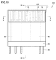
図10~図13を参照して、実施の形態2に係る外装部品110を備えたリレー(製品)101の概略的な構成について説明する。図10は、実施の形態2に係るリレー101を示す正面図である。図11は、図10のX-X線に沿った矢視断面図である。図12は、図10のXI-XI線に沿った矢視断面図である。図13は、ICモジュール16の概略的な構成を示す図である。
A schematic configuration of a relay (product) 101 including the exterior part 110 according to the second embodiment will be described with reference to FIGS. FIG. 10 is a front view showing the relay 101 according to the second embodiment. 11 is a cross-sectional view taken along line XX in FIG. 12 is a cross-sectional view taken along line XI-XI in FIG. FIG. 13 is a diagram showing a schematic configuration of the IC module 16.
図10~図12に示されるように、リレー101は、外装部品10の代わりに外装部品110を備える点で実施の形態1のリレー1と相違する。外装部品110は、ICチップ12の代わりにICモジュール16を備える点で外装部品10と相違する。これ以外の点は、実施の形態1のリレー1と同じであるので、以下ではそれらの説明については繰り返さない。
As shown in FIG. 10 to FIG. 12, the relay 101 is different from the relay 1 of the first embodiment in that it includes an exterior component 110 instead of the exterior component 10. The exterior component 110 is different from the exterior component 10 in that an IC module 16 is provided instead of the IC chip 12. Since points other than this are the same as those of relay 1 of the first embodiment, description thereof will not be repeated below.
図13に示されるように、ICモジュール16は、ICチップ12と、ICチップ12に電気的に直接接続されたIC側アンテナ17とを含む。ICチップ12は、IC側アンテナ17を介して無線通信を行なう。IC側アンテナ17は、比較的小さいサイズのアンテナであり、微弱電波しか送信できない。そのため、本実施の形態2では、IC側アンテナ17から発信する微弱電波を増幅するブースターアンテナとしてアンテナ配線13を機能させる。
As shown in FIG. 13, the IC module 16 includes an IC chip 12 and an IC-side antenna 17 that is electrically connected directly to the IC chip 12. The IC chip 12 performs wireless communication via the IC side antenna 17. The IC side antenna 17 is an antenna having a relatively small size and can transmit only weak radio waves. Therefore, in the second embodiment, the antenna wiring 13 is caused to function as a booster antenna that amplifies weak radio waves transmitted from the IC-side antenna 17.
図10~図12に戻って、ICモジュール16は、樹脂成形体11における面11aの裏側の面11cから露出するように、樹脂成形体11に埋設される。アンテナ配線13は、面11aにおけるICモジュール16に対向する位置に形成され、ICモジュール16のIC側アンテナ17と電磁結合する。すなわち、アンテナ配線13は、ICモジュール16のIC側アンテナ17とインピーダンスマッチングする。これにより、ICチップ12は、IC側アンテナ17およびアンテナ配線13を介して無線通信できる。
10 to 12, the IC module 16 is embedded in the resin molded body 11 so as to be exposed from the surface 11c on the back side of the surface 11a of the resin molded body 11. The antenna wiring 13 is formed at a position facing the IC module 16 on the surface 11 a and is electromagnetically coupled to the IC-side antenna 17 of the IC module 16. That is, the antenna wiring 13 is impedance-matched with the IC-side antenna 17 of the IC module 16. Accordingly, the IC chip 12 can perform wireless communication via the IC-side antenna 17 and the antenna wiring 13.
このように、本実施の形態2の外装部品110によれば、ICモジュール16は、樹脂成形体11における面(第1面)11aの裏側の面(第2面)11cから露出するように、樹脂成形体11に埋設される。アンテナ配線13は、ICモジュール16に対向するように面11aの上に形成される。これにより、リレー101の外部からの機械的負荷、湿気等の環境負荷に起因したICモジュール16の故障を抑制することができる。
As described above, according to the exterior component 110 of the second embodiment, the IC module 16 is exposed from the surface (second surface) 11c on the back side of the surface (first surface) 11a of the resin molded body 11. It is embedded in the resin molded body 11. The antenna wiring 13 is formed on the surface 11 a so as to face the IC module 16. Thereby, failure of the IC module 16 due to an environmental load such as a mechanical load and moisture from the outside of the relay 101 can be suppressed.
アンテナ配線13は、ICモジュール16のIC側アンテナ17と電磁結合可能な位置に形成される。そのため、印刷機60は、ICモジュール16の位置を特定し、当該位置に基づいてアンテナ配線13を印刷する必要がある。樹脂成形体11の内表面側に埋設されたICモジュール16の位置の特定を容易にするために、樹脂成形体11を透明材料で成形することが好ましい。
The antenna wiring 13 is formed at a position where it can be electromagnetically coupled to the IC side antenna 17 of the IC module 16. Therefore, the printing machine 60 needs to specify the position of the IC module 16 and print the antenna wiring 13 based on the position. In order to easily specify the position of the IC module 16 embedded on the inner surface side of the resin molded body 11, it is preferable to mold the resin molded body 11 with a transparent material.
<実施の形態3>
上記の実施の形態2では、アンテナ配線13をICモジュール16と対向する位置に形成した。これに対し、本実施の形態3では、外装部品の外表面に露出するようにICモジュール16を配置し、ICモジュール16と重ならないようにアンテナ配線13を形成する。 <Embodiment 3>
In the second embodiment, theantenna wiring 13 is formed at a position facing the IC module 16. In contrast, in the third embodiment, the IC module 16 is disposed so as to be exposed on the outer surface of the exterior component, and the antenna wiring 13 is formed so as not to overlap the IC module 16.
上記の実施の形態2では、アンテナ配線13をICモジュール16と対向する位置に形成した。これに対し、本実施の形態3では、外装部品の外表面に露出するようにICモジュール16を配置し、ICモジュール16と重ならないようにアンテナ配線13を形成する。 <Embodiment 3>
In the second embodiment, the
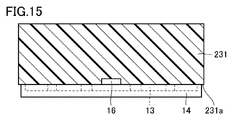
図14~図16を参照して、実施の形態3に係る外装部品210を備えたリレー(製品)201の概略的な構成について説明する。図14は、実施の形態3に係るリレー201を示す正面図である。図15は、図14のX-X線に沿った矢視断面図である。図16は、図14のXI-XI線に沿った矢視断面図である。
A schematic configuration of a relay (product) 201 including the exterior component 210 according to the third embodiment will be described with reference to FIGS. FIG. 14 is a front view showing the relay 201 according to the third embodiment. 15 is a cross-sectional view taken along the line XX in FIG. 16 is a cross-sectional view taken along line XI-XI in FIG.
図14~図16に示されるように、リレー201は、外装部品110の代わりに外装部品210を備える点で実施の形態2のリレー101と相違する。外装部品210は、樹脂成形体11の代わりに樹脂成形体211を備える点で外装部品110と相違する。これ以外の点は、実施の形態2のリレー101と同じであるので、以下ではそれらの説明については繰り返さない。
As shown in FIGS. 14 to 16, the relay 201 is different from the relay 101 of the second embodiment in that it includes an exterior component 210 instead of the exterior component 110. The exterior component 210 is different from the exterior component 110 in that a resin molded body 211 is provided instead of the resin molded body 11. Since points other than this are the same as those of relay 101 of the second embodiment, description thereof will not be repeated below.
樹脂成形体211は、第1樹脂成形部品221と第2樹脂成形部品231とを含む。第1樹脂成形部品221と第2樹脂成形部品231とは、接着剤または機械的な接合構造により一体化され、樹脂成形体211を構成する。これにより、外装部品210を大型化できる。さらに、複雑な形状の外装部品210を容易に実現することができる。
The resin molded body 211 includes a first resin molded part 221 and a second resin molded part 231. The first resin molded part 221 and the second resin molded part 231 are integrated by an adhesive or a mechanical joining structure to constitute a resin molded body 211. Thereby, the exterior component 210 can be enlarged. Furthermore, the exterior component 210 having a complicated shape can be easily realized.
第1樹脂成形部品221は筒状である。第1樹脂成形部品221における一方の開口端は、ベース部材20における電磁石40および接点部50が実装された面に接合する。
The first resin molded part 221 is cylindrical. One open end of the first resin molded component 221 is joined to the surface of the base member 20 on which the electromagnet 40 and the contact portion 50 are mounted.
第2樹脂成形部品231は、板状であり、第1樹脂成形部品221における他方の開口端を閉じるように当該他方の開口端に接合する。
The second resin molded part 231 has a plate shape and is joined to the other open end so as to close the other open end of the first resin molded part 221.
第1樹脂成形部品221の正面側の面221aと、第2樹脂成形部品231の正面側の面231aとは、同一平面上にある。
The front surface 221a of the first resin molded part 221 and the front surface 231a of the second resin molded part 231 are on the same plane.
ICモジュール16は、面231aから露出するように第2樹脂成形部品231に埋設される。アンテナ配線13は、第1樹脂成形部品221の面221aにおける、ICモジュール16のIC側アンテナ17(図13参照)と電磁結合する位置に形成される。
The IC module 16 is embedded in the second resin molded part 231 so as to be exposed from the surface 231a. The antenna wiring 13 is formed on the surface 221a of the first resin molded part 221 at a position where it is electromagnetically coupled to the IC side antenna 17 (see FIG. 13) of the IC module 16.
このように、樹脂成形体211は、第1樹脂成形部品221と第2樹脂成形部品231とを含む。アンテナ配線13は、第1樹脂成形部品221の外表面の一部である面(第1面)221aの上に形成される。第2樹脂成形部品の外表面は、面221aと同一平面上にある面(第2面)231aを含む。ICモジュール16は、第2樹脂成形部品231に埋設され、面231aから露出する。これにより、第1樹脂成形部品221と第2樹脂成形部品231との境界部分に、アンテナ配線13が形成されない。その結果、アンテナ配線13の断線を防止することができる。
Thus, the resin molded body 211 includes the first resin molded part 221 and the second resin molded part 231. The antenna wiring 13 is formed on a surface (first surface) 221 a that is a part of the outer surface of the first resin molded part 221. The outer surface of the second resin molded part includes a surface (second surface) 231a that is on the same plane as the surface 221a. The IC module 16 is embedded in the second resin molded part 231 and exposed from the surface 231a. As a result, the antenna wiring 13 is not formed at the boundary between the first resin molded part 221 and the second resin molded part 231. As a result, disconnection of the antenna wiring 13 can be prevented.
今回開示された実施の形態はすべての点で例示であって制限的なものではないと考えられるべきである。本発明の範囲は、上記した説明ではなく、請求の範囲によって示され、請求の範囲と均等の意味および範囲内でのすべての変更が含まれることが意図される。
The embodiment disclosed this time should be considered as illustrative in all points and not restrictive. The scope of the present invention is defined by the terms of the claims, rather than the description above, and is intended to include any modifications within the scope and meaning equivalent to the terms of the claims.
1,101,201 リレー、10,110,210 外装部品、11,211 樹脂成形体、11a,11c,221a,231a 面、11b 上面、12 ICチップ、13 アンテナ配線、14 絶縁膜、15 半製品、16 ICモジュール、17 IC側アンテナ、20 ベース部材、30 端子、40 電磁石、50 接点部、60 印刷機、70 アンテナパターン選択装置、71 第1入力部、72 第2入力部、73 通信条件設定部、74 周波数規格記憶部、75 パターン記憶部、76 対応テーブル記憶部、77 パターン選択部、100 仮固定シート、221 第1樹脂成形部品、231 第2樹脂成形部品。
1, 101, 201 relay, 10, 110, 210 exterior parts, 11, 211 resin molded body, 11a, 11c, 221a, 231a surface, 11b upper surface, 12 IC chip, 13 antenna wiring, 14 insulating film, 15 semi-finished product, 16 IC module, 17 IC side antenna, 20 base member, 30 terminal, 40 electromagnet, 50 contact part, 60 printing machine, 70 antenna pattern selection device, 71 first input part, 72 second input part, 73 communication condition setting part 74 frequency standard storage unit, 75 pattern storage unit, 76 correspondence table storage unit, 77 pattern selection unit, 100 temporary fixing sheet, 221 first resin molded part, 231 second resin molded part.
Claims (9)
- 製品の製造方法であって、
前記製品を識別するための識別データを記憶するICチップを囲むように樹脂を射出することにより、前記ICチップを埋設した樹脂成形体を成形する第1工程と、
前記樹脂成形体を前記製品の外装部品として、製品本体に取り付ける第2工程と、
前記製品本体に取り付けられた前記樹脂成形体の外表面上に、前記ICチップが無線通信するためのアンテナ配線を印刷する第3工程とを備える、製品の製造方法。 A method for manufacturing a product, comprising:
A first step of molding a resin molded body in which the IC chip is embedded by injecting resin so as to surround an IC chip storing identification data for identifying the product;
A second step of attaching the resin molded body to the product body as an exterior part of the product;
And a third step of printing antenna wiring for wireless communication of the IC chip on the outer surface of the resin molded body attached to the product main body. - 前記製品の出荷先の周波数規格および前記製品の使用環境の少なくとも一方に応じて、前記アンテナ配線のパターンを決定する第4工程をさらに備え、
前記第3工程において、前記第4工程によって決定されたパターンの前記アンテナ配線を印刷する、請求項1に記載の製品の製造方法。 A fourth step of determining a pattern of the antenna wiring according to at least one of a frequency standard of a shipping destination of the product and a use environment of the product;
The method for manufacturing a product according to claim 1, wherein in the third step, the antenna wiring having a pattern determined in the fourth step is printed. - 製品の外装部品であって、
樹脂成形体を備え、前記樹脂成形体の表面は、前記外装部品の外表面となる第1面を含み、
前記外装部品は、
前記樹脂成形体に埋設され、前記製品を識別する識別データを記憶するICチップと、
前記第1面の上に形成された、前記ICチップが無線通信するためのアンテナ配線とをさらに備える、外装部品。 Product exterior parts,
Comprising a resin molded body, the surface of the resin molded body includes a first surface serving as an outer surface of the exterior component;
The exterior part is
An IC chip embedded in the resin molding and storing identification data for identifying the product;
An exterior part further comprising antenna wiring formed on the first surface for wireless communication of the IC chip. - 前記アンテナ配線の上に形成された絶縁膜をさらに備える、請求項3に記載の外装部品。 The exterior component according to claim 3, further comprising an insulating film formed on the antenna wiring.
- 前記ICチップは、前記第1面から露出し、
前記アンテナ配線は、前記ICチップに電気的に接続される、請求項3または4に記載の外装部品。 The IC chip is exposed from the first surface,
The exterior component according to claim 3 or 4, wherein the antenna wiring is electrically connected to the IC chip. - 前記ICチップに接続されたIC側アンテナをさらに備え、
前記ICチップと前記IC側アンテナとは、一体化されてICモジュールを構成し、
前記樹脂成形体は、前記ICモジュールを埋設し、
前記アンテナ配線は、前記IC側アンテナと電磁結合するブースターアンテナである、請求項3または4に記載の外装部品。 An IC-side antenna connected to the IC chip;
The IC chip and the IC-side antenna are integrated to form an IC module,
The resin molded body embeds the IC module,
The exterior component according to claim 3 or 4, wherein the antenna wiring is a booster antenna that electromagnetically couples with the IC-side antenna. - 前記樹脂成形体の表面は、前記外装部品の内表面となる第2面を含み、
前記第2面は、前記第1面の裏側の面であり、
前記ICモジュールは、前記第2面から露出するように前記樹脂成形体に埋設され、
前記アンテナ配線は、前記ICモジュールに対向するように前記第1面の上に形成される、請求項6に記載の外装部品。 The surface of the resin molded body includes a second surface serving as an inner surface of the exterior part,
The second surface is a surface on the back side of the first surface,
The IC module is embedded in the resin molded body so as to be exposed from the second surface,
The exterior component according to claim 6, wherein the antenna wiring is formed on the first surface so as to face the IC module. - 前記樹脂成形体は、第1樹脂成形部品と第2樹脂成形部品とを含み、
前記第1面は、前記第1樹脂成形部品の外表面の一部であり、
前記第2樹脂成形部品の外表面は、前記第1面と同一平面上にある第2面を含み、
前記ICモジュールは、前記第2樹脂成形部品に埋設され、前記第2面から露出する、請求項6に記載の外装部品。 The resin molded body includes a first resin molded part and a second resin molded part,
The first surface is a part of the outer surface of the first resin molded part,
The outer surface of the second resin molded part includes a second surface that is coplanar with the first surface,
The exterior component according to claim 6, wherein the IC module is embedded in the second resin molded component and exposed from the second surface. - 請求項3から8のいずれか1項に記載の外装部品における前記アンテナ配線のパターンを選択するアンテナパターン選択装置であって、
前記製品の出荷先を示す出荷先情報の入力を受ける第1入力部と、
前記製品の使用環境を示す環境情報の入力を受ける第2入力部と、
前記環境情報によって示される使用環境に基づいて、前記アンテナ配線の通信条件を設定する通信条件設定部と、
出荷先および通信条件と前記アンテナ配線のパターンとを対応付けた情報に基づいて、前記出荷先情報によって示される出荷先と、前記通信条件設定部によって設定された通信条件に対応する前記アンテナ配線のパターンを選択するパターン選択部とを備える、アンテナパターン選択装置。 An antenna pattern selection device for selecting a pattern of the antenna wiring in the exterior part according to any one of claims 3 to 8,
A first input unit for receiving shipping destination information indicating a shipping destination of the product;
A second input unit for receiving input of environmental information indicating a use environment of the product;
A communication condition setting unit for setting a communication condition of the antenna wiring based on a use environment indicated by the environment information;
Based on the information associating the shipping destination and communication condition with the antenna wiring pattern, the shipping destination indicated by the shipping destination information and the antenna wiring corresponding to the communication condition set by the communication condition setting unit An antenna pattern selection device comprising: a pattern selection unit that selects a pattern.
Priority Applications (3)
| Application Number | Priority Date | Filing Date | Title |
|---|---|---|---|
| CN201780071288.3A CN109997153A (en) | 2017-02-22 | 2017-11-16 | Manufacturing method, exterior member and the antenna pattern selection device of product |
| US16/462,277 US11322828B2 (en) | 2017-02-22 | 2017-11-16 | Method of manufacturing product, exterior jacket component and antenna pattern selection device |
| EP17898167.6A EP3588384B1 (en) | 2017-02-22 | 2017-11-16 | Method for manufacturing product, exterior component, and device for selecting antenna pattern |
Applications Claiming Priority (2)
| Application Number | Priority Date | Filing Date | Title |
|---|---|---|---|
| JP2017-030838 | 2017-02-22 | ||
| JP2017030838A JP6658607B2 (en) | 2017-02-22 | 2017-02-22 | Product manufacturing method, exterior parts and antenna pattern selection device |
Publications (1)
| Publication Number | Publication Date |
|---|---|
| WO2018154880A1 true WO2018154880A1 (en) | 2018-08-30 |
Family
ID=63254193
Family Applications (1)
| Application Number | Title | Priority Date | Filing Date |
|---|---|---|---|
| PCT/JP2017/041271 WO2018154880A1 (en) | 2017-02-22 | 2017-11-16 | Method for manufacturing product, exterior component, and device for selecting antenna pattern |
Country Status (6)
| Country | Link |
|---|---|
| US (1) | US11322828B2 (en) |
| EP (1) | EP3588384B1 (en) |
| JP (1) | JP6658607B2 (en) |
| CN (1) | CN109997153A (en) |
| TW (1) | TW201832413A (en) |
| WO (1) | WO2018154880A1 (en) |
Families Citing this family (1)
| Publication number | Priority date | Publication date | Assignee | Title |
|---|---|---|---|---|
| WO2023139864A1 (en) * | 2022-01-24 | 2023-07-27 | サトーホールディングス株式会社 | Formed body and method for producing formed body |
Citations (6)
| Publication number | Priority date | Publication date | Assignee | Title |
|---|---|---|---|---|
| JP2000294577A (en) | 1999-04-06 | 2000-10-20 | Sony Chem Corp | Semiconductor device |
| JP2002261421A (en) | 2001-03-06 | 2002-09-13 | Matsushita Electric Ind Co Ltd | Method of manufacturing component mounted with electronic component, method of manufacturing finished product mounted with electronic component and finished product mounted with semiconductor component |
| JP2005301443A (en) | 2004-04-07 | 2005-10-27 | Bridgestone Corp | Rfid tag and circuit constant adjusting method for rfid tag |
| JP2006039902A (en) * | 2004-07-27 | 2006-02-09 | Ntn Corp | Uhf band radio ic tag |
| JP2007096768A (en) | 2005-09-29 | 2007-04-12 | Omron Corp | Antenna unit and non-contact ic tag |
| JP2008210344A (en) | 2007-02-28 | 2008-09-11 | Omron Corp | Ic tag and manufacturing method therefor |
Family Cites Families (10)
| Publication number | Priority date | Publication date | Assignee | Title |
|---|---|---|---|---|
| JP4089167B2 (en) | 2001-03-30 | 2008-05-28 | 三菱マテリアル株式会社 | RFID tag |
| JP4052111B2 (en) * | 2002-06-07 | 2008-02-27 | ソニー株式会社 | Wireless information storage medium |
| JP4290620B2 (en) * | 2004-08-31 | 2009-07-08 | 富士通株式会社 | RFID tag, RFID tag antenna, RFID tag antenna sheet, and RFID tag manufacturing method |
| WO2006059731A1 (en) * | 2004-12-03 | 2006-06-08 | Hallys Corporation | Electronic component production method and electronic component production equipment |
| JP4796628B2 (en) * | 2006-06-02 | 2011-10-19 | 株式会社日立製作所 | IC tag inlet manufacturing method |
| CN101587845A (en) * | 2008-05-21 | 2009-11-25 | 资茂科技股份有限公司 | Packaging method and packaging structure of electronic volume label and personnel management-control method in dust free room |
| EP2776982A4 (en) | 2011-11-07 | 2015-08-05 | Tego Inc | Rfid drive management facility |
| US9286564B2 (en) * | 2012-11-20 | 2016-03-15 | Xerox Corporation | Apparatuses and methods for printed radio frequency identification (RFID) tags |
| DE102014119663A1 (en) * | 2014-12-29 | 2016-06-30 | Infineon Technologies Ag | smart card |
| US11239179B2 (en) * | 2018-11-28 | 2022-02-01 | Shiann-Tsong Tsai | Semiconductor package and fabrication method thereof |
-
2017
- 2017-02-22 JP JP2017030838A patent/JP6658607B2/en not_active Expired - Fee Related
- 2017-11-16 CN CN201780071288.3A patent/CN109997153A/en active Pending
- 2017-11-16 EP EP17898167.6A patent/EP3588384B1/en active Active
- 2017-11-16 US US16/462,277 patent/US11322828B2/en active Active
- 2017-11-16 WO PCT/JP2017/041271 patent/WO2018154880A1/en unknown
- 2017-11-27 TW TW106141173A patent/TW201832413A/en unknown
Patent Citations (6)
| Publication number | Priority date | Publication date | Assignee | Title |
|---|---|---|---|---|
| JP2000294577A (en) | 1999-04-06 | 2000-10-20 | Sony Chem Corp | Semiconductor device |
| JP2002261421A (en) | 2001-03-06 | 2002-09-13 | Matsushita Electric Ind Co Ltd | Method of manufacturing component mounted with electronic component, method of manufacturing finished product mounted with electronic component and finished product mounted with semiconductor component |
| JP2005301443A (en) | 2004-04-07 | 2005-10-27 | Bridgestone Corp | Rfid tag and circuit constant adjusting method for rfid tag |
| JP2006039902A (en) * | 2004-07-27 | 2006-02-09 | Ntn Corp | Uhf band radio ic tag |
| JP2007096768A (en) | 2005-09-29 | 2007-04-12 | Omron Corp | Antenna unit and non-contact ic tag |
| JP2008210344A (en) | 2007-02-28 | 2008-09-11 | Omron Corp | Ic tag and manufacturing method therefor |
Non-Patent Citations (1)
| Title |
|---|
| See also references of EP3588384A4 |
Also Published As
| Publication number | Publication date |
|---|---|
| US11322828B2 (en) | 2022-05-03 |
| CN109997153A (en) | 2019-07-09 |
| TW201832413A (en) | 2018-09-01 |
| JP6658607B2 (en) | 2020-03-04 |
| JP2018136746A (en) | 2018-08-30 |
| EP3588384B1 (en) | 2021-12-29 |
| EP3588384A1 (en) | 2020-01-01 |
| EP3588384A4 (en) | 2020-08-12 |
| US20190386390A1 (en) | 2019-12-19 |
Similar Documents
| Publication | Publication Date | Title |
|---|---|---|
| US20130196788A1 (en) | Golf ball with rfid system | |
| US20110253793A1 (en) | Radio frequency identification tags and methods employing ceramic components, which may be suitable for use in extreme environmental conditions | |
| US20100059596A1 (en) | Manufacture of labels with rfid transponders | |
| JP2006107296A (en) | Non-contact ic tag and antenna for non-contact ic tag | |
| US7789316B2 (en) | Electronic device, electronic apparatus mounted with electronic device, article equipped with electronic device and method of producing electronic device | |
| JP5145896B2 (en) | Electronic device and electronic device manufacturing method | |
| US20100001388A1 (en) | Electronic device, electronic apparatus mounted with electronic device, article equipped with electronic device and method of producing electronic device | |
| JP4487977B2 (en) | RFID tag and manufacturing method thereof | |
| KR100567840B1 (en) | Radio frequency identification tag for the metal product with high thermal resistance and the fabricating method thereof | |
| JP2010237877A (en) | Rfid tag, and method for manufacturing the same | |
| WO2018154880A1 (en) | Method for manufacturing product, exterior component, and device for selecting antenna pattern | |
| US8366008B2 (en) | Radio frequency identification tag, and method of manufacturing the same | |
| KR20050094082A (en) | Eyelet for a radio frequency identification | |
| US20070096917A1 (en) | Label of radio frequency identification by thermal transfer printing antenna | |
| JP2002355847A (en) | Ic tag inlet for insert in-mold molding, and method for inset in-mold molding for ic tag inlet | |
| KR102016978B1 (en) | Uhf band rfid tag attached on surface of tire and method of the same | |
| KR20080114149A (en) | Integrated radio frequency identification tag and preparation method thereof | |
| CN101252094A (en) | Production method of electronic apparatus, production method of electronic equipment in which electronic apparatus is packaged, and production method of article in which electronic apparatus is mounte | |
| JP4548074B2 (en) | IC tag for cleaning | |
| KR101169699B1 (en) | Sheet type rfid tag | |
| US20080048831A1 (en) | Method and Arrangement to Use a Rfid-Identifier for Recognition of Roll Ware | |
| JP2009123058A (en) | Non-contact type ic tag and production method for non-contact type ic tag | |
| KR20140031646A (en) | Rfid tag with the high endurance | |
| CN105789837A (en) | Antenna for wireless communication | |
| JP2018136746A5 (en) |
Legal Events
| Date | Code | Title | Description |
|---|---|---|---|
| 121 | Ep: the epo has been informed by wipo that ep was designated in this application |
Ref document number: 17898167 Country of ref document: EP Kind code of ref document: A1 |
|
| NENP | Non-entry into the national phase |
Ref country code: DE |
|
| ENP | Entry into the national phase |
Ref document number: 2017898167 Country of ref document: EP Effective date: 20190923 |