WO2018139348A1 - 表示装置及びテレビ受信装置 - Google Patents
表示装置及びテレビ受信装置 Download PDFInfo
- Publication number
- WO2018139348A1 WO2018139348A1 PCT/JP2018/001511 JP2018001511W WO2018139348A1 WO 2018139348 A1 WO2018139348 A1 WO 2018139348A1 JP 2018001511 W JP2018001511 W JP 2018001511W WO 2018139348 A1 WO2018139348 A1 WO 2018139348A1
- Authority
- WO
- WIPO (PCT)
- Prior art keywords
- light source
- green
- light
- laser light
- blue
- Prior art date
- Legal status (The legal status is an assumption and is not a legal conclusion. Google has not performed a legal analysis and makes no representation as to the accuracy of the status listed.)
- Ceased
Links
Images


Classifications
-
- F—MECHANICAL ENGINEERING; LIGHTING; HEATING; WEAPONS; BLASTING
- F21—LIGHTING
- F21S—NON-PORTABLE LIGHTING DEVICES; SYSTEMS THEREOF; VEHICLE LIGHTING DEVICES SPECIALLY ADAPTED FOR VEHICLE EXTERIORS
- F21S2/00—Systems of lighting devices, not provided for in main groups F21S4/00 - F21S10/00 or F21S19/00, e.g. of modular construction
-
- G—PHYSICS
- G02—OPTICS
- G02F—OPTICAL DEVICES OR ARRANGEMENTS FOR THE CONTROL OF LIGHT BY MODIFICATION OF THE OPTICAL PROPERTIES OF THE MEDIA OF THE ELEMENTS INVOLVED THEREIN; NON-LINEAR OPTICS; FREQUENCY-CHANGING OF LIGHT; OPTICAL LOGIC ELEMENTS; OPTICAL ANALOGUE/DIGITAL CONVERTERS
- G02F1/00—Devices or arrangements for the control of the intensity, colour, phase, polarisation or direction of light arriving from an independent light source, e.g. switching, gating or modulating; Non-linear optics
- G02F1/01—Devices or arrangements for the control of the intensity, colour, phase, polarisation or direction of light arriving from an independent light source, e.g. switching, gating or modulating; Non-linear optics for the control of the intensity, phase, polarisation or colour
- G02F1/13—Devices or arrangements for the control of the intensity, colour, phase, polarisation or direction of light arriving from an independent light source, e.g. switching, gating or modulating; Non-linear optics for the control of the intensity, phase, polarisation or colour based on liquid crystals, e.g. single liquid crystal display cells
- G02F1/133—Constructional arrangements; Operation of liquid crystal cells; Circuit arrangements
- G02F1/1333—Constructional arrangements; Manufacturing methods
- G02F1/1335—Structural association of cells with optical devices, e.g. polarisers or reflectors
-
- G—PHYSICS
- G09—EDUCATION; CRYPTOGRAPHY; DISPLAY; ADVERTISING; SEALS
- G09F—DISPLAYING; ADVERTISING; SIGNS; LABELS OR NAME-PLATES; SEALS
- G09F9/00—Indicating arrangements for variable information in which the information is built-up on a support by selection or combination of individual elements
-
- G—PHYSICS
- G09—EDUCATION; CRYPTOGRAPHY; DISPLAY; ADVERTISING; SEALS
- G09F—DISPLAYING; ADVERTISING; SIGNS; LABELS OR NAME-PLATES; SEALS
- G09F9/00—Indicating arrangements for variable information in which the information is built-up on a support by selection or combination of individual elements
- G09F9/30—Indicating arrangements for variable information in which the information is built-up on a support by selection or combination of individual elements in which the desired character or characters are formed by combining individual elements
-
- H—ELECTRICITY
- H04—ELECTRIC COMMUNICATION TECHNIQUE
- H04N—PICTORIAL COMMUNICATION, e.g. TELEVISION
- H04N5/00—Details of television systems
- H04N5/66—Transforming electric information into light information
-
- H—ELECTRICITY
- H04—ELECTRIC COMMUNICATION TECHNIQUE
- H04N—PICTORIAL COMMUNICATION, e.g. TELEVISION
- H04N9/00—Details of colour television systems
- H04N9/12—Picture reproducers
- H04N9/30—Picture reproducers using solid-state colour display devices
Definitions
- the present invention relates to a display device and a television receiver.
- the liquid crystal display device described in Patent Document 1 includes a first light source that emits first light, a first light guide rod that enters the first light and converts it into first linear light, A second light source that emits second light having a larger divergence angle than the first light, and a second light source that converts the second light into second linear light extending in the same direction as the first linear light.
- a surface light source device includes a reflection bar, a first light guide bar, a second light source, and a second light guide bar arranged on the light emission side of the planar light from the first and second light guide bars.
- a reflection part that accommodates the reflection bar and has a box shape in which the inner wall serves as a reflection surface, and has an opening on the surface on the emission side of the planar light.
- the first and second linear lights are reflected by the reflecting bar and the reflecting surface, and are emitted from the opening to the outside of the reflecting portion.
- the present invention has been completed based on the above circumstances, and an object thereof is to improve the color purity of blue light and green light.
- the display device of the present invention includes a lighting device having at least a red laser light source that emits red laser light, a blue laser light source that emits blue laser light, and a green LED light source that emits green light, and at least blue, green, and red.
- a display panel that performs display using light from the illumination device, and the colored portion that exhibits green among the color filters covers the entire wavelength range.
- the ratio of the transmitted light amount at the emission wavelength of the blue laser light source to the accumulated transmitted light amount is configured to be larger than 0% and smaller than 4%.
- the red laser light emitted from the red laser light source provided in the illumination device and the blue laser light emitted from the blue laser light source hardly interfere with each other in the wavelength range, and the green light emitted from the green LED light source However, the wavelength range hardly interferes. Thereby, the color purity of each color becomes sufficiently high. Moreover, since the green LED light source has better luminous efficiency than the green laser light source that emits green laser light, high luminance can be obtained with low power consumption.
- the color filter provided in the display panel includes a plurality of colored portions exhibiting at least blue, green, and red, and transmits a predetermined color image by transmitting light of each color emitted from the red laser light source, the blue laser light source, and the green LED light source. Can be displayed.
- the colored portion of the color filter that has a green color has a relationship in which the transmission spectrum overlaps the emission spectrum of the blue laser light source more than the emission spectrum of the red laser light source. For this reason, the colored portion exhibiting green has a tendency to transmit blue laser light more easily than red laser light, and there is a concern that the color purity of the green transmitted light in the display panel may decrease due to this. Is done.
- the colored portion exhibiting green is configured such that the ratio of the transmitted light amount at the emission wavelength of the blue laser light source to the accumulated transmitted light amount over the entire wavelength region is larger than 0% and smaller than 4%. Compared with the case where the ratio is 4% or more, the amount of blue laser light transmitted through the colored portion exhibiting green is sufficiently reduced. As a result, the color purity of the green transmitted light in the display panel can be kept sufficiently high.
- the light source of the lighting device is, for example, a blue LED element that emits blue light, a green phosphor that emits green light using the blue light of the blue LED element as excitation light, and a blue LED element
- the color purity of the green transmitted light of the display panel is equivalent to the case where the white LED light source is composed of a red phosphor that emits red light using the blue light as excitation light. Therefore, by making the ratio larger than 0% and smaller than 4%, the color purity of the green transmitted light in the display panel is relatively compared with the case where the white LED light source is used as the light source of the lighting device. It can be said that it can be kept high.
- the following configuration is preferable as an embodiment of the present invention.
- the ratio of the colored portion exhibiting green is 1.41%. In this way, the amount of blue laser light transmitted through the green colored portion is further reduced, and the color purity of the green transmitted light in the display panel can be further increased.
- the blue laser light source has an emission wavelength of 441 nm ⁇ 20 nm. In this way, the color purity relating to the blue transmitted light in the display panel can be sufficiently increased.
- a television receiver includes the display device described above. According to the television receiver having such a configuration, since the color purity of each color of light relating to the display device is improved, a high-quality television image can be displayed.
- the color purity of blue light and green light can be improved.
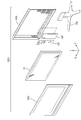
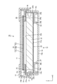
- FIG. 1 is an exploded perspective view showing a schematic configuration of a television receiver according to Embodiment 1 of the present invention.
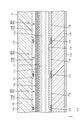
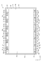
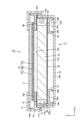
- Cross-sectional view of a liquid crystal panel constituting a liquid crystal display device Plan view of a backlight device constituting a liquid crystal display device AA line sectional view of FIG. BB sectional view of FIG.
- FIGS. 1 A first embodiment of the present invention will be described with reference to FIGS.
- a liquid crystal display device 10 and a television receiver 10TV using the same are illustrated.
- a part of each drawing shows an X axis, a Y axis, and a Z axis, and each axis direction is drawn to be a direction shown in each drawing.
- the upper side shown in FIGS. 4 and 5 is the front side, and the lower side is the back side.
- a television receiver 10TV includes a liquid crystal display device 10 having a substantially horizontally long overall shape, and both front and back cabinets 10Ca and 10Cb that are accommodated so as to sandwich the liquid crystal display device 10.
- a power source 10P a tuner (reception unit) 10T that receives a television signal
- a stand 10S a stand 10S.
- the liquid crystal display device 10 includes a liquid crystal panel (display panel) 11 that displays an image, and a backlight device (illumination device) 12 that supplies light for display to the liquid crystal panel 11. These are integrally held by a frame-like bezel 13 or the like.
- the liquid crystal panel 11 is interposed between a pair of transparent (excellent) substrates 11a and 11b and both the substrates 11a and 11b, and the optical characteristics change with application of an electric field.
- a liquid crystal layer 11c containing liquid crystal molecules as a substance, and both substrates 11a and 11b are bonded together by a sealing agent (not shown) while maintaining a cell gap corresponding to the thickness of the liquid crystal layer 11c.
- the front side (front side) is a CF substrate (counter substrate) 11a
- the back side (back side) is an array substrate (thin film transistor substrate, active matrix substrate) 11b.
- Polarizing plates 11d and 11e are attached to the outer surfaces of both substrates 11a and 11b, respectively.
- a large number of TFTs (Thin Film Transistors) 11f and pixel electrodes 11g, which are switching elements, are arranged in a matrix on the inner surface side of the display area of the array substrate 11b, and around the TFTs 11f and the pixel electrodes 11g.
- a large number of gate wirings and source wirings (both not shown) in a lattice shape are arranged so as to surround them.
- a color filter 11h comprising three colored portions 11hR, 11hG, and 11hB exhibiting red (R), green (G), and blue (B).
- R red
- G green
- B blue
- each of the coloring portions 11hR, 11hG, and 11hB constituting the color filter 11h selectively transmits light of each color (each wavelength).
- Each of the colored portions 11hR, 11hG, and 11hB is manufactured, for example, by containing a predetermined pigment or dye in the base material, and exhibits a specific color corresponding to the pigment or dye.
- Each of the coloring portions 11hR, 11hG, and 11hB constituting the color filter 11h is arranged in a matrix along the X-axis direction (row direction) and the Y-axis direction (column direction), and each is arranged in an array substrate. It is arranged to overlap each pixel electrode 11g on the 11b side in a plan view. Between the colored portions 11hR, 11hG, and 11hB constituting the color filter 11h, a light shielding portion (black matrix, light shielding region) 11i for preventing color mixture is formed.
- One pixel PX which is a display unit is configured.
- the pixel PX includes a red pixel RPX having a red coloring portion 11hR, a green pixel GPX having a green coloring portion 11hG, and a blue pixel BPX having a blue coloring portion 11hB.
- an overcoat film 11k is provided so as to overlap the inside.
- the overcoat film 11k is formed in a solid shape over almost the entire area on the inner surface of the CF substrate 11a.
- a counter electrode 11j is provided so as to overlap the inside.
- the counter electrode 11j is formed in a solid shape over almost the entire area of the inner surface of the CF substrate 11a. Since the counter electrode 11j is always kept at a constant reference potential, when a potential is supplied to each pixel electrode 11g connected to each TFT 11f as each TFT 11f is driven, each pixel electrode 11g A potential difference occurs between the two.
- the alignment state of the liquid crystal molecules contained in the liquid crystal layer 11c changes based on the potential difference generated between the counter electrode 11j and each pixel electrode 11g, and the polarization state of the transmitted light changes accordingly.
- the transmitted light amount is individually controlled for each color pixel RPX, GPX, BPX, and a predetermined color image is displayed. Note that alignment films 11l and 11m for aligning liquid crystal molecules contained in the liquid crystal layer 11c are formed on the innermost sides of both the substrates 11a and 11b in contact with the liquid crystal layer 11c, respectively.
- the backlight device 12 includes a chassis 14 having a substantially box shape having a light emitting portion 14 b that opens toward the front side (the liquid crystal panel 11 side), and a light emitting portion of the chassis 14.
- An optical member (optical sheet) 15 disposed so as to cover the (opening) 14b, and a frame 16 that supports the optical member 15 from the back side.
- a red laser light source 17, a blue laser light source 18 and a green LED light source 19 which are light sources, a laser light source substrate 20 on which the red laser light source 17 and the blue laser light source 18 are mounted, and a green LED light source 19.
- the light guide plate 22 that guides the light from each of the light sources 17 to 19 to the optical member 15 (liquid crystal panel 11), and the reflection that is laminated on the back side of the light guide plate 22
- a sheet 23 and a light guide plate support member 24 interposed between the reflection sheet 23 and the chassis 14 and supporting the light guide plate 22 from the back side are provided.
- the red laser light source 17 is provided with a vertical stripe pattern
- the blue laser light source 18 is provided with a horizontal stripe pattern
- the green LED light source 19 is provided with an oblique stripe pattern.
- a laser light source substrate 20 and an LED light source substrate 21 are arranged at both ends in the short side direction (Y-axis direction), and light from each of the light sources 17 to 19 is guided to the light guide plate.
- the edge light type (side light type) is a double-sided light incident type in which light is incident on both sides from the side 22.
- the chassis 14 is made of metal, and as shown in FIGS. 3 and 4, as in the liquid crystal panel 11, a bottom part 14 a that is substantially horizontally long and a side part 14 c that rises from the outer end of each side of the bottom part 14 a. As a whole, it has a shallow, generally box shape that opens toward the front side.
- the long side direction of the chassis 14 (bottom part 14a) coincides with the X-axis direction (horizontal direction), and the short side direction thereof coincides with the Y-axis direction (vertical direction).
- the frame 16 and the bezel 13 can be fixed to the side portion 14c.
- the optical member 15 covers the light emitting portion 14 b of the chassis 14 and is disposed between the liquid crystal panel 11 and the light guide plate 22. That is, it can be said that the optical member 15 is arranged on the exit side of the light emission path with respect to the light sources 17 to 19.
- the optical member 15 has a sheet shape, and a total of three optical members 15 are provided.
- the optical member 15 includes a microlens sheet 15a that imparts an isotropic condensing function to light, a prism sheet 15b that imparts an anisotropic condensing function to light, and a reflective type that reflects and reflects light. And a polarizing sheet 15c.
- the optical member 15 is laminated from the back side in the order of the microlens sheet 15 a, the prism sheet 15 b, and the reflective polarizing sheet 15 c, and their outer edge portions are placed on the front side of the frame 16.
- the optical member 15 is opposed to the light guide plate 22 on the front side, that is, on the light emitting side, with an interval corresponding to the frame 16 (a frame-like portion 16a described later in detail).
- the frame 16 has a horizontally long frame-like portion 16 a extending along the outer peripheral edge portion of the light guide plate 22 and the optical member 15.
- the frame-shaped portion 16a receives and supports the outer peripheral edge of the optical member 15 from the back side over substantially the entire circumference, and supports the outer peripheral edge of the light guide plate 22 from the front side over the entire circumference.
- Frame side reflection sheets 25 that reflect light are respectively attached to the opposite surfaces of the long side portions of the frame-like portion 16a to the back side surfaces (the light guide plate 22 and the light sources 17 to 19).
- the frame 16 has a liquid crystal panel support portion 16b that protrudes from the frame-shaped portion 16a toward the front side and supports the outer peripheral edge portion of the liquid crystal panel 11 from the back side.
- the red laser light source 17 has a red semiconductor laser element that emits red laser light.
- the blue laser light source 18 includes a blue semiconductor laser element that emits blue laser light.
- the laser beams of the respective colors emitted from the red laser light source 17 and the blue laser light source 18 are coherent lights having the same phase and wavelength, respectively, and have a smaller divergence angle than green light emitted from a green LED light source 19 described later. Strong straightness.
- the color laser light emitted from the red laser light source 17 and the blue laser light source 18 is superior in color purity as compared to the light of each color emitted from a general red LED light source or blue LED light source.
- the red laser light source 17 and the blue laser light source 18 are each mounted on a laser light source substrate 20 described below on the side opposite to the light emitting surface thereof, and are of a so-called top surface emitting type.
- the laser light source substrate 20 has a plate shape extending along the long side direction of the chassis 14, and one side of the long side (the upper side shown in FIG. 3). It is attached to 14c.
- a mounting surface 20 a on which the red laser light source 17 and the blue laser light source 18 are mounted is opposed to one end surface on the long side of the light guide plate 22.
- a wiring pattern (not shown) for supplying power to the red laser light source 17 and the blue laser light source 18 is patterned on the mounting surface 20a of the laser light source substrate 20, and a plurality of red laser light sources 17 and blue lasers are provided.
- the light sources 18 are mounted so as to be alternately arranged at intervals along the X-axis direction.
- the plurality of red laser light sources 17 and blue laser light sources 18 have two intervals between adjacent ones, and those arranged at a relatively narrow interval constitute one set. . Accordingly, the distance between the red laser light source 17 and the blue laser light source 18 that form different sets is relatively wide.
- the green LED light source 19 has a green semiconductor element (green LED element) that emits green light, as shown in FIGS. 3 and 5.
- Green light emitted from the green LED light source 19 is incoherent light, and has a larger divergence angle and weaker straightness than the laser beams of the respective colors emitted from the red laser light source 17 and the blue laser light source 18 described above.
- the green LED light source 19 has a luminous efficiency that is approximately twice as high as that of a general green laser light source, and high luminance can be obtained with low power consumption. Further, the green LED light source 19 is mounted on the LED light source substrate 21 described below on the surface opposite to the light emitting surface of the green LED light source 19, and is a so-called top surface light emitting type.
- the LED light source substrate 21 has a plate shape extending along the long side direction of the chassis 14, and the other side of the long side (the lower side shown in FIG. 3). It is attached to the part 14c.
- the mounting surface 21 a on which the green LED light source 19 is mounted is opposed to the other end surface on the long side of the light guide plate 22.
- a wiring pattern (not shown) for supplying power to the green LED light source 19 is patterned on the mounting surface 21a of the LED light source substrate 21, and a plurality of green LED light sources 19 are spaced along the X-axis direction. It is implemented in a line-up form.
- the interval between adjacent ones is made wider than the arrangement range in the X-axis direction in the red laser light source 17 and the blue laser light source 18 that form the same set. Then, the plurality of green LED light sources 19 are arranged in an offset (unaligned arrangement) with respect to the red laser light source 17 and the blue laser light source 18 in the X-axis direction.
- the light guide plate 22 is made of a substantially transparent synthetic resin material (for example, acrylic resin such as PMMA or polycarbonate). As shown in FIGS. 4 and 5, the light guide plate 22 has a plate shape that is thicker than the optical member 15 and is housed in the chassis 14 so as to be positioned directly below the liquid crystal panel 11 and the optical member 15. . As shown in FIG. 3, the light guide plate 22 has a horizontally long substantially square shape when viewed in a plane, like the optical member 15. Of the outer peripheral end faces of the light guide plate 22, one end face on the long side (the upper side shown in FIG. 3) faces each light emitting face of the red laser light source 17 and the blue laser light source 18 and the laser light of each color enters.
- a substantially transparent synthetic resin material for example, acrylic resin such as PMMA or polycarbonate
- the laser light incident part 22a is provided, and the number of installation and the arrangement interval thereof are the same as the number of installation groups of the red laser light source 17 and the blue laser light source 18 and the arrangement interval between the groups.
- the formation range in the X-axis direction substantially coincides with the arrangement range of the red laser light source 17 and the blue laser light source 18 forming one set.
- the other end face (the lower side shown in FIG. 3) on the long side faces the light emitting face of the green LED light source 19 (facing directly), and the LED incident light is incident on the green light.
- It has the part 22b, and the installation number and arrangement interval are the same as the installation number and arrangement interval of the green LED light source 19.
- the LED light incident part 22 b has a wider formation range in the X-axis direction than the arrangement range of the green LED light source 19. The reason is that the divergence angle of the green light emitted from the green LED light source 19 is larger than the divergence angle of the laser light sources 17 and 18.
- the light guide plate 22 has a light-emitting plate surface 22 c that emits light toward the liquid crystal panel 11 and the optical member 15, of the pair of front and back plate surfaces facing the front side.
- the plate surface facing the back side is the light output opposite plate surface 22d opposite to the light output plate surface 22c.
- the light guide plate 22 introduces the light emitted from the light sources 17 to 19 along the Y-axis direction from the light incident portions 22a and 22b and propagates the light in the Z-axis direction after internally propagating the light. And has a function of emitting light from the light exit plate surface 22c toward the optical member 15 side (front side, light emission side).
- the reflection sheet 23 is arranged so as to cover the light output opposite plate surface 22 d of the light guide plate 22.
- the reflection sheet 23 is excellent in light reflectivity, and can efficiently start up light leaking from the light output opposite plate surface 22d of the light guide plate 22 toward the front side (light output plate surface 22c).
- the reflection sheet 23 has an outer shape that is slightly larger than the light guide plate 22, and both end portions on the long side protrude from the light incident portions 22 a and 22 b of the light guide plate 22 toward the light sources 17 to 19, respectively. It is arranged with.
- the light guide plate support members 24 are made of synthetic resin, and as shown in FIGS. 4 and 5, a pair of light guide plate support members 24 are provided so as to support both ends on the long side of the light guide plate 22 from the back side.
- the light guide plate support member 24 is disposed so as to be interposed between the bottom portion 14a of the chassis 14 and the reflection sheet 23, and the light guide plate 22 is lifted from the bottom portion 14a so as not to be in direct contact with the bottom portion 14a. I support it.
- the light guide plate support member 24 includes a main body portion 24 a that contacts the reflection sheet 23, and a pair of leg portions 24 b that protrude from both end portions of the main body portion 24 a and contact the bottom portion 14 a of the chassis 14.
- FIG. 6 shows emission spectra for the light sources 17 to 19, where the horizontal axis of the figure is the wavelength (unit is “nm”), and the left vertical axis of the figure is the emission intensity (unit is the unit). "W / nm”).
- the emission spectrum of the red laser light source 17 is indicated by a thin broken line
- the emission spectrum of the blue laser light source 18 is indicated by a thin two-dot chain line
- the emission spectrum of the green LED light source 19 is indicated by a thin one-dot chain line.
- the red laser light source 17 emits red laser light having an emission spectrum having a main emission wavelength of 630 nm and a half width (full width at half maximum) of 2 nm.
- the blue laser light source 18 emits blue laser light having an emission spectrum having a main emission wavelength of 441 nm and a half width of 2 nm.
- the blue laser light source 18 has a light emission intensity (0.055 W / nm) at the main light emission wavelength larger than the light emission intensity (0.037 W / nm) of the red laser light source 17.
- the green LED light source 19 emits green light having an emission spectrum having a main emission wavelength of about 534 nm and a half width of about 18 nm.
- the green LED light source 19 has a light emission intensity (0.0018 W / nm) at the main light emission wavelength that is much smaller than the same light emission intensity of each of the red laser light source 17 and the blue laser light source 18, and has a half-value width of the light emission spectrum. It is much wider than the half width of each of the red laser light source 17 and the blue laser light source 18.
- the red laser light emitted from the red laser light source 17 and the blue laser light emitted from the blue laser light source 18 have little wavelength range interference with each other and are emitted from the green LED light source 19.
- the wavelength range hardly interferes with green light. Thereby, the color purity of each color related to the illumination light of the backlight device 12 becomes sufficiently high.
- the green LED light source 19 has better light emission efficiency than a general green laser light source that emits green laser light, high luminance can be obtained with low power consumption.
- FIG. 6 shows a transmission spectrum for each of the colored portions 11hR, 11hG, and 11hB.
- the horizontal axis of FIG. 6 indicates the wavelength (unit: “nm”), and the vertical axis on the right side of FIG. Rate (unit is "%").
- the transmission spectrum of the red colored portion 11hR is indicated by a thick broken line
- the transmission spectrum of the blue colored portion 11hB is indicated by a thick two-dot chain line
- the transmission spectrum of the green colored portion 11hG is indicated by a thick one-dot chain line.
- the red colored portion 11hR exhibiting red color selectively transmits light in the red wavelength region (about 600 nm to about 780 nm), that is, red light, and has a wavelength that is a half value of a peak included in the transmission spectrum. Is configured to be 595 nm or more.
- the “wavelength at half peak value” is a wavelength at half the spectral transmittance value (maximum value) at the peak wavelength (634 nm) of the transmission spectrum.
- the blue colored portion 11hB exhibiting blue is selectively transmitting light in the blue wavelength region (about 420 nm to about 500 nm), that is, blue light, and the peak wavelength included in the transmission spectrum is 468 nm.
- the half width of the peak is about 90 nm.
- the green colored portion 11hG exhibiting green is selectively transmitting light in the green wavelength region (about 500 nm to about 570 nm), that is, green light, and the peak wavelength included in the transmission spectrum is 522 nm. In addition, the half width of the peak is about 96 nm.
- the green coloring portion 11hG has a partially overlapping transmission spectrum with respect to both the red coloring portion 11hR and the blue coloring portion 11hB, but the overlapping amount with the blue coloring portion 11hB is a red coloring portion. It is larger than the amount of overlap with 11hR. Furthermore, the green coloring portion 11hG has a relationship in which the transmission spectrum hardly overlaps with the emission spectrum of the red laser light source 17, but relatively overlaps with the emission spectrum of the blue laser light source 18. For this reason, the green colored portion 11hG has a tendency to transmit blue laser light more easily than red laser light, and there is a concern that the color purity of the green transmitted light in the liquid crystal panel 11 may be reduced due to this. Is done.
- the ratio of the transmitted light amount at the emission wavelength of the blue laser light source 18 to the accumulated transmitted light amount over the entire wavelength region is greater than 0% and greater than 4%. Is also small. That is, the green coloring portion 11hG transmits blue light having a wavelength of 441 nm, which is the emission wavelength of the blue laser light source 18, but the ratio relating to the transmitted light amount of blue light having the wavelength of 441 nm is smaller than 4%. It is configured.
- the accumulated transmitted light amount over the entire wavelength region in the green colored portion 11hG corresponds to the total area in the transmission spectrum of the green colored portion 11hG shown in FIG.
- the amount of blue laser light transmitted through the green coloring portion 11hG is sufficiently reduced as compared with a case where the ratio is 4% or more.
- the color purity concerning the green transmitted light in the liquid crystal panel 11 can be kept sufficiently high.
- the light source of the backlight device 12 is, for example, a blue LED element that emits blue light, a green phosphor that emits green light using the blue light of the blue LED element as excitation light, and blue
- the color purity of the green transmitted light of the liquid crystal panel 11 is equivalent to the case where a white LED light source including a red phosphor that emits red light using blue light of the LED element as excitation light is used.
- the ratio can be made larger than 0% and smaller than 4%, the color relating to the green transmitted light in the liquid crystal panel 11 in comparison with the case where the white LED light source is used as the light source of the backlight device 12. It can be said that the purity can be kept relatively high. More preferably, the green colored portion 11hG has a ratio of 1.41%. In this way, the amount of blue laser light transmitted through the green coloring portion 11hG is further reduced, and the color purity of the green transmitted light in the liquid crystal panel 11 can be further increased.
- the above-described embodiment relates to how the color gamut relating to the green transmitted light in the liquid crystal panel changes when the configuration of the light source of the backlight device or the green coloring portion of the liquid crystal panel is changed.
- the following comparative experiment was conducted.
- the case where a white LED light source is used as the light source of the backlight device is set as Comparative Example 1, and the emission wavelength (441 nm) of the blue laser light source 18 with respect to the accumulated transmitted light amount over the entire wavelength region related to the green colored portion of the liquid crystal panel.
- the ratio of the amount of transmitted light at 4% is taken as Comparative Example 2, and the ratio of the amount of transmitted light at the emission wavelength of the blue laser light source 18 to the cumulative amount of transmitted light over the entire wavelength region relating to the green colored portion 11hG of the liquid crystal panel 11
- the ratio is 1.41%.
- the white LED light source provided in Comparative Example 1 is a blue LED element that emits blue light, a green phosphor that emits green light using the blue light of the blue LED element as excitation light, and the blue light of the blue LED element as excitation light. And a red phosphor that emits red light.
- the liquid crystal panel provided in Comparative Example 2 has the same configuration as the liquid crystal panel provided in the example except for the green colored portion.
- the liquid crystal panel 11 provided in the embodiment is the same as that described before this paragraph.
- each backlight apparatus with which the comparative example 2 and an Example are provided is the same as what was demonstrated before this paragraph.
- the chromaticity of the transmitted light of the liquid crystal panel which comprises each liquid crystal display device which concerns on the above comparative examples 1 and 2 and an Example was measured, respectively, and the result is shown in FIG.7 and FIG.8.
- the chromaticity of the transmitted light in the liquid crystal panel is that the red color is displayed on the liquid crystal panel (the red tone value is maximized and the green and blue tone values are minimized) and the green color is monochromatically displayed. State (maximum green gradation value and minimum red and blue gradation values), and blue display condition (maximum blue gradation value, red and green gradations)
- the light transmitted through the liquid crystal panel is measured by a spectrocolorimeter or the like.
- FIG. 7 shows BT.
- FIG. 8 is a CIE 1976 chromaticity diagram, where the horizontal axis represents the u ′ value and the vertical axis represents the v ′ value. 8 plots the respective u ′ and v ′ values described in the table of FIG. Each chromaticity region of the 2020 standard, Comparative Examples 1 and 2 and Examples is shown. In FIG.
- each chromaticity of R, G, B according to the 2020 standard is shown by a square plot, and the chromaticity region is shown by a thick solid line.
- the chromaticities of R, G, and B according to Comparative Example 1 are indicated by a triangular plot, and the chromaticity region is indicated by a one-dot chain line.
- the chromaticities of R, G, and B according to Comparative Example 2 are indicated by x-type plots, and the chromaticity regions are indicated by broken lines.
- each chromaticity of R, G, and B according to the embodiment is shown by a rhombus plot, and the chromaticity region is shown by a thin solid line.
- Comparative Examples 1 and 2 based on the description of FIG. 7 and FIG. Although each of the red and blue color gamuts in the 2020 standard is relatively wider than Comparative Example 1, the green color gamut is the same. This is because the comparative example 2 uses the red laser light source 17, the blue laser light source 18, and the green LED light source 19 as the light source of the backlight device.
- the comparative example 2 is a white LED light source like the comparative example 1. The color purity of red and blue is relatively higher than in the case of using.
- the ratio of the transmitted light amount at the emission wavelength of the blue laser light source 18 to the accumulated transmitted light amount over the entire wavelength region related to the green coloring portion 11hG of the liquid crystal panel 11 is 1.41%. This is because the amount of blue laser light transmitted through the green colored portion 11hG is reduced by being smaller than the same ratio (4%), and the green color purity of the example is relatively higher than that of the comparative example 2. Yes. From the above experimental results, when the above ratio is at least smaller than 4% of Comparative Example 2, the amount of blue laser light transmitted through the green coloring portion 11hG is reduced accordingly, and the green light amount is reduced as the amount of light decreases. It can be said that the color purity tends to be high (wide color gamut).
- the backlight device 12 has a diffuse reflection member 26 for diffusing and reflecting the laser beams of the respective colors propagating through the light guide plate 22.
- the diffuse reflection member 26 is integrally provided on the LED light source substrate 21.
- the diffuse reflection member 26 is disposed so as to be sandwiched between the light guide plate 22 and the LED light source substrate 21 in the Y-axis direction, and is disposed adjacent to the green LED light source 19 in the X-axis direction. .
- the diffuse reflection member 26 is opposite to the laser incident portion 22a on the other end surface (the lower side shown in FIG. 3) of the long side facing the LED light source substrate 21 in the outer peripheral end surface of the light guide plate 22.
- the laser incident light opposite portion 22e which is a portion located on the side.
- a plurality of the diffuse reflection members 26 and the laser incident light opposite portions 22e are arranged on the other end face of the light guide plate 22 so as to be alternately arranged along with the LED incident portions 22b along the X-axis direction.
- the diffuse reflection member 26 and the laser incident light opposite portion 22e are substantially equal to the arrangement range in the X-axis direction in the red laser light source 17 and the blue laser light source 18 that form one set in the X-axis direction.
- the red laser light and the blue laser light emitted from the red laser light source 17 and the blue laser light source 18 enter the laser incident part 22a, the light enters the light guide plate 22 and enters the laser beam. It reaches the laser incident light opposite portion 22e located on the opposite side to the portion 22a.
- the red laser beam and the blue laser beam that have reached the laser incident light opposite portion 22e are diffused and reflected by the diffuse reflection member 26, and then proceed toward the laser incident portion 22a while diffusing in the light guide plate 22.
- the diffuse reflection member 26 disposed on the same side as the green LED light source 19 in the Y-axis direction serves as a pseudo light source that emits red and blue diffused light having a divergence angle equal to or greater than that of the green LED light source 19.
- the luminance uniformity of the emitted light is high within the surface of the light output plate surface 22c.
- the LED light source substrate 21 and the diffuse reflection member 26 are preferably arranged on the lower side in the vertical direction with respect to the light guide plate 22. By doing so, the diffuse reflection member 26 can be continuously held in close contact with the laser incident light opposite portion 22e by utilizing the weight of the light guide plate 22, and the laser incident light opposite portion 22e and the diffuse reflection can be kept.
- the liquid crystal display device (display device) 10 of the present embodiment includes the red laser light source 17 that emits red laser light, the blue laser light source 18 that emits blue laser light, and the green LED light source 19 that emits green light. , And at least a color filter 11h composed of a plurality of colored portions 11hR, 11hG, and 11hB that exhibit blue, green, and red, and uses light from the backlight device 12.
- a green colored portion 11hG that exhibits green in the color filter 11h has a transmitted light amount at the emission wavelength of the blue laser light source 18 with respect to the accumulated transmitted light amount over the entire wavelength region.
- the ratio is configured to be greater than 0% and less than 4%.
- the red laser light emitted from the red laser light source 17 provided in the backlight device 12 and the blue laser light emitted from the blue laser light source 18 have little wavelength range interference with each other, and are emitted from the green LED light source 19. It is assumed that the wavelength range hardly interferes with the green light to be emitted. Thereby, the color purity of each color becomes sufficiently high. Moreover, since the green LED light source 19 has better luminous efficiency than a green laser light source that emits green laser light, high luminance can be obtained with low power consumption.
- the color filter 11h provided in the liquid crystal panel 11 includes a plurality of coloring portions 11hR, 11hG, and 11hB that exhibit at least blue, green, and red, and light of each color emitted from the red laser light source 17, the blue laser light source 18, and the green LED light source 19.
- the green colored portion 11hG that exhibits green in the color filter 11h has a relationship in which the transmission spectrum overlaps the emission spectrum of the blue laser light source 18 more than the emission spectrum of the red laser light source 17. For this reason, the green colored portion 11hG exhibiting green has a tendency to transmit blue laser light more easily than red laser light, and as a result, the color purity of the green transmitted light in the liquid crystal panel 11 decreases.
- the green colored portion 11hG that exhibits green is configured such that the ratio of the transmitted light amount at the emission wavelength of the blue laser light source 18 to the accumulated transmitted light amount over the entire wavelength region is greater than 0% and less than 4%. Therefore, as compared with the case where the ratio is 4% or more, the amount of blue laser light transmitted through the green colored portion 11hG exhibiting green is sufficiently reduced. Thereby, the color purity concerning the green transmitted light in the liquid crystal panel 11 can be kept sufficiently high.
- the light source of the backlight device 12 is, for example, a blue LED element that emits blue light, a green phosphor that emits green light using the blue light of the blue LED element as excitation light, and blue
- the color purity of the green transmitted light of the liquid crystal panel 11 is equivalent to the case where a white LED light source including a red phosphor that emits red light using blue light of the LED element as excitation light is used. Therefore, by making the ratio larger than 0% and smaller than 4%, the color relating to the green transmitted light in the liquid crystal panel 11 in comparison with the case where the white LED light source is used as the light source of the backlight device 12. It can be said that the purity can be kept relatively high.
- the ratio of the green colored portion 11hG exhibiting green is 1.41%. In this way, the amount of blue laser light transmitted through the green colored portion 11hG that exhibits green can be further reduced, and the color purity of the green transmitted light in the liquid crystal panel 11 can be further increased.
- the blue laser light source 18 has an emission wavelength of 441 nm ⁇ 20 nm. In this way, the color purity relating to the blue transmitted light in the liquid crystal panel 11 can be sufficiently increased.
- the television receiver 10TV includes the liquid crystal display device 10. According to the television receiver 10TV having such a configuration, the color purity of light of each color related to the liquid crystal display device 10 is improved, so that a television image with high display quality can be displayed.
- the ratio of the transmitted light amount at the emission wavelength of the blue laser light source to the accumulated transmitted light amount over the entire wavelength region related to the green colored portion of the liquid crystal panel is 1.41%.
- the specific value of the above ratio can be changed as appropriate as long as it is larger than 0% and smaller than 4%, but it is more likely to be in a range larger than 1.41% and smaller than 4%. More preferably, the range is larger than 1.41% and smaller than 2.81%.
- specific emission spectra (numerical values such as the main emission wavelength and the half-value width) relating to the red laser light source, the blue laser light source, and the green LED light source can be appropriately changed.
- the main emission wavelength of the blue laser light source may be larger or smaller than 441 nm, and specifically, is preferably in the range of 441 nm ⁇ 20 nm.
- specific transmission spectra (numerical values such as peak wavelength and half-value width) relating to the R, G, and B colored portions constituting the color filter can be appropriately changed.
- the diffuse reflection member is provided on the LED light source substrate constituting the backlight device, but the diffuse reflection member may be integrally provided on the light guide plate. It is also possible to omit the diffuse reflection member.
- the color filter of the liquid crystal panel is exemplified as a three-color configuration of red, green, and blue. The present invention can also be applied to those provided with the color filter.
- the specific configuration of the backlight device can be changed. For example, a light guide rod that guides the light of each laser light source may be installed separately from the light guide plate, and the light from the light guide rod may be incident on the end face of the light guide plate.
- the double-sided light input type edge light type backlight device is illustrated, but an edge light type backlight device such as a single side light incident type may be used. Further, it may be a direct type backlight device.
- an edge light type backlight device such as a single side light incident type may be used. Further, it may be a direct type backlight device.
- FFS Ringe Field Switching
- planar shape of the liquid crystal display device (liquid crystal panel or backlight device) is a horizontally long square is shown.
- the planar shape of the liquid crystal display device is a vertically long square, square, long It may be a circular shape, an elliptical shape, a circular shape, a trapezoidal shape, a shape having a partially curved surface, or the like.
- SYMBOLS 10 Liquid crystal display device (display device), 10TV ... Television receiver, 11 ... Liquid crystal panel (display panel), 11h ... Color filter, 11hB ... Blue colored part (colored part), 11hG ... Green colored part (colored part), 11hR: Red colored portion (colored portion), 12 ... Backlight device (illuminating device), 17 ... Red laser light source, 18 ... Blue laser light source, 19 ... Green LED light source
Landscapes
- Physics & Mathematics (AREA)
- Engineering & Computer Science (AREA)
- General Physics & Mathematics (AREA)
- Multimedia (AREA)
- Signal Processing (AREA)
- Nonlinear Science (AREA)
- Theoretical Computer Science (AREA)
- Chemical & Material Sciences (AREA)
- Mathematical Physics (AREA)
- Crystallography & Structural Chemistry (AREA)
- General Engineering & Computer Science (AREA)
- Optics & Photonics (AREA)
- Liquid Crystal (AREA)
- Planar Illumination Modules (AREA)
- Devices For Indicating Variable Information By Combining Individual Elements (AREA)
- Video Image Reproduction Devices For Color Tv Systems (AREA)
- Transforming Electric Information Into Light Information (AREA)
Abstract
本発明における液晶表示装置は、赤色レーザ光を発する赤色レーザ光源と、青色レーザ光を発する青色レーザ光源と、緑色光を発する緑色LED光源1と、を少なくとも有するバックライト装置と、少なくとも青色、緑色、赤色を呈する複数の着色部からなるカラーフィルタを少なくとも有し、バックライト装置からの光を利用して表示を行う液晶パネルと、を備え、カラーフィルタのうち緑色を呈する緑色着色部は、全波長領域にわたる累積透過光量に対する青色レーザ光源の発光波長における透過光量の比率が0%よりも大きく且つ4%よりも小さくなるよう構成される。
Description
本発明は、表示装置及びテレビ受信装置に関する。
従来の液晶表示装置の一例として下記特許文献1に記載されたものが知られている。この特許文献1に記載された液晶表示装置は、第1の光を発する第1の光源と、第1の光を入射して第1の線状光に変換する第1の導光棒と、第1の光よりも大きな発散角を有する第2の光を発する第2の光源と、第2の光を第1の線状光と同一方向に延びる第2の線状光に変換する第2の導光棒と、を備える面光源装置を有する。また、この面光源装置は、第1及び第2の導光棒より面状光の出射側に配置される反射バーと、第1の導光棒、第2の光源、第2の導光棒及び反射バーを収容し、内壁が反射面となる箱形状であって面状光の出射側の面に開口部を有する反射部と、を備える。第1及び第2の線状光は、反射バー及び反射面で反射され、開口部から反射部の外部に出射される。
(発明が解決しようとする課題)
上記した特許文献1に記載された液晶表示装置では、第1の光源として赤色光を発光するレーザー光源が用いられるとともに、第2の光源として青緑色光を発光する青緑色LED素子を有するLED光源が用いられている。このような構成によれば、レーザ光源が発光する赤色光は、色純度が改善されるものの、青色光及び緑色光に係る色純度に関しては、十分な色純度が得られない可能性があった。
上記した特許文献1に記載された液晶表示装置では、第1の光源として赤色光を発光するレーザー光源が用いられるとともに、第2の光源として青緑色光を発光する青緑色LED素子を有するLED光源が用いられている。このような構成によれば、レーザ光源が発光する赤色光は、色純度が改善されるものの、青色光及び緑色光に係る色純度に関しては、十分な色純度が得られない可能性があった。
本発明は上記のような事情に基づいて完成されたものであって、青色光及び緑色光の色純度を向上させることを目的とする。
(課題を解決するための手段)
本発明の表示装置は、赤色レーザ光を発する赤色レーザ光源と、青色レーザ光を発する青色レーザ光源と、緑色光を発する緑色LED光源と、を少なくとも有する照明装置と、少なくとも青色、緑色、赤色を呈する複数の着色部からなるカラーフィルタを少なくとも有し、前記照明装置からの光を利用して表示を行う表示パネルと、を備え、前記カラーフィルタのうち緑色を呈する着色部は、全波長領域にわたる累積透過光量に対する前記青色レーザ光源の発光波長における透過光量の比率が0%よりも大きく且つ4%よりも小さくなるよう構成される。
本発明の表示装置は、赤色レーザ光を発する赤色レーザ光源と、青色レーザ光を発する青色レーザ光源と、緑色光を発する緑色LED光源と、を少なくとも有する照明装置と、少なくとも青色、緑色、赤色を呈する複数の着色部からなるカラーフィルタを少なくとも有し、前記照明装置からの光を利用して表示を行う表示パネルと、を備え、前記カラーフィルタのうち緑色を呈する着色部は、全波長領域にわたる累積透過光量に対する前記青色レーザ光源の発光波長における透過光量の比率が0%よりも大きく且つ4%よりも小さくなるよう構成される。
照明装置に備わる赤色レーザ光源から発せられる赤色レーザ光と、青色レーザ光源から発せられる青色レーザ光と、は、互いに波長範囲が干渉することが殆ど無く、且つ緑色LED光源から発せられる緑色光に対しても波長範囲が干渉することが殆ど無いものとされる。これにより、各色の色純度が十分に高いものとなる。しかも、緑色LED光源は、緑色レーザ光を発する緑色レーザ光源に比べると、発光効率が良好なので、低消費電力で高輝度が得られる。
表示パネルに備わるカラーフィルタは、少なくとも青色、緑色、赤色を呈する複数の着色部からなり、赤色レーザ光源、青色レーザ光源及び緑色LED光源から発せられる各色の光を透過することで、所定のカラー画像を表示することが可能とされる。カラーフィルタのうち緑色を呈する着色部は、その透過スペクトルが赤色レーザ光源の発光スペクトルよりも青色レーザ光源の発光スペクトルに対してより大きく重なる関係を有する。このため、緑色を呈する着色部は、赤色レーザ光よりも青色レーザ光を透過し易い傾向を有しており、それに起因して表示パネルにおける緑色の透過光に係る色純度が低下することが懸念される。その点、緑色を呈する着色部は、全波長領域にわたる累積透過光量に対する青色レーザ光源の発光波長における透過光量の比率が0%よりも大きく且つ4%よりも小さくなるよう構成されているから、仮に上記比率が4%以上とされる場合に比べると、緑色を呈する着色部を透過する青色レーザ光の光量が十分に減少する。これにより、表示パネルにおける緑色の透過光に係る色純度を十分に高く保つことができる。
ここで、上記比率が4%の場合は、照明装置の光源を、例えば青色光を発する青色LED素子と、青色LED素子の青色光を励起光として緑色光を発する緑色蛍光体と、青色LED素子の青色光を励起光として赤色光を発する赤色蛍光体と、からなる白色LED光源とした場合と、表示パネルの緑色の透過光に係る色純度が同等とされる。従って、上記比率を0%よりも大きく且つ4%よりも小さくすることで、照明装置の光源として白色LED光源を用いた場合との比較において、表示パネルにおける緑色の透過光に係る色純度を相対的に高く保つことができる、と言える。
本発明の実施態様として、次の構成が好ましい。
(1)前記緑色を呈する着色部は、前記比率が1.41%とされる。このようにすれば、緑色を呈する着色部を透過する青色レーザ光の光量がさらに減少し、表示パネルにおける緑色の透過光に係る色純度をより高くすることができる。
(1)前記緑色を呈する着色部は、前記比率が1.41%とされる。このようにすれば、緑色を呈する着色部を透過する青色レーザ光の光量がさらに減少し、表示パネルにおける緑色の透過光に係る色純度をより高くすることができる。
(2)前記青色レーザ光源は、前記発光波長が441nm±20nmとされる。このようにすれば、表示パネルにおける青色の透過光に係る色純度を十分に高くすることができる。
次に、上記課題を解決するために、本発明のテレビ受信装置は、上記記載の表示装置を備える。このような構成のテレビ受信装置によれば、表示装置に係る各色の光の色純度が向上しているから、高い表示品位のテレビ画像を表示することができる。
(発明の効果)
本発明によれば、青色光及び緑色光の色純度を向上させることができる。
本発明によれば、青色光及び緑色光の色純度を向上させることができる。
<実施形態1>
本発明の実施形態1を図1から図8によって説明する。本実施形態では、液晶表示装置10及びそれを用いたテレビ受信装置10TVについて例示する。なお、各図面の一部にはX軸、Y軸及びZ軸を示しており、各軸方向が各図面で示した方向となるように描かれている。また、図4及び図5などに示す上側を表側とし、同図下側を裏側とする。
本発明の実施形態1を図1から図8によって説明する。本実施形態では、液晶表示装置10及びそれを用いたテレビ受信装置10TVについて例示する。なお、各図面の一部にはX軸、Y軸及びZ軸を示しており、各軸方向が各図面で示した方向となるように描かれている。また、図4及び図5などに示す上側を表側とし、同図下側を裏側とする。
本実施形態に係るテレビ受信装置10TVは、図1に示すように、全体として横長の略方形状をなす液晶表示装置10と、当該液晶表示装置10を挟むようにして収容する表裏両キャビネット10Ca,10Cbと、電源10Pと、テレビ信号を受信するチューナー(受信部)10Tと、スタンド10Sと、を備えて構成される。液晶表示装置10は、図4に示すように、画像を表示する液晶パネル(表示パネル)11と、液晶パネル11に表示のための光を供給するバックライト装置(照明装置)12と、を備え、これらが枠状のベゼル13などにより一体的に保持される。
液晶パネル11は、図2に示すように、一対の透明な(透光性に優れた)基板11a,11bと、両基板11a,11b間に介在し、電界印加に伴って光学特性が変化する物質である液晶分子を含む液晶層11cと、を備え、両基板11a,11bが液晶層11cの厚さ分のセルギャップを維持した状態で図示しないシール剤によって貼り合わせられている。一対の基板11a,11bのうち表側(正面側)がCF基板(対向基板)11aとされ、裏側(背面側)がアレイ基板(薄膜トランジスタ基板、アクティブマトリクス基板)11bとされる。両基板11a,11bの外面には、それぞれ偏光板11d,11eが貼り付けられている。アレイ基板11bにおける表示領域の内面側には、スイッチング素子であるTFT(Thin Film Transistor)11f及び画素電極11gが多数個ずつマトリクス状に並んで設けられるとともに、これらTFT11f及び画素電極11gの周りには、格子状をなす多数本ずつのゲート配線及びソース配線(共に図示せず)が取り囲むようにして配設されている。
CF基板11aにおける表示領域の内面側には、図2に示すように、赤色(R),緑色(G),青色(B)を呈する3色の着色部11hR,11hG,11hBからなるカラーフィルタ11hが設けられている。カラーフィルタ11hを構成する各着色部11hR,11hG,11hBは、後に詳しく説明するが、各色(各波長)の光を選択的に透過するものとされる。各着色部11hR,11hG,11hBは、例えば、基材中に所定の顔料または染料を含有させて製造されており、顔料または染料に応じた特定の色を呈するものとされる。カラーフィルタ11hを構成する各着色部11hR,11hG,11hBは、X軸方向(行方向)及びY軸方向(列方向)に沿って行列状に並んで複数ずつ配列されており、それぞれがアレイ基板11b側の各画素電極11gと平面に視て重畳する配置とされている。カラーフィルタ11hを構成する各着色部11hR,11hG,11hB間には、混色を防ぐための遮光部(ブラックマトリクス、遮光領域)11iが形成されている。この液晶パネル11においては、カラーフィルタ11hにおけるR,G,Bの3色の着色部11hR,11hG,11hBと、各着色部11hR,11hG,11hBと対向する3つの画素電極11gと、の組によって表示単位である1つの画素PXが構成されている。画素PXは、赤色着色部11hRを有する赤色画素RPXと、緑色着色部11hGを有する緑色画素GPXと、青色着色部11hBを有する青色画素BPXと、からなる。
カラーフィルタ11hの表面には、図2に示すように、オーバーコート膜11kが内側に重なって設けられている。オーバーコート膜11kは、CF基板11aの内面においてほぼ全域にわたってベタ状に形成されている。オーバーコート膜11kの表面には、対向電極11jが内側に重なって設けられている。対向電極11jは、CF基板11aの内面におけるほぼ全域にわたってベタ状に形成されている。対向電極11jは、常に一定の基準電位に保たれているので、各TFT11fが駆動されるのに伴って各TFT11fに接続された各画素電極11gに電位が供給されると、各画素電極11gとの間に電位差が生じる。そして、対向電極11jと各画素電極11gとの間に生じる電位差に基づいて液晶層11cに含まれる液晶分子の配向状態が変化し、それに伴って透過光の偏光状態が変化し、もって液晶パネル11の透過光量が各色の画素RPX,GPX,BPX毎に個別に制御されて所定のカラー画像が表示されるようになっている。なお、両基板11a,11bにおいて液晶層11cに接する最も内側には、液晶層11cに含まれる液晶分子を配向させるための配向膜11l,11mがそれぞれ形成されている。
バックライト装置12は、図3及び図4に示すように、表側(液晶パネル11側)に向けて開口する光出射部14bを有した略箱型をなすシャーシ14と、シャーシ14の光出射部(開口部)14bを覆う形で配される光学部材(光学シート)15と、光学部材15を裏側から支持するフレーム16と、を備える。さらに、シャーシ14内には、光源である赤色レーザ光源17、青色レーザ光源18及び緑色LED光源19と、赤色レーザ光源17及び青色レーザ光源18が実装されたレーザ光源基板20と、緑色LED光源19が実装されたLED光源基板21と、各光源17~19からの光を導光して光学部材15(液晶パネル11)へと導く導光板22と、導光板22の裏側に積層配置される反射シート23と、反射シート23とシャーシ14との間に介在して導光板22を裏側から支持する導光板支持部材24と、が備えられる。なお、図3では、区別のために赤色レーザ光源17には縦縞の模様を、青色レーザ光源18には横縞の模様を、緑色LED光源19には斜め縞の模様を、それぞれ付している。そして、このバックライト装置12は、その短辺方向(Y軸方向)についての両端部にレーザ光源基板20とLED光源基板21とが配されており、各光源17~19からの光が導光板22に対して両側から入光される両側入光タイプのエッジライト型(サイドライト型)とされる。続いて、バックライト装置12の各構成部品について詳しく説明する。
シャーシ14は、金属製とされ、図3及び図4に示すように、液晶パネル11と同様に横長の略方形状をなす底部14aと、底部14aの各辺の外端からそれぞれ立ち上がる側部14cと、からなり、全体としては表側に向けて開口した浅い略箱型をなしている。シャーシ14(底部14a)は、その長辺方向がX軸方向(水平方向)と一致し、短辺方向がY軸方向(鉛直方向)と一致している。また、側部14cには、フレーム16及びベゼル13が固定可能とされる。
光学部材15は、図4に示すように、シャーシ14の光出射部14bを覆うとともに、液晶パネル11と導光板22との間に介在する形で配されている。つまり、光学部材15は、各光源17~19に対して出光経路の出口側に配されている、と言える。光学部材15は、シート状をなしていて合計で3枚が備えられている。具体的には、光学部材15は、光に等方性集光作用を付与するマイクロレンズシート15aと、光に異方性集光作用を付与するプリズムシート15bと、光を偏光反射する反射型偏光シート15cと、から構成される。光学部材15は、裏側からマイクロレンズシート15a、プリズムシート15b、及び反射型偏光シート15cの順で相互に積層されてそれらの外縁部がフレーム16に対してその表側に載せられている。つまり、光学部材15は、導光板22に対して表側、つまり光出射側にフレーム16(詳しくは後述する枠状部16a)分の間隔を空けて対向状をなしている。
フレーム16は、図4に示すように、導光板22及び光学部材15の外周縁部に沿って延在する横長の枠状部16aを有している。この枠状部16aは、光学部材15の外周縁部をほぼ全周にわたって裏側から受けて支持するとともに、導光板22の外周縁部をほぼ全周にわたって表側から押さえて支持する。枠状部16aにおける両長辺部における裏側の面(導光板22及び各光源17~19)との対向面には、光を反射するフレーム側反射シート25がそれぞれ取り付けられている。また、フレーム16は、枠状部16aから表側に向けて突出するとともに、液晶パネル11における外周縁部を裏側から支持する液晶パネル支持部16bを有している。
赤色レーザ光源17は、図3及び図4に示すように、赤色レーザ光を発する赤色半導体レーザ素子を有する。青色レーザ光源18は、青色レーザ光を発する青色半導体レーザ素子を有する。これら赤色レーザ光源17及び青色レーザ光源18が発する各色のレーザ光は、それぞれ位相及び波長が揃ったコヒーレント光であり、後述する緑色LED光源19から発せられる緑色光に比べると、発散角が小さくて直進性が強い。そして、赤色レーザ光源17及び青色レーザ光源18が発する各色のレーザ光は、一般的な赤色LED光源や青色LED光源が発する各色の光に比べると、色純度が優れている。また、赤色レーザ光源17及び青色レーザ光源18は、自身の発光面とは反対側の面が次述するレーザ光源基板20にそれぞれ実装されており、いわゆる頂面発光型とされる。
レーザ光源基板20は、図3及び図4に示すように、シャーシ14の長辺方向に沿って延在する板状をなしており、長辺側の一方(図3に示す上側)の側部14cに対して取り付けられている。レーザ光源基板20は、赤色レーザ光源17及び青色レーザ光源18が実装された実装面20aが導光板22の長辺側の一方の端面と対向状をなしている。レーザ光源基板20の実装面20aには、赤色レーザ光源17及び青色レーザ光源18に対して給電するための配線パターン(図示せず)がパターニングされるとともに、複数ずつの赤色レーザ光源17及び青色レーザ光源18がX軸方向に沿って間隔を空けて交互に並ぶ形で実装されている。詳しくは、複数ずつの赤色レーザ光源17及び青色レーザ光源18は、隣り合うものの間の間隔が2通りとされており、相対的に狭い間隔で配置されるものが1つの組を構成している。従って、異なる組をなす赤色レーザ光源17及び青色レーザ光源18の間の間隔は、相対的に広くなっている。
緑色LED光源19は、図3及び図5に示すように、緑色光を発する緑色半導体素子(緑色LED素子)を有する。緑色LED光源19が発する緑色光は、インコヒーレント光であり、上記した赤色レーザ光源17及び青色レーザ光源18が発する各色のレーザ光に比べると、発散角が大きくて直進性が弱い。そして、緑色LED光源19は、一般的な緑色レーザ光源に比べると、発光効率が2倍程度優れており、低い消費電力でもって高い輝度が得られる。また、緑色LED光源19は、自身の発光面とは反対側の面が次述するLED光源基板21に実装されており、いわゆる頂面発光型とされる。
LED光源基板21は、図3及び図5に示すように、シャーシ14の長辺方向に沿って延在する板状をなしており、長辺側の他方(図3に示す下側)の側部14cに対して取り付けられている。LED光源基板21は、緑色LED光源19が実装された実装面21aが導光板22の長辺側の他方の端面と対向状をなしている。LED光源基板21の実装面21aには、緑色LED光源19に対して給電するための配線パターン(図示せず)がパターニングされるとともに、複数の緑色LED光源19がX軸方向に沿って間隔を空けて並ぶ形で実装されている。詳しくは、複数の緑色LED光源19は、隣り合うものの間の間隔が、同じ組をなす赤色レーザ光源17及び青色レーザ光源18におけるX軸方向についての配置範囲よりも広くされる。そして、複数の緑色LED光源19は、赤色レーザ光源17及び青色レーザ光源18とはX軸方向についてオフセットした配置(揃わない配置)とされる。
導光板22は、ほぼ透明な合成樹脂材料(例えばPMMAなどのアクリル樹脂やポリカーボネートなど)からなる。導光板22は、図4及び図5に示すように、光学部材15よりも厚みが大きな板状をなすとともに液晶パネル11及び光学部材15の直下に位置する形でシャーシ14内に収容されている。導光板22は、図3に示すように、光学部材15などと同様に平面に視て横長の略方形状をなしている。導光板22の外周端面のうち長辺側の一方(図3に示す上側)の端面は、赤色レーザ光源17及び青色レーザ光源18の各発光面と正対していて各色のレーザ光が入射されるレーザ入光部22aを有しており、その設置数及び配置間隔は赤色レーザ光源17及び青色レーザ光源18の設置組数及び各組間の配置間隔と同一である。レーザ入光部22aは、X軸方向についての形成範囲が1つの組をなす赤色レーザ光源17及び青色レーザ光源18の配置範囲とほぼ一致している。導光板22の外周端面のうち長辺側の他方(図3に示す下側)の端面は、緑色LED光源19の発光面と対向(正対)していて緑色光が入射されるLED入光部22bを有しており、その設置数及び配置間隔は緑色LED光源19の設置数及び配置間隔と同一である。LED入光部22bは、X軸方向についての形成範囲が緑色LED光源19の配置範囲よりも広い。その理由は、緑色LED光源19から発せられる緑色光の発散角が各レーザ光源17,18の同発散角よりも大きい為である。導光板22は、図4及び図5に示すように、表裏一対の板面のうち、表側を向いた板面が、光を液晶パネル11及び光学部材15に向けて出射させる出光板面22cとされ、裏側を向いた板面が出光板面22cとは反対側の出光反対板面22dとされる。以上により、導光板22は、各光源17~19からY軸方向に沿って発せられた光を各入光部22a,22bから導入するとともに、その光を内部で伝播させた後にZ軸方向に沿って立ち上げて出光板面22cから光学部材15側(表側、光出射側)へ向けて出射させる機能を有している。
反射シート23は、図4に示すように、導光板22の出光反対板面22dを覆う形で配される。反射シート23は、光反射性に優れており、導光板22の出光反対板面22dから漏れた光を表側(出光板面22c)に向けて効率的に立ち上げることができる。反射シート23は、導光板22よりも一回り大きな外形を有しており、長辺側の両端部が導光板22の各入光部22a,22bよりも各光源17~19側にそれぞれ突き出す形で配されている。
導光板支持部材24は、合成樹脂製とされ、図4及び図5に示すように、導光板22における長辺側の両端部を裏側からそれぞれ支持する形で一対備えられる。導光板支持部材24は、シャーシ14の底部14aと反射シート23との間に介在する形で配されており、導光板22を底部14aとは直接接することがないよう底部14aから持ち上げた形で支持している。これにより、各光源17~19から発光に伴って生じた熱が各基板20,21を介してシャーシ14に伝達されても、シャーシ14から導光板22へ伝達され難くなっている。導光板支持部材24は、反射シート23に接する本体部24aと、本体部24aの両端部から突出してシャーシ14の底部14aに接する一対の脚部24bと、からなる。
ここで、バックライト装置12に備わる各光源17~19における主発光波長及び発光スペクトルについて図6を用いて詳しく説明する。図6には、各光源17~19に係る発光スペクトルが示されており、同図の横軸が波長(単位は「nm」)とされ、同図の左側の縦軸が発光強度(単位は「W/nm」)とされている。また、図6では、細い破線により赤色レーザ光源17の発光スペクトルを、細い二点鎖線により青色レーザ光源18の発光スペクトルを、細い一点鎖線により緑色LED光源19の発光スペクトルを、それぞれ示している。赤色レーザ光源17は、主発光波長が630nmとされ、半値幅(半値全幅)が2nmとされる発光スペクトルの赤色レーザ光を発する。青色レーザ光源18は、主発光波長が441nmとされ、半値幅が2nmとされる発光スペクトルの青色レーザ光を発する。青色レーザ光源18は、主発光波長における発光強度(0.055W/nm)が、赤色レーザ光源17の同発光強度(0.037W/nm)よりも大きい。緑色LED光源19は、主発光波長が約534nmとされ、半値幅が約18nmとされる発光スペクトルの緑色光を発する。緑色LED光源19は、主発光波長における発光強度(0.0018W/nm)が、赤色レーザ光源17及び青色レーザ光源18のそれぞれの同発光強度よりも遙かに小さく、また発光スペクトルの半値幅が赤色レーザ光源17及び青色レーザ光源18のそれぞれの同半値幅よりも遙かに広い。以上のように、赤色レーザ光源17から発せられる赤色レーザ光と、青色レーザ光源18から発せられる青色レーザ光と、は、互いに波長範囲が干渉することが殆ど無く、且つ緑色LED光源19から発せられる緑色光に対しても波長範囲が干渉することが殆ど無いものとされる。これにより、バックライト装置12の照明光に係る各色の色純度が十分に高いものとなる。しかも、緑色LED光源19は、緑色レーザ光を発する一般的な緑色レーザ光源に比べると、発光効率が良好なので、低消費電力で高輝度が得られる。
次に、液晶パネル11に備わるカラーフィルタ11hの各着色部11hR,11hG,11hBにおける透過スペクトルについて図6を用いて詳しく説明する。図6には、各着色部11hR,11hG,11hBに係る透過スペクトルが示されており、同図の横軸が波長(単位は「nm」)とされ、同図の右側の縦軸が分光透過率(単位は「%」)とされている。また、図6では、太い破線により赤色着色部11hRの透過スペクトルを、太い二点鎖線により青色着色部11hBの透過スペクトルを、太い一点鎖線により緑色着色部11hGの透過スペクトルを、それぞれ示している。赤色を呈する赤色着色部11hRは、赤色の波長領域(約600nm~約780nm)の光、つまり赤色光を選択的に透過するものとされており、その透過スペクトルに含まれるピークの半値となる波長が595nm以上となるよう構成されている。この「ピークの半値となる波長」は、透過スペクトルのピーク波長(634nm)における分光透過率の値(最大値)の半値となる波長のことである。青色を呈する青色着色部11hBは、青色の波長領域(約420nm~約500nm)の光、つまり青色光を選択的に透過するものとされており、その透過スペクトルに含まれるピーク波長が468nmとされるとともに、ピークの半値幅が約90nmとされる。緑色を呈する緑色着色部11hGは、緑色の波長領域(約500nm~約570nm)の光、つまり緑色光を選択的に透過するものとされており、その透過スペクトルに含まれるピーク波長が522nmとされるとともに、ピークの半値幅が約96nmとされる。
緑色着色部11hGは、図6に示すように、赤色着色部11hR及び青色着色部11hBの双方に対して透過スペクトルが部分的に重なっているが、青色着色部11hBとの重なり量が赤色着色部11hRとの重なり量よりも大きくなっている。さらには、緑色着色部11hGは、その透過スペクトルが赤色レーザ光源17の発光スペクトルとは殆ど重なることがないものの、青色レーザ光源18の発光スペクトルに対しては相対的に大きく重なる関係を有する。このため、緑色着色部11hGは、赤色レーザ光よりも青色レーザ光を透過し易い傾向を有しており、それに起因して液晶パネル11における緑色の透過光に係る色純度が低下することが懸念される。
その点、本実施形態に係るカラーフィルタ11hを構成する緑色着色部11hGは、全波長領域にわたる累積透過光量に対する青色レーザ光源18の発光波長における透過光量の比率が0%よりも大きく且つ4%よりも小さい。つまり、緑色着色部11hGは、青色レーザ光源18の発光波長である441nmの波長の青色光を透過するものの、その441nmの波長の青色光の透過光量に係る上記比率が4%よりも小さくなるよう構成されている。なお、緑色着色部11hGにおける全波長領域にわたる累積透過光量は、図6に示される緑色着色部11hGの透過スペクトルにおける総面積に相当する。このような構成によれば、仮に上記比率が4%以上とされる場合に比べると、緑色着色部11hGを透過する青色レーザ光の光量が十分に減少する。これにより、液晶パネル11における緑色の透過光に係る色純度を十分に高く保つことができる。ここで、上記比率が4%の場合は、バックライト装置12の光源を、例えば青色光を発する青色LED素子と、青色LED素子の青色光を励起光として緑色光を発する緑色蛍光体と、青色LED素子の青色光を励起光として赤色光を発する赤色蛍光体と、からなる白色LED光源とした場合と、液晶パネル11の緑色の透過光に係る色純度が同等とされる。従って、上記比率を0%よりも大きく且つ4%よりも小さくすることで、バックライト装置12の光源として白色LED光源を用いた場合との比較において、液晶パネル11における緑色の透過光に係る色純度を相対的に高く保つことができる、と言える。より好ましくは緑色着色部11hGは、上記比率が1.41%とされる。このようにすれば、緑色着色部11hGを透過する青色レーザ光の光量がさらに減少し、液晶パネル11における緑色の透過光に係る色純度をより高くすることができる。
続いて、上記した本実施形態とは、バックライト装置の光源や液晶パネルの緑色着色部の構成を変更した場合に、液晶パネルにおける緑色の透過光に係る色域がどのように変化するかに関して知見を得るため、以下の比較実験を行った。この比較実験では、バックライト装置の光源として白色LED光源を用いた場合を比較例1とし、液晶パネルの緑色着色部に係る全波長領域にわたる累積透過光量に対する青色レーザ光源18の発光波長(441nm)での透過光量の比率が4%とされる場合を比較例2とし、液晶パネル11の緑色着色部11hGに係る全波長領域にわたる累積透過光量に対する青色レーザ光源18の発光波長での透過光量の比率が1.41%とされる場合を実施例としている。このうち、比較例1に備わる白色LED光源は、青色光を発する青色LED素子と、青色LED素子の青色光を励起光として緑色光を発する緑色蛍光体と、青色LED素子の青色光を励起光として赤色光を発する赤色蛍光体と、からなる。比較例2に備わる液晶パネルは、緑色着色部を除いては実施例に備わる液晶パネルと同様の構成である。実施例に備わる液晶パネル11は、本段落以前に説明したものと同一である。なお、比較例2及び実施例に備わる各バックライト装置は、本段落以前に説明したものと同一である。
そして、この比較実験では、上記した比較例1,2及び実施例に係る各液晶表示装置を構成する液晶パネルの透過光の色度をそれぞれ測定し、その結果を図7及び図8に示す。液晶パネルにおける透過光の色度は、液晶パネルに赤色を単色表示させた状態(赤色の階調値を最大とし、緑色及び青色の階調値を最小とした状態)と、緑色を単色表示させた状態(緑色の階調値を最大とし、赤色及び青色の階調値を最小とした状態)と、青色を単色表示させた状態(青色の階調値を最大とし、赤色及び緑色の階調値を最小とした状態)と、でそれぞれ液晶パネルを透過した光を、分光測色計などにより測定して得ている。図7は、比較例1,2及び実施例の実験結果である色度座標値に加えて、BT.2020規格の色度座標値を示す表である。このBT.2020規格とは、超高精細度テレビジョン放送(4K/8K放送)において援用される規格であり、自然界に存在する色の約99.9%を再現するものである。図7における(a)がBT.2020規格であり、(b)が比較例1であり、(c)が比較例2であり、(d)が実施例である。図7の表におけるx値及びy値は、CIE1931色度図における色度座標値であり、u′値及びv′値は、CIE1976色度図における色度座標値であり、これらは、いずれもXYZ表色系における3刺激値であるX値,Y値,Z値に基づいて算出可能である。また、図7の表における「R」が赤色単色表示時を、「G」が緑色単色表示時を、「B」が青色単色表示時を、それぞれ表す。図8は、CIE1976色度図であり、横軸がu′値、縦軸がv′値である。図8には、図7の表に記載されたそれぞれのu′値及びv′値がプロットされることで、BT.2020規格、比較例1,2及び実施例の各色度領域が示されている。図8では、BT.2020規格に係るR,G,Bの各色度を四角形のプロットにより示してその色度領域を太い実線にて示している。図8では、比較例1に係るR,G,Bの各色度を三角形のプロットにより示してその色度領域を一点鎖線にて示している。図8では、比較例2に係るR,G,Bの各色度を×型のプロットにより示してその色度領域を破線にて示している。図8では、実施例に係るR,G,Bの各色度を菱形のプロットにより示してその色度領域を細い実線にて示している。
上記した比較実験の実験結果について説明する。図7及び図8の記載に基づいて比較例1,2を比べると、比較例2は、BT.2020規格における赤色及び青色の各色域が比較例1よりも相対的に広くなっているものの、緑色の色域は同等とされる。これは、比較例2では、バックライト装置の光源として赤色レーザ光源17、青色レーザ光源18及び緑色LED光源19を用いているためであり、比較例2は、比較例1のような白色LED光源を用いた場合よりも、赤色及び青色の色純度が相対的に高くなっている。一方、比較例2のように、液晶パネルの緑色着色部に係る全波長領域にわたる累積透過光量に対する青色レーザ光源18の発光波長での透過光量の比率が4%とされると、緑色の色純度が、比較例1のようにバックライト装置の光源として白色LED光源を用いた場合と同等になることが分かる。次に、図7及び図8の記載に基づいて比較例2及び実施例を比べると、実施例は、BT.2020規格における赤色及び青色の各色域が比較例2とほぼ同一であるものの、BT.2020規格における緑色の色域が比較例2よりも相対的に広くなっている。これは、実施例では、液晶パネル11の緑色着色部11hGに係る全波長領域にわたる累積透過光量に対する青色レーザ光源18の発光波長での透過光量の比率が1.41%とされ、比較例2における同比率(4%)よりも小さいことにより、緑色着色部11hGを透過する青色レーザ光の光量が減少したためであり、実施例は、比較例2よりも緑色の色純度が相対的に高くなっている。以上の実験結果から、上記比率が少なくとも比較例2の4%よりも小さくなれば、それに応じて緑色着色部11hGを透過する青色レーザ光の光量が減少し、その光量の減少に伴って緑色の色純度が高く(色域が広く)なる傾向にある、と言える。
また、本実施形態に係るバックライト装置12は、図4及び図5に示すように、導光板22内を伝播する各色のレーザ光を拡散反射するための拡散反射部材26を有している。拡散反射部材26は、LED光源基板21に一体に設けられている。拡散反射部材26は、Y軸方向について導光板22とLED光源基板21との間に挟み込まれる形で配されるとともに、緑色LED光源19に対してX軸方向について隣り合う形で配されている。そして、拡散反射部材26は、導光板22の外周端面のうちのLED光源基板21と対向状をなす長辺側の他方(図3に示す下側)の端面においてレーザ入光部22aとは反対側に位置する部分であるレーザ入光反対部22eに接している。拡散反射部材26及びレーザ入光反対部22eは、導光板22の上記他方の端面においてLED入光部22bとX軸方向に沿って交互に並ぶ形で複数ずつ配されている。拡散反射部材26及びレーザ入光反対部22eは、X軸方向についての形成範囲が1つの組をなす赤色レーザ光源17及び青色レーザ光源18におけるX軸方向についての配置範囲とほぼ等しくされている。このような構成によれば、赤色レーザ光源17及び青色レーザ光源18から発せられた赤色レーザ光及び青色レーザ光は、レーザ入光部22aに入射すると、導光板22内を直進してレーザ入光部22aとは反対側に位置するレーザ入光反対部22eに達する。レーザ入光反対部22eに達した赤色レーザ光及び青色レーザ光は、拡散反射部材26によって拡散反射されることで、導光板22内を拡散しつつレーザ入光部22a側へ向けて進行した後に出光板面22cから出射される。このように、Y軸方向について緑色LED光源19と同じ側に配される拡散反射部材26が、緑色LED光源19と同等またはそれ以上の発散角となる赤色及び青色の拡散光を発する擬似光源として機能することで、出光板面22cの面内において出射光の輝度均一性が高いものとされる。また、LED光源基板21及び拡散反射部材26は、導光板22に対して鉛直方向の下側に配されるのが好ましい。このようにすれば、導光板22の自重を利用してレーザ入光反対部22eに対して拡散反射部材26を密着状態に継続的に保持することができ、レーザ入光反対部22eと拡散反射部材26との間に隙間が生じ難くなっている。これにより、赤色レーザ光及び青色レーザ光がレーザ入光反対部22eから光漏れし難くなり、拡散反射部材26によって拡散反射されて有効利用される確実性が高いものとされる。
以上説明したように本実施形態の液晶表示装置(表示装置)10は、赤色レーザ光を発する赤色レーザ光源17と、青色レーザ光を発する青色レーザ光源18と、緑色光を発する緑色LED光源19と、を少なくとも有するバックライト装置(照明装置)12と、少なくとも青色、緑色、赤色を呈する複数の着色部11hR,11hG,11hBからなるカラーフィルタ11hを少なくとも有し、バックライト装置12からの光を利用して表示を行う液晶パネル(表示パネル)11と、を備え、カラーフィルタ11hのうち緑色を呈する緑色着色部11hGは、全波長領域にわたる累積透過光量に対する青色レーザ光源18の発光波長における透過光量の比率が0%よりも大きく且つ4%よりも小さくなるよう構成される。
バックライト装置12に備わる赤色レーザ光源17から発せられる赤色レーザ光と、青色レーザ光源18から発せられる青色レーザ光と、は、互いに波長範囲が干渉することが殆ど無く、且つ緑色LED光源19から発せられる緑色光に対しても波長範囲が干渉することが殆ど無いものとされる。これにより、各色の色純度が十分に高いものとなる。しかも、緑色LED光源19は、緑色レーザ光を発する緑色レーザ光源に比べると、発光効率が良好なので、低消費電力で高輝度が得られる。
液晶パネル11に備わるカラーフィルタ11hは、少なくとも青色、緑色、赤色を呈する複数の着色部11hR,11hG,11hBからなり、赤色レーザ光源17、青色レーザ光源18及び緑色LED光源19から発せられる各色の光を透過することで、所定のカラー画像を表示することが可能とされる。カラーフィルタ11hのうち緑色を呈する緑色着色部11hGは、その透過スペクトルが赤色レーザ光源17の発光スペクトルよりも青色レーザ光源18の発光スペクトルに対してより大きく重なる関係を有する。このため、緑色を呈する緑色着色部11hGは、赤色レーザ光よりも青色レーザ光を透過し易い傾向を有しており、それに起因して液晶パネル11における緑色の透過光に係る色純度が低下することが懸念される。その点、緑色を呈する緑色着色部11hGは、全波長領域にわたる累積透過光量に対する青色レーザ光源18の発光波長における透過光量の比率が0%よりも大きく且つ4%よりも小さくなるよう構成されているから、仮に上記比率が4%以上とされる場合に比べると、緑色を呈する緑色着色部11hGを透過する青色レーザ光の光量が十分に減少する。これにより、液晶パネル11における緑色の透過光に係る色純度を十分に高く保つことができる。
ここで、上記比率が4%の場合は、バックライト装置12の光源を、例えば青色光を発する青色LED素子と、青色LED素子の青色光を励起光として緑色光を発する緑色蛍光体と、青色LED素子の青色光を励起光として赤色光を発する赤色蛍光体と、からなる白色LED光源とした場合と、液晶パネル11の緑色の透過光に係る色純度が同等とされる。従って、上記比率を0%よりも大きく且つ4%よりも小さくすることで、バックライト装置12の光源として白色LED光源を用いた場合との比較において、液晶パネル11における緑色の透過光に係る色純度を相対的に高く保つことができる、と言える。
また、緑色を呈する緑色着色部11hGは、比率が1.41%とされる。このようにすれば、緑色を呈する緑色着色部11hGを透過する青色レーザ光の光量がさらに減少し、液晶パネル11における緑色の透過光に係る色純度をより高くすることができる。
また、青色レーザ光源18は、発光波長が441nm±20nmとされる。このようにすれば、液晶パネル11における青色の透過光に係る色純度を十分に高くすることができる。
また、本実施形態に係るテレビ受信装置10TVは、上記液晶表示装置10を備える。このような構成のテレビ受信装置10TVによれば、液晶表示装置10に係る各色の光の色純度が向上しているから、高い表示品位のテレビ画像を表示することができる。
<他の実施形態>
本発明は上記記述及び図面によって説明した実施形態に限定されるものではなく、例えば次のような実施形態も本発明の技術的範囲に含まれる。
(1)上記した実施形態では、液晶パネルの緑色着色部に係る全波長領域にわたる累積透過光量に対する青色レーザ光源の発光波長での透過光量の比率が1.41%とされる場合を示したが、上記比率の具体的な数値は、0%よりも大きくて4%よりも小さければ適宜に変更可能であるが、1.41%よりも大きくて4%よりも小さい範囲とされるのがより好ましく、さらには1.41%よりも大きくて2.81%よりも小さい範囲とされるのがさらに好ましい。
(2)上記した実施形態以外にも、赤色レーザ光源、青色レーザ光源及び緑色LED光源に係る具体的な発光スペクトル(主発光波長や半値幅などの数値)は適宜に変更可能である。特に、青色レーザ光源の主発光波長は、441nmより大きくても小さくてもよく、具体的には、441nm±20nmの範囲とされるのが好ましい。
(3)上記した実施形態以外にも、カラーフィルタを構成するR,G,Bの各着色部に係る具体的な透過スペクトル(ピーク波長や半値幅などの数値)は適宜に変更可能である。
(4)上記した実施形態では、バックライト装置を構成するLED光源基板に拡散反射部材が設けられた場合を示したが、拡散反射部材を導光板に一体的に設けるようにしても構わない。また、拡散反射部材を省略することも可能である。
(5)上記した各実施形態では、液晶パネルのカラーフィルタが赤色、緑色及び青色の3色構成とされたものを例示したが、赤色、緑色及び青色に、黄色または白色を加えて4色構成としたカラーフィルタを備えたものにも本発明は適用可能である。
(6)上記した実施形態以外にも、バックライト装置の具体的な構成は変更可能である。例えば、各レーザ光源の光を導光する導光棒を導光板とは別途の設置し、その導光棒からの光を導光板の端面に入射させるようにしても構わない。
(7)上記した実施形態では、両側入光タイプのエッジライト型のバックライト装置を例示したが、片側入光タイプなどのエッジライト型のバックライト装置でも構わない。また、直下型のバックライト装置であっても構わない。
(8)上記した実施形態では、液晶パネルの動作モードがVAモードとされる場合を示したが、FFS(Fringe Field Switching)モードなどであっても構わない。FFSモードでは、CF基板側の対向電極が除去されるとともに、アレイ基板側に画素電極との間で電界を形成する共通電極を設けられる。
(9)上記した実施形態では、液晶表示装置(液晶パネルやバックライト装置)の平面形状が横長の方形とされる場合を示したが、液晶表示装置の平面形状が縦長の方形、正方形、長円形状、楕円形状、円形、台形、部分的に曲面を持つ形状などであっても構わない。
本発明は上記記述及び図面によって説明した実施形態に限定されるものではなく、例えば次のような実施形態も本発明の技術的範囲に含まれる。
(1)上記した実施形態では、液晶パネルの緑色着色部に係る全波長領域にわたる累積透過光量に対する青色レーザ光源の発光波長での透過光量の比率が1.41%とされる場合を示したが、上記比率の具体的な数値は、0%よりも大きくて4%よりも小さければ適宜に変更可能であるが、1.41%よりも大きくて4%よりも小さい範囲とされるのがより好ましく、さらには1.41%よりも大きくて2.81%よりも小さい範囲とされるのがさらに好ましい。
(2)上記した実施形態以外にも、赤色レーザ光源、青色レーザ光源及び緑色LED光源に係る具体的な発光スペクトル(主発光波長や半値幅などの数値)は適宜に変更可能である。特に、青色レーザ光源の主発光波長は、441nmより大きくても小さくてもよく、具体的には、441nm±20nmの範囲とされるのが好ましい。
(3)上記した実施形態以外にも、カラーフィルタを構成するR,G,Bの各着色部に係る具体的な透過スペクトル(ピーク波長や半値幅などの数値)は適宜に変更可能である。
(4)上記した実施形態では、バックライト装置を構成するLED光源基板に拡散反射部材が設けられた場合を示したが、拡散反射部材を導光板に一体的に設けるようにしても構わない。また、拡散反射部材を省略することも可能である。
(5)上記した各実施形態では、液晶パネルのカラーフィルタが赤色、緑色及び青色の3色構成とされたものを例示したが、赤色、緑色及び青色に、黄色または白色を加えて4色構成としたカラーフィルタを備えたものにも本発明は適用可能である。
(6)上記した実施形態以外にも、バックライト装置の具体的な構成は変更可能である。例えば、各レーザ光源の光を導光する導光棒を導光板とは別途の設置し、その導光棒からの光を導光板の端面に入射させるようにしても構わない。
(7)上記した実施形態では、両側入光タイプのエッジライト型のバックライト装置を例示したが、片側入光タイプなどのエッジライト型のバックライト装置でも構わない。また、直下型のバックライト装置であっても構わない。
(8)上記した実施形態では、液晶パネルの動作モードがVAモードとされる場合を示したが、FFS(Fringe Field Switching)モードなどであっても構わない。FFSモードでは、CF基板側の対向電極が除去されるとともに、アレイ基板側に画素電極との間で電界を形成する共通電極を設けられる。
(9)上記した実施形態では、液晶表示装置(液晶パネルやバックライト装置)の平面形状が横長の方形とされる場合を示したが、液晶表示装置の平面形状が縦長の方形、正方形、長円形状、楕円形状、円形、台形、部分的に曲面を持つ形状などであっても構わない。
10…液晶表示装置(表示装置)、10TV…テレビ受信装置、11…液晶パネル(表示パネル)、11h…カラーフィルタ、11hB…青色着色部(着色部)、11hG…緑色着色部(着色部)、11hR…赤色着色部(着色部)、12…バックライト装置(照明装置)、17…赤色レーザ光源、18…青色レーザ光源、19…緑色LED光源
Claims (4)
- 赤色レーザ光を発する赤色レーザ光源と、青色レーザ光を発する青色レーザ光源と、緑色光を発する緑色LED光源と、を少なくとも有する照明装置と、
少なくとも青色、緑色、赤色を呈する複数の着色部からなるカラーフィルタを少なくとも有し、前記照明装置からの光を利用して表示を行う表示パネルと、を備え、
前記カラーフィルタのうち緑色を呈する着色部は、全波長領域にわたる累積透過光量に対する前記青色レーザ光源の発光波長における透過光量の比率が0%よりも大きく且つ4%よりも小さくなるよう構成される表示装置。 - 前記緑色を呈する着色部は、前記比率が1.41%とされる請求項1記載の表示装置。
- 前記青色レーザ光源は、前記発光波長が441nm±20nmとされる請求項1または請求項2記載の表示装置。
- 請求項1から請求項3のいずれか1項に記載の表示装置を備えるテレビ受信装置。
Applications Claiming Priority (2)
| Application Number | Priority Date | Filing Date | Title |
|---|---|---|---|
| JP2017-012245 | 2017-01-26 | ||
| JP2017012245A JP6728078B2 (ja) | 2017-01-26 | 2017-01-26 | 表示装置及びテレビ受信装置 |
Publications (1)
| Publication Number | Publication Date |
|---|---|
| WO2018139348A1 true WO2018139348A1 (ja) | 2018-08-02 |
Family
ID=62978223
Family Applications (1)
| Application Number | Title | Priority Date | Filing Date |
|---|---|---|---|
| PCT/JP2018/001511 Ceased WO2018139348A1 (ja) | 2017-01-26 | 2018-01-19 | 表示装置及びテレビ受信装置 |
Country Status (3)
| Country | Link |
|---|---|
| JP (1) | JP6728078B2 (ja) |
| TW (1) | TW201827903A (ja) |
| WO (1) | WO2018139348A1 (ja) |
Cited By (1)
| Publication number | Priority date | Publication date | Assignee | Title |
|---|---|---|---|---|
| CN113504671A (zh) * | 2021-06-30 | 2021-10-15 | 许江珂 | 一种色域可变的液晶显示器混合光面光源 |
Citations (2)
| Publication number | Priority date | Publication date | Assignee | Title |
|---|---|---|---|---|
| JP2009139945A (ja) * | 2007-12-04 | 2009-06-25 | Samsung Electronics Co Ltd | 光源アセンブリ及びその駆動方法並びにそれを有する液晶表示装置 |
| JP2016081807A (ja) * | 2014-10-20 | 2016-05-16 | 三菱電機株式会社 | 面光源装置及び液晶表示装置 |
-
2017
- 2017-01-26 JP JP2017012245A patent/JP6728078B2/ja active Active
-
2018
- 2018-01-19 WO PCT/JP2018/001511 patent/WO2018139348A1/ja not_active Ceased
- 2018-01-24 TW TW107102509A patent/TW201827903A/zh unknown
Patent Citations (2)
| Publication number | Priority date | Publication date | Assignee | Title |
|---|---|---|---|---|
| JP2009139945A (ja) * | 2007-12-04 | 2009-06-25 | Samsung Electronics Co Ltd | 光源アセンブリ及びその駆動方法並びにそれを有する液晶表示装置 |
| JP2016081807A (ja) * | 2014-10-20 | 2016-05-16 | 三菱電機株式会社 | 面光源装置及び液晶表示装置 |
Cited By (1)
| Publication number | Priority date | Publication date | Assignee | Title |
|---|---|---|---|---|
| CN113504671A (zh) * | 2021-06-30 | 2021-10-15 | 许江珂 | 一种色域可变的液晶显示器混合光面光源 |
Also Published As
| Publication number | Publication date |
|---|---|
| JP2018120126A (ja) | 2018-08-02 |
| TW201827903A (zh) | 2018-08-01 |
| JP6728078B2 (ja) | 2020-07-22 |
Similar Documents
| Publication | Publication Date | Title |
|---|---|---|
| US7597469B2 (en) | Backlight unit and liquid-crystal display device using the same | |
| US20090167981A1 (en) | Reflection/transmission type liquid crystal display apparatus | |
| US8939597B2 (en) | Illumination device, display device, and television reception device | |
| KR20110075548A (ko) | 액정표시장치 | |
| US8334946B2 (en) | Laser illuminated backlight for liquid crystal displays | |
| KR101983312B1 (ko) | 백라이트 유닛 및 이를 포함하는 액정표시장치 | |
| JP5368586B2 (ja) | 照明装置、表示装置、テレビ受信装置 | |
| JP6728078B2 (ja) | 表示装置及びテレビ受信装置 | |
| US20190204645A1 (en) | Backlight assembly and liquid crystal display device | |
| KR101513157B1 (ko) | 백라이트 및 이를 구비한 액정표시소자 | |
| JP2017073412A (ja) | 表示装置及び光源装置 | |
| WO2014196234A1 (ja) | 照明装置、表示装置、及びテレビ受信装置 | |
| KR102121321B1 (ko) | 액정표시장치 및 그 제조방법 | |
| JP4476620B2 (ja) | カラー液晶表示装置 | |
| WO2018139347A1 (ja) | 照明装置、表示装置及びテレビ受信装置 | |
| KR101717652B1 (ko) | 컬러필터층 및 이를 구비한 액정표시소자 | |
| JP2018120793A (ja) | 照明装置、表示装置及びテレビ受信装置 | |
| CN110678806B (zh) | 显示装置 | |
| US20180314111A1 (en) | Display substrate, display panel and display device | |
| WO2012165249A1 (ja) | 照明装置、表示装置及びテレビ受信装置 | |
| WO2012169439A1 (ja) | 照明装置、表示装置、及びテレビ受信装置 | |
| JP2018120792A (ja) | 照明装置、表示装置及びテレビ受信装置 | |
| JP2005327608A (ja) | 照明装置、電気光学装置、並びに電子機器 | |
| US20200111400A1 (en) | Display device | |
| KR102123073B1 (ko) | 백라이트 유닛 및 이를 포함하는 액정표시장치 |
Legal Events
| Date | Code | Title | Description |
|---|---|---|---|
| 121 | Ep: the epo has been informed by wipo that ep was designated in this application |
Ref document number: 18745253 Country of ref document: EP Kind code of ref document: A1 |
|
| NENP | Non-entry into the national phase |
Ref country code: DE |
|
| 122 | Ep: pct application non-entry in european phase |
Ref document number: 18745253 Country of ref document: EP Kind code of ref document: A1 |