WO2018139031A1 - 静電センサパターンを有する発光部材及びその発光部材を有する静電センサ型の面照明付スイッチ - Google Patents
静電センサパターンを有する発光部材及びその発光部材を有する静電センサ型の面照明付スイッチ Download PDFInfo
- Publication number
- WO2018139031A1 WO2018139031A1 PCT/JP2017/042432 JP2017042432W WO2018139031A1 WO 2018139031 A1 WO2018139031 A1 WO 2018139031A1 JP 2017042432 W JP2017042432 W JP 2017042432W WO 2018139031 A1 WO2018139031 A1 WO 2018139031A1
- Authority
- WO
- WIPO (PCT)
- Prior art keywords
- emitting member
- light emitting
- sensor
- control board
- electrostatic sensor
- Prior art date
- Legal status (The legal status is an assumption and is not a legal conclusion. Google has not performed a legal analysis and makes no representation as to the accuracy of the status listed.)
- Ceased
Links
Images



Classifications
-
- F—MECHANICAL ENGINEERING; LIGHTING; HEATING; WEAPONS; BLASTING
- F21—LIGHTING
- F21S—NON-PORTABLE LIGHTING DEVICES; SYSTEMS THEREOF; VEHICLE LIGHTING DEVICES SPECIALLY ADAPTED FOR VEHICLE EXTERIORS
- F21S2/00—Systems of lighting devices, not provided for in main groups F21S4/00 - F21S10/00 or F21S19/00, e.g. of modular construction
-
- F—MECHANICAL ENGINEERING; LIGHTING; HEATING; WEAPONS; BLASTING
- F21—LIGHTING
- F21V—FUNCTIONAL FEATURES OR DETAILS OF LIGHTING DEVICES OR SYSTEMS THEREOF; STRUCTURAL COMBINATIONS OF LIGHTING DEVICES WITH OTHER ARTICLES, NOT OTHERWISE PROVIDED FOR
- F21V23/00—Arrangement of electric circuit elements in or on lighting devices
-
- F—MECHANICAL ENGINEERING; LIGHTING; HEATING; WEAPONS; BLASTING
- F21—LIGHTING
- F21V—FUNCTIONAL FEATURES OR DETAILS OF LIGHTING DEVICES OR SYSTEMS THEREOF; STRUCTURAL COMBINATIONS OF LIGHTING DEVICES WITH OTHER ARTICLES, NOT OTHERWISE PROVIDED FOR
- F21V23/00—Arrangement of electric circuit elements in or on lighting devices
- F21V23/04—Arrangement of electric circuit elements in or on lighting devices the elements being switches
-
- F—MECHANICAL ENGINEERING; LIGHTING; HEATING; WEAPONS; BLASTING
- F21—LIGHTING
- F21V—FUNCTIONAL FEATURES OR DETAILS OF LIGHTING DEVICES OR SYSTEMS THEREOF; STRUCTURAL COMBINATIONS OF LIGHTING DEVICES WITH OTHER ARTICLES, NOT OTHERWISE PROVIDED FOR
- F21V3/00—Globes; Bowls; Cover glasses
-
- H—ELECTRICITY
- H01—ELECTRIC ELEMENTS
- H01H—ELECTRIC SWITCHES; RELAYS; SELECTORS; EMERGENCY PROTECTIVE DEVICES
- H01H36/00—Switches actuated by change of magnetic field or of electric field, e.g. by change of relative position of magnet and switch, by shielding
-
- H—ELECTRICITY
- H01—ELECTRIC ELEMENTS
- H01H—ELECTRIC SWITCHES; RELAYS; SELECTORS; EMERGENCY PROTECTIVE DEVICES
- H01H9/00—Details of switching devices, not covered by groups H01H1/00 - H01H7/00
- H01H9/18—Distinguishing marks on switches, e.g. for indicating switch location in the dark; Adaptation of switches to receive distinguishing marks
Definitions
- the present invention relates to a light emitting member having an electrostatic sensor pattern and an electrostatic sensor type switch with surface illumination having the light emitting member.
- Patent Document 1 discloses a display device having a touch panel function. Since such a display device includes a backlight, operability is good even in a dark place such as at night.
- the display device as described above has a complicated structure and high manufacturing cost, for example, it is used for a switch installed in a room or the like for an operation such as ON / OFF of a home appliance such as a lighting fixture. Has the problem of being expensive.
- the present invention has been made in view of the above circumstances, and a light emitting member having an electrostatic sensor pattern with reduced manufacturing cost that can be suitably used for a switch and the like, and an electrostatic sensor type surface illumination having the light emitting member
- the purpose is to provide an attached switch.
- the present invention is grasped by the following composition in order to achieve the above-mentioned object.
- the light emitting member of the present invention is a light emitting member having an electrostatic sensor pattern, a surface light emitter having a light source, a sensor substrate attached to the surface light emitter and having an electrostatic sensor pattern formed thereon, The sensor substrate is arranged such that a portion where the electrostatic sensor pattern is formed is located on the back side of the surface light emitter.
- the sensor board is partially formed with a power feeding pattern for supplying power to the light source, and the light source is electrically connected to the power feeding pattern with a flexible wiring board. Has been.
- an electrostatic sensor IC attached to the sensor substrate and electrically connected to the electrostatic sensor pattern is provided.
- the sensor substrate is a flexible substrate in which a power supply pattern for supplying power to the light source is formed in part, and the light source is directly connected to the power supply pattern.
- an electrostatic sensor IC attached to the sensor substrate and electrically connected to the electrostatic sensor pattern is provided, and the sensor substrate extends outward.
- the electrostatic sensor IC is disposed on a surface of the placement part facing the surface light emitter, and the placement part is disposed on the sensor.
- the substrate is folded so that the electrostatic sensor IC is positioned at a position opposite to the surface facing the surface light emitter of the substrate.
- the switch according to the present invention is an electrostatic sensor-type switch with surface illumination, wherein the light emitting member having any one of the above configurations (1) to (5) and the light emitting member are separated from the light emitting member.
- a control board disposed on the back side of the surface light emitter and electrically connected to the sensor board, a control IC attached to the control board, and a radio attached to the surface of the control board on the light emitting member side
- An antenna and a human sensor attached to a surface of the control board on the light emitting member side, wherein the control board is partially outside the light emitting member in a front view as viewed from the light emitting member side.
- the human sensor is disposed on the control board located outside the light emitting member in the front view, and the radio antenna has an antenna portion of the radio antenna in the front view. Outside the light emitting member And a part of the wireless antenna is disposed at a position on the control board that overlaps the light emitting member in the front view, and the electrostatic sensor pattern is arranged at a position on the control board. It is formed at a position on the sensor substrate corresponding to a position where a finger can be brought close for switch operation.
- the switch according to the present invention is an electrostatic sensor type switch with surface illumination, and includes a light emitting member having any one of the constitutions (1), (2), and (4), and the light emitting member.
- a control board that is disposed on the back side of the surface light emitter and is electrically connected to the sensor board, a control IC that is attached to the control board, and an electrostatic sensor IC that is attached to the control board
- a wireless antenna attached to the light emitting member side surface of the control board, and a human sensor attached to the light emitting member side surface of the control board, the control board comprising the light emitting member In front view seen from the side, a part is located outside the light emitting member, and the human sensor is disposed on the control board located outside the light emitting member in the front view,
- the wireless antenna is connected to the wireless antenna.
- the electrostatic sensor pattern is disposed at an upper position, and is formed at a position on the sensor substrate corresponding to a position where a finger can be brought close to switch operation.
- a top panel having a display unit that is disposed on the surface side of the light emitting member and indicates an operation position provided at a position corresponding to the electrostatic sensor pattern is provided.
- the light emitted from the light emitting member is transmitted through at least the display unit.
- the top panel includes a film on which the display unit is printed and a plate to which the film is attached.
- a light emitting member having an electrostatic sensor pattern that can be suitably used for a switch or the like and having a reduced manufacturing cost, and an electrostatic sensor type switch with surface illumination having the light emitting member.
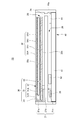
- FIG. 3 is a sectional view taken along line AA in FIG. 2.
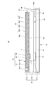
- FIG. 3 is a sectional view taken along line BB in FIG. 1 is an exploded perspective view showing a surface light emitter of a first embodiment according to the present invention.
- It is the expanded sectional view showing the part of one electrostatic sensor pattern of the sensor substrate of a 1st embodiment concerning the present invention.
- It is sectional drawing which shows the modification of the main-body part of 1st Embodiment which concerns on this invention.
- It is the front view which looked at the surface side of the sensor substrate mainly of 2nd Embodiment which concerns on this invention. It is sectional drawing of the main-body part of 2nd Embodiment which concerns on this invention.
- FIG. 1 is a front view showing an electrostatic sensor type switch with surface illumination 1 according to a first embodiment of the present invention
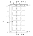
- FIG. 2 is a front view showing a main body 20 of the switch with surface illumination 1 according to the first embodiment. It is. 1 and 2 are front views of the side where the user brings the finger F closer to perform a switch operation.
- the surface located on the side closer to the finger F is referred to as “surface”.
- ”And the surface located on the opposite side of the front surface is referred to as“ back surface ”.
- the switch 1 with surface illumination is the top panel 10 (refer FIG. 1) arrange
- the top panel 10 has a display unit M that indicates an operation position with a figure, a character, or the like so that a position for performing each switch operation can be understood.
- this display part M is provided in the position corresponding to the electrostatic sensor pattern P (refer FIG. 2) formed in the sensor board
- the user looks at the display on the display unit M, and when the finger F is brought close to any position, the device for turning on / off the switch (for example, ceiling lighting or entrance door lighting) is turned on / off. It is possible to visually check whether the operation can be performed.
- the switch for example, ceiling lighting or entrance door lighting
- the top panel 10 includes a transparent or translucent plate located on the most surface side, and a film attached to the back surface of the plate, and the figure that becomes the display unit M on the film. And characters are printed.
- the film is configured such that at least a predetermined area on which graphics, characters, and the like are printed transmits light.
- a predetermined area where graphics, characters, etc. are printed is in a half mirror state. For this reason, when light is radiated from the main body 20 side when the surroundings are dark at night or the like, the formed figure, characters, etc. are displayed so as to emerge.
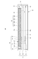
- FIG. 3 is a cross-sectional view taken along the line AA in FIG. 2
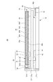
- FIG. 4 is a cross-sectional view taken along the line BB
- FIG. 5 is an exploded perspective view showing the surface light emitter 31.
- the main body 20 includes a housing 21, a light emitting member 30 having an electrostatic sensor pattern P (see FIG. 2), and a main control unit 40.
- casing 21 is provided with the frame part 21a used as a surrounding wall, the partition part 21b formed inside the frame part 21a, and the connection part 21c formed through the partition part 21b.
- the connection portion 21c is a portion that electrically connects a sensor substrate 33 and a control substrate 41, which will be described later, and in this embodiment, a connector-type connection portion 21c is formed integrally with the partition portion 21b by insert molding or the like.
- the connecting portion 21c is not limited to the connector type.
- the connection part 21c may be configured by a connection opening that penetrates the front and back of the partition part 21b, and an electrical wiring that electrically connects a sensor board 33 and a control board 41 described later through the connection opening.
- the frame portion 21a is provided with screw holes 22 through which screws formed so as to penetrate from the front surface side to the back surface side are provided at each of the four corners.
- the main body part 20 can be installed in the room wall. It has become.
- the top panel 10 is provided with an engaging portion that engages with the outer surface of the frame portion 21a on the back side of the plate, while the outer shape itself is a size that is slightly larger than the opening provided in the wall. It is attached to the housing 21 so as to cover the opening provided in the wall.
- the partition part 21b is formed so that it may be located in the intermediate position (in this example, a substantially center position) of the height of the frame part 21a in the front and back direction.
- casing 21 is provided with the surface side recessed part 25 of the surface side by which the light emitting member 30 is arrange
- the partition part 21b is provided along the portion of the short frame part 21a (see FIGS. 3 and 4) at a position on one end side where the light emitting member 30 is not disposed.
- a first opening 23 and a second opening 24 formed so as to penetrate the front and back sides are provided.
- the light emitting member 30 includes a surface light emitter 31 and a sensor substrate 33 attached to the surface light emitter 31 and having an electrostatic sensor pattern P (see FIG. 2) formed thereon.
- the surface light emitter 31 includes a light source 31 ⁇ / b> A (for example, an LED), a surface light emitting layer 32, and a case opened on the surface side that accommodates the light source 31 ⁇ / b> A and the surface light emitting layer 32.
- the case 31B does not have to be limited to a box-like one opened on the front side, and may be a frame-like one.
- the surface light emitting layer 32 and the light source 31A do not have to be integrated with each other by the case 31B.
- the surface light emitter 31 is disposed on the surface light emitting layer 32 so that the surface light emitting layer 32 emits light. What is necessary is just to provide the structure positioned so that light source 31A may be arrange
- the surface light emitting layer 32 is disposed on the back side of the light guide plate 32B where the light from the light source 31A is incident, and in order to efficiently radiate light guided in the light guide plate 32B from the surface of the light guide plate 32B.
- 32A for example, a reflection sheet or a reflection plate
- a light diffusion member a diffusion sheet 32C and a prism sheet
- the light diffusing member of the present embodiment includes the diffusion sheet 32C disposed on the surface of the light guide plate 32B and the prism sheet 32D disposed on the surface of the diffusion sheet 32C. Need not be limited to those using two sheets.
- the light source 31A is arranged such that the light emitting surface faces the side surface on the other end side of the light guide plate 32B, and the light source 31A is guided so that the surface side of the surface light emitter 31 can uniformly emit light.
- a plurality of optical plates 32B are provided along the side surface on the other end side.
- the sensor substrate 33 is arranged so that the portion where the electrostatic sensor pattern P is formed is located on the back surface side of the surface light emitter 31, and the back surface of the surface light emitter 31 (more specifically, the case 31B). And a surface 33a of the sensor substrate 33 are bonded with a double-sided tape.
- the attachment of the sensor substrate 33 to the surface light emitter 31 is not limited to being performed with a double-sided tape, and may be performed using an adhesive or the like.
- the portion where the electrostatic sensor pattern P is formed is positioned on the back side of the surface light emitter 31, the location itself where the sensor substrate 33 is attached to the surface light emitter 31 is the surface light emitter 31. It may be a side surface.
- the light emitting member 30 includes a flexible wiring board 34 that electrically connects the light source 31 ⁇ / b> A to a power supply pattern that supplies power to the light source 31 ⁇ / b> A formed on a part of the other end side of the sensor board 33, and the back surface of the sensor board 33. And an electrostatic sensor IC 35 attached to the side and electrically connected to the electrostatic sensor pattern P.
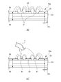
- FIG. 6 is an enlarged cross-sectional view showing a part of one electrostatic sensor pattern P of the sensor substrate 33.
- conductive patterns to be drive lines 51 and sensor lines 52 are formed on the surface 33 a of the sensor substrate 33.
- a conductive pattern serving as a ground 53 that is electrically connected to each other is formed on the front surface 33 a and the back surface 33 b of the sensor substrate 33.
- An electric field is generated between the drive line 51, the sensor line 52, and the ground 53.
- the state of the electric field is indicated by an arrow as a line of electric force.
- the electrostatic sensor IC 35 detects the decrease in the electric lines of force, that is, the change in the capacitance, thereby detecting whether or not the switch is operated.
- the configuration of the capacitance sensor is not necessarily limited to the configuration in which the electrostatic sensor pattern P as described above is configured and the capacitance change is detected by the electrostatic sensor IC 35.
- the configuration of the capacitance sensor is not necessarily limited to the configuration in which the electrostatic sensor pattern P as described above is configured and the capacitance change is detected by the electrostatic sensor IC 35.
- the finger F is away from the surface 33a of the sensor substrate 33, it can be detected only by the finger F being close. For this reason, even when the surface light emitter 31 and the top panel 10 are disposed on the surface 33a side of the sensor substrate 33, it is possible to detect well that the finger F has approached.
- the main control unit 40 is a part for performing overall control of the switch with surface illumination 1.
- the main control unit 40 is disposed in the back surface side concave portion 26 of the housing 21 so as to be separated from the light emitting member 30 and disposed on the back surface side of the surface light emitter 31 and provided on the sensor substrate 33 and the housing 21.
- the control board 41 electrically connected via the connection part 21c and the various electronic components attached to the control board 41 are provided.
- the main control unit 40 includes a control IC 42 attached to the control board 41, a wireless antenna 44 (see FIG. 4) attached to the surface of the control board 41 on the light emitting member 30 side, and the control board 41. And a human sensor 43 (see FIG. 3) attached to the surface on the light emitting member 30 side.
- a control board 41 for example, an electronic component for controlling power supplied from a power source accommodated in the switch box is also arranged.
- control board 41 is partially located on the outer side of the light emitting member 30 in a front view as viewed from the light emitting member 30 side.
- the human sensor 43 is placed on the control substrate 41 on one end side that is located outside the light emitting member 30 in a front view so as to be located immediately below the first opening 23 formed in the partition portion 21b of the housing 21. Is arranged.
- the wireless antenna 44 includes the light emitting member 30 such that the antenna portion 44 a of the wireless antenna 44 is positioned directly below the second opening 24 formed in the partition portion 21 b of the housing 21.
- a control board that is disposed at a position on the control board 41 on one end side that is located outside the light emitting member 30 in a front view as viewed from the side, and that a part of the wireless antenna 44 overlaps the light emitting member 30 in a front view. 41.
- the radio antenna 44 is large in size, it suffices that at least the antenna portion 44a is located at a position where it is not disturbed by the light emitting member 30 or the like. Therefore, as in the present embodiment, only the antenna portion 44a is positioned at a position that does not overlap with the light emitting member 30 in front view, and portions that do not have any problem in transmitting and receiving radio waves overlap with the light emitting member 30 in front view. Try to place it in position. According to this, from the viewpoint of the main body 20, the size of the control board 41 can be reduced, and the main body 20 can be downsized.
- any portion other than the antenna portion 44 a can be extended so as to overlap the wireless antenna 44 in a front view, so that a region for forming the electrostatic sensor pattern P can be widened. It becomes possible.
- the switch with surface illumination 1 configured as described above has a simple configuration with a small number of parts compared to a display device or the like having a touch panel function, manufacturing cost can be suppressed.
- each member the surface light emitter 31, the sensor substrate 33, the control substrate 41, etc.
- the thickness of the main body 20 can be reduced. For this reason, since the main-body part 20 can be attached so that it may not protrude from the opening formed in the wall of a room, it is possible to implement
- the sensor substrate 33 can be disposed close to the top panel 10, so that a change in capacitance is easily obtained and the finger F approaches. Can be detected well.
- the distance between the top panel 10 and the sensor substrate 33 can be stably maintained by attaching the sensor substrate 33 to the back surface of the surface light emitter 31, it is possible to suppress variations in capacitance due to variations in distance.
- the finger F can be detected accurately.
- the electrostatic sensor IC 35 is attached to the back side of the sensor substrate 33, and the light emitting member 30 includes the electrostatic sensor IC 35.
- the modification of the main body 20 illustrated in FIG. As described above, the electrostatic sensor IC 35 may be provided on the control board 41.
- control IC 42 electronic components other than the human sensor 43 and the wireless antenna 44 (for example, the control IC 42) may be provided on the back side of the control board 41.
- the control IC 42 electronic components other than the human sensor 43 and the wireless antenna 44
- the control board 41 may be provided on the front surface side of the control board 41.
- the thickness of the main control unit 40 can be reduced. It is preferable that all electronic components to be attached are provided on the surface side of the control board 41.
- FIG. 8 is a front view of the second embodiment as viewed mainly from the surface 33a side of the sensor substrate 33
- FIG. 9 is a cross-sectional view of the main body 20 of the second embodiment. 9 is a cross-sectional view at the same position as that shown in FIG.
- the sensor substrate 33 is a flexible substrate, and the same portion as the flexible wiring substrate 34 in the first embodiment is integrally formed on the sensor substrate 33.
- the light source 31 ⁇ / b> A is directly connected to the power supply pattern that supplies power to the light source 31 ⁇ / b> A formed on the sensor substrate 33.
- a corresponding bent portion X is provided on the other end side of the sensor substrate 33. Then, the light source 31A and the sensor substrate 33 are electrically connected in the same state as in the first embodiment (see FIG. 4) as shown in FIG. 9 by bending at the position of the two-dot chain line shown in the bent portion X. Can be connected.
- the sensor substrate 33 has a placement portion Y for placing the electrostatic sensor IC 35 provided on one of the long sides and extending outward.
- the electrostatic sensor IC 35 is attached to the surface side of the arrangement portion Y in a state before performing the operation.
- the arrangement portion Y is a surface light emitter of the sensor substrate 33.
- the electrostatic sensor IC 35 is folded back so that the electrostatic sensor IC 35 is located at a position opposite to the surface facing 31.
- the sensor substrate 33 of the second embodiment is configured to be approximately the same size as the outer size of the sensor substrate 33 of the first embodiment so that the arrangement portion Y does not protrude outside.
- the arrangement portion Y is fixed by sticking the back surface 33b of the arrangement portion Y before folding and the back surface 33b of the area where the electrostatic sensor pattern P is formed with a double-sided tape or the like. This fixing may be performed using an adhesive or the like.
- the sensor substrate 33 is arranged so that the portion where the electrostatic sensor pattern P is formed is located on the back side of the surface light emitter 31, and the surface light emitter 31.
- the back surface and the front surface 33a of the sensor substrate 33 are bonded with a double-sided tape, but the sensor substrate 33 may be bonded to the surface light emitter 31 using an adhesive or the like.
- the portion where the electrostatic sensor pattern P is formed is positioned on the back side of the surface light emitter 31, the portion itself where the sensor substrate 33 is attached to the surface light emitter 31 is the surface light emitter 31. It may be a side surface.
- the sensor substrate 33 by integrally forming the sensor substrate 33 with the same portion as the flexible wiring substrate 34 in the first embodiment, it is possible to further reduce the number of components and suppress the manufacturing cost.
- the non-flexible substrate has a thickness of about 0.3 mm
- the thickness of the flexible substrate is about 0.05 mm, which is about an order of magnitude thinner. Is easy to do.
- the electrostatic sensor IC 35 may be attached to the control board 41 side as shown in FIG.
- this invention is not limited to embodiment.
- the case where the light emitting member 30 is used for the switch with surface illumination 1 has been described, but the usage of the light emitting member 30 is not necessarily limited to the switch.
- switch with surface illumination was installed in the wall of a room
- the installation place of the switch 1 with surface illumination is not limited to the wall of a room
- switch with surface illumination 1 may be installed on furniture such as a desk, or may be installed in another location.
- SYMBOLS 1 Switch with surface illumination, 10 ... Top panel, 30 ... Light emitting member, 31 ... Surface light emitter, 31A ... Light source, 33 ... Sensor board, 34 ... Flexible wiring board, 35 ... Electrostatic sensor IC, 41 ... Control board, 42 ... Control IC, 43 ... Human sensor, 44 ... Wireless antenna, 44a ... Antenna part, P ... Electrostatic sensor pattern, F ... Finger
Landscapes
- Engineering & Computer Science (AREA)
- General Engineering & Computer Science (AREA)
- Switches That Are Operated By Magnetic Or Electric Fields (AREA)
- Arrangement Of Elements, Cooling, Sealing, Or The Like Of Lighting Devices (AREA)
- Planar Illumination Modules (AREA)
- Switch Cases, Indication, And Locking (AREA)
Abstract
スイッチ等に好適に用いることができる製造コストを低減した静電センサパターンを有する発光部材及びその発光部材を有する静電センサ型の面照明付スイッチを提供する。 本発明の発光部材(30)は、静電センサパターン(P)を有する発光部材(30)であって、光源(31A)を有する面発光体(31)と、面発光体(31)に貼り付けられ、静電センサパターン(P)が形成されたセンサ基板(33)と、を備え、センサ基板(33)は、静電センサパターン(P)が形成された部位が面発光体(31)の裏面側に位置するように配置されている。
Description
本発明は静電センサパターンを有する発光部材及びその発光部材を有する静電センサ型の面照明付スイッチに関する。
特許文献1には、タッチパネル機能を有する表示装置が開示されており、このような表示装置では、バックライトを備えているため、夜間等の暗いところでも操作性がよい。
しかしながら、上記のような表示装置は構成が複雑であり、製造コストが高いため、例えば、照明器具等の家電製品のON/OFFといった操作のために部屋等に設置されるスイッチ等に利用するには高価であるという問題がある。
本発明は、上記事情に鑑みてなされたものであり、スイッチ等に好適に用いることができる製造コストを低減した静電センサパターンを有する発光部材及びその発光部材を有する静電センサ型の面照明付スイッチを提供することを目的とする。
本発明は、上記目的を達成するために、以下の構成によって把握される。
(1)本発明の発光部材は、静電センサパターンを有する発光部材であって、光源を有する面発光体と、前記面発光体に貼り付けられ、静電センサパターンが形成されたセンサ基板と、を備え、前記センサ基板は、前記静電センサパターンが形成された部位が前記面発光体の裏面側に位置するように配置されている。
(1)本発明の発光部材は、静電センサパターンを有する発光部材であって、光源を有する面発光体と、前記面発光体に貼り付けられ、静電センサパターンが形成されたセンサ基板と、を備え、前記センサ基板は、前記静電センサパターンが形成された部位が前記面発光体の裏面側に位置するように配置されている。
(2)上記(1)の構成において、前記センサ基板には、前記光源に電力を供給する給電パターンが一部に形成されており、前記光源がフレキシブル配線基板で前記給電パターンに電気的に接続されている。
(3)上記(1)又は(2)の構成において、前記センサ基板に取り付けられ、前記静電センサパターンに電気的に接続された静電センサICを備えている。
(4)上記(1)の構成において、前記センサ基板は、前記光源に電力を供給する給電パターンが一部に形成されたフレキシブル基板であり、前記光源が前記給電パターンに直接接続されている。
(5)上記(4)の構成において、前記センサ基板に取り付けられ、前記静電センサパターンに電気的に接続された静電センサICを備えており、前記センサ基板は、外側に延在するように形成された前記静電センサICを配置する配置部を有し、前記静電センサICは、前記配置部の前記面発光体側に向く面上に取り付けられており、前記配置部は、前記センサ基板の前記面発光体を向く面の反対側の位置に前記静電センサICが位置するように折り返されている。
(6)本発明のスイッチは、静電センサ型の面照明付スイッチであって、上記(1)から(5)のいずれか1つの構成を有する発光部材と、前記発光部材から離間して前記面発光体の裏面側に配置され、前記センサ基板と電気的に接続された制御基板と、前記制御基板に取り付けられた制御ICと、前記制御基板の前記発光部材側の面に取り付けられた無線アンテナと、前記制御基板の前記発光部材側の面に取り付けられた人感センサと、を備え、前記制御基板は、前記発光部材側から見た正面視で、一部が前記発光部材よりも外側に位置し、前記人感センサは、前記正面視で前記発光部材よりも外側に位置する前記制御基板上に配置されており、前記無線アンテナは、前記無線アンテナのアンテナ部分が前記正面視で前記発光部材よりも外側に位置する前記制御基板上の位置に配置されているとともに、前記無線アンテナの一部が前記正面視で前記発光部材と重なる前記制御基板上の位置に配置されており、前記静電センサパターンがスイッチ操作のために指が近づけられる位置に対応した前記センサ基板上の位置に形成されている。
(7)本発明のスイッチは、静電センサ型の面照明付スイッチであって、上記(1)、(2)又は(4)のいずれか1つの構成を有する発光部材と、前記発光部材から離間して前記面発光体の裏面側に配置され、前記センサ基板と電気的に接続された制御基板と、前記制御基板に取り付けられた制御ICと、前記制御基板に取り付けられた静電センサICと、前記制御基板の前記発光部材側の面に取り付けられた無線アンテナと、前記制御基板の前記発光部材側の面に取り付けられた人感センサと、を備え、前記制御基板は、前記発光部材側から見た正面視で、一部が前記発光部材よりも外側に位置し、前記人感センサは、前記正面視で前記発光部材よりも外側に位置する前記制御基板上に配置されており、前記無線アンテナは、前記無線アンテナのアンテナ部分が前記正面視で前記発光部材よりも外側に位置する前記制御基板上の位置に配置されているとともに、前記無線アンテナの一部が前記正面視で前記発光部材と重なる前記制御基板上の位置に配置されており、前記静電センサパターンがスイッチ操作のために指が近づけられる位置に対応した前記センサ基板上の位置に形成されている。
(8)上記(6)又は(7)の構成において、前記発光部材の表面側に配置され、前記静電センサパターンに対応する位置に設けられた操作位置を示す表示部を有するトップパネルを備え、前記発光部材から放射される光が、少なくとも前記表示部を透過する。
(9)上記(8)の構成において、前記トップパネルは、前記表示部が印刷されたフィルムと、前記フィルムが貼り付けられたプレートと、を備えている。
本発明によれば、スイッチ等に好適に用いることができる製造コストを低減した静電センサパターンを有する発光部材及びその発光部材を有する静電センサ型の面照明付スイッチを提供することができる。
以下、本発明を実施するための形態(以下、「実施形態」という)を、添付図面に基づいて詳細に説明する。
なお、実施形態の説明の全体を通して同じ要素には同じ番号を付している。
なお、実施形態の説明の全体を通して同じ要素には同じ番号を付している。
(第1実施形態)
以下、本発明に係る第1実施形態の静電センサ型の面照明付スイッチ1について説明するとともに、その面照明付スイッチ1の説明に併せて、本発明に係る第1実施形態の静電センサパターンを有する発光部材30についても説明を行う。
以下、本発明に係る第1実施形態の静電センサ型の面照明付スイッチ1について説明するとともに、その面照明付スイッチ1の説明に併せて、本発明に係る第1実施形態の静電センサパターンを有する発光部材30についても説明を行う。
図1は本発明に係る第1実施形態の静電センサ型の面照明付スイッチ1を示す正面図であり、図2は第1実施形態の面照明付スイッチ1の本体部20を示す正面図である。
なお、図1及び図2は、ユーザがスイッチ操作を行うために指Fを近づける側を見た正面図になっており、以下の説明において、この指Fを近づける側に位置する面を「表面」と記載し、その表面の反対側に位置する面を「裏面」と記載する。
なお、図1及び図2は、ユーザがスイッチ操作を行うために指Fを近づける側を見た正面図になっており、以下の説明において、この指Fを近づける側に位置する面を「表面」と記載し、その表面の反対側に位置する面を「裏面」と記載する。
図1及び図2に示すように、面照明付スイッチ1は、最も表面側に配置されるトップパネル10(図1参照)と、そのトップパネル10の裏面側に配置される本体部20(図2参照)と、を備えている。
(トップパネル10)
図1に示すように、トップパネル10は、各スイッチ操作を行うための位置がわかるように、図形や文字等で操作位置を示す表示部Mを有している。
なお、この表示部Mは、面照明付スイッチ1の状態のときに、後述するセンサ基板33に形成されている静電センサパターンP(図2参照)に対応する位置に設けられている。
図1に示すように、トップパネル10は、各スイッチ操作を行うための位置がわかるように、図形や文字等で操作位置を示す表示部Mを有している。
なお、この表示部Mは、面照明付スイッチ1の状態のときに、後述するセンサ基板33に形成されている静電センサパターンP(図2参照)に対応する位置に設けられている。
したがって、ユーザは、表示部Mの表示を見ることで、どこの位置に指Fを近づければ、スイッチのON/OFFを行う機器(例えば、天井照明や玄関口照明等)のON/OFFの操作が行えるのかを視認することができるようになっている。
具体的には、トップパネル10は、最も表面側に位置する透明又は半透明のプレートと、そのプレートの裏面に貼り付けられたフィルムと、を備えており、そのフィルムに表示部Mとなる図形や文字等の印刷が行われている。
そして、フィルムは、少なくとも図形や文字等が印刷される所定のエリアが光を透過するようになっている。
そして、フィルムは、少なくとも図形や文字等が印刷される所定のエリアが光を透過するようになっている。
例えば、図形や文字等が印刷される所定のエリアについては、ハーフミラーの状態になっている。
このため、夜間等の周りが暗いときに、本体部20側から光が放射されると、その形成された図形や文字等が浮かび上がるように表示されるようになっている。
このため、夜間等の周りが暗いときに、本体部20側から光が放射されると、その形成された図形や文字等が浮かび上がるように表示されるようになっている。
一方、昼間等の周りが明るいときには、ハーフミラーによって光が反射されるため、描かれた図形や文字等がそのままユーザに視認される状態となり、フィルムよりも裏面側が透けて見えることがないため、見栄えが悪くなることがない。
(本体部20)
図3は図2のA-A線断面図であり、図4はB-B線断面図であり、図5は面発光体31を示す分解斜視図である。
図3及び図4に示すように、本体部20は、筐体21と、静電センサパターンP(図2参照)を有する発光部材30と、主制御部40と、を備えている。
図3は図2のA-A線断面図であり、図4はB-B線断面図であり、図5は面発光体31を示す分解斜視図である。
図3及び図4に示すように、本体部20は、筐体21と、静電センサパターンP(図2参照)を有する発光部材30と、主制御部40と、を備えている。
筐体21は、周壁となる枠部21aと、その枠部21aの内側に形成された仕切部21bと、仕切部21bを貫通して形成された接続部21cと、を備えている。
なお、接続部21cは、後述するセンサ基板33と制御基板41を電気的に接続する部分であり、本実施形態では、仕切部21bにインサート成形等でコネクタ型の接続部21cを一体に形成したものとしているが、接続部21cはコネクタ型であることに限定されるものではない。
例えば、接続部21cは、仕切部21bの表裏を貫通する接続開口と、その接続開口を通じて後述するセンサ基板33と制御基板41を電気的に接続する電気配線と、で構成されていてもよい。
なお、接続部21cは、後述するセンサ基板33と制御基板41を電気的に接続する部分であり、本実施形態では、仕切部21bにインサート成形等でコネクタ型の接続部21cを一体に形成したものとしているが、接続部21cはコネクタ型であることに限定されるものではない。
例えば、接続部21cは、仕切部21bの表裏を貫通する接続開口と、その接続開口を通じて後述するセンサ基板33と制御基板41を電気的に接続する電気配線と、で構成されていてもよい。
そして、枠部21aは、四隅のそれぞれに表面側から裏面側まで貫通するように形成されたネジを通すネジ孔22が設けられている。
したがって、例えば、部屋の壁に開口を設け、その開口の奥に設置されている既存のスイッチボックスに対して枠部21aをネジで固定することで、本体部20が部屋の壁に設置できるようになっている。
なお、トップパネル10は、プレートの裏面側に枠部21aの外面に係合する係合部が設けられている一方、外形自体は、この壁に設けられた開口よりも一回り大きい外形になっており、壁に設けられた開口を覆い隠すように、筐体21に取り付けられるようになっている。
また、仕切部21bは、枠部21aの表裏方向の高さの中間位置(本例では、ほぼ中央の位置)に位置するように形成されている。
このため、筐体21は、発光部材30が配置される表面側の表面側凹部25と、主制御部40が配置される裏面側の裏面側凹部26と、を備えるものになっている。
このため、筐体21は、発光部材30が配置される表面側の表面側凹部25と、主制御部40が配置される裏面側の裏面側凹部26と、を備えるものになっている。
さらに、仕切部21bは、図2に示すように、発光部材30が配置されていない一端側の位置に、幅の短い枠部21a(図3及び図4参照)の部分に沿って設けられ、表裏を貫通するように形成された第1開口部23及び第2開口部24を備えている。
(発光部材30)
発光部材30は、図3及び図4に示すように、面発光体31と、面発光体31に貼り付けられ、静電センサパターンP(図2参照)が形成されたセンサ基板33と、を備えている。
図3、図4及び図5に示すように、面発光体31は、光源31A(例えば、LED)と、面発光層32と、光源31A及び面発光層32を収容する表面側に開口したケース31Bと、を備えている。
なお、ケース31Bは、表面側に開口した箱状のものに限定される必要はなく、フレーム状のものであってもよい。
また、面発光体31は、ケース31Bによって面発光層32と光源31Aが一体にされている必要はなく、面発光体31は、面発光層32が発光するように面発光層32に対して光源31Aが配置されるように位置決めされる構成を備えていればよい。
発光部材30は、図3及び図4に示すように、面発光体31と、面発光体31に貼り付けられ、静電センサパターンP(図2参照)が形成されたセンサ基板33と、を備えている。
図3、図4及び図5に示すように、面発光体31は、光源31A(例えば、LED)と、面発光層32と、光源31A及び面発光層32を収容する表面側に開口したケース31Bと、を備えている。
なお、ケース31Bは、表面側に開口した箱状のものに限定される必要はなく、フレーム状のものであってもよい。
また、面発光体31は、ケース31Bによって面発光層32と光源31Aが一体にされている必要はなく、面発光体31は、面発光層32が発光するように面発光層32に対して光源31Aが配置されるように位置決めされる構成を備えていればよい。
面発光層32は、光源31Aからの光が入射する導光板32Bと、導光板32Bの裏面側に配置され、導光板32B内を導波する光を導光板32Bの表面から効率よく放射させるための反射部材32A(例えば、反射シート又は反射プレート)と、導光板32Bの表面から光が均一に放射されるように導光板32Bの表面側に配置される光拡散部材(拡散シート32C及びプリズムシート32D)と、を備えている。
本実施形態の光拡散部材は、導光板32Bの表面上に配置される拡散シート32Cと、拡散シート32Cの表面上に配置されるプリズムシート32Dと、を備えたものとしているが、光拡散部材は、2枚のシートを用いたものに限定される必要はない。
なお、図5に示すように、光源31Aは、発光面が導光板32Bの他端側の側面に対向するように配置され、面発光体31の表面側を均一に面発光できるように、導光板32Bの他端側の側面に沿って複数設けられている。
なお、図5に示すように、光源31Aは、発光面が導光板32Bの他端側の側面に対向するように配置され、面発光体31の表面側を均一に面発光できるように、導光板32Bの他端側の側面に沿って複数設けられている。
本実施形態では、静電センサパターンPが形成された部位が面発光体31の裏面側に位置するようにセンサ基板33が配置され、面発光体31(より具体的にはケース31B)の裏面とセンサ基板33の表面33aの間を両面テープで貼り合わすようにしている。
ただし、面発光体31へのセンサ基板33の貼り付けは、両面テープで行うことに限定される必要はなく、接着剤等を用いて貼り付けるようにしてもよい。
また、静電センサパターンPが形成された部位が面発光体31の裏面側に位置するようになっていれば、センサ基板33を面発光体31に貼り付ける箇所自体は、面発光体31の側面であってもよい。
また、静電センサパターンPが形成された部位が面発光体31の裏面側に位置するようになっていれば、センサ基板33を面発光体31に貼り付ける箇所自体は、面発光体31の側面であってもよい。
さらに、発光部材30は、センサ基板33の他端側の一部に形成された光源31Aに電力を供給する給電パターンに光源31Aを電気的に接続するフレキシブル配線基板34と、センサ基板33の裏面側に取り付けられ、静電センサパターンPに電気的に接続された静電センサIC35と、を備えている。
図6はセンサ基板33の1つの静電センサパターンPの部分を示した拡大断面図である。
図6(a)に示すように、センサ基板33の表面33aにはドライブライン51及びセンサーライン52となる導電パターンが形成されている。また、センサ基板33の表面33a及び裏面33bには、互いに電気的に接続されたグランド53となる導電パターンが形成されている。ドライブライン51とセンサーライン52及びグランド53との間に電界が生じている。図6(a)において、その電界の様子を電気力線として矢印で示している。
図6(a)に示すように、センサ基板33の表面33aにはドライブライン51及びセンサーライン52となる導電パターンが形成されている。また、センサ基板33の表面33a及び裏面33bには、互いに電気的に接続されたグランド53となる導電パターンが形成されている。ドライブライン51とセンサーライン52及びグランド53との間に電界が生じている。図6(a)において、その電界の様子を電気力線として矢印で示している。
図6(a)に示す状態のところに、図6(b)に示すように、人の指Fが近づくと電気力線が指F側に引っ張られ、センサーライン52への電気力線の本数が減少する。
この電気力線の減少、つまり、静電容量の変化を静電センサIC35が検知することで、スイッチの操作が行われたか否かを検出するようになっている。
この電気力線の減少、つまり、静電容量の変化を静電センサIC35が検知することで、スイッチの操作が行われたか否かを検出するようになっている。
静電容量センサの構成は、上記のような静電センサパターンPを構成し、静電容量の変化を静電センサIC35に検出させる構成のものに限定される必要はないが、本実施形態の電気力線の変化を検知する構成の場合、センサ基板33の表面33aから指Fが離れていても、指Fが近くにあるだけで検知することが可能である。
このため、センサ基板33の表面33a側に面発光体31やトップパネル10等が配置されている場合でも、指Fが近づいたことを良好に検知することが可能である。
このため、センサ基板33の表面33a側に面発光体31やトップパネル10等が配置されている場合でも、指Fが近づいたことを良好に検知することが可能である。
(主制御部40)
主制御部40は、面照明付スイッチ1の全体的な制御を行うための部分である。主制御部40は、筐体21の裏面側凹部26に配置されることで、発光部材30から離間して面発光体31の裏面側に配置され、センサ基板33と筐体21に設けられた接続部21cを介して電気的に接続された制御基板41と、その制御基板41に取り付けられた各種電子部品と、を備えている。
主制御部40は、面照明付スイッチ1の全体的な制御を行うための部分である。主制御部40は、筐体21の裏面側凹部26に配置されることで、発光部材30から離間して面発光体31の裏面側に配置され、センサ基板33と筐体21に設けられた接続部21cを介して電気的に接続された制御基板41と、その制御基板41に取り付けられた各種電子部品と、を備えている。
具体的には、主制御部40は、制御基板41に取り付けられた制御IC42と、制御基板41の発光部材30側の面に取り付けられた無線アンテナ44(図4参照)と、制御基板41の発光部材30側の面に取り付けられた人感センサ43(図3参照)と、を備えている。
なお、図示は省略しているが、制御基板41には、例えば、スイッチボックス内に収容された電源から供給される電力を制御するための電子部品等も配置される。
なお、図示は省略しているが、制御基板41には、例えば、スイッチボックス内に収容された電源から供給される電力を制御するための電子部品等も配置される。
そして、図3に示すように、制御基板41は、発光部材30側から見た正面視で、一端側の一部が発光部材30よりも外側に位置している。人感センサ43は、筐体21の仕切部21bに形成された第1開口部23の真下に位置するように、正面視で発光部材30よりも外側に位置する一端側の制御基板41上に配置されている。
また、図4に示すように、無線アンテナ44は、無線アンテナ44のアンテナ部分44aが、筐体21の仕切部21bに形成された第2開口部24の真下に位置するように、発光部材30側から見た正面視で、発光部材30よりも外側に位置する一端側の制御基板41上の位置に配置されているとともに、無線アンテナ44の一部が正面視で発光部材30と重なる制御基板41上の位置に配置されている。
無線アンテナ44は、サイズが大きいものの、少なくともアンテナ部分44aが発光部材30等に邪魔されない位置に位置していればよい。そこで、本実施形態のように、そのアンテナ部分44aだけを発光部材30と正面視で重ならない位置に位置させて、電波を送受信するのに問題ない部分については、発光部材30と正面視で重なる位置に配置するようにする。これによれば、本体部20としての視点で見れば、制御基板41のサイズを小さくすることができ、本体部20の小型化が可能となる。
また、発光部材30としての視点で見れば、アンテナ部分44a以外の部分であれば、無線アンテナ44に正面視で重なるように拡張できるため、静電センサパターンPを形成する領域を広く取ることが可能となる。
以上のような構成からなる面照明付スイッチ1は、タッチパネル機能を有する表示装置等と比べて、部品点数が少なくシンプルな構成であることから製造コストを抑制できる。
また、夜間等の周りが暗い時間帯等には、人感センサ43でユーザが近づいたことを検知して、発光部材30を発光させることができるため、タッチパネル機能を有する表示装置等と同様に、高い操作性を得ることができる。
さらに、各部材(面発光体31、センサ基板33及び制御基板41等)の厚みが薄いことから、本体部20の厚みを薄くすることが可能である。
このため、本体部20を部屋の壁に形成された開口から出っ張らないように取り付けることができるので、見栄えのよいスイッチを実現することが可能である。
このため、本体部20を部屋の壁に形成された開口から出っ張らないように取り付けることができるので、見栄えのよいスイッチを実現することが可能である。
加えて、面発光体31の厚みを薄くすることが可能となったことから、トップパネル10にセンサ基板33を近づけた配置とできるため、静電容量の変化が得られやすく、指Fが近づいたことを良好に検知することが可能である。
また、センサ基板33を面発光体31の裏面に張り付けたことにより、トップパネル10とセンサ基板33の距離を安定して保つことができるので、距離のばらつきに伴う静電容量のばらつきが抑制でき、正確な指Fの検知が可能である。
なお、上記では、センサ基板33の裏面側に静電センサIC35を取り付け、発光部材30が静電センサIC35を備えている場合で説明を行ったが、図7に示す本体部20の変形例のように、静電センサIC35が制御基板41に設けられていてもよい。
また、人感センサ43及び無線アンテナ44以外の電子部品(例えば、制御IC42等)は、制御基板41の裏面側に設けるようにしてもよい。
ただし、制御基板41に取り付けられる全ての電子部品を制御基板41の表面側に設けるようにしたほうが、主制御部40の厚さを薄くできるため、コンパクト化という視点に立てば、制御基板41に取り付けられる全ての電子部品が制御基板41の表面側に設けられていることが好ましい。
ただし、制御基板41に取り付けられる全ての電子部品を制御基板41の表面側に設けるようにしたほうが、主制御部40の厚さを薄くできるため、コンパクト化という視点に立てば、制御基板41に取り付けられる全ての電子部品が制御基板41の表面側に設けられていることが好ましい。
(第2実施形態)
次に、本発明に係る第2実施形態の静電センサ型の面照明付スイッチ1及び静電センサパターンPを有する発光部材30について説明する。
図8は第2実施形態の主にセンサ基板33の表面33a側を見た正面図であり、図9は第2実施形態の本体部20の断面図である。
なお、図9は図4で示したのと同様の位置の断面図になっている。
次に、本発明に係る第2実施形態の静電センサ型の面照明付スイッチ1及び静電センサパターンPを有する発光部材30について説明する。
図8は第2実施形態の主にセンサ基板33の表面33a側を見た正面図であり、図9は第2実施形態の本体部20の断面図である。
なお、図9は図4で示したのと同様の位置の断面図になっている。
第2実施形態は、発光部材30の構成の一部が第1実施形態と異なっているだけであるため、以下では、この異なる点について主に説明し、同様である部分については説明を省略する場合がある。
第2実施形態では、センサ基板33をフレキシブル基板として、第1実施形態におけるフレキシブル配線基板34と同様の部分をセンサ基板33に一体に形成したものとしている。
具体的には、図8に示すように、センサ基板33に形成されている光源31Aに電力を供給する給電パターンに光源31Aが直接接続されるように、第1実施形態におけるフレキシブル配線基板34に対応した折曲部Xをセンサ基板33の他端側に設けるようにしている。
そして、折曲部Xに示す二点鎖線の位置で折り曲げを行うことで、図9に示すように、第1実施形態と同様の状態(図4参照)で、光源31Aとセンサ基板33を電気的に接続することができる。
そして、折曲部Xに示す二点鎖線の位置で折り曲げを行うことで、図9に示すように、第1実施形態と同様の状態(図4参照)で、光源31Aとセンサ基板33を電気的に接続することができる。
また、図8に示すように、センサ基板33は、一方の長辺側に設けられ、外側に延在するように形成された静電センサIC35を配置する配置部Yを有しており、折り返しを行う前の状態で、配置部Yの表面側に静電センサIC35が取り付けられている。
そして、図8に示す二点鎖線の位置で配置部Yをセンサ基板33の静電センサパターンPが形成されている領域の裏面側に折り返す、つまり、配置部Yがセンサ基板33の面発光体31を向く面の反対側の位置に静電センサIC35が位置するように折り返される。これにより、第2実施形態のセンサ基板33は、外側に配置部Yが飛び出すことがないようにして、第1実施形態のセンサ基板33の外形サイズとほぼ同じサイズとなるようにされている。
なお、本実施形態では、折り返す前の配置部Yの裏面33bと静電センサパターンPが形成されている領域の裏面33bを両面テープ等で張り合わせることで、配置部Yを固定しているが、この固定は接着剤等を用いて行うようにしてもよい。
また、第1実施形態と同様に、本実施形態では、静電センサパターンPが形成された部位が面発光体31の裏面側に位置するようにセンサ基板33が配置され、面発光体31の裏面とセンサ基板33の表面33aの間を両面テープで貼り合わすようにしているが、面発光体31へのセンサ基板33の貼り付けは、接着剤等を用いて行ってもよい。
さらに、静電センサパターンPが形成された部位が面発光体31の裏面側に位置するようになっていれば、センサ基板33を面発光体31に貼り付ける箇所自体は、面発光体31の側面であってもよい。
このように、センサ基板33に第1実施形態におけるフレキシブル配線基板34と同様の部分を一体に形成するようにすることで、部品点数を更に減らし製造コストを抑制することが可能である。
また、フレキシブルでない基板が0.3mm程度の厚さを有しているのに対し、フレキシブル基板の厚さは0.05mm程度と一桁程度厚みが薄いため、より一層、本体部20の薄型化が行いやすい。
なお、第2実施形態においても、配置部Yを設けないようにして、図7に示したように、静電センサIC35が制御基板41側に取り付けられるようにしてもよい。
以上、本発明を実施形態に基づき説明したが、本発明は実施形態に限定されるものではない。
例えば、上記実施形態では、発光部材30が面照明付スイッチ1に用いられる場合について説明したが、発光部材30の使用用途はスイッチに限られる必要はない。
例えば、上記実施形態では、発光部材30が面照明付スイッチ1に用いられる場合について説明したが、発光部材30の使用用途はスイッチに限られる必要はない。
また、上記実施形態では、部屋の壁に面照明付スイッチ1を設置する場合で説明したが、面照明付スイッチ1の設置場所は、部屋の壁に限定されるものではなく、面照明付スイッチ1は机等の家具類に設置されてもよく、更に別の箇所に設置されてもよい。
このように本発明は、具体的な実施形態に限定されるものではなく、その要旨を逸脱しない範囲で種々変更が可能であり、そのことは当業者にとって請求の範囲の記載から明らかである。
1…面照明付スイッチ、10…トップパネル、30…発光部材、31…面発光体、31A…光源、33…センサ基板、34…フレキシブル配線基板、35…静電センサIC、41…制御基板、42…制御IC、43…人感センサ、44…無線アンテナ、44a…アンテナ部分、P…静電センサパターン、F…指
Claims (9)
- 静電センサパターンを有する発光部材であって、
光源を有する面発光体と、
前記面発光体に貼り付けられ、静電センサパターンが形成されたセンサ基板と、を備え、
前記センサ基板は、前記静電センサパターンが形成された部位が前記面発光体の裏面側に位置するように配置されていることを特徴とする発光部材。 - 前記センサ基板には、前記光源に電力を供給する給電パターンが一部に形成されており、
前記光源がフレキシブル配線基板で前記給電パターンに電気的に接続されていることを特徴とする請求項1に記載の発光部材。 - 前記センサ基板に取り付けられ、前記静電センサパターンに電気的に接続された静電センサICを備えていることを特徴とする請求項1又は請求項2に記載の発光部材。
- 前記センサ基板は、前記光源に電力を供給する給電パターンが一部に形成されたフレキシブル基板であり、
前記光源が前記給電パターンに直接接続されていることを特徴とする請求項1に記載の発光部材。 - 前記センサ基板に取り付けられ、前記静電センサパターンに電気的に接続された静電センサICを備えており、
前記センサ基板は、外側に延在するように形成された前記静電センサICを配置する配置部を有し、
前記静電センサICは、前記配置部の前記面発光体側に向く面上に取り付けられており、
前記配置部は、前記センサ基板の前記面発光体を向く面の反対側の位置に前記静電センサICが位置するように折り返されていることを特徴とする請求項4に記載の発光部材。 - 静電センサ型の面照明付スイッチであって、
請求項1から請求項5のいずれか1項に記載の発光部材と、
前記発光部材から離間して前記面発光体の裏面側に配置され、前記センサ基板と電気的に接続された制御基板と、
前記制御基板に取り付けられた制御ICと、
前記制御基板の前記発光部材側の面に取り付けられた無線アンテナと、
前記制御基板の前記発光部材側の面に取り付けられた人感センサと、を備え、
前記制御基板は、前記発光部材側から見た正面視で、一部が前記発光部材よりも外側に位置し、
前記人感センサは、前記正面視で前記発光部材よりも外側に位置する前記制御基板上に配置されており、
前記無線アンテナは、前記無線アンテナのアンテナ部分が前記正面視で前記発光部材よりも外側に位置する前記制御基板上の位置に配置されているとともに、前記無線アンテナの一部が前記正面視で前記発光部材と重なる前記制御基板上の位置に配置されており、
前記静電センサパターンがスイッチ操作のために指が近づけられる位置に対応した前記センサ基板上の位置に形成されていることを特徴とする面照明付スイッチ。 - 静電センサ型の面照明付スイッチであって、
請求項1、請求項2又は請求項4のいずれか1項に記載の発光部材と、
前記発光部材から離間して前記面発光体の裏面側に配置され、前記センサ基板と電気的に接続された制御基板と、
前記制御基板に取り付けられた制御ICと、
前記制御基板に取り付けられた静電センサICと、
前記制御基板の前記発光部材側の面に取り付けられた無線アンテナと、
前記制御基板の前記発光部材側の面に取り付けられた人感センサと、を備え、
前記制御基板は、前記発光部材側から見た正面視で、一部が前記発光部材よりも外側に位置し、
前記人感センサは、前記正面視で前記発光部材よりも外側に位置する前記制御基板上に配置されており、
前記無線アンテナは、前記無線アンテナのアンテナ部分が前記正面視で前記発光部材よりも外側に位置する前記制御基板上の位置に配置されているとともに、前記無線アンテナの一部が前記正面視で前記発光部材と重なる前記制御基板上の位置に配置されており、
前記静電センサパターンがスイッチ操作のために指が近づけられる位置に対応した前記センサ基板上の位置に形成されていることを特徴とする面照明付スイッチ。 - 前記発光部材の表面側に配置され、前記静電センサパターンに対応する位置に設けられた操作位置を示す表示部を有するトップパネルを備え、
前記発光部材から放射される光が、少なくとも前記表示部を透過することを特徴とする請求項6又は請求項7に記載の面照明付スイッチ。 - 前記トップパネルは、
前記表示部が印刷されたフィルムと、
前記フィルムが貼り付けられたプレートと、を備えていることを特徴とする請求項8に記載の面照明付スイッチ。
Applications Claiming Priority (2)
| Application Number | Priority Date | Filing Date | Title |
|---|---|---|---|
| JP2017013679A JP7001311B2 (ja) | 2017-01-27 | 2017-01-27 | 静電センサパターンを有する発光部材を有する静電センサ型の面照明付スイッチ |
| JP2017-013679 | 2017-01-27 |
Publications (1)
| Publication Number | Publication Date |
|---|---|
| WO2018139031A1 true WO2018139031A1 (ja) | 2018-08-02 |
Family
ID=62977966
Family Applications (1)
| Application Number | Title | Priority Date | Filing Date |
|---|---|---|---|
| PCT/JP2017/042432 Ceased WO2018139031A1 (ja) | 2017-01-27 | 2017-11-27 | 静電センサパターンを有する発光部材及びその発光部材を有する静電センサ型の面照明付スイッチ |
Country Status (2)
| Country | Link |
|---|---|
| JP (1) | JP7001311B2 (ja) |
| WO (1) | WO2018139031A1 (ja) |
Citations (5)
| Publication number | Priority date | Publication date | Assignee | Title |
|---|---|---|---|---|
| WO2012033207A1 (ja) * | 2010-09-10 | 2012-03-15 | 株式会社フジクラ | 照明モジュール |
| JP2012134030A (ja) * | 2010-12-22 | 2012-07-12 | Panasonic Corp | 多段スイッチ |
| JP2013093155A (ja) * | 2011-10-25 | 2013-05-16 | Tokai Rika Co Ltd | スイッチ装置 |
| JP2014107254A (ja) * | 2012-11-30 | 2014-06-09 | Alps Electric Co Ltd | 照光機能付き入力装置 |
| JP2016197497A (ja) * | 2015-04-02 | 2016-11-24 | 株式会社東海理化電機製作所 | 操作検出装置 |
-
2017
- 2017-01-27 JP JP2017013679A patent/JP7001311B2/ja active Active
- 2017-11-27 WO PCT/JP2017/042432 patent/WO2018139031A1/ja not_active Ceased
Patent Citations (5)
| Publication number | Priority date | Publication date | Assignee | Title |
|---|---|---|---|---|
| WO2012033207A1 (ja) * | 2010-09-10 | 2012-03-15 | 株式会社フジクラ | 照明モジュール |
| JP2012134030A (ja) * | 2010-12-22 | 2012-07-12 | Panasonic Corp | 多段スイッチ |
| JP2013093155A (ja) * | 2011-10-25 | 2013-05-16 | Tokai Rika Co Ltd | スイッチ装置 |
| JP2014107254A (ja) * | 2012-11-30 | 2014-06-09 | Alps Electric Co Ltd | 照光機能付き入力装置 |
| JP2016197497A (ja) * | 2015-04-02 | 2016-11-24 | 株式会社東海理化電機製作所 | 操作検出装置 |
Also Published As
| Publication number | Publication date |
|---|---|
| JP7001311B2 (ja) | 2022-02-03 |
| JP2018120838A (ja) | 2018-08-02 |
Similar Documents
| Publication | Publication Date | Title |
|---|---|---|
| US10355689B2 (en) | Touch switch unit and interior lighting apparatus for vehicle including the same | |
| EP3076071B1 (en) | Display apparatus | |
| JP2011028996A (ja) | Led光源ユニット、面状照明装置及び看板 | |
| JPWO2013038654A1 (ja) | 表示装置 | |
| KR20120007894A (ko) | 저장장치용 터치패널 | |
| JP2011096639A (ja) | バックライトタッチボタン | |
| CN112859443A (zh) | 显示装置 | |
| JP6954713B2 (ja) | 平面スイッチ | |
| JP7001311B2 (ja) | 静電センサパターンを有する発光部材を有する静電センサ型の面照明付スイッチ | |
| JP6453823B2 (ja) | 平面スイッチ | |
| JP5040819B2 (ja) | 電子機器及び電子部品 | |
| CN106484090B (zh) | 电子装置 | |
| US20170201253A1 (en) | Planar switch and planar switch unit | |
| JP6901200B2 (ja) | 取付板及びその取付板を備えた平面スイッチ | |
| TWI728462B (zh) | 觸控感測器、配線器具 | |
| CN217950028U (zh) | 导光结构与门锁 | |
| CN223987089U (zh) | 电容式触摸按键装置和医疗设备 | |
| JP2004134093A (ja) | 入力パネル装置 | |
| CN219809867U (zh) | 照明控制装置 | |
| JP2011154563A (ja) | キーボード装置及びこれを用いた電子機器 | |
| JP2020035156A (ja) | タッチパネル装置 | |
| JP2024147856A (ja) | 照明制御装置 | |
| JP6453828B2 (ja) | 平面スイッチ | |
| CN117824267A (zh) | 门体和具有该门体的制冷设备 | |
| CN119724876A (zh) | 具有发光图标的变压器 |
Legal Events
| Date | Code | Title | Description |
|---|---|---|---|
| 121 | Ep: the epo has been informed by wipo that ep was designated in this application |
Ref document number: 17893763 Country of ref document: EP Kind code of ref document: A1 |
|
| NENP | Non-entry into the national phase |
Ref country code: DE |
|
| 122 | Ep: pct application non-entry in european phase |
Ref document number: 17893763 Country of ref document: EP Kind code of ref document: A1 |