WO2018124115A1 - Surface treatment material and article fabricated using same - Google Patents
Surface treatment material and article fabricated using same Download PDFInfo
- Publication number
- WO2018124115A1 WO2018124115A1 PCT/JP2017/046749 JP2017046749W WO2018124115A1 WO 2018124115 A1 WO2018124115 A1 WO 2018124115A1 JP 2017046749 W JP2017046749 W JP 2017046749W WO 2018124115 A1 WO2018124115 A1 WO 2018124115A1
- Authority
- WO
- WIPO (PCT)
- Prior art keywords
- surface treatment
- conductive substrate
- metal
- treatment material
- material according
- Prior art date
Links
Images


Classifications
-
- C—CHEMISTRY; METALLURGY
- C25—ELECTROLYTIC OR ELECTROPHORETIC PROCESSES; APPARATUS THEREFOR
- C25D—PROCESSES FOR THE ELECTROLYTIC OR ELECTROPHORETIC PRODUCTION OF COATINGS; ELECTROFORMING; APPARATUS THEREFOR
- C25D3/00—Electroplating: Baths therefor
- C25D3/02—Electroplating: Baths therefor from solutions
- C25D3/12—Electroplating: Baths therefor from solutions of nickel or cobalt
-
- C—CHEMISTRY; METALLURGY
- C25—ELECTROLYTIC OR ELECTROPHORETIC PROCESSES; APPARATUS THEREFOR
- C25D—PROCESSES FOR THE ELECTROLYTIC OR ELECTROPHORETIC PRODUCTION OF COATINGS; ELECTROFORMING; APPARATUS THEREFOR
- C25D3/00—Electroplating: Baths therefor
- C25D3/02—Electroplating: Baths therefor from solutions
- C25D3/38—Electroplating: Baths therefor from solutions of copper
-
- C—CHEMISTRY; METALLURGY
- C25—ELECTROLYTIC OR ELECTROPHORETIC PROCESSES; APPARATUS THEREFOR
- C25D—PROCESSES FOR THE ELECTROLYTIC OR ELECTROPHORETIC PRODUCTION OF COATINGS; ELECTROFORMING; APPARATUS THEREFOR
- C25D5/00—Electroplating characterised by the process; Pretreatment or after-treatment of workpieces
- C25D5/10—Electroplating with more than one layer of the same or of different metals
- C25D5/12—Electroplating with more than one layer of the same or of different metals at least one layer being of nickel or chromium
-
- C—CHEMISTRY; METALLURGY
- C25—ELECTROLYTIC OR ELECTROPHORETIC PROCESSES; APPARATUS THEREFOR
- C25D—PROCESSES FOR THE ELECTROLYTIC OR ELECTROPHORETIC PRODUCTION OF COATINGS; ELECTROFORMING; APPARATUS THEREFOR
- C25D5/00—Electroplating characterised by the process; Pretreatment or after-treatment of workpieces
- C25D5/34—Pretreatment of metallic surfaces to be electroplated
- C25D5/42—Pretreatment of metallic surfaces to be electroplated of light metals
- C25D5/44—Aluminium
-
- C—CHEMISTRY; METALLURGY
- C25—ELECTROLYTIC OR ELECTROPHORETIC PROCESSES; APPARATUS THEREFOR
- C25D—PROCESSES FOR THE ELECTROLYTIC OR ELECTROPHORETIC PRODUCTION OF COATINGS; ELECTROFORMING; APPARATUS THEREFOR
- C25D5/00—Electroplating characterised by the process; Pretreatment or after-treatment of workpieces
- C25D5/60—Electroplating characterised by the structure or texture of the layers
- C25D5/615—Microstructure of the layers, e.g. mixed structure
- C25D5/617—Crystalline layers
-
- H—ELECTRICITY
- H01—ELECTRIC ELEMENTS
- H01B—CABLES; CONDUCTORS; INSULATORS; SELECTION OF MATERIALS FOR THEIR CONDUCTIVE, INSULATING OR DIELECTRIC PROPERTIES
- H01B1/00—Conductors or conductive bodies characterised by the conductive materials; Selection of materials as conductors
- H01B1/02—Conductors or conductive bodies characterised by the conductive materials; Selection of materials as conductors mainly consisting of metals or alloys
- H01B1/023—Alloys based on aluminium
-
- H—ELECTRICITY
- H01—ELECTRIC ELEMENTS
- H01R—ELECTRICALLY-CONDUCTIVE CONNECTIONS; STRUCTURAL ASSOCIATIONS OF A PLURALITY OF MUTUALLY-INSULATED ELECTRICAL CONNECTING ELEMENTS; COUPLING DEVICES; CURRENT COLLECTORS
- H01R13/00—Details of coupling devices of the kinds covered by groups H01R12/70 or H01R24/00 - H01R33/00
- H01R13/02—Contact members
- H01R13/03—Contact members characterised by the material, e.g. plating, or coating materials
-
- H—ELECTRICITY
- H01—ELECTRIC ELEMENTS
- H01R—ELECTRICALLY-CONDUCTIVE CONNECTIONS; STRUCTURAL ASSOCIATIONS OF A PLURALITY OF MUTUALLY-INSULATED ELECTRICAL CONNECTING ELEMENTS; COUPLING DEVICES; CURRENT COLLECTORS
- H01R43/00—Apparatus or processes specially adapted for manufacturing, assembling, maintaining, or repairing of line connectors or current collectors or for joining electric conductors
- H01R43/16—Apparatus or processes specially adapted for manufacturing, assembling, maintaining, or repairing of line connectors or current collectors or for joining electric conductors for manufacturing contact members, e.g. by punching and by bending
-
- C—CHEMISTRY; METALLURGY
- C23—COATING METALLIC MATERIAL; COATING MATERIAL WITH METALLIC MATERIAL; CHEMICAL SURFACE TREATMENT; DIFFUSION TREATMENT OF METALLIC MATERIAL; COATING BY VACUUM EVAPORATION, BY SPUTTERING, BY ION IMPLANTATION OR BY CHEMICAL VAPOUR DEPOSITION, IN GENERAL; INHIBITING CORROSION OF METALLIC MATERIAL OR INCRUSTATION IN GENERAL
- C23C—COATING METALLIC MATERIAL; COATING MATERIAL WITH METALLIC MATERIAL; SURFACE TREATMENT OF METALLIC MATERIAL BY DIFFUSION INTO THE SURFACE, BY CHEMICAL CONVERSION OR SUBSTITUTION; COATING BY VACUUM EVAPORATION, BY SPUTTERING, BY ION IMPLANTATION OR BY CHEMICAL VAPOUR DEPOSITION, IN GENERAL
- C23C18/00—Chemical coating by decomposition of either liquid compounds or solutions of the coating forming compounds, without leaving reaction products of surface material in the coating; Contact plating
- C23C18/16—Chemical coating by decomposition of either liquid compounds or solutions of the coating forming compounds, without leaving reaction products of surface material in the coating; Contact plating by reduction or substitution, e.g. electroless plating
- C23C18/1601—Process or apparatus
- C23C18/1633—Process of electroless plating
- C23C18/1646—Characteristics of the product obtained
- C23C18/165—Multilayered product
- C23C18/1653—Two or more layers with at least one layer obtained by electroless plating and one layer obtained by electroplating
-
- C—CHEMISTRY; METALLURGY
- C23—COATING METALLIC MATERIAL; COATING MATERIAL WITH METALLIC MATERIAL; CHEMICAL SURFACE TREATMENT; DIFFUSION TREATMENT OF METALLIC MATERIAL; COATING BY VACUUM EVAPORATION, BY SPUTTERING, BY ION IMPLANTATION OR BY CHEMICAL VAPOUR DEPOSITION, IN GENERAL; INHIBITING CORROSION OF METALLIC MATERIAL OR INCRUSTATION IN GENERAL
- C23C—COATING METALLIC MATERIAL; COATING MATERIAL WITH METALLIC MATERIAL; SURFACE TREATMENT OF METALLIC MATERIAL BY DIFFUSION INTO THE SURFACE, BY CHEMICAL CONVERSION OR SUBSTITUTION; COATING BY VACUUM EVAPORATION, BY SPUTTERING, BY ION IMPLANTATION OR BY CHEMICAL VAPOUR DEPOSITION, IN GENERAL
- C23C18/00—Chemical coating by decomposition of either liquid compounds or solutions of the coating forming compounds, without leaving reaction products of surface material in the coating; Contact plating
- C23C18/16—Chemical coating by decomposition of either liquid compounds or solutions of the coating forming compounds, without leaving reaction products of surface material in the coating; Contact plating by reduction or substitution, e.g. electroless plating
- C23C18/18—Pretreatment of the material to be coated
- C23C18/1803—Pretreatment of the material to be coated of metallic material surfaces or of a non-specific material surfaces
- C23C18/1824—Pretreatment of the material to be coated of metallic material surfaces or of a non-specific material surfaces by chemical pretreatment
- C23C18/1827—Pretreatment of the material to be coated of metallic material surfaces or of a non-specific material surfaces by chemical pretreatment only one step pretreatment
- C23C18/1831—Use of metal, e.g. activation, sensitisation with noble metals
-
- C—CHEMISTRY; METALLURGY
- C25—ELECTROLYTIC OR ELECTROPHORETIC PROCESSES; APPARATUS THEREFOR
- C25D—PROCESSES FOR THE ELECTROLYTIC OR ELECTROPHORETIC PRODUCTION OF COATINGS; ELECTROFORMING; APPARATUS THEREFOR
- C25D5/00—Electroplating characterised by the process; Pretreatment or after-treatment of workpieces
- C25D5/48—After-treatment of electroplated surfaces
- C25D5/50—After-treatment of electroplated surfaces by heat-treatment
Definitions
- the present invention relates to a surface treatment material and a part produced using the same, and particularly at least one layer on a conductive substrate that is mainly composed of a base metal having a high ionization tendency and is difficult to form a sound plating film.
- the present invention relates to a technique for easily and easily forming a surface treatment film comprising a metal layer with good adhesion.
- Copper, copper alloy, iron, iron alloy, etc. from the viewpoint of being inexpensive and relatively excellent in properties to be plated (conductive substrate) used for forming conventional electrical contacts, etc.
- the metal materials have been widely used. Such a metal material has particularly good conductivity and workability, is relatively easy to obtain, and can be easily coated on the surface, and has a surface with excellent plating adhesion. Therefore, it is still used as a mainstream material for conductive substrates.
- aluminum called light metal has a complicated surface plating method and it is difficult to form a plating film with good adhesion. This is because aluminum tends to form an oxide film called a passive film on its surface, and this oxide film exists in a stable state, and base metal such as aluminum is plated in a wet manner. It is difficult to do this.
- a base layer such as a nickel layer formed on the surface of an aluminum-based substrate for the purpose of improving plating adhesion, and a coating layer made of a metal (such as tin or silver) for electrical contact, for example,
- a metal such as tin or silver
- a zinc-containing solution called zincate treatment is performed using a zinc-containing solution, whereby the substrate and the plating film (the base layer and the coating layer) are formed.
- a pretreatment for increasing the adhesion strength was performed (for example, Patent Document 2).
- Patent Document 3 discloses an electronic component material in which an aluminum alloy is plated, and it was considered that a certain amount or more of a zinc layer is preferably present in order to obtain a sufficient bonding strength.
- plating may be performed without forming a zinc layer on the base material, but the manufacturing method is not specified. Therefore, the effect obtained when the zinc layer is reduced to the limit or when the zinc layer is not formed has not been studied.
- Patent Document 4 shows that a pre-treatment for forming fine etching recesses on the surface of the substrate by etching with an active acid treatment solution is performed, and the adhesion strength is enhanced by the anchor effect by the formed fine etching recesses. Yes.
- the unevenness such as 5-10 ⁇ m becomes a stress concentration point at the time of deformation, and there is a problem that bending workability deteriorates.
- a zinc layer formed with a thickness of, for example, about 100 nm is interposed between the substrate and the plating film, Since the main plating layer (plating film) is formed on this zinc layer, when heated, zinc in the zinc layer diffuses in the main plating layer, and further diffuses and appears to the surface layer of the main plating layer. As a result, various problems such as a problem of increasing the contact resistance, a decrease in wire bonding property, and a decrease in solder wettability are caused.
- a nickel-based plating layer is generally used, and it is mainly formed with the intention of improving adhesion and suppressing zinc diffusion in the zinc layer.
- the nickel-based plating layer is usually harder than the aluminum-based substrate, if the nickel-based plating layer is too thick in order to suppress the diffusion of zinc, it is bent in the process of manufacturing the terminals.
- the nickel-based plating layer (coating) cannot follow the deformation of the aluminum-based base material, cracks easily occur, and the corrosion resistance is inferior.
- JP 2014-63662 A JP 2014-47360 A JP 2012-087411 A JP 2002-115086 A JP 2011-99161 A
- an object of the present invention is to form a surface-treated film with good adhesion and easily in a short time on a conductive substrate that is mainly composed of a base metal having a particularly high ionization tendency and is difficult to form a sound plating film.
- Another object is to provide a surface treatment material that can be formed and also excellent in bending workability, and a component manufactured using the surface treatment material.
- the inventors of the present invention directly formed on the conductive substrate out of at least one metal layer constituting the surface treatment film formed on the conductive substrate. Pay attention to the bottom metal layer, which is the metal layer, and optimize the area ratio of the bottom metal layer that is in close contact (contact) with the conductive substrate within the predetermined observation area of the conductive substrate. As a result, it has been found that a surface treatment material excellent in both bending workability and adhesion properties can be provided, and the present invention has been achieved.
- the gist configuration of the present invention is as follows. (1) A surface treatment material having a conductive substrate and a surface treatment film composed of at least one metal layer formed on the conductive substrate, Of the at least one metal layer, the lowermost metal layer, which is a metal layer directly formed on the conductive substrate, is scattered on the conductive substrate and from the surface of the conductive substrate to the inside. Having a plurality of buried metal parts that branch out and extend, A first line segment drawn on the surface of the conductive substrate as viewed in a vertical cross section of the surface treatment material in which at least one metal embedded portion is present on the conductive substrate, and the metal embedded portion is the conductive material.
- the second line segment drawn through the end position that extends the longest along the thickness direction of the base and parallel to the first line segment, and the conductivity centered on the metal buried portion having the end position Observation of the conductive substrate in a region partitioned by third and fourth line segments passing through the position of the cross-sectional width of 20 ⁇ m of the substrate and orthogonal to the first line segment and the second line segment, respectively.
- a surface treatment material characterized in that, when the region is an area, the average value of the area ratio of the metal buried portion in the observation region is in the range of 5% to 50%.
- a surface treatment material having a conductive substrate and a surface treatment film composed of one or more metal layers on the conductive substrate Of the metal layers constituting the surface-treated film, the lowermost metal layer in contact with the conductive substrate has a plurality of metal embedded portions that branch out and extend from the surface of the conductive substrate toward the inside. And In a vertical cross section of the conductive substrate where the metal buried portion is present, expressed as (cross-sectional width 20 ⁇ m parallel to the surface of the conductive substrate) ⁇ (depth from the surface of the conductive substrate to the end position of the metal buried portion).
- the surface treatment material is characterized in that the average value of the area ratio of the metal buried portion in the observed region is in the range of 5% to 50%.
- the metal embedded portion has a maximum extension length of 0.5 ⁇ m or more and 25 ⁇ m or less when measured from the surface of the conductive substrate along the thickness direction to the end position.
- the surface treatment film includes the lowermost metal layer and one or more metal layers formed on the lowermost metal layer, and the one or more metal layers include nickel, a nickel alloy, Cobalt, cobalt alloy, copper, copper alloy, tin, tin alloy, silver, silver alloy, gold, gold alloy, platinum, platinum alloy, rhodium, rhodium alloy, ruthenium, ruthenium alloy, iridium, iridium alloy, palladium and palladium alloy.
- the surface treatment material according to any one of (1) to (5) above, wherein the surface treatment material is formed of any one selected from the group.
- the surface treatment material according to (6), wherein the one or more metal layers are composed of two or more metal layers.
- a conductive base which is mainly composed of a base metal having a high ionization tendency and is difficult to form a sound plating film, for example, aluminum or an aluminum alloy, and the conductive
- the lowermost metal layer has a plurality of metal buried portions that are scattered on the conductive substrate and extend from the surface of the conductive substrate so as to branch and extend.
- a surface treatment material having a conductive substrate and a surface treatment film composed of one or more metal layers on the conductive substrate, wherein the conductive material among the metal layers constituting the surface treatment film is conductive.
- the lowermost metal layer in contact with the conductive substrate has a plurality of metal buried portions that branch out and extend from the surface of the conductive substrate toward the inside.
- the metal buried part of the bottom metal layer penetrates into the inside of the conductive substrate, and as a result, a mechanical anchoring effect is obtained, and the manufacturing time is greatly increased.
- the first line segment drawn on the surface of the conductive substrate and the metal embedded portion are the thickness of the conductive substrate as viewed in a vertical cross section of the surface treatment material in which at least one metal embedded portion is present on the conductive substrate.
- the observation area When an area partitioned by the third and fourth line segments passing through the position and orthogonal to the first line segment and the second line segment is an observation area of the conductive substrate, the observation area
- the average value of the area ratio of the metal-buried portion is 5% or more and 50% or less. That is, in the vertical cross section of the conductive substrate where the metal burying portion exists, it is expressed by (cross-sectional width 20 ⁇ m parallel to the surface of the conductive substrate) ⁇ (depth from the surface of the conductive substrate to the end position of the metal burying portion).
- the average value of the area ratio of the metal buried portion in the observed region is in the range of 5% to 50%.
- the length of the first and second line segments is 20 ⁇ m
- the length of the third and fourth line segments is the depth from the surface of the conductive substrate to the end position of the metal buried portion in the thickness direction. is there. Therefore, the area of the observation region partitioned by the first to fourth line segments is (the cross-sectional width of 20 ⁇ m parallel to the surface of the conductive substrate) and (the depth from the surface of the conductive substrate to the terminal position of the metal buried portion). ( ⁇ m 2 ) multiplied by the area ( ⁇ m 2 ).
- the metal embedding portion of the lowermost metal layer penetrates into the inside of the conductive substrate, resulting in a mechanical anchoring effect.
- the metal buried portion of the lowermost metal layer branches and extends from the surface of the conductive substrate toward the inside, the branched portion is embedded more firmly inside the conductive substrate and is more excellent. It is possible to provide a surface treatment material exhibiting excellent adhesion.
- the area ratio of the metal buried portion that is in close contact (contact) with the conductive substrate is within a range of 5% to 50% within a predetermined observation region of the conductive substrate, It is possible to maintain the appropriate mechanical anchoring effect by allowing the metal in the metal embedded part to enter from any of the above, and as a result, to provide a surface treatment material excellent in both bending workability and adhesion properties Can do.
- Such a surface treatment material can maintain the original characteristics obtained after forming the surface treatment film without deteriorating even in a use environment at a high temperature (for example, about 200 ° C.), for example, Surface treatment material with high long-term reliability and various parts produced using the same, such as terminals, connectors, bus bars, lead frames, medical members, shield cases, coils, contact switches, cables, heat pipes, memory disks, etc. Offering is now possible.
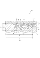
- FIG. 1 is a schematic cross-sectional view of a surface treatment material according to a first embodiment of the present invention.
- FIG. 2 is a view for explaining an observation region in the conductive base of the metal embedded portion formed on the surface treatment material according to the first embodiment and an area ratio of the metal embedded portion existing in the observation region.
- FIG. 3 is a schematic cross-sectional view of a surface treatment material according to the second embodiment.
- FIG. 4 is a SIM photograph when a cross section of a typical surface treatment material according to the present invention is observed.
- FIG. 1 is a schematic cross-sectional view of the surface treatment material of the first embodiment.
- the illustrated surface treatment material 10 includes a conductive substrate 1 and a surface treatment film 2.
- the conductive substrate 1 is not particularly limited.
- the conductive substrate 1 is mainly composed of a base metal having a high ionization tendency, and it is difficult to form a sound plating film using a wet plating method.
- Al or an aluminum alloy is preferable in that the effects of the present invention can be remarkably exhibited.
- the shape of the conductive substrate 1 is shown as an example in the drawing, it may be in the form of a plate, a wire, a bar, a tube, a foil, or the like, and can take various shapes depending on the application.
- the surface treatment film 2 is composed of at least one metal layer, in FIG. 1, one metal layer 3, and is formed on the conductive substrate 1.
- the surface treatment film 2 may be composed of one metal layer or may be composed of two or more metal layers, it is composed of one layer or two or more layers.
- the metal layer 3 (one layer) formed directly on the conductive substrate 1 is referred to as a “lowermost metal layer”. Since the surface treatment material 10 shown in FIG. 1 is composed of only one metal layer directly formed on the conductive substrate 1, the metal layer 3 is the lowermost metal layer.
- the lowermost metal layer 3 is not a zinc-containing layer formed by zincate treatment, but is a metal layer made of, for example, nickel (Ni), nickel alloy, cobalt (Co), cobalt alloy, copper (Cu), or copper alloy Is preferred.
- a suitable thickness of the lowermost metal layer 3 is 0.05 ⁇ m or more and 2.0 ⁇ m or less in consideration of solder wettability, contact resistance and bending workability after an environmental test at a high temperature (for example, 200 ° C.). Preferably, it is 0.1 ⁇ m or more and 1.5 ⁇ m or less, and more preferably 0.2 ⁇ m or more and 1.0 ⁇ m or less.
- the lowest metal layer is Ni
- good heat resistance is obtained
- Cu good
- good moldability is obtained.
- Ni or Co is used as the lowermost metal layer, there is an effect of reducing electrolytic corrosion of the aluminum base when the functional plating layer is damaged.
- the surface treatment film 2 includes a lowermost metal layer 3 and one or more metal layers 4 (for example, various functional plating layers) formed on the lowermost metal layer 3. It may be configured.
- the one or more metal layers 4 formed on the lowermost metal layer 3 for example, nickel (Ni), nickel alloy, cobalt (Co), cobalt alloy, copper (Cu), copper alloy, tin (Sn) , Tin alloy, silver (Ag), silver alloy, gold (Au), gold alloy, platinum (Pt), platinum alloy, rhodium (Rh), rhodium alloy, ruthenium (Ru), ruthenium alloy, iridium (Ir), iridium
- the alloys palladium (Pd), and palladium alloys, a metal or an alloy that is appropriately selected according to a desired property-imparting purpose can be given.
- nickel, a nickel alloy, cobalt, a cobalt alloy, copper, and the like are formed on the conductive substrate 1 that has been subjected to at least a surface activation process described later.
- the lowermost metal layer 3 made of a copper alloy is formed, and then, on the lowermost metal layer 3, as a coating layer for imparting the surface treatment material 10 with a function required for each component (bottommost) Nickel, nickel alloy, cobalt, cobalt alloy, copper, copper alloy, tin, tin alloy, silver, silver alloy, gold, gold alloy, platinum, platinum alloy, rhodium, rhodium alloy
- the metal layer 4 made of a metal or alloy selected from ruthenium, ruthenium alloy, iridium, iridium alloy, palladium and palladium alloy long-term confidence It can be obtained sex excellent surface treatment material (plating material) 10.
- the surface treatment film 2 is a metal having two or more layers including at least a lowermost metal layer 3 formed for the purpose of improving adhesion to the conductive substrate 1 and a metal layer 4 as a coating layer for imparting a function. It is preferable to consist of layers 3 and 4.
- a surface treatment film 2 can be formed by forming a plating layer on the lowermost metal layer 3, whereby a surface treatment material (plating material) 10 having excellent corrosion resistance can be provided.
- the method for forming the metal layers 3 and 4 is not particularly limited, but is preferably performed by a wet plating method.
- the characteristic configuration of the present invention is to control the area ratio of the lowermost metal layer 3 that is in close contact (contact) with the conductive substrate 1 in a predetermined observation region of the conductive substrate 1. More specifically, the lowermost metal layer 3 has a plurality of metal buried portions 3a that are scattered on the conductive substrate 1 and branch out and extend from the surface of the conductive substrate 1 to the inside.
- the average value of the area ratio of the metal-embedded portion 3a is within a range of 5% or more and 50% or less within a predetermined observation region of the conductive substrate 1, and is preferably within a range of 10% or more and 30% or less. The range of 15% or more and 25% or less is more preferable.
- the average value of the area ratio is less than 5%, the anchor effect is insufficient and sufficient adhesion cannot be obtained.
- the average value of the area ratio exceeds 50%, it is not preferable because it becomes a starting point of a crack in bending.
- the average value of the area ratio of the metal embedded portion 3a is in the range of 5% or more and 50% or less, the excellent adhesion between the conductive substrate 1 and the surface treatment film 2 can be obtained with the maximum anchor effect. It can be given in the state.
- the conductive substrate 1, in particular, the conductive substrate 1 which is a base metal having a large ionization tendency, for example, aluminum or an aluminum alloy, is generally subjected to a substitution treatment with zinc, that is, a so-called zincate treatment.
- the thickness of the zinc-containing layer existing between the conductive substrate and the surface treatment coating (plating coating) is, for example, about 100 nm, and zinc in this zinc-containing layer diffuses in the surface treatment coating.
- it may increase the contact resistance, and further deteriorate the wire bonding property, solder wettability, and corrosion resistance.
- the properties of the surface treatment material deteriorate due to use and long-term reliability is impaired.
- a zinc-containing layer does not exist between the conductive substrate 1 and the surface-treated film 2.
- the conductivity is increased. It has been considered difficult to form a surface-treated film (plating film) with good adhesion on the substrate 1, particularly the conductive substrate 1 which is a base metal having a large ionization tendency.
- the present inventors have conducted intensive studies, and as a result of performing a new surface activation treatment process on the surface of the conductive substrate 1 (for example, an aluminum substrate) prior to forming the surface treatment film 2. Since an oxide film stably present on the surface of the conductive substrate 1 can be effectively removed without forming a conventional zinc-containing layer (especially a zincate treatment layer), it is directly on the conductive substrate 1. Even if a surface treatment film (for example, nickel plating layer) is formed, the metal atom (for example, aluminum atom) constituting the conductive substrate 1 and the metal atom (for example, nickel atom) constituting the surface treatment film can be directly bonded, It has been found that the lowermost metal layer 3 can be easily formed with good adhesion to the conductive substrate 1.
- a surface treatment film for example, nickel plating layer
- the surface treatment material 10 of the present invention can form a surface treatment film having excellent adhesion without the presence of a zinc-containing layer. For example, it can be maintained without deterioration even in a use environment at about 200 ° C., and has excellent long-term reliability.
- the lowermost metal constituting the surface treatment film 2 is formed on the conductive substrate 1.
- the so-called “anchor effect” combined with the effect produced by effectively removing the oxide film stably present on the surface of the conductive substrate 1 described above.
- the adhesion of the surface treatment film 2 to the conductive substrate 1 can be remarkably improved. Although the mechanism by which such an effect occurs is not clear, it is likely that the oxide film present on the surface of the conductive substrate 1 is removed by performing a new surface activation treatment, so that the surface of the conductive substrate 1 is removed.
- the metal buried portion 3a of the lowermost metal layer 3 is preferentially directed from the surface of the conductive substrate 1 toward the inside through not only the boundary between the crystal and the crystal, which is mainly present, but also the crystal grain boundary. It is presumed that the above-mentioned effect can be expressed by creating a state in which it is easy to enter. Note that the structure in which the metal buried portion 3a of the lowermost metal layer 3 penetrates into the inside of the conductive substrate 1 as in the present invention is finely applied to the surface of the substrate by a method using zinc layer replacement used as a conventional technique or by etching.
- the surface treatment material of the present invention having such a configuration cannot be achieved by a method for forming a simple etching recess, and the adhesion is remarkably superior to the surface treatment material having a surface treatment film formed by a conventional method. ing. Furthermore, the method for producing the surface treatment material of the present invention is capable of producing the surface treatment material in a simple and short-time treatment without performing a complicated pretreatment process like the zincate treatment. In addition, it is possible to provide a surface treatment material (plating material) that is greatly improved from the viewpoint of production efficiency.
- the metal burying portion 3 a is a part of the lowermost metal layer 3, is scattered on the conductive base 1, and branches and extends from the surface of the conductive base 1 toward the inside. Therefore, the branched portion is more firmly embedded in the conductive substrate 1, and a surface treatment material with better adhesion can be provided.
- the observation area in the conductive substrate of the metal buried portion formed in the surface treatment material and the area ratio of the metal buried portion existing in the observation area will be described.
- a third line segment that passes through the position of the cross-sectional width of 20 ⁇ m of the conductive substrate 1 centering on the metal buried portion 3a having the terminal position F and is perpendicular to each of the first line segment L1 and the second line segment L2.
- a region partitioned by L3 and the fourth line segment L4 is defined as an observation region R of the conductive substrate 1 (a rectangular region surrounded by a broken line in FIG. 2).
- the maximum extension length L from the first line segment L1 to the terminal position F where the metal embedded portion 3a extends the longest along the thickness direction of the conductive substrate 1 is seen in the vertical section of the surface treatment material 10.
- the surface position (surface side base portion) S of the conductive substrate 1 to the terminal position F of the metal burying portion 3a penetrating the conductive substrate 1 in the thickness direction tx of the conductive substrate 1 It means the straight line length measured along.
- the maximum extension length L is formed by forming an arbitrary cross section of the surface treatment material 1 by, for example, cross-section polishing after resin filling, focused ion beam (FIB) processing, and cross-section forming methods such as ion milling and cross section polisher.
- the maximum extension length L is measured for the metal buried portion 3a existing in the observation region R.
- the maximum extension length L when measured from the surface of the conductive substrate to the end position F along the thickness direction is preferably 0.3 ⁇ m or more in order to improve adhesion, and is 0.5 ⁇ m or more and 25 ⁇ m or less. More preferably, it is the range. If the maximum extension length L of the metal-embedded portion 3a is less than 0.5 ⁇ m, the anchor effect cannot be sufficiently exhibited, and the effect of improving the adhesion may be small. In addition, when the average value of the maximum extension length L exceeds 25 ⁇ m, cracks occur in the surface treatment material 10, particularly the conductive substrate 1, when bending is performed with the metal embedded portion 3 a as the starting point. It is because it may become easy to do. In addition, when it is necessary to satisfy both adhesiveness and bending workability in a balanced manner, it is more preferable that the maximum extension length L be in the range of 2 ⁇ m to 10 ⁇ m.
- the cross-sectional width W of 20 ⁇ m is such that, after specifying the width end of the metal buried portion 3a having the terminal position F, the bisector of the width end width is defined as the center line C, and the conductive substrate with reference to the center line C. It means a cross-sectional width that is divided by 10 ⁇ m horizontally with respect to one plane direction.
- the observation area R means an area partitioned by a maximum extension length L and a cross-sectional width W of 20 ⁇ m.
- the average value of the area ratio of the metal buried portion 3 a penetrating into the inside of the conductive substrate 1 can be measured by observing the cross section of the surface treatment material 10.
- the area ratio of the metal embedded portion 3a existing in the observation region R is measured by calculating the area ratio of the metal embedded portion 3a using image analysis software such as Winroof.
- the area ratio of the metal burying portion 3a is measured at three arbitrary observation cross sections, and the average value of the three area ratios obtained is calculated.
- the metal embedding part 3a when the cross-section observation of the electroconductive base
- the extending shape of the metal embedded portion 3a that has penetrated into the crystal grain boundaries and the crystal grains is linear, curved, wedge-shaped, or the like. It is preferable to have a form that is continuously connected as a minute, and a form that penetrates into the inside of the conductive base material 1 by a number of line segment shapes such as a ant nest shape and a radial shape.
- the metal burying portion 3a when determining the extending shape of the metal burying portion 3a from the two-dimensional cross-sectional observation state, for example, when the metal burying portion 3a is observed in an enclave shape, further, a part of the metal burying portion 3a has a gap. Is observed as a metal buried portion 3a, and when a void is observed, the void portion is regarded as a part of the metal buried portion 3a, and the metal buried portion 3a The area ratio shall be measured.
- FIG. 4 shows a book having a metal-embedded portion 3a existing in an observation region R (rectangular region surrounded by a broken line in FIG. 4) divided by a cross-sectional width W having a maximum extension length L of 3.8 ⁇ m and 20 ⁇ m.
- the SIM photograph when the cross section of the surface treatment material of the invention is observed is shown as an example.
- the area ratio of the metal genus embedded portion 3a existing in the observation region R was 23%.
- aluminum for example, 1000 series aluminum such as A1100 defined by JIS H4000: 2014, and aluminum alloy (for example, defined by JIS H4000: 2014).
- 6000 Al—Mg—Si) -based alloy such as A6061)
- the electrolytic degreasing step is performed by, for example, immersing in an alkaline degreasing bath of 20 to 200 g / L sodium hydroxide (NaOH), using the substrate as a cathode, a current density of 2.5 to 5.0 A / dm 2 , and a bath temperature of 60.
- Examples of the method include cathodic electrolytic degreasing under the conditions of ° C and a processing time of 10 to 100 seconds.
- the surface activation treatment step is a novel activation treatment step different from the conventional activation treatment, and is the most important step among the steps for producing the surface treatment material of the present invention.
- a surface treatment film (plating) having good adhesion to the conductive substrate 1 which is a base metal having a particularly high ionization tendency. It was difficult to form a film.
- the present invention by performing the surface activation treatment step, oxidation that stably exists on the surface of the conductive substrate 1 without forming a zinc-containing layer mainly composed of zinc by zincate treatment or the like. The film can be effectively removed, and in addition, the same metal atom as the metal atom (for example, nickel atom) that constitutes the lowermost metal layer 3 directly formed on the conductive substrate 1 is then added to the lowermost metal.
- the layer 3 Before the layer 3 is formed, it can be formed on the conductive substrate 1 as a crystal nucleus or a thin layer. As a result, even if a surface treatment film (eg, nickel plating layer) is formed directly on the conductive substrate, metal atoms (eg, aluminum atoms) constituting the conductive substrate and metal atoms (eg, nickel) constituting the surface treatment film are formed. As a result of the direct bonding of the atoms), the surface-treated film 2 can be easily formed with good adhesion to the conductive substrate 1.
- a surface treatment film eg, nickel plating layer
- the surface of the conductive substrate 1 is subjected to (1) any acid solution 10 to 500 mL / L selected from sulfuric acid, nitric acid, hydrochloric acid, hydrofluoric acid and phosphoric acid, nickel sulfate, An activation treatment solution containing a nickel compound selected from the group consisting of nickel nitrate, nickel chloride and nickel sulfamate (0.1 to 500 g / L in terms of nickel metal content), (2) sulfuric acid and nitric acid 10 to 500 mL / L of an acid solution selected from hydrochloric acid, hydrofluoric acid and phosphoric acid, and a cobalt compound selected from the group consisting of cobalt sulfate, cobalt nitrate, cobalt chloride and cobalt sulfamate (cobalt (3) selected from sulfuric acid, nitric acid, hydrochloric acid, hydrofluoric acid, and phosphoric acid.
- a copper compound selected from the group consisting of copper sulfate, copper nitrate, copper chloride and copper sulfamate (0.1 to 500 g / L in terms of copper metal content).
- the treatment is preferably carried out by treatment, more preferably 200 to 400 seconds, still more preferably 250 to 300 seconds.
- a surface treatment film forming step is performed.
- the surface treatment film 2 may be formed only by the lowermost metal layer 3, but depending on the purpose of imparting characteristics (function) to the surface treatment material 10, Furthermore, one or more (other) metal layers 4 can be formed, and the surface treatment film 2 can be formed of at least two or more metal layers 3 and 4 including the lowermost metal layer 3.
- the lowermost metal layer 3 is formed by using a plating solution containing the same metal component as the main component metal in the activation treatment solution used in the surface activation treatment step, by a wet plating method of electrolytic plating or electroless plating. It can be carried out.
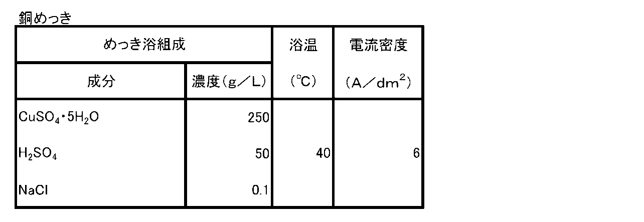
- Tables 1 to 3 exemplify plating bath compositions and plating conditions when the lowermost metal layer 3 is formed by nickel (Ni) plating, cobalt (Co) plating, and copper (Cu) plating, respectively.
- each metal layer 4 has characteristics (functions) in the surface treatment material.
- electroplating or electroless plating can be performed by a wet plating method.
- Tables 1 to 10 show nickel (Ni) plating, cobalt (Co) plating, copper (Cu) plating, tin (Sn) plating, silver (Ag) plating, silver (Ag) -tin (Sn) alloy plating, Examples of plating bath compositions and plating conditions when forming a metal layer by silver (Ag) -palladium (Pd) alloy plating, gold (Au) plating, palladium (Pd) plating, and rhodium (Rh) plating are illustrated.
- the surface treatment coating 2 has various layer configurations by appropriately combining the lowermost metal layer 3 as described above and one or more metal layers 4 formed on the lowermost metal layer 3 depending on the application. It is possible to change and form.
- the surface treatment material of the present invention is used for a lead frame, after forming a nickel plating layer as the lowermost metal layer 3 on the conductive substrate 1, silver plating on the lowermost metal layer 3,
- a metal layer (functional plating layer) composed of one or more kinds of plating selected from silver alloy plating, palladium plating, palladium alloy plating, gold plating, and gold alloy plating to form the surface treatment coating 2 Functions such as solder wettability, wire bonding property, and reflectance improvement can be imparted.
- the surface treatment material of this invention when using the surface treatment material of this invention by an electrical contact material, after forming a copper plating layer as the lowermost metal layer 3 on the electroconductive base
- the surface treatment material of the present invention is a base material such as a lighter aluminum or aluminum alloy instead of a conventionally used base material such as iron, iron alloy, copper, copper alloy as a base material (conductive base).
- Materials can be used, terminals, connectors, bus bars, lead frames, medical members (eg catheter guide wires, stents, artificial joints, etc.), shield cases (eg for electromagnetic wave prevention), coils (eg for motors), accessories (For example, necklaces, earrings, rings, etc.), contact switches, cables (for example, aircraft wire harnesses), heat pipes, memory disks, and other various parts (products) can be applied.
- the surface activation of the base material is enabled without the conventional thick zinc-containing layer of about 100 nm (particularly the zincate treatment layer) existing between the base material and the surface treatment film.
- the product group consisting of iron, iron alloy, copper, and copper alloy, and it is especially necessary to reduce the weight of automobile wire harnesses, aerospace cases, and electromagnetic shielding cases. It can be used in various products.
- the surface activation treatment is carried out by using 10 to 500 mL / L of any acid solution selected from sulfuric acid, nitric acid, hydrochloric acid, hydrofluoric acid and phosphoric acid, nickel sulfate, Using an activation treatment liquid containing a nickel compound selected from the group consisting of nickel nitrate, nickel chloride and nickel sulfamate (0.1 to 500 g / L in terms of nickel metal content), a treatment temperature of 20 It is performed under the conditions of treatment at ⁇ 60 ° C., current density of 0.1 ⁇ 20 A / dm 2 and treatment time of 200 ⁇ 900 seconds.
- Cobalt selected from the group consisting of 10 to 500 mL / L of any selected acid solution and cobalt sulfate, cobalt nitrate, cobalt chloride and cobalt sulfamate Compound (in terms of metal content of cobalt 0.1 ⁇ 500g / L) using the activation solution containing a processing temperature 20 ⁇ 60 ° C., a current density of 0.1 ⁇ 20 A / dm 2 and processing It is carried out under the conditions of treatment at a time of 200 to 900 seconds.
- any acid solution selected from sulfuric acid, nitric acid, hydrochloric acid, hydrofluoric acid and phosphoric acid is 10 to 500 mL /
- the surface treatment film 2 composed of the lowermost metal layer 3 and the surface plating layer which is the metal layer 4 formed on the lowermost metal layer 3 is formed.
- the surface treatment material 10 of the invention was produced.
- Kind of base material (conductive base 1), kind of metal compound contained in activation treatment liquid used for surface activation treatment, maximum extension length L and area ratio of metal embedding part 3a, and bottom metal layer 3 and the thickness of the metal layer 4 are shown in Table 11. Further, the formation conditions of the metal layers 3 and 4 constituting the surface treatment film 2 were performed according to the plating conditions shown in Tables 1 to 10.
- Conventional Example 1 performs an electrolytic degreasing process on the aluminum base material (size 0.2 mm ⁇ 30 mm ⁇ 30 mm) shown in Table 11 under the above-described conditions, and then performs a conventional zinc replacement process (zincate process). A zinc-containing layer having a thickness of 110 nm was formed. Then, without performing surface activation treatment, a surface treatment film composed of two metal layers consisting of a nickel plating layer and a gold plating layer is formed at the thickness shown in Table 11 by the surface treatment film formation step described above. Then, a surface treatment material was produced.
- Conventional Example 2 refers to an example of Patent Document 4 in which a surface treatment film is produced by simulating a surface treatment film on a substrate.
- a surface treatment film is produced by simulating a surface treatment film on a substrate.
- the aluminum base material size 0.2 mm ⁇ 30 mm ⁇ 30 mm shown in Table 11
- an electrolytic degreasing process is performed under the above-described conditions, and then the aluminum base material is sunlite which is an active acid solution mainly composed of hydrochloric acid.
- Aluminum pre-treated by etching by dipping “NAS-727” (mainly 18% hydrochloric acid), manufactured and sold by the company, in an etching solution diluted twice, at a temperature of 35 ° C. for 2 minutes.
- a substrate was prepared.
- the surface of the pretreated aluminum substrate was subjected to a surface activation treatment.
- the surface activation treatment is a group consisting of 10 to 500 mL / L of any acid solution selected from sulfuric acid, nitric acid, hydrochloric acid, hydrofluoric acid and phosphoric acid, and nickel sulfate, nickel nitrate, nickel chloride and nickel sulfamate.
- the treatment was performed under the conditions of dm 2 and a treatment time of 1 to 50 seconds.
- a surface treatment film composed of two metal layers composed of a nickel plating layer and a gold plating layer is formed with the thickness shown in Table 11, A surface treatment material was prepared.
- Comparative Example 1 the surface activation treatment is carried out with 10 to 500 mL / L of any acid solution selected from sulfuric acid, nitric acid, hydrochloric acid, hydrofluoric acid and phosphoric acid, nickel sulfate, nickel nitrate, nickel chloride and sulfamine.
- An activation treatment solution containing a nickel compound selected from the group consisting of nickel oxide (0.1 to 500 g / L in terms of nickel metal content) is used, a treatment temperature of 20 to 60 ° C., a current density of 0.
- the treatment was performed under the conditions of treatment at 05 A / dm 2 and a treatment time of 0.5 seconds. Since the surface treatment material produced in Comparative Example 1 had a low current density and a short treatment time, no metal buried portion was present in the lowermost metal layer.
- the bending workability is determined by performing a V-bending test at a bending radius of 0.5 mm in a direction perpendicular to the rolling rebar (rolling direction).
- Table 12 shows the results of surface observation of the top of the top with a microscope (VHX200; manufactured by Keyence Corporation) at an observation magnification of 200 times.
- the bending workability shown in Table 12 is “ ⁇ (excellent)” when no cracks are observed on the surface of the top, and “ ⁇ (good)” when wrinkles are generated but not cracks.
- “ ⁇ (possible)”, “ ⁇ (possible)”, and “ ⁇ (impossible)” when the relatively large crack occurred Cases corresponding to “Good” and “Fair” were evaluated as having acceptable bending workability.
- Solder wettability is determined by subjecting each test material (surface treatment material) to a state in which the surface treatment film is formed (as it is plated) (unheated state) and a heat treatment in air at 200 ° C. for 24 hours. 2 types of samples (state after heat treatment) were prepared, and the solder wetting time was measured using a solder checker (SAT-5100 (trade name, manufactured by Reska Co., Ltd.)) and evaluated from this measured value. did. Table 12 shows the evaluation results. In addition, the solder wettability shown in Table 12 is as follows when the measurement condition details are as follows.
- solder wet time is less than 3 seconds, it is determined as “ ⁇ (excellent) ”, and when it is 3 seconds or more and less than 5 seconds Is judged as “ ⁇ (good)”, the case where it is 5 seconds or more and less than 10 seconds is judged as “ ⁇ (possible)”, and the case where it is not joined even after being immersed for 10 seconds is judged as “ ⁇ (impossible)”
- the cases corresponding to “ ⁇ (excellent)”, “ ⁇ (good)”, and “ ⁇ (possible)” were evaluated as having acceptable solder wettability.
- Solder type Sn-3Ag-0.5Cu Temperature: 250 ° C
- Test piece size 10 mm x 30 mm
- Flux isopropyl alcohol-25% rosin immersion speed: 25 mm / sec.
- Immersion time 10 seconds
- Immersion depth 10 mm
- a conductive substrate which is mainly composed of a base metal having a high ionization tendency and is difficult to form a sound plating film, for example, aluminum or an aluminum alloy, and the conductive material.
- the process is simplified compared to a conventional surface treatment material in which a zinc-containing layer (particularly a zincate treatment layer) having a thickness of about 100 nm is interposed.
- a zinc-containing layer particularly a zincate treatment layer
- the metal buried portion of the lowermost metal layer penetrates into the inside of the conductive substrate, and as a result, the mechanical anchoring effect is obtained.
- the manufacturing time can be greatly shortened.
- Surface treatment material can be provided.
- the original characteristics obtained after the surface treatment film is formed can be maintained without deterioration even under a use environment at a high temperature (for example, about 200 ° C.), and the surface has high long-term reliability.
- Treatment materials and various parts (products) manufactured using them such as terminals, connectors, bus bars, lead frames, medical materials, shield cases, coils, contact switches, cables, heat pipes, memory disks, etc., can be provided Became.
Abstract
Description
さらに、ドローンやウエアラブルデバイスでは、雨や汗がデバイス内部に入り込む可能性があり、長期信頼性を確保するためにも、高い耐食性が求められる。風力発電のような塩水環境における変圧器のモータやインバータも同様である。しかしながら、亜鉛置換処理後に形成されるめっき層(下地層)を薄く形成すると、不均一なめっき層の形成やピンホールの形成により、亜鉛含有層を完全に被覆することは困難であり、塩水環境において亜鉛含有層に沿って侵食が優先的に進行し、その結果、下地層と基材の間において剥離が生じてしまうという問題がある。このため、上述したような問題が生じないようにするためにも、基体とめっき被膜との間には、亜鉛層が存在しないことが望ましく、また、亜鉛層の形成が必要な場合には、できるだけ厚さを薄くした亜鉛層を形成することが望まれていた。 Moreover, depending on the formation state of the zinc layer in the zincate treatment, there are cases in which plating defects such as bumps in the subsequent main plating and abnormal deposition occur frequently.
Furthermore, drones and wearable devices may have rain and sweat inside the device, and high corrosion resistance is required to ensure long-term reliability. The same applies to transformer motors and inverters in salt water environments such as wind power generation. However, if the plating layer (underlayer) formed after the zinc replacement treatment is thinly formed, it is difficult to completely cover the zinc-containing layer due to the formation of a non-uniform plating layer or pinholes. In this case, erosion preferentially proceeds along the zinc-containing layer, and as a result, there is a problem that peeling occurs between the underlayer and the base material. For this reason, in order to prevent the above-described problems from occurring, it is desirable that there is no zinc layer between the substrate and the plating film, and when formation of the zinc layer is necessary, It has been desired to form a zinc layer that is as thin as possible.
(1)導電性基体と、該導電性基体上に形成された少なくとも1層以上の金属層からなる表面処理被膜とを有する表面処理材であって、
前記少なくとも1層以上の金属層のうち、前記導電性基体上に直接形成されている金属層である最下金属層が、前記導電性基体に点在しかつ前記導電性基体の表面から内部に向かって枝分かれして広がって延在する複数の金属埋設部を有し、
前記導電性基体に前記金属埋設部が少なくとも1つ存在する前記表面処理材の垂直断面で見て、前記導電性基体の表面に引いた第1の線分と、前記金属埋設部が前記導電性基体の厚さ方向に沿って最も長く延在する終端位置を通り前記第1の線分と平行に引いた第2の線分と、前記終端位置をもつ金属埋設部を中心とする前記導電性基体の断面幅20μmの位置を通り、かつ前記第1の線分と前記第2の線分のそれぞれと直交する第3及び第4の線分とで区画した領域を、前記導電性基体の観察領域とするとき、該観察領域に占める前記金属埋設部の面積割合の平均値が、5%以上50%以下の範囲であることを特徴とする表面処理材。
(2)導電性基体と、該導電性基体上に1層以上の金属層からなる表面処理被膜と、を有する表面処理材であって、
前記表面処理被膜を構成する金属層のうち、前記導電性基体に接する最下金属層が、前記導電性基体の表面から内部に向かって枝分かれして広がって延在する複数の金属埋設部を有し、
前記金属埋設部が存在する前記導電性基体の垂直断面において、(導電性基体の表面に平行な断面幅20μm)×(導電性基体の表面から金属埋設部の終端位置までの深さ)で表される観察領域に占める前記金属埋設部の面積割合の平均値が、5%以上50%以下の範囲であることを特徴とする表面処理材。
(3)前記金属埋設部は、前記導電性基体の表面から厚さ方向に沿って前記終端位置まで測定したときの最大延在長さが0.5μm以上25μm以下の範囲であることを特徴とする、上記(1)または(2)に記載の表面処理材。
(4)前記導電性基体は、アルミニウム、またはアルミニウム合金であることを特徴とする、上記(1)乃至(3)のいずれか1つに記載の表面処理材。
(5)前記最下金属層は、ニッケル、ニッケル合金、コバルト、コバルト合金、銅または銅合金であることを特徴とする、 上記(1)乃至(4)のいずれか1つに記載の表面処理材。
(6)前記表面処理被膜は、前記最下金属層と、該最下金属層上に形成された1層以上の金属層とからなり、該1層以上の金属層が、ニッケル、ニッケル合金、コバルト、コバルト合金、銅、銅合金、錫、錫合金、銀、銀合金、金、金合金、白金、白金合金、ロジウム、ロジウム合金、ルテニウム、ルテニウム合金、イリジウム、イリジウム合金、パラジウムおよびパラジウム合金の群から選択されるいずれかで形成されたものであることを特徴とする、上記(1)乃至(5)のいずれか1つに記載の表面処理材。
(7)前記1層以上の金属層が、2層以上の金属層からなることを特徴とする、上記(6)に記載の表面処理材。
(8)上記(1)乃至(7)のいずれか1つに記載の表面処理材を用いて作製された端子。
(9)上記(1)乃至(7)のいずれか1つに記載の表面処理材を用いて作製されたコネクタ。
(10)上記(1)乃至(7)のいずれか1つに記載の表面処理材を用いて作製されたバスバー。
(11)上記(1)乃至(7)のいずれか1つに記載の表面処理材を用いて作製されたリードフレーム。
(12)上記(1)乃至(7)のいずれか1つに記載の表面処理材を用いて作製された医療部材。
(13)上記(1)乃至(7)のいずれか1つに記載の表面処理材を用いて作製されたシールドケース。
(14)上記(1)乃至(7)のいずれか1つに記載の表面処理材を用いて作製されたコイル。
(15)上記(1)乃至(7)のいずれか1つに記載の表面処理材を用いて作製されたコンタクトスイッチ。
(16)上記(1)乃至(7)のいずれか1つに記載の表面処理材を用いて作製されたケーブル。
(17)上記(1)乃至(7)のいずれか1つに記載の表面処理材を用いて作製されたヒートパイプ。
(18)上記(1)乃至(7)のいずれか1つに記載の表面処理材を用いて作製されたメモリーディスク。 That is, the gist configuration of the present invention is as follows.
(1) A surface treatment material having a conductive substrate and a surface treatment film composed of at least one metal layer formed on the conductive substrate,
Of the at least one metal layer, the lowermost metal layer, which is a metal layer directly formed on the conductive substrate, is scattered on the conductive substrate and from the surface of the conductive substrate to the inside. Having a plurality of buried metal parts that branch out and extend,
A first line segment drawn on the surface of the conductive substrate as viewed in a vertical cross section of the surface treatment material in which at least one metal embedded portion is present on the conductive substrate, and the metal embedded portion is the conductive material. The second line segment drawn through the end position that extends the longest along the thickness direction of the base and parallel to the first line segment, and the conductivity centered on the metal buried portion having the end position Observation of the conductive substrate in a region partitioned by third and fourth line segments passing through the position of the cross-sectional width of 20 μm of the substrate and orthogonal to the first line segment and the second line segment, respectively. A surface treatment material characterized in that, when the region is an area, the average value of the area ratio of the metal buried portion in the observation region is in the range of 5% to 50%.
(2) A surface treatment material having a conductive substrate and a surface treatment film composed of one or more metal layers on the conductive substrate,
Of the metal layers constituting the surface-treated film, the lowermost metal layer in contact with the conductive substrate has a plurality of metal embedded portions that branch out and extend from the surface of the conductive substrate toward the inside. And
In a vertical cross section of the conductive substrate where the metal buried portion is present, expressed as (cross-sectional width 20 μm parallel to the surface of the conductive substrate) × (depth from the surface of the conductive substrate to the end position of the metal buried portion). The surface treatment material is characterized in that the average value of the area ratio of the metal buried portion in the observed region is in the range of 5% to 50%.
(3) The metal embedded portion has a maximum extension length of 0.5 μm or more and 25 μm or less when measured from the surface of the conductive substrate along the thickness direction to the end position. The surface treatment material according to (1) or (2) above.
(4) The surface treatment material according to any one of (1) to (3), wherein the conductive substrate is aluminum or an aluminum alloy.
(5) The surface treatment according to any one of (1) to (4), wherein the lowermost metal layer is nickel, nickel alloy, cobalt, cobalt alloy, copper, or copper alloy. Wood.
(6) The surface treatment film includes the lowermost metal layer and one or more metal layers formed on the lowermost metal layer, and the one or more metal layers include nickel, a nickel alloy, Cobalt, cobalt alloy, copper, copper alloy, tin, tin alloy, silver, silver alloy, gold, gold alloy, platinum, platinum alloy, rhodium, rhodium alloy, ruthenium, ruthenium alloy, iridium, iridium alloy, palladium and palladium alloy The surface treatment material according to any one of (1) to (5) above, wherein the surface treatment material is formed of any one selected from the group.
(7) The surface treatment material according to (6), wherein the one or more metal layers are composed of two or more metal layers.
(8) A terminal manufactured using the surface treatment material according to any one of (1) to (7) above.
(9) A connector manufactured using the surface treatment material according to any one of (1) to (7) above.
(10) A bus bar produced using the surface treatment material according to any one of (1) to (7) above.
(11) A lead frame manufactured using the surface treatment material according to any one of (1) to (7) above.
(12) A medical member produced using the surface treatment material according to any one of (1) to (7) above.
(13) A shield case produced using the surface treatment material according to any one of (1) to (7) above.
(14) A coil manufactured using the surface treatment material according to any one of (1) to (7) above.
(15) A contact switch manufactured using the surface treatment material according to any one of (1) to (7) above.
(16) A cable manufactured using the surface treatment material according to any one of (1) to (7) above.
(17) A heat pipe produced using the surface treatment material according to any one of (1) to (7) above.
(18) A memory disk manufactured using the surface treatment material according to any one of (1) to (7) above.
また、導電性基体に金属埋設部が少なくとも1つ存在する表面処理材の垂直断面で見て、導電性基体の表面に引いた第1の線分と、金属埋設部が前記導電性基体の厚さ方向に沿って最も長く延在する終端位置を通り第1の線分と平行に引いた第2の線分と、終端位置をもつ金属埋設部を中心とする導電性基体の断面幅20μmの位置を通り、かつ前記第1の線分と前記第2の線分のそれぞれと直交する第3及び第4の線分とで区画した領域を、導電性基体の観察領域とするとき、観察領域に占める前記金属埋設部の面積割合の平均値が5%以上50%以下の範囲である。すなわち、金属埋設部が存在する導電性基体の垂直断面において、(導電性基体の表面に平行な断面幅20μm)×(導電性基体の表面から金属埋設部の終端位置までの深さ)で表される観察領域に占める金属埋設部の面積割合の平均値が、5%以上50%以下の範囲である。第1及び第2の線分の長さは20μmであり、第3及び第4の線分の長さは導電性基体の表面からその厚さ方向に金属埋設部の終端位置までの深さである。従って、第1から第4の線分で区画された観察領域の面積は、(導電性基体の表面に平行な断面幅20μm)と(導電性基体の表面から金属埋設部の終端位置までの深さ(μm))を乗じた面積(μm2)で表される。
本発明では上記のような特徴を有することによって、最下金属層の金属埋設部が、導電性基体の内部にまで侵入することにより機械的投錨効果が得られる結果、良好な密着性を示し、さらに製造時間も大幅に短縮することができる表面処理材を提供できるようになる。また、最下金属層の金属埋設部が、導電性基体の表面から内部に向かって枝分かれして広がって延在するため、枝分かれした部分が導電性基体の内部でより強固に埋め込まれ、より優れた密着性を示す表面処理材を提供することができる。また、導電性基体に密着(接触)する金属埋設部の面積割合が、導電性基体の所定の観察領域内で、5%以上50%以下の範囲であることにより、結晶粒界および結晶粒内のいずれからも金属埋設部の金属を侵入させて、適正な機械的投錨効果を維持することができ、その結果、曲げ加工性と密着性の双方の特性に優れた表面処理材を提供することができる。このような表面処理材は、表面処理被膜を形成した後に得られる本来の特性を、例えば高温(例えば200℃程度)での使用環境下であっても劣化させずに維持することができるため、長期信頼性が高い表面処理材およびこれを用いて作製される種々の部品、例えば端子、コネクタ、バスバー、リードフレーム、医療部材、シールドケース、コイル、コンタクトスイッチ、ケーブル、ヒートパイプ、メモリーディスク等の提供が可能になった。 According to the present invention, a conductive base, which is mainly composed of a base metal having a high ionization tendency and is difficult to form a sound plating film, for example, aluminum or an aluminum alloy, and the conductive A surface treatment material having a surface treatment film composed of at least one or more metal layers formed on a substrate, and among the at least one or more metal layers, a metal layer directly formed on a conductive substrate The lowermost metal layer has a plurality of metal buried portions that are scattered on the conductive substrate and extend from the surface of the conductive substrate so as to branch and extend. According to the present invention, there is also provided a surface treatment material having a conductive substrate and a surface treatment film composed of one or more metal layers on the conductive substrate, wherein the conductive material among the metal layers constituting the surface treatment film is conductive. The lowermost metal layer in contact with the conductive substrate has a plurality of metal buried portions that branch out and extend from the surface of the conductive substrate toward the inside. As a result, the process is simplified as compared with the conventional surface treatment material in which a zinc-containing layer (particularly a zincate treatment layer) having a thickness of, for example, about 100 nm is interposed between the substrate and the plating film. In addition, the metal buried part of the bottom metal layer penetrates into the inside of the conductive substrate, and as a result, a mechanical anchoring effect is obtained, and the manufacturing time is greatly increased. Thus, it becomes possible to provide a surface treatment material that can be shortened.
In addition, the first line segment drawn on the surface of the conductive substrate and the metal embedded portion are the thickness of the conductive substrate as viewed in a vertical cross section of the surface treatment material in which at least one metal embedded portion is present on the conductive substrate. A second line segment that passes through the end position that extends the longest along the vertical direction and is drawn in parallel with the first line segment, and a cross-sectional width of 20 μm of the conductive substrate centering on the metal buried portion having the end position. When an area partitioned by the third and fourth line segments passing through the position and orthogonal to the first line segment and the second line segment is an observation area of the conductive substrate, the observation area The average value of the area ratio of the metal-buried portion is 5% or more and 50% or less. That is, in the vertical cross section of the conductive substrate where the metal burying portion exists, it is expressed by (cross-sectional width 20 μm parallel to the surface of the conductive substrate) × (depth from the surface of the conductive substrate to the end position of the metal burying portion). The average value of the area ratio of the metal buried portion in the observed region is in the range of 5% to 50%. The length of the first and second line segments is 20 μm, and the length of the third and fourth line segments is the depth from the surface of the conductive substrate to the end position of the metal buried portion in the thickness direction. is there. Therefore, the area of the observation region partitioned by the first to fourth line segments is (the cross-sectional width of 20 μm parallel to the surface of the conductive substrate) and (the depth from the surface of the conductive substrate to the terminal position of the metal buried portion). (Μm 2 ) multiplied by the area (μm 2 ).
In the present invention, by having the above-described characteristics, the metal embedding portion of the lowermost metal layer penetrates into the inside of the conductive substrate, resulting in a mechanical anchoring effect. Furthermore, it becomes possible to provide a surface treatment material that can greatly reduce the manufacturing time. In addition, since the metal buried portion of the lowermost metal layer branches and extends from the surface of the conductive substrate toward the inside, the branched portion is embedded more firmly inside the conductive substrate and is more excellent. It is possible to provide a surface treatment material exhibiting excellent adhesion. Further, when the area ratio of the metal buried portion that is in close contact (contact) with the conductive substrate is within a range of 5% to 50% within a predetermined observation region of the conductive substrate, It is possible to maintain the appropriate mechanical anchoring effect by allowing the metal in the metal embedded part to enter from any of the above, and as a result, to provide a surface treatment material excellent in both bending workability and adhesion properties Can do. Since such a surface treatment material can maintain the original characteristics obtained after forming the surface treatment film without deteriorating even in a use environment at a high temperature (for example, about 200 ° C.), for example, Surface treatment material with high long-term reliability and various parts produced using the same, such as terminals, connectors, bus bars, lead frames, medical members, shield cases, coils, contact switches, cables, heat pipes, memory disks, etc. Offering is now possible.
導電性基体1は、特に限定するものではないが、例えばイオン化傾向が大きい卑な金属で主として構成され、なかでも湿式めっき法を用いて健全なめっき被膜の形成が難しいとされる、例えばアルミニウム(Al)またはアルミニウム合金であることが、本発明の効果を顕著に奏することができる点で好ましい。さらに、導電性基体1の形状は、図面においては条での例を示しているが、板、線、棒、管、箔などの形態でもよく、用途によって様々な形状を採ることができる。 (Conductive substrate)
The
表面処理被膜2は、少なくとも1層以上の金属層、図1では1層の金属層3で構成され、導電性基体1上に形成されている。ここで、表面処理被膜2は、1層の金属層で構成される場合と2層以上の金属層で構成される場合があるため、1層で構成される場合および2層以上で構成される場合のいずれにおいても、本発明では、導電性基体1上に直接形成されている(1層の)金属層3を、「最下金属層」と呼称することとする。なお、図1に示す表面処理材10は、導電性基体1上に直接形成されている金属層の1層のみで構成されているため、この金属層3は最下金属層である。 (Surface treatment film)
The
本発明の特徴的な構成は、最下金属層3の、導電性基体1に密着(接触)する部分が、導電性基体1の所定の観察領域内に占める面積割合を制御することにある。より具体的には、最下金属層3が、導電性基体1に点在しかつ導電性基体1の表面から内部に向かって枝分かれして広がって延在する複数の金属埋設部3aを有し、金属埋設部3aの面積割合の平均値が、導電性基体1の所定の観察領域内で、5%以上50%以下の範囲内であることにあり、10%以上30%以下の範囲が好ましく、15%以上25%以下の範囲がより好ましい。面積割合の平均値が5%未満であるとアンカー効果が不十分であり、密着性が十分に得られない。一方で、面積割合の平均値が50%を超えてしまうと、曲げ加工の際にクラックの起点となってしまうため好ましくない。金属埋設部3aの面積割合の平均値が、5%以上50%以下の範囲内であることにより、導電性基体1と表面処理被膜2との優れた密着性を、アンカー効果を最大限出現させた状態で付与することができる。 (Characteristic configuration of the present invention)
The characteristic configuration of the present invention is to control the area ratio of the
次に、本発明に従う表面処理材の製造方法におけるいくつかの実施形態を以下で説明する。 (Surface treatment material manufacturing method)
Next, some embodiments of the method for producing a surface treatment material according to the present invention will be described below.
電解脱脂工程は、例えば20~200g/Lの水酸化ナトリウム(NaOH)のアルカリ脱脂浴中に浸漬し、前記基材を陰極とし、電流密度2.5~5.0A/dm2、浴温60℃、処理時間10~100秒の条件で陰極電解脱脂する方法が挙げられる。 (Electrolytic degreasing process)
The electrolytic degreasing step is performed by, for example, immersing in an alkaline degreasing bath of 20 to 200 g / L sodium hydroxide (NaOH), using the substrate as a cathode, a current density of 2.5 to 5.0 A / dm 2 , and a bath temperature of 60. Examples of the method include cathodic electrolytic degreasing under the conditions of ° C and a processing time of 10 to 100 seconds.
電解脱脂工程を行った後に、表面活性化処理工程を行う。表面活性化処理工程は、従来の活性化処理とは異なる新規な活性化処理工程であって、本発明の表面処理材を製造する工程の中で最も重要な工程である。 (Surface activation treatment process)
After performing the electrolytic degreasing process, the surface activation process is performed. The surface activation treatment step is a novel activation treatment step different from the conventional activation treatment, and is the most important step among the steps for producing the surface treatment material of the present invention.
表面活性化処理工程を行った後に、表面処理被膜形成工程を行う。表面処理被膜形成工程は、最下金属層3だけで表面処理被膜2を形成してもよいが、表面処理材10に特性(機能)を付与する目的に応じて、最下金属層3上にさらに1層以上の(他の)金属層4を形成して、最下金属層3を含む少なくとも2層以上の金属層3、4で表面処理被膜2を形成することができる。 (Surface treatment film formation process)
After performing the surface activation treatment step, a surface treatment film forming step is performed. In the surface treatment film forming step, the
最下金属層3の形成は、表面活性化処理工程で用いた活性化処理液中の主成分金属と同一の金属成分を含有するめっき液を用い、電解めっきまたは無電解めっきの湿式めっき法によって行うことができる。表1~表3に、それぞれニッケル(Ni)めっき、コバルト(Co)めっきおよび銅(Cu)めっき、により最下金属層3を形成する際のめっき浴組成およびめっき条件を例示する。 (Bottom metal layer formation process)
The


表面処理被膜2を構成する金属層3、4のうち、最下金属層3以外の(他の)金属層4を形成する場合には、各金属層4は、表面処理材に特性(機能)を付与する目的に応じて、電解めっきまたは無電解めっきの湿式めっき法によって行うことができる。表1~表10に、それぞれニッケル(Ni)めっき、コバルト(Co)めっき、銅(Cu)めっき、錫(Sn)めっき、銀(Ag)めっき、銀(Ag)-錫(Sn)合金めっき、銀(Ag)-パラジウム(Pd)合金めっき、金(Au)めっき、パラジウム(Pd)めっきおよびロジウム(Rh)めっきにより金属層を形成する際のめっき浴組成およびめっき条件を例示する。 (Metal layer formation process other than the bottom metal layer)
When (other)


発明例1~36は、表11に示すアルミニウム系基材(サイズ0.2mm×30mm×30mm)上に、上述した条件で電解脱脂工程を行い、その後、導電性基体1の表面に、表面活性化処理を施した。表面活性化処理は、発明例1~16および19~21においては、硫酸、硝酸、塩酸、フッ酸およびリン酸の中から選択されるいずれかの酸溶液10~500mL/Lと、硫酸ニッケル、硝酸ニッケル、塩化ニッケルおよびスルファミン酸ニッケルからなる群から選択されるニッケル化合物(ニッケルのメタル分に換算して0.1~500g/L)とを含有する活性化処理液を使用し、処理温度20~60℃、電流密度0.1~20A/dm2および処理時間200~900秒にて処理する条件で行い、また、発明例17では、硫酸、硝酸、塩酸、フッ酸およびリン酸の中から選択されるいずれかの酸溶液10~500mL/Lと、硫酸コバルト、硝酸コバルト、塩化コバルトおよびスルファミン酸コバルトからなる群から選択されるコバルト化合物(コバルトのメタル分に換算して0.1~500g/L)とを含有する活性化処理液を使用し、処理温度20~60℃、電流密度0.1~20 A/dm2および処理時間200~900秒にて処理する条件で行い、さらに、発明例18および22~36では、硫酸、硝酸、塩酸、フッ酸およびリン酸の中から選択されるいずれかの酸溶液10~500mL/Lと、硫酸銅、硝酸銅、塩化銅およびスルファミン酸銅からなる群から選択される銅化合物(銅のメタル分に換算して0.1~500g/L)とを含有する活性化処理液を使用し、処理温度20~60℃、電流密度0.1~20A/dm2および処理時間200~900秒にて処理する条件で行った。その後、上述した表面処理被膜形成工程によって、最下金属層3と、最下金属層3上に形成された金属層4である表層めっき層とで構成された表面処理被膜2を形成し、本発明の表面処理材10を作製した。基材(導電性基体1)の種類、表面活性化処理に用いる活性化処理液中に含有させる金属化合物の種類、金属埋設部3aの最大延在長さLおよび面積割合、ならびに最下金属層3および金属層4の厚さについては、表11に示す。また、表面処理被膜2を構成する各金属層3、4の形成条件については、表1~表10に示すめっき条件により行った。 (Invention Examples 1-36)
Inventive Examples 1 to 36 were subjected to an electrolytic degreasing process on the aluminum base material (size 0.2 mm × 30 mm × 30 mm) shown in Table 11 under the above-described conditions, and then the surface of the
従来例1は、表11に示すアルミニウム基材(サイズ0.2mm×30mm×30mm)上に、上述した条件で電解脱脂工程を行い、その後、従来の亜鉛置換処理(ジンケート処理)を行うことによって、厚さ110nmの亜鉛含有層を形成した。その後、表面活性化処理を行うことなく、上述した表面処理被膜形成工程によって、表11に示す厚さでニッケルめっき層と金めっき層からなる2層の金属層で構成される表面処理被膜を形成し、表面処理材を作製した。 (Conventional example 1)
Conventional Example 1 performs an electrolytic degreasing process on the aluminum base material (size 0.2 mm × 30 mm × 30 mm) shown in Table 11 under the above-described conditions, and then performs a conventional zinc replacement process (zincate process). A zinc-containing layer having a thickness of 110 nm was formed. Then, without performing surface activation treatment, a surface treatment film composed of two metal layers consisting of a nickel plating layer and a gold plating layer is formed at the thickness shown in Table 11 by the surface treatment film formation step described above. Then, a surface treatment material was produced.
従来例2は、特許文献4の実施例を参照して、基材上に表面処理被膜を模擬して形成し、表面処理材を作製したものである。表11に示すアルミニウム基材(サイズ0.2mm×30mm×30mm)上に、上述した条件で電解脱脂工程を行い、その後、アルミニウム基材を、塩酸を主成分とする活性酸液であるサンライト株式会社によって製造販売されている「NAS-727」(18%塩酸が主成分)を2倍に薄めたエッチング溶液中に35°Cの温度で2分間浸漬して、エッチング処理により前処理したアルミニウム基材を作製した。その後、前処理したアルミニウム基体の表面に、表面活性化処理を施した。表面活性化処理は、硫酸、硝酸、塩酸、フッ酸およびリン酸の中から選択されるいずれかの酸溶液10~500mL/Lと、硫酸ニッケル、硝酸ニッケル、塩化ニッケルおよびスルファミン酸ニッケルからなる群から選択されるニッケル化合物(ニッケルのメタル分に換算して0.1~500g/L)とを含有する活性化処理液を使用し、処理温度20~60℃、電流密度0.1~20A/dm2および処理時間1~50秒にて処理する条件で行った。表面活性化処理を行った後に、上述した表面処理被膜形成工程によって、表11に示す厚さでニッケルめっき層と金めっき層からなる2層の金属層で構成される表面処理被膜を形成し、表面処理材を作製した。 (Conventional example 2)
Conventional Example 2 refers to an example of
比較例1は、表面活性化処理を、硫酸、硝酸、塩酸、フッ酸およびリン酸の中から選択されるいずれかの酸溶液10~500mL/Lと、硫酸ニッケル、硝酸ニッケル、塩化ニッケルおよびスルファミン酸ニッケルからなる群から選択されるニッケル化合物(ニッケルメタル分に換算して0.1~500g/L)とを含有する活性化処理液を使用し、処理温度20~60℃、電流密度0.05A/dm2および処理時間0.5秒にて処理する条件で行った。比較例1で作製した表面処理材は、電流密度が低く、処理時間も短かったため、最下金属層に金属埋設部は存在しなかった。 (Comparative Example 1)
In Comparative Example 1, the surface activation treatment is carried out with 10 to 500 mL / L of any acid solution selected from sulfuric acid, nitric acid, hydrochloric acid, hydrofluoric acid and phosphoric acid, nickel sulfate, nickel nitrate, nickel chloride and sulfamine. An activation treatment solution containing a nickel compound selected from the group consisting of nickel oxide (0.1 to 500 g / L in terms of nickel metal content) is used, a treatment temperature of 20 to 60 ° C., a current density of 0. The treatment was performed under the conditions of treatment at 05 A / dm 2 and a treatment time of 0.5 seconds. Since the surface treatment material produced in Comparative Example 1 had a low current density and a short treatment time, no metal buried portion was present in the lowermost metal layer.

<基材(導電性基材)に対する表面処理被膜の密着性>
基材に対する表面処理被膜の密着性(以下、単に「密着性」という。)は、上述した方法で作製した供試材(表面処理材)について剥離試験を行い、密着性を評価した。剥離試験は、JIS H 8504:1999に規定される「めっきの密着性試験方法」の「15.1 テープ試験方法」に基づき行った。表12に密着性の評価結果を示す。なお、表12に示す密着性は、めっき剥離が見られなかった場合を「◎(優)」、試験面積の95%以上が良好に密着していた場合を「〇(良)」、試験面積の85%以上95%未満が良好に密着していた場合を「△(可)」、そして、密着領域が試験面積の85%未満である場合を「×(不可)」とし、本試験では、「◎(優)」、「○(良)」および「△(可)」に該当する場合を、密着性が合格レベルにあるとして評価した。 (Evaluation methods)
<Adhesion of surface treatment film to substrate (conductive substrate)>
The adhesion of the surface-treated film to the substrate (hereinafter simply referred to as “adhesion”) was evaluated by performing a peel test on the test material (surface treatment material) produced by the method described above. The peel test was performed based on “15.1 Tape Test Method” of “Plating Adhesion Test Method” defined in JIS H 8504: 1999. Table 12 shows the evaluation results of adhesion. The adhesion shown in Table 12 is “◎ (excellent)” when plating peeling was not observed, “◯ (good)” when 95% or more of the test area was well adhered, and test area. In this test, the case where 85% or more and less than 95% of the samples were in good contact was designated as “△ (possible)”, and the case where the adhesion region was less than 85% of the test area was designated as “× (impossible)”. A case corresponding to “◎ (excellent)”, “◯ (good)”, and “△ (possible)” was evaluated as having an acceptable level of adhesion.
曲げ加工性は、上述した方法で作製した各供試材(表面処理材)について、曲げ加工半径0.5mmにてV曲げ試験を圧延筋(圧延方向)に対して直角方向に実施した後、その頂上部をマイクロスコープ(VHX200;キーエンス社製)にて観察倍率200倍で表面観察を行い、評価した結果を表12に示す。表12に示す曲げ加工性は、頂上部の表面に全くクラックが認められなかった場合を「◎(優)」と、クラックではないがしわが発生している場合を「○(良)」とし、軽微なクラックが生じている場合を「△(可)」とし、そして、比較的大きなクラックが生じている場合を「×(不可)」とし、本試験では、「◎(優)」、「○(良)」および「△(可)」に該当する場合を、曲げ加工性が合格レベルにあるとして評価した。 <Bending workability>
For each specimen (surface-treated material) produced by the method described above, the bending workability is determined by performing a V-bending test at a bending radius of 0.5 mm in a direction perpendicular to the rolling rebar (rolling direction). Table 12 shows the results of surface observation of the top of the top with a microscope (VHX200; manufactured by Keyence Corporation) at an observation magnification of 200 times. The bending workability shown in Table 12 is “◎ (excellent)” when no cracks are observed on the surface of the top, and “◯ (good)” when wrinkles are generated but not cracks. In the present test, “△ (possible)”, “△ (possible)”, and “× (impossible)” when the relatively large crack occurred, Cases corresponding to “Good” and “Fair” were evaluated as having acceptable bending workability.
作製した供試材(表面処理材)ごとに、表面処理被膜形成まま(めっきまま)の状態(未処理状態)と、大気中で200℃、24時間の熱処理を施した後の状態(熱処理状態)の2種類のサンプルを作製し、4端子法を用いて、未熱処理状態の表面処理材と熱処理後の状態に表面処理材について、接触抵抗の測定を行った。測定条件は、Agプローブ半径R=2mm、荷重0.1Nの条件下で10mA通電時の抵抗値を10回測定して平均値を算出した。表12に評価結果を示す。表12に示す接触抵抗は、10mΩ以下である場合を「◎(優)」とし、10mΩ超え50mΩ以下である場合を「○(良)」とし、50mΩ超え100mΩ以下「△(可)」とし、そして、100mΩを超える場合を「×(不可)」とし、本試験では、「◎(優)」、「○(良)」および「△(可)」に該当する場合を、接触抵抗が合格レベルにあるとして評価した。 <Measurement of contact resistance>
For each test material (surface treatment material) produced, the surface treatment film is still formed (as it is plated) (untreated state) and the state after heat treatment at 200 ° C. for 24 hours in the atmosphere (heat treatment state) ) Were prepared, and the contact resistance was measured for the untreated surface-treated material and the surface-treated material after the heat treatment using the 4-terminal method. The measurement conditions were as follows: the resistance value during 10 mA energization was measured 10 times under the conditions of Ag probe radius R = 2 mm and load 0.1 N, and the average value was calculated. Table 12 shows the evaluation results. When the contact resistance shown in Table 12 is 10 mΩ or less, “◎ (excellent)”, 10 mΩ to 50 mΩ or less “◯ (good)”, 50 mΩ to 100 mΩ or less “△ (possible)”, When the value exceeds 100 mΩ, “× (impossible)” is indicated. In this test, the contact resistance is determined to be a pass level when “◎ (excellent)”, “○ (good)”, and “△ (possible)” are met. Evaluated as being in.
半田濡れ性は、作製した供試材(表面処理材)ごとに、表面処理被膜形成まま(めっきまま)の状態(未熱処理状態)と、大気中で200℃、24時間の熱処理を施した後の状態(熱処理後の状態)の2種類のサンプルを作製し、ソルダーチェッカー(SAT-5100(商品名、(株)レスカ社製))を用いて半田濡れ時間を測定し、この測定値から評価した。表12にその評価結果を示す。なお、表12に示す半田濡れ性は、測定条件詳細は以下の条件とし、はんだ濡れ時間が3秒未満である場合を「◎(優)」と判定し、3秒以上5秒未満である場合を「○(良)」と判定し、5秒以上10秒未満である場合を「△(可)」と判定し、そして、10秒浸漬しても接合しなかった場合を「×(不可)」と判定し、本試験では、「◎(優)」、「○(良)」および「△(可)」に該当する場合を、半田濡れ性が合格レベルにあるとして評価した。 <Solder wettability>
Solder wettability is determined by subjecting each test material (surface treatment material) to a state in which the surface treatment film is formed (as it is plated) (unheated state) and a heat treatment in air at 200 ° C. for 24 hours. 2 types of samples (state after heat treatment) were prepared, and the solder wetting time was measured using a solder checker (SAT-5100 (trade name, manufactured by Reska Co., Ltd.)) and evaluated from this measured value. did. Table 12 shows the evaluation results. In addition, the solder wettability shown in Table 12 is as follows when the measurement condition details are as follows. When the solder wet time is less than 3 seconds, it is determined as “「 (excellent) ”, and when it is 3 seconds or more and less than 5 seconds Is judged as “◯ (good)”, the case where it is 5 seconds or more and less than 10 seconds is judged as “△ (possible)”, and the case where it is not joined even after being immersed for 10 seconds is judged as “× (impossible)” In this test, the cases corresponding to “優 (excellent)”, “◯ (good)”, and “Δ (possible)” were evaluated as having acceptable solder wettability.
温度:250℃
試験片サイズ:10mm×30mm
フラックス:イソプロピルアルコール-25%ロジン
浸漬速度:25mm/sec.
浸漬時間:10秒
浸漬深さ:10mm
実用レベルとしては「△」以上である場合を合格レベルにあるとして判断した。 Solder type: Sn-3Ag-0.5Cu
Temperature: 250 ° C
Test piece size: 10 mm x 30 mm
Flux: isopropyl alcohol-25% rosin immersion speed: 25 mm / sec.
Immersion time: 10 seconds Immersion depth: 10 mm
As a practical level, a case where it was “Δ” or more was judged to be at an acceptable level.

2 表面処理膜
3 最下金属層
3a 金属埋設部
4 表面処理被膜を構成する最下金属層以外の金属層
10、10A 表面処理材
C 中心線
F 終端位置
L 最大延在長さ
L1 第1の線分
L2 第2の線分
L3 第3の線分
L4 第4の線分
R 観察領域
S 表面位置(表面側根元部)
W 断面幅 1 Conductive substrate (or substrate)
2
W Section width
Claims (18)
- 導電性基体と、該導電性基体上に形成された少なくとも1層以上の金属層からなる表面処理被膜とを有する表面処理材であって、
前記少なくとも1層以上の金属層のうち、前記導電性基体上に直接形成されている金属層である最下金属層が、前記導電性基体に点在しかつ前記導電性基体の表面から内部に向かって枝分かれして広がって延在する複数の金属埋設部を有し、
前記導電性基体に前記金属埋設部が少なくとも1つ存在する前記表面処理材の垂直断面で見て、前記導電性基体の表面に引いた第1の線分と、前記金属埋設部が前記導電性基体の厚さ方向に沿って最も長く延在する終端位置を通り前記第1の線分と平行に引いた第2の線分と、前記終端位置をもつ金属埋設部を中心とする前記導電性基体の断面幅20μmの位置を通り、かつ前記第1の線分と前記第2の線分のそれぞれと直交する第3及び第4の線分とで区画した領域を、前記導電性基体の観察領域とするとき、該観察領域に占める前記金属埋設部の面積割合の平均値が、5%以上50%以下の範囲であることを特徴とする表面処理材。 A surface treatment material having a conductive substrate and a surface treatment film composed of at least one metal layer formed on the conductive substrate,
Of the at least one metal layer, the lowermost metal layer, which is a metal layer directly formed on the conductive substrate, is scattered on the conductive substrate and from the surface of the conductive substrate to the inside. Having a plurality of buried metal parts that branch out and extend,
A first line segment drawn on the surface of the conductive substrate as viewed in a vertical cross section of the surface treatment material in which at least one metal embedded portion is present on the conductive substrate, and the metal embedded portion is the conductive material. The second line segment drawn through the end position that extends the longest along the thickness direction of the base and parallel to the first line segment, and the conductivity centered on the metal buried portion having the end position Observation of the conductive substrate in a region partitioned by third and fourth line segments passing through the position of the cross-sectional width of 20 μm of the substrate and orthogonal to the first line segment and the second line segment, respectively. A surface treatment material characterized in that, when the region is an area, the average value of the area ratio of the metal buried portion in the observation region is in the range of 5% to 50%. - 導電性基体と、該導電性基体上に1層以上の金属層からなる表面処理被膜と、を有する表面処理材であって、
前記表面処理被膜を構成する金属層のうち、前記導電性基体に接する最下金属層が、前記導電性基体の表面から内部に向かって枝分かれして広がって延在する複数の金属埋設部を有し、
前記金属埋設部が存在する前記導電性基体の垂直断面において、(導電性基体の表面に平行な断面幅20μm)×(導電性基体の表面から金属埋設部の終端位置までの深さ)で表される観察領域に占める前記金属埋設部の面積割合の平均値が、5%以上50%以下の範囲であることを特徴とする表面処理材。 A surface treatment material having a conductive substrate and a surface treatment film composed of one or more metal layers on the conductive substrate,
Of the metal layers constituting the surface-treated film, the lowermost metal layer in contact with the conductive substrate has a plurality of metal embedded portions that branch out and extend from the surface of the conductive substrate toward the inside. And
In a vertical cross section of the conductive substrate where the metal buried portion is present, expressed as (cross-sectional width 20 μm parallel to the surface of the conductive substrate) × (depth from the surface of the conductive substrate to the end position of the metal buried portion). The surface treatment material is characterized in that the average value of the area ratio of the metal buried portion in the observed region is in the range of 5% to 50%. - 前記金属埋設部は、前記導電性基体の表面から厚さ方向に沿って前記終端位置まで測定したときの最大延在長さが0.5μm以上25μm以下の範囲であることを特徴とする、請求項1または2に記載の表面処理材。 The metal-embedded portion has a maximum extension length in a range of 0.5 μm or more and 25 μm or less when measured from the surface of the conductive substrate to the end position along the thickness direction. Item 3. The surface treatment material according to Item 1 or 2.
- 前記導電性基体は、アルミニウム、またはアルミニウム合金であることを特徴とする、請求項1乃至3の何れか1項に記載の表面処理材。 The surface treatment material according to any one of claims 1 to 3, wherein the conductive substrate is aluminum or an aluminum alloy.
- 前記最下金属層は、ニッケル、ニッケル合金、コバルト、コバルト合金、銅または銅合金であることを特徴とする、請求項1乃至4の何れか1項に記載の表面処理材。 The surface treatment material according to any one of claims 1 to 4, wherein the lowermost metal layer is nickel, nickel alloy, cobalt, cobalt alloy, copper, or copper alloy.
- 前記表面処理被膜は、前記最下金属層と、該最下金属層上に形成された1層以上の金属層とからなり、該1層以上の金属層が、ニッケル、ニッケル合金、コバルト、コバルト合金、銅、銅合金、錫、錫合金、銀、銀合金、金、金合金、白金、白金合金、ロジウム、ロジウム合金、ルテニウム、ルテニウム合金、イリジウム、イリジウム合金、パラジウムおよびパラジウム合金の群から選択されるいずれかで形成されたものであることを特徴とする、請求項1乃至5の何れか1項に記載の表面処理材。 The surface treatment film comprises the lowermost metal layer and one or more metal layers formed on the lowermost metal layer, and the one or more metal layers are nickel, nickel alloy, cobalt, cobalt Select from the group of alloys, copper, copper alloys, tin, tin alloys, silver, silver alloys, gold, gold alloys, platinum, platinum alloys, rhodium, rhodium alloys, ruthenium, ruthenium alloys, iridium, iridium alloys, palladium and palladium alloys The surface treatment material according to any one of claims 1 to 5, wherein the surface treatment material is formed of any of the above.
- 前記1層以上の金属層が、2層以上の金属層からなることを特徴とする、請求項6に記載の表面処理材。 The surface treatment material according to claim 6, wherein the one or more metal layers are composed of two or more metal layers.
- 請求項1乃至7の何れか1項に記載の表面処理材を用いて作製された端子。 A terminal manufactured using the surface treatment material according to any one of claims 1 to 7.
- 請求項1乃至7の何れか1項に記載の表面処理材を用いて作製されたコネクタ。 A connector manufactured using the surface treatment material according to any one of claims 1 to 7.
- 請求項1乃至7の何れか1項に記載の表面処理材を用いて作製されたバスバー。 A bus bar produced using the surface treatment material according to any one of claims 1 to 7.
- 請求項1乃至7の何れか1項に記載の表面処理材を用いて作製されたリードフレーム。 A lead frame produced using the surface treatment material according to any one of claims 1 to 7.
- 請求項1乃至7の何れか1項に記載の表面処理材を用いて作製された医療部材。 A medical member produced using the surface treatment material according to any one of claims 1 to 7.
- 請求項1乃至7の何れか1項に記載の表面処理材を用いて作製されたシールドケース。 A shield case produced using the surface treatment material according to any one of claims 1 to 7.
- 請求項1乃至7の何れか1項に記載の表面処理材を用いて作製されたコイル。 A coil manufactured using the surface treatment material according to any one of claims 1 to 7.
- 請求項1乃至7の何れか1項に記載の表面処理材を用いて作製されたコンタクトスイッチ。 A contact switch manufactured using the surface treatment material according to any one of claims 1 to 7.
- 請求項1乃至7の何れか1項に記載の表面処理材を用いて作製されたケーブル。 A cable manufactured using the surface treatment material according to any one of claims 1 to 7.
- 請求項1乃至7の何れか1項に記載の表面処理材を用いて作製されたヒートパイプ。 A heat pipe produced using the surface treatment material according to any one of claims 1 to 7.
- 請求項1乃至7の何れか1項に記載の表面処理材を用いて作製されたメモリーディスク。 A memory disk manufactured using the surface treatment material according to any one of claims 1 to 7.
Priority Applications (5)
| Application Number | Priority Date | Filing Date | Title |
|---|---|---|---|
| KR1020197016819A KR20190098963A (en) | 2016-12-27 | 2017-12-26 | Surface treatment material and parts manufactured using it |
| EP17887922.7A EP3564414A4 (en) | 2016-12-27 | 2017-12-26 | Surface treatment material and article fabricated using same |
| US16/473,822 US20190323136A1 (en) | 2016-12-27 | 2017-12-26 | Surface-treated material and component produced by using the same |
| JP2018529200A JP6535136B2 (en) | 2016-12-27 | 2017-12-26 | SURFACE TREATMENT MATERIAL AND PARTS PRODUCED BY USING THE SAME |
| CN201780080992.5A CN110121575B (en) | 2016-12-27 | 2017-12-26 | Surface treatment material and part made of the same |
Applications Claiming Priority (2)
| Application Number | Priority Date | Filing Date | Title |
|---|---|---|---|
| JP2016253918 | 2016-12-27 | ||
| JP2016-253918 | 2016-12-27 |
Publications (1)
| Publication Number | Publication Date |
|---|---|
| WO2018124115A1 true WO2018124115A1 (en) | 2018-07-05 |
Family
ID=62709342
Family Applications (1)
| Application Number | Title | Priority Date | Filing Date |
|---|---|---|---|
| PCT/JP2017/046749 WO2018124115A1 (en) | 2016-12-27 | 2017-12-26 | Surface treatment material and article fabricated using same |
Country Status (6)
| Country | Link |
|---|---|
| US (1) | US20190323136A1 (en) |
| EP (1) | EP3564414A4 (en) |
| JP (1) | JP6535136B2 (en) |
| KR (1) | KR20190098963A (en) |
| CN (1) | CN110121575B (en) |
| WO (1) | WO2018124115A1 (en) |
Cited By (1)
| Publication number | Priority date | Publication date | Assignee | Title |
|---|---|---|---|---|
| JP2021072245A (en) * | 2019-11-01 | 2021-05-06 | 国立研究開発法人産業技術総合研究所 | Connector and manufacturing method thereof |
Families Citing this family (2)
| Publication number | Priority date | Publication date | Assignee | Title |
|---|---|---|---|---|
| WO2018124114A1 (en) * | 2016-12-27 | 2018-07-05 | 古河電気工業株式会社 | Surface treatment material and article fabricated using same |
| CN109659750B (en) * | 2017-10-12 | 2021-09-17 | 富士康(昆山)电脑接插件有限公司 | Electric connector and manufacturing method thereof |
Citations (15)
| Publication number | Priority date | Publication date | Assignee | Title |
|---|---|---|---|---|
| JPS5161444A (en) * | 1974-11-26 | 1976-05-28 | Ebara Udylite Kk | Aruminiumugokinheno denkimetsukihoho |
| JPS62112796A (en) * | 1985-11-12 | 1987-05-23 | Mitsubishi Metal Corp | Formation of porous layer |
| JPH06128757A (en) * | 1991-02-04 | 1994-05-10 | Enthone Omi Inc | Zincate solution improved to process aluminum and aluminum alloy and its processing method |
| JPH1161377A (en) * | 1997-08-20 | 1999-03-05 | Nisshin Steel Co Ltd | Cu-ni alloy covered stainless steel sheet excellent in green rust early stage generation under acidic environment, its original sheet and its production method |
| JPH11193495A (en) * | 1997-11-04 | 1999-07-21 | Daido Steel Co Ltd | Antibacterial metallic sheet and its production |
| JP2002115086A (en) | 2000-10-11 | 2002-04-19 | Hiroshima Pref Gov | Method of plating onto aluminum or aluminum alloy |
| WO2009157458A1 (en) * | 2008-06-24 | 2009-12-30 | 古河電気工業株式会社 | Composite material for electrical/electronic component, method for producing the same and electrical/electronic component |
| JP2010149261A (en) * | 2008-12-26 | 2010-07-08 | Mitsubishi Shindoh Co Ltd | Slitting method of plated copper strip material and slit device of plated copper strip material |
| JP2011099161A (en) | 2009-10-09 | 2011-05-19 | Tosoh Corp | Nickel plating liquid |
| JP2012087411A (en) | 2010-09-24 | 2012-05-10 | Shinko Leadmikk Kk | Electronic component material |
| JP2014047360A (en) | 2012-08-29 | 2014-03-17 | Auto Network Gijutsu Kenkyusho:Kk | Connector terminal and material for connector terminal |
| JP2014063662A (en) | 2012-09-21 | 2014-04-10 | Auto Network Gijutsu Kenkyusho:Kk | Connector terminal, and material for connector terminal |
| JP2015117424A (en) * | 2013-12-19 | 2015-06-25 | 古河電気工業株式会社 | Material for movable contact component and method for manufacturing the same |
| JP2015222659A (en) * | 2014-05-23 | 2015-12-10 | 古河電気工業株式会社 | Rolled copper foil and lithium ion secondary battery negative electrode collector |
| JP2016060951A (en) * | 2014-09-19 | 2016-04-25 | 三菱マテリアル株式会社 | Copper alloy for electronic and electrical machine, copper alloy thin sheet for electronic and electrical machine, component for electronic and electrical machine, terminal and bus bar |
Family Cites Families (12)
| Publication number | Priority date | Publication date | Assignee | Title |
|---|---|---|---|---|
| GB898006A (en) * | 1958-09-30 | 1962-06-06 | Secr Defence Brit | Electro-plating of metals especially aluminium and aluminium base alloys |
| JPS6047914B2 (en) * | 1981-08-12 | 1985-10-24 | シイクル・プジヨ | Granular nickel plating method |
| BR8605133A (en) * | 1985-02-06 | 1987-05-05 | Fujitsu Ltd | METHOD OF FORMING A COMPOSITE FILM ON THE SURFACE OF ALUMINUM MATERIALS |
| US20060157352A1 (en) * | 2005-01-19 | 2006-07-20 | Corus Aluminium Walzprodukte Gmbh | Method of electroplating and pre-treating aluminium workpieces |
| JP2011162850A (en) * | 2010-02-10 | 2011-08-25 | Suzuki Motor Corp | Plating pretreatment method for aluminum alloy |
| JP2011252214A (en) * | 2010-06-03 | 2011-12-15 | Suzuki Motor Corp | Plating pretreatment method, and device used for the method |
| EP2518187A1 (en) * | 2011-04-26 | 2012-10-31 | Atotech Deutschland GmbH | Aqueous acidic bath for electrolytic deposition of copper |
| JP2013019024A (en) * | 2011-07-11 | 2013-01-31 | Hyogo Prefecture | Plated product and plating method |
| KR101324443B1 (en) * | 2011-10-17 | 2013-10-31 | 이병록 | Surface treatment method for guide roll of manufacturing optical film |
| CN102517614B (en) * | 2011-12-20 | 2014-11-19 | 安徽华东光电技术研究所 | Plating solution formula for electroplating gold on aluminum-silicon alloy and electroplating method thereof |
| KR102471172B1 (en) * | 2016-06-03 | 2022-11-25 | 후루카와 덴끼고교 가부시키가이샤 | Surface treatment material, its manufacturing method, and parts formed using the surface treatment material |
| WO2018124114A1 (en) * | 2016-12-27 | 2018-07-05 | 古河電気工業株式会社 | Surface treatment material and article fabricated using same |
-
2017
- 2017-12-26 JP JP2018529200A patent/JP6535136B2/en active Active
- 2017-12-26 WO PCT/JP2017/046749 patent/WO2018124115A1/en unknown
- 2017-12-26 KR KR1020197016819A patent/KR20190098963A/en not_active Application Discontinuation
- 2017-12-26 EP EP17887922.7A patent/EP3564414A4/en not_active Withdrawn
- 2017-12-26 US US16/473,822 patent/US20190323136A1/en not_active Abandoned
- 2017-12-26 CN CN201780080992.5A patent/CN110121575B/en active Active
Patent Citations (15)
| Publication number | Priority date | Publication date | Assignee | Title |
|---|---|---|---|---|
| JPS5161444A (en) * | 1974-11-26 | 1976-05-28 | Ebara Udylite Kk | Aruminiumugokinheno denkimetsukihoho |
| JPS62112796A (en) * | 1985-11-12 | 1987-05-23 | Mitsubishi Metal Corp | Formation of porous layer |
| JPH06128757A (en) * | 1991-02-04 | 1994-05-10 | Enthone Omi Inc | Zincate solution improved to process aluminum and aluminum alloy and its processing method |
| JPH1161377A (en) * | 1997-08-20 | 1999-03-05 | Nisshin Steel Co Ltd | Cu-ni alloy covered stainless steel sheet excellent in green rust early stage generation under acidic environment, its original sheet and its production method |
| JPH11193495A (en) * | 1997-11-04 | 1999-07-21 | Daido Steel Co Ltd | Antibacterial metallic sheet and its production |
| JP2002115086A (en) | 2000-10-11 | 2002-04-19 | Hiroshima Pref Gov | Method of plating onto aluminum or aluminum alloy |
| WO2009157458A1 (en) * | 2008-06-24 | 2009-12-30 | 古河電気工業株式会社 | Composite material for electrical/electronic component, method for producing the same and electrical/electronic component |
| JP2010149261A (en) * | 2008-12-26 | 2010-07-08 | Mitsubishi Shindoh Co Ltd | Slitting method of plated copper strip material and slit device of plated copper strip material |
| JP2011099161A (en) | 2009-10-09 | 2011-05-19 | Tosoh Corp | Nickel plating liquid |
| JP2012087411A (en) | 2010-09-24 | 2012-05-10 | Shinko Leadmikk Kk | Electronic component material |
| JP2014047360A (en) | 2012-08-29 | 2014-03-17 | Auto Network Gijutsu Kenkyusho:Kk | Connector terminal and material for connector terminal |
| JP2014063662A (en) | 2012-09-21 | 2014-04-10 | Auto Network Gijutsu Kenkyusho:Kk | Connector terminal, and material for connector terminal |
| JP2015117424A (en) * | 2013-12-19 | 2015-06-25 | 古河電気工業株式会社 | Material for movable contact component and method for manufacturing the same |
| JP2015222659A (en) * | 2014-05-23 | 2015-12-10 | 古河電気工業株式会社 | Rolled copper foil and lithium ion secondary battery negative electrode collector |
| JP2016060951A (en) * | 2014-09-19 | 2016-04-25 | 三菱マテリアル株式会社 | Copper alloy for electronic and electrical machine, copper alloy thin sheet for electronic and electrical machine, component for electronic and electrical machine, terminal and bus bar |
Non-Patent Citations (1)
| Title |
|---|
| See also references of EP3564414A4 |
Cited By (2)
| Publication number | Priority date | Publication date | Assignee | Title |
|---|---|---|---|---|
| JP2021072245A (en) * | 2019-11-01 | 2021-05-06 | 国立研究開発法人産業技術総合研究所 | Connector and manufacturing method thereof |
| JP7373162B2 (en) | 2019-11-01 | 2023-11-02 | 国立研究開発法人産業技術総合研究所 | Connector and its manufacturing method |
Also Published As
| Publication number | Publication date |
|---|---|
| EP3564414A1 (en) | 2019-11-06 |
| US20190323136A1 (en) | 2019-10-24 |
| JPWO2018124115A1 (en) | 2019-01-10 |
| CN110121575B (en) | 2021-09-10 |
| KR20190098963A (en) | 2019-08-23 |
| CN110121575A (en) | 2019-08-13 |
| JP6535136B2 (en) | 2019-06-26 |
| EP3564414A4 (en) | 2020-12-02 |
Similar Documents
| Publication | Publication Date | Title |
|---|---|---|
| JP6560455B2 (en) | Surface treatment material, method for producing the same, and parts produced using the surface treatment material | |
| JP6615350B2 (en) | Surface treatment material and parts produced using the same | |
| JP6279170B1 (en) | Surface treatment material, method for producing the same, and component formed using the surface treatment material | |
| JP6380174B2 (en) | Silver plated copper terminal material and terminal | |
| JP6452912B1 (en) | Plated wire rod and its manufacturing method, and cable, electric wire, coil and spring member formed using the same | |
| WO2018124115A1 (en) | Surface treatment material and article fabricated using same | |
| JP6620897B2 (en) | Tin-plated copper terminal material and terminal and wire terminal structure | |
| JPWO2015182786A1 (en) | Electrical contact material, method of manufacturing electrical contact material, and terminal | |
| KR20200139662A (en) | Plating spearhead | |
| WO2018212174A1 (en) | Tin-plated copper terminal material, terminal, and power cable terminal structure | |
| JP2012124025A (en) | Plated copper wire and manufacturing method thereof | |
| US20100294537A1 (en) | Method of producing an aluminium wire covered with a copper layer, and wire obtained | |
| JP2018104821A (en) | Surface treatment material and component produced thereby | |
| JP2019114447A (en) | Compression stranded wire conductor and production method thereof | |
| JP2018016878A (en) | Manufacturing method of tin plating copper terminal material | |
| JP2018172710A (en) | Connection structure and method of manufacturing the same |
Legal Events
| Date | Code | Title | Description |
|---|---|---|---|
| ENP | Entry into the national phase |
Ref document number: 2018529200 Country of ref document: JP Kind code of ref document: A |
|
| 121 | Ep: the epo has been informed by wipo that ep was designated in this application |
Ref document number: 17887922 Country of ref document: EP Kind code of ref document: A1 |
|
| ENP | Entry into the national phase |
Ref document number: 20197016819 Country of ref document: KR Kind code of ref document: A |
|
| NENP | Non-entry into the national phase |
Ref country code: DE |
|
| ENP | Entry into the national phase |
Ref document number: 2017887922 Country of ref document: EP Effective date: 20190729 |