WO2018123199A1 - Circuit oscillant à balayage de fréquences - Google Patents
Circuit oscillant à balayage de fréquences Download PDFInfo
- Publication number
- WO2018123199A1 WO2018123199A1 PCT/JP2017/036593 JP2017036593W WO2018123199A1 WO 2018123199 A1 WO2018123199 A1 WO 2018123199A1 JP 2017036593 W JP2017036593 W JP 2017036593W WO 2018123199 A1 WO2018123199 A1 WO 2018123199A1
- Authority
- WO
- WIPO (PCT)
- Prior art keywords
- frequency
- division ratio
- frequency division
- signal
- ratio
- Prior art date
Links
Images


Classifications
-
- G—PHYSICS
- G01—MEASURING; TESTING
- G01S—RADIO DIRECTION-FINDING; RADIO NAVIGATION; DETERMINING DISTANCE OR VELOCITY BY USE OF RADIO WAVES; LOCATING OR PRESENCE-DETECTING BY USE OF THE REFLECTION OR RERADIATION OF RADIO WAVES; ANALOGOUS ARRANGEMENTS USING OTHER WAVES
- G01S7/00—Details of systems according to groups G01S13/00, G01S15/00, G01S17/00
- G01S7/02—Details of systems according to groups G01S13/00, G01S15/00, G01S17/00 of systems according to group G01S13/00
- G01S7/28—Details of pulse systems
-
- H—ELECTRICITY
- H03—ELECTRONIC CIRCUITRY
- H03L—AUTOMATIC CONTROL, STARTING, SYNCHRONISATION, OR STABILISATION OF GENERATORS OF ELECTRONIC OSCILLATIONS OR PULSES
- H03L7/00—Automatic control of frequency or phase; Synchronisation
- H03L7/06—Automatic control of frequency or phase; Synchronisation using a reference signal applied to a frequency- or phase-locked loop
- H03L7/08—Details of the phase-locked loop
- H03L7/10—Details of the phase-locked loop for assuring initial synchronisation or for broadening the capture range
- H03L7/12—Details of the phase-locked loop for assuring initial synchronisation or for broadening the capture range using a scanning signal
-
- H—ELECTRICITY
- H03—ELECTRONIC CIRCUITRY
- H03L—AUTOMATIC CONTROL, STARTING, SYNCHRONISATION, OR STABILISATION OF GENERATORS OF ELECTRONIC OSCILLATIONS OR PULSES
- H03L7/00—Automatic control of frequency or phase; Synchronisation
- H03L7/06—Automatic control of frequency or phase; Synchronisation using a reference signal applied to a frequency- or phase-locked loop
- H03L7/16—Indirect frequency synthesis, i.e. generating a desired one of a number of predetermined frequencies using a frequency- or phase-locked loop
- H03L7/18—Indirect frequency synthesis, i.e. generating a desired one of a number of predetermined frequencies using a frequency- or phase-locked loop using a frequency divider or counter in the loop
- H03L7/197—Indirect frequency synthesis, i.e. generating a desired one of a number of predetermined frequencies using a frequency- or phase-locked loop using a frequency divider or counter in the loop a time difference being used for locking the loop, the counter counting between numbers which are variable in time or the frequency divider dividing by a factor variable in time, e.g. for obtaining fractional frequency division
Definitions
- the present invention relates to a frequency sweep oscillation circuit, and more particularly, to a frequency sweep oscillation circuit that is employed in various sensors that perform distance measurement using microwaves or millimeter waves and performs frequency sweep.
- the FMCW Frequency-Modulated-Continuous Wave
- pulse modulation method etc.
- a PLL Phase-phase PLL
- VCO voltage-controlled oscillator
- a frequency divider in a loop shape.
- Locked (Loop) synthesizers that change the output frequency by changing the frequency division ratio are known.
- the reference frequency fref
- the output frequency fvco
- the frequency division ratio N
- fvco fref ⁇ N
- the output frequency fvco changes in proportion to the frequency division ratio N (see Patent Document 1).
- the frequency sweep oscillation circuit for the distance measurement sensor for example, a frequency sweep (f1 ⁇ f2) in an up chirp period in which the output frequency fvco is linearly increased from the first frequency f1 to the second frequency f2.
- the frequency division ratio N is linearly returned from the second frequency division ratio N2 to the first frequency division ratio N1 during the blank period.
- an undershoot occurs in the output frequency fvco at the timing of switching from the blank period to the next up-chirp period.
- An object of the present invention is to alleviate the adverse effects of transient fluctuations that occur in the output frequency of a frequency sweep oscillation circuit.
- an input terminal to which a reference frequency signal is input, an output terminal connected to the output frequency signal, and an output frequency signal based on the phase comparison signal are output.
- Voltage controlled oscillator, frequency divider control circuit that outputs a divider control signal, output frequency signal is input, and the output frequency signal is divided by the division ratio specified by the divider control signal.
- a frequency divider control circuit comprising a frequency divider that outputs a frequency signal and a phase comparator that compares the phase of the reference frequency signal and the frequency signal and outputs a phase comparison signal.
- the divide ratio increases the division ratio from the first division ratio to the second division ratio that is larger than the first division ratio during the up-chirp period, and then changes the division ratio to the second division ratio during the blank period. From the divide ratio, it is greater than the first divide ratio and the second divide And it outputs the divider control signal back to the first frequency dividing ratio in terms of reduced to the third division ratio of less than. Moreover, the absolute value of the time change rate of the division ratio in the decrease of the division ratio from the third division ratio to the first division ratio in the blank period is calculated from the second division ratio in the blank period. Control is performed so as to be smaller than the absolute value of the time change rate of the frequency division ratio in the reduction of the frequency division ratio to the third frequency division ratio.
- a divider control circuit that outputs a divider control signal and an output frequency signal are input, and the output frequency signal is divided by a division ratio specified by the divider control signal and a divided frequency signal is output.
- the frequency divider control circuit has a down-chirp period in a frequency sweep oscillation circuit including a phase comparator that compares a phase of the reference frequency signal and the frequency-divided frequency signal and outputs a phase comparison signal.
- the frequency division ratio is changed from the second frequency division ratio to the second frequency division ratio in the blank period.
- a third smaller than the dividing ratio of 1 and larger than the second dividing ratio And it outputs the divider control as in terms of increased to division ratio back to the first division ratio.
- the time change rate of the frequency division ratio in the increase of the frequency division ratio from the third frequency division ratio to the first frequency division ratio in the blank period is the third frequency change ratio from the second frequency division ratio in the blank period. Control is performed so as to be smaller than the time change rate of the frequency division ratio in the increase of the frequency division ratio to the frequency division ratio.
- the frequency division ratio is decreased from the second frequency division ratio during the blank period to the third frequency division ratio, and the third frequency division ratio during the blank period is calculated from the third frequency division ratio. Comparing with the decrease ratio of the division ratio to the division ratio of 1, the latter section is less likely to cause transient fluctuation because the absolute value of the time change rate of the division ratio is smaller. Therefore, it becomes easy to ensure the linearity of the frequency sweep at the timing of switching from the blank period to the next up-chirp period without extending the blank period. Even if an undershoot occurs in the output frequency in the former section, it is possible to keep the fluctuation within a predetermined occupied frequency bandwidth.
- the frequency division ratio increasing section from the second frequency division ratio to the third frequency division ratio during the blank period and the third frequency division ratio during the blank period Comparing with the increase ratio of the frequency division ratio from 1 to the first frequency division ratio, the latter period is less likely to cause transient fluctuation because the time change rate of the frequency division ratio is smaller. Therefore, it becomes easy to ensure the linearity of the frequency sweep at the timing of switching from the blank period to the next down chirp period without extending the blank period. Even if an overshoot occurs in the output frequency in the former section, it is possible to keep the fluctuation within a predetermined occupied frequency bandwidth.
- FIG. 2 is a block diagram illustrating a detailed configuration example of a frequency divider control circuit in FIG. 1.
- FIG. 3A is a graph showing an ideal change over time of the output frequency fvco when the frequency sweep in the up-chirp period is used for the distance measuring sensor
- FIG. 3B is a graph using the frequency sweep oscillation circuit of FIG.
- FIG. 3C is a graph showing an example of the frequency division ratio control corresponding to FIG. 3A in the case of FIG. 3B
- FIG. 3C is a graph of the change with time of the output frequency fvco in the case of the frequency division ratio control of FIG.
- FIG. 4A is a graph showing an ideal time-dependent change of the output frequency fvco when the frequency sweep in the down chirp period is used for the distance measuring sensor
- FIG. 4B uses the frequency sweep oscillation circuit of FIG.
- FIG. 4C is a graph showing an example of the division ratio control corresponding to FIG. 4A in the case where the output frequency fvco is changed
- FIG. 4C is a graph of the actual change over time of the output frequency fvco in the case of the division ratio control of FIG.
- It is a graph which shows an example. 6 is a graph showing another example of the division ratio control corresponding to FIG. 3A when the frequency sweep oscillation circuit of FIG. 1 is used.
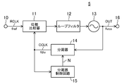
- FIG. 1 shows a configuration of a frequency sweep oscillation circuit for a distance measurement sensor according to an embodiment of the present invention.
- 1 includes an input terminal 10, a phase comparator 11, a loop filter 12, a voltage controlled oscillator (VCO) 13, a frequency divider 14, a frequency divider control circuit 15, and an output. And a terminal 16.
- a reference frequency signal RCLK having a constant reference frequency fref is input to the input terminal 10.
- the reference frequency signal RCLK can be supplied from a crystal oscillator, for example.
- the output terminal 16 is connected to an output frequency signal OUT having a variable output frequency fvco.
- the voltage controlled oscillator 13 outputs an output frequency signal OUT based on the phase comparison signal supplied from the phase comparator 11 via the loop filter 12.
- the frequency divider control circuit 15 outputs a frequency divider control signal that specifies the frequency division ratio N.
- the frequency divider 14 receives the output frequency signal OUT, divides the output frequency signal OUT by the frequency division ratio N specified by the frequency divider control signal, and generates the frequency division frequency signal CCLK having the frequency division frequency fdiv. Output.
- the phase comparator 11 compares the phases of the reference frequency signal RCLK and the divided frequency signal CCLK and outputs a phase comparison signal.
- the frequency divider control circuit 15 receives a frequency division frequency signal CCLK from the frequency divider 14 for timing control. However, the frequency divider control circuit 15 may receive the reference frequency signal RCLK instead of the frequency division frequency signal CCLK.
- fvco fref ⁇ N
- the output frequency fvco changes in proportion to the frequency division ratio N.
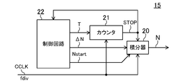
- FIG. 2 shows a detailed configuration example of the frequency divider control circuit 15 in FIG.
- the frequency divider control circuit 15 in FIG. 2 includes an integrator 20, a counter 21, and a control circuit 22.
- the control circuit 22 sends two signals that specify the initial value Nstart of the division ratio and the increment ⁇ N per clock to the integrator 20, and sets the length of the time T in which the increment ⁇ N should be adopted. Signals to be designated are supplied to the counter 21 respectively.
- a frequency divider control signal designating N is output.
- the frequency division ratio N increases with time. If the increment ⁇ N is a negative value, the frequency division ratio N decreases with time. If the increment ⁇ N is 0, The frequency division ratio N is held constant.
- the counter 21 counts the number of clocks of the divided frequency signal CCLK, and outputs the count end signal STOP when the count number corresponds to the set time T, that is, when the time T has elapsed.
- the control circuit 22 updates the three outputs Nstart, ⁇ N, and T.
- the integrator 20 receives the count end signal STOP, the integrator 20 is initialized to the next initial value Nstart.
- FIG. 3A is a graph showing an ideal change with time of the output frequency fvco when the frequency sweep in the up-chirp period is used for the distance measurement sensor.
- the period from time t1 to time t2 is an up chirp period (f1 ⁇ f2) in which the output frequency fvco is linearly increased from the first frequency f1 to the second frequency f2.
- the frequency sweep during this up-chirp period is used for distance measurement.
- the subsequent time t2 to time t4 is a blank period in which the output frequency fvco is returned from the second frequency f2 to the first frequency f1.
- the set of the up chirp period and the blank period is repeated.
- FIG. 3B is a graph showing an example of the division ratio control corresponding to FIG. 3A when the frequency sweep oscillation circuit 5 of FIG. 1 is used.
- the blank period from time t2 to time t4 is divided into a first section from time t2 to time t3 and a second section from time t3 to time t4.
- the frequency division ratio N is a straight line from the second frequency division ratio N2 to the third frequency division ratio N3 that is larger than the first frequency division ratio N1 and smaller than the second frequency division ratio N2. (N1 ⁇ N3 ⁇ N2). In the second section, the frequency division ratio N is linearly decreased from the third frequency division ratio N3 to the first frequency division ratio N1.
- the absolute value of the time change rate (gradient of the graph) of the division ratio N in the decrease of the division ratio N from the third division ratio N3 to the first division ratio N1 in the second section is In order to be smaller than the absolute value of the time change rate (gradient of the graph) of the division ratio N in the decrease of the division ratio N from the second division ratio N2 to the third division ratio N3 in one section. Be controlled.
- FIG. 3C is a graph showing an example of the actual change over time of the output frequency fvco in the case of the frequency division ratio control of FIG.
- the absolute value of the time change rate of the frequency division ratio N is large only in the first section. Therefore, according to FIG. 3C, at the timing of switching from the first section to the second section. Undershoot occurs in the output frequency fvco.
- the fluctuation of the output frequency fvco due to undershoot is predetermined (from the first frequency f1 to the second frequency f2). It is possible to fit within the occupied frequency bandwidth. Further, it becomes easy to ensure the linearity of the frequency sweep at the timing of switching from the blank period to the next up-chirp period (time t4) without extending the blank period.
- FIG. 4A is a graph showing an ideal change with time of the output frequency fvco when the frequency sweep in the down chirp period is used for the distance measurement sensor.
- the period from time t1 to time t2 is a down chirp period (f1> f2) in which the output frequency fvco is linearly lowered from the first frequency f1 to the second frequency f2.
- the frequency sweep during this down chirp period is used for distance measurement.
- the subsequent time t2 to time t4 is a blank period in which the output frequency fvco is returned from the second frequency f2 to the first frequency f1.
- the set of the down chirp period and the blank period is repeated.
- FIG. 4B is a graph showing an example of the division ratio control corresponding to FIG. 4A when the frequency sweep oscillation circuit 5 of FIG. 1 is used.
- the blank period from time t2 to time t4 is divided into a first section from time t2 to time t3 and a second section from time t3 to time t4.
- the frequency division ratio N is a straight line from the second frequency division ratio N2 to a third frequency division ratio N3 that is smaller than the first frequency division ratio N1 and larger than the second frequency division ratio N2. (N1> N3> N2).
- the frequency division ratio N is linearly increased from the third frequency division ratio N3 to the first frequency division ratio N1.
- the time change rate (slope of the graph) of the division ratio N in the increase of the division ratio N from the third division ratio N3 to the first division ratio N1 in the second section is the first section.
- the frequency division ratio N is controlled to be smaller than the time change rate (gradient of the graph) in the increase of the frequency division ratio N from the second frequency division ratio N2 to the third frequency division ratio N3.
- FIG. 4 (c) is a graph showing an example of actual change over time of the output frequency fvco in the case of the frequency division ratio control of FIG. 4 (b). Since the time change rate of the frequency division ratio N in the blank period is large only in the first section, according to FIG. 4C, the output frequency fvco at the timing of switching from the first section to the second section. Overshoot occurs. However, by setting the third frequency division ratio N3 at the time t3 in anticipation of this transient phenomenon, the fluctuation of the output frequency fvco due to overshoot is predetermined (from the first frequency f1 to the second frequency f2). It is possible to fit within the occupied frequency bandwidth. Further, it becomes easy to ensure the linearity of the frequency sweep at the timing of switching from the blank period to the next down chirp period (time t4) without extending the blank period.
- FIG. 5 is a graph showing another example of the division ratio control corresponding to FIG. 3A when the frequency sweep oscillation circuit 5 of FIG. 1 is used.
- the frequency division ratio N is linearly increased from the first frequency division ratio N1 to the second frequency division ratio N2 (N1 ⁇ N2 ).
- the blank period from time t2 to time t5 is divided into a first section from time t2 to time t3, a second section from time t3 to time t4, and a third section from time t4 to time t5. It is done.
- the frequency division ratio N is a straight line from the second frequency division ratio N2 to the third frequency division ratio N3 that is larger than the first frequency division ratio N1 and smaller than the second frequency division ratio N2. (N1 ⁇ N3 ⁇ N2).
- the frequency division ratio N is a straight line from the third frequency division ratio N3 to the fourth frequency division ratio N4 that is larger than the first frequency division ratio N1 and smaller than the third frequency division ratio N3. (N1 ⁇ N4 ⁇ N3).
- the frequency division ratio N is linearly decreased from the fourth frequency division ratio N4 to the first frequency division ratio N1.
- the absolute value of the time change rate (gradient of the graph) of the frequency division ratio N in the decrease of the frequency division ratio N gradually increases from the first section to the second section and from the second section to the third section. It is controlled to be smaller. According to FIG. 5, since the smooth change of the frequency division ratio N in the blank period can be realized as compared with the case of FIG. 3B, the adverse effect of the transient fluctuation occurring in the output frequency fvco can be greatly reduced.
- the time change rate (gradient of the graph) of the frequency division ratio N in the second section from time t3 to time t4 may be zero.
- the absolute value of the time change rate (slope of the graph) of the division ratio N in the third section from time t4 to time t5 is the second section from time t3 to time t4 as long as the value falls below a predetermined value. Control may be performed so as to be larger than the absolute value of the time change rate (gradient of the graph) of the frequency division ratio N.
- the frequency division ratio control is executed by dividing the blank period into three or more sections as illustrated in FIG. It is also possible to do.
- the frequency sweep oscillation circuit according to the present invention has the effect of reducing the adverse effects of transient fluctuations occurring in the output frequency, and is useful as a frequency sweep oscillation circuit for distance measurement sensors and the like.
Landscapes
- Engineering & Computer Science (AREA)
- Computer Networks & Wireless Communication (AREA)
- Physics & Mathematics (AREA)
- General Physics & Mathematics (AREA)
- Radar, Positioning & Navigation (AREA)
- Remote Sensing (AREA)
- Radar Systems Or Details Thereof (AREA)
Abstract
Selon l'invention, un circuit de commande de diviseur de fréquence (15) délivre en sortie, à un diviseur de fréquence (14), un signal de commande de diviseur de fréquence destiné à augmenter un rapport de division de fréquence N d'un premier rapport de division de fréquence à un deuxième rapport de division de fréquence supérieur au premier rapport de division de fréquence pendant une période de piaulement amplifié, à réduire le rapport de division de fréquence N du deuxième rapport de division de fréquence à un troisième rapport de division de fréquence supérieur au premier rapport de division de fréquence mais inférieur au deuxième rapport de division de fréquence pendant une période d'ébauche, et à ramener le rapport de division de fréquence N à un premier rapport de division de fréquence. La commande est exécutée de manière à régler la valeur absolue du taux de variation dans le temps du rapport de division de fréquence N dans la réduction du troisième rapport de division de fréquence au premier rapport de division de fréquence pendant la période d'ébauche de façon à être inférieure à la valeur absolue du taux de variation dans le temps du rapport de division de fréquence N dans la réduction du deuxième rapport de division de fréquence au troisième rapport de division de fréquence pendant la période d'ébauche.
Applications Claiming Priority (2)
| Application Number | Priority Date | Filing Date | Title |
|---|---|---|---|
| JP2016250725 | 2016-12-26 | ||
| JP2016-250725 | 2016-12-26 |
Publications (1)
| Publication Number | Publication Date |
|---|---|
| WO2018123199A1 true WO2018123199A1 (fr) | 2018-07-05 |
Family
ID=62710276
Family Applications (1)
| Application Number | Title | Priority Date | Filing Date |
|---|---|---|---|
| PCT/JP2017/036593 WO2018123199A1 (fr) | 2016-12-26 | 2017-10-10 | Circuit oscillant à balayage de fréquences |
Country Status (1)
| Country | Link |
|---|---|
| WO (1) | WO2018123199A1 (fr) |
Citations (3)
| Publication number | Priority date | Publication date | Assignee | Title |
|---|---|---|---|---|
| JP2011197011A (ja) * | 2000-08-16 | 2011-10-06 | Valeo Radar Systems Inc | 自動車用レーダ・システムおよび方法 |
| JP2012018078A (ja) * | 2010-07-08 | 2012-01-26 | Alouette Technology Inc | チャープ信号生成回路、fmcw方式合成開口レーダ、アンテナ装置及び飛翔体 |
| US20170241825A1 (en) * | 2016-02-22 | 2017-08-24 | Vega Grieshaber Kg | Reduction of power peaks in the spectrum of the mean power of fill level measuring devices |
-
2017
- 2017-10-10 WO PCT/JP2017/036593 patent/WO2018123199A1/fr active Application Filing
Patent Citations (3)
| Publication number | Priority date | Publication date | Assignee | Title |
|---|---|---|---|---|
| JP2011197011A (ja) * | 2000-08-16 | 2011-10-06 | Valeo Radar Systems Inc | 自動車用レーダ・システムおよび方法 |
| JP2012018078A (ja) * | 2010-07-08 | 2012-01-26 | Alouette Technology Inc | チャープ信号生成回路、fmcw方式合成開口レーダ、アンテナ装置及び飛翔体 |
| US20170241825A1 (en) * | 2016-02-22 | 2017-08-24 | Vega Grieshaber Kg | Reduction of power peaks in the spectrum of the mean power of fill level measuring devices |
Similar Documents
| Publication | Publication Date | Title |
|---|---|---|
| US7724097B2 (en) | Direct digital synthesizer for reference frequency generation | |
| US7907023B2 (en) | Phase lock loop with a multiphase oscillator | |
| US7605666B2 (en) | High frequency digital oscillator-on-demand with synchronization | |
| CN106708166B (zh) | 信号生成器和信号生成方法 | |
| KR100824791B1 (ko) | 클록 체배기 및 클록 체배 방법 | |
| US7956696B2 (en) | Techniques for generating fractional clock signals | |
| US11342926B2 (en) | Synchronization of clock signals generated using output dividers | |
| US20060055473A1 (en) | Clock generating circuit | |
| CN107528567B (zh) | 注入锁定振荡器及包括其的半导体器件 | |
| US11342925B2 (en) | Signal generation circuit and method, and digit-to-time conversion circuit and method | |
| JPWO2018116347A1 (ja) | Pll回路 | |
| US20040212410A1 (en) | Reduced-size integrated phase-locked loop | |
| US9602115B1 (en) | Method and apparatus for multi-rate clock generation | |
| US20220052703A1 (en) | Signal generation circuit and method, and digit-to-time conversion circuit and method | |
| US9966963B2 (en) | Frequency synthesizer | |
| US7439812B1 (en) | Auto-ranging phase-locked loop | |
| US10018970B2 (en) | Time-to-digital system and associated frequency synthesizer | |
| EP4175180A1 (fr) | Circuit et procédés de division fractionnaire de signaux d'horloge haute fréquence | |
| WO2018123199A1 (fr) | Circuit oscillant à balayage de fréquences | |
| US20040027181A1 (en) | Clock multiplying PLL circuit | |
| KR20070055011A (ko) | 전압 제어 발진기의 주파수 대역을 안정적으로 조정하는위상 동기 루프 및 방법 | |
| KR100665006B1 (ko) | 위상 동기 루프 장치 | |
| US7276982B1 (en) | High frequency digital oscillator-on-demand with synchronization | |
| GB2368207A (en) | PLL circuit and frequency division method reducing spurious noise | |
| JP2015103895A (ja) | スペクトラム拡散クロック発生回路 |
Legal Events
| Date | Code | Title | Description |
|---|---|---|---|
| 121 | Ep: the epo has been informed by wipo that ep was designated in this application |
Ref document number: 17888114 Country of ref document: EP Kind code of ref document: A1 |
|
| NENP | Non-entry into the national phase |
Ref country code: DE |
|
| 122 | Ep: pct application non-entry in european phase |
Ref document number: 17888114 Country of ref document: EP Kind code of ref document: A1 |
|
| NENP | Non-entry into the national phase |
Ref country code: JP |