WO2018105294A1 - 発光装置、ファイバレーザ、及び、地絡判定方法 - Google Patents
発光装置、ファイバレーザ、及び、地絡判定方法 Download PDFInfo
- Publication number
- WO2018105294A1 WO2018105294A1 PCT/JP2017/040281 JP2017040281W WO2018105294A1 WO 2018105294 A1 WO2018105294 A1 WO 2018105294A1 JP 2017040281 W JP2017040281 W JP 2017040281W WO 2018105294 A1 WO2018105294 A1 WO 2018105294A1
- Authority
- WO
- WIPO (PCT)
- Prior art keywords
- voltage
- light
- light emitting
- emitting device
- ground fault
- Prior art date
- Legal status (The legal status is an assumption and is not a legal conclusion. Google has not performed a legal analysis and makes no representation as to the accuracy of the status listed.)
- Ceased
Links
Images



Classifications
-
- G—PHYSICS
- G01—MEASURING; TESTING
- G01R—MEASURING ELECTRIC VARIABLES; MEASURING MAGNETIC VARIABLES
- G01R31/00—Arrangements for testing electric properties; Arrangements for locating electric faults; Arrangements for electrical testing characterised by what is being tested not provided for elsewhere
- G01R31/50—Testing of electric apparatus, lines, cables or components for short-circuits, continuity, leakage current or incorrect line connections
- G01R31/52—Testing for short-circuits, leakage current or ground faults
-
- H—ELECTRICITY
- H02—GENERATION; CONVERSION OR DISTRIBUTION OF ELECTRIC POWER
- H02H—EMERGENCY PROTECTIVE CIRCUIT ARRANGEMENTS
- H02H11/00—Emergency protective circuit arrangements for preventing the switching-on in case an undesired electric working condition might result
-
- H—ELECTRICITY
- H02—GENERATION; CONVERSION OR DISTRIBUTION OF ELECTRIC POWER
- H02H—EMERGENCY PROTECTIVE CIRCUIT ARRANGEMENTS
- H02H3/00—Emergency protective circuit arrangements for automatic disconnection directly responsive to an undesired change from normal electric working condition with or without subsequent reconnection ; integrated protection
- H02H3/16—Emergency protective circuit arrangements for automatic disconnection directly responsive to an undesired change from normal electric working condition with or without subsequent reconnection ; integrated protection responsive to fault current to earth, frame or mass
-
- H—ELECTRICITY
- H02—GENERATION; CONVERSION OR DISTRIBUTION OF ELECTRIC POWER
- H02H—EMERGENCY PROTECTIVE CIRCUIT ARRANGEMENTS
- H02H7/00—Emergency protective circuit arrangements specially adapted for specific types of electric machines or apparatus or for sectionalised protection of cable or line systems, and effecting automatic switching in the event of an undesired change from normal working conditions
-
- H—ELECTRICITY
- H05—ELECTRIC TECHNIQUES NOT OTHERWISE PROVIDED FOR
- H05B—ELECTRIC HEATING; ELECTRIC LIGHT SOURCES NOT OTHERWISE PROVIDED FOR; CIRCUIT ARRANGEMENTS FOR ELECTRIC LIGHT SOURCES, IN GENERAL
- H05B47/00—Circuit arrangements for operating light sources in general, i.e. where the type of light source is not relevant
- H05B47/10—Controlling the light source
Definitions
- the present invention relates to a light-emitting device including a plurality of light-emitting elements connected in series and having a configuration for determining whether or not a ground fault has occurred.
- the present invention also relates to a fiber laser including such a light emitting device as an excitation light source.
- the present invention also relates to a determination method for determining whether or not a ground fault has occurred in a light emitting device including a plurality of light emitting elements connected in series.
- light emitting devices including a plurality of light emitting elements connected in series (hereinafter also referred to as “light emitting element array”) are widely used.
- a light-emitting device having a laser diode (LD) array is used as an excitation light source.
- a light emitting device having a light emitting diode (LED) array is used as a backlight.
- ground fault refers to a failure in which a point on the current path including the light emitting element array is short-circuited to the ground (including a failure in which a semiconductor inside the light-emitting element is short-circuited to the ground).
- the ground fault is derived, it becomes impossible to normally control the light emitting device. For this reason, in such a light emitting device, there are a configuration for determining whether or not a ground fault has occurred, a configuration for switching the power source to an off state when it is determined that a ground fault has occurred, and the like. Needed.
- Patent Documents 1 and 2 are cited as documents that disclose a light emitting device having a configuration for determining whether or not a ground fault has occurred.
- FIG. 1 of Patent Document 1 shows a light emitting device including a light emitting diode array.
- a configuration is adopted in which a resistor is connected in parallel with the light emitting diode included in the detection target section, and an end point on the downstream side (ground side) of the detection target section is connected to the ground fault detection circuit.
- the determination of the ground fault in this light emitting device is performed in the lighting state after all the DC / DC converters connected to the light emitting diode rows as the power source are turned on (the state in which all the light emitting diodes are lit if no failure has occurred). Done.
- the voltage at the end point on the downstream side of the detection target section decreases to the ground potential. For this reason, it is possible to determine whether or not a ground fault has occurred by detecting this voltage change with the ground fault detection circuit.
- FIG. 12 of Patent Document 2 shows an LED driver that supplies power to a light-emitting diode array.
- this LED driver a configuration is adopted in which a shunt resistor is inserted on the downstream side of the light emitting diode array, and both ends of the section including the shunt resistor are connected to the ground fault detection circuit.
- the determination of the ground fault in the LED driver is performed in the lighting state after the DC / DC converter connected as a power source to the light emitting diode row is switched on. When a ground fault occurs, a part of the current supplied from the DC / DC converter flows out from the short-circuit point to the ground before flowing into the shunt resistor.
- the current flowing through the shunt resistor is reduced as compared with the case where no ground fault occurs, and as a result, the voltage across the shunt resistor is reduced. For this reason, it is possible to determine whether or not a ground fault has occurred by detecting a decrease in the voltage across the shunt resistor with the ground fault detection circuit.
- FIG. 1 of Patent Document 2 also shows an LED driver that supplies power to a light-emitting diode array.
- a diode and a shunt resistor are inserted on the downstream side of the LED array, a detection current output circuit is connected to the upstream end of the diode, and both ends of the section including the diode and the shunt resistor are detected.
- a configuration for connecting to a circuit is employed.
- the determination of the ground fault in the LED driver is performed in the light-off state (a state in which all the light-emitting diodes are turned off if no failure has occurred) before the DC / DC converter connected to the light-emitting diode row as a power source is turned on. Done.
- Japanese Published Patent Publication Japanese Patent Laid-Open No. 2008-251227
- Japanese Published Patent Publication Japanese Published Patent Publication “Japanese Unexamined Patent Application Publication No. 2014-154448” (Publication Date: August 25, 2014)
- the LED driver shown in FIG. 12 of Patent Document 2 and the LED driver shown in FIG. 1 of Patent Document 2 it is much larger than a fixed resistor in determining whether or not a ground fault has occurred. It is necessary to use a large shunt resistance. That is, the LED driver shown in FIG. 12 of Patent Document 2 and the LED driver shown in FIG. 1 of Patent Document 2 have a problem that it is difficult to reduce the size of the device.
- the present invention has been made in view of the above problems, and its purpose is to determine whether a ground fault has occurred or not (a state in which all light-emitting diodes are turned off if no failure has occurred). It is possible to realize a light-emitting device that can be performed at the same time and does not need to use a shunt resistor for the determination.
- a light emitting device includes a current path including a plurality of light emitting elements connected in series and a power source provided upstream of the plurality of light emitting elements, and the current path. And a controller that determines whether or not a ground fault has occurred based on a voltage across the section including at least one light emitting element.
- a determination method includes a light emission including a current path including a plurality of light-emitting elements connected in series and a power source provided upstream of the plurality of light-emitting elements.
- a determination method for determining whether or not a ground fault has occurred in an apparatus the step of determining whether or not a ground fault has occurred based on a voltage at both ends of a section including at least one light emitting element in the current path. It is characterized by including.
- a light-emitting device that can determine whether or not a ground fault has occurred in a light-off state and does not need to use a shunt resistor for the determination.
- FIG. 1 is a circuit block diagram of a light emitting device according to an embodiment of the present invention. It is a timing chart which shows normal operation
- FIG. 3 is a circuit diagram illustrating a second configuration example of a voltage detection circuit included in the light emitting device illustrated in FIG. 1.
- FIG. 1 is a circuit block diagram of a light emitting device 1 according to the present embodiment.
- the light emitting device 1 includes a current path 11, a voltage detection circuit 12, and an LD control unit 13 (corresponding to a “control unit” in the claims).
- the light emitting device 1 is included in an optical device such as a fiber laser as a light source such as an excitation light source, and is controlled by the main control unit 2 of the optical device.
- the current path 11 includes a power source PS, a plurality (six in this embodiment) of laser diodes LD1 to LD6 (corresponding to “light emitting elements” in the claims), a switch SW, and a shunt resistor SR (patented) Equivalent to “resistors” in the claims) is inserted in this order in series. That is, the power supply PS has a negative electrode grounded and a positive electrode connected to the anode of the laser diode LD1.
- the laser diode LD1 has an anode connected to the positive electrode of the power source PS and a cathode connected to the anode of the laser diode LD2.
- the laser diode LD6 has an anode connected to the cathode of the laser diode LD5 and a cathode connected to one end of the switch SW.
- the switch SW has one end connected to the cathode of the laser diode LD6 and the other end connected to one end of the shunt resistor SR.
- the shunt resistor SR has one end connected to the other end of the switch SW and the other end grounded.
- the switching between the ON state and the OFF state of the power supply PS is performed by the main control unit 2, and the switching between the ON state and the OFF state of the switch SW is performed by the LD control unit 13.
- the drive current supplied from the power source PS is a current path. 11
- the laser diodes LD1 to LD6 emit light by this drive current.
- the voltage detection circuit 12 includes a voltage VPQ at both ends of the target section including at least one laser diode (only the laser diode LD1 provided at the most upstream in this embodiment) in the current path 11, that is, an end point on the upstream side of the target section.
- the voltage detection circuit 12 determines whether or not the both-end voltage VPQ exceeds the threshold voltage Vth, and provides a detection signal indicating the determination result to the LD control unit 13.
- a configuration example of the voltage detection circuit 12 will be described later with reference to another drawing.
- the LD control unit 13 switches the switch SW from the off state to the on state based on the light emission start command from the main control unit 2. Further, the LD control unit 13 determines whether a ground fault has occurred, and provides the main control unit 2 with an alarm signal ALM indicating the determination result. The LD control unit 13 performs this determination processing based on the detection signal from the voltage detection circuit 12 when (1) the power source PS is in an on state and the switch SW is in an off state, and (2 ) When the power source PS is in the on state and the switch SW is in the on state, the determination is performed based on the voltage VSR across the shunt resistor SR.
- the both-ends voltage VPQ of the interval of interest changes depending on whether or not a ground fault occurs downstream of the cathode of the laser diode LD1). That is, when no ground fault occurs downstream from the end point Q of the target section, no current flows through the laser diode LD1 included in the target section, and thus the both-ends voltage VPQ of the target section becomes zero.
- the switch SW when the switch SW is turned on, that is, when the power source PS is in an on state and the switch SW is in an off state, a ground fault occurs upstream of the shunt resistor SR in the current path 11.
- the voltage VSR across the shunt resistor SR changes depending on whether it occurs. That is, when a ground fault does not occur on the upstream side of the shunt resistor SR, all the current supplied from the power source PS flows through the shunt resistor SR, so the voltage VSR across the shunt resistor SR has a predetermined value.
- the section including the laser diode LD1 in order to determine whether or not a ground fault has occurred in the case where the power source PS is on and the switch SW is off.
- a configuration is adopted in which the voltage between both ends VPQ of the target interval is referred to as the interval, but the present invention is not limited to this. That is, (a) a configuration in which a section including a laser diode LDi (2 ⁇ i ⁇ 6) other than the laser diode LD1 is set as a target section may be employed, or (b) a plurality of lasers arranged adjacent to each other.
- a configuration may be adopted in which a section including the diodes LDi to LDj (1 ⁇ i ⁇ 5, i ⁇ j ⁇ 6) is a section of interest.
- the end point Q of the target section (the cathode of the laser diode LDi is referred to by referring to the both-end voltage VPQ of the target section. It is possible to determine whether or not a ground fault has occurred on the downstream side of ().
- the voltage VPQ at both ends of the target section including the laser diode LD3 is referred to. It is possible to determine whether or not a ground fault has occurred on the downstream side of the end point Q of the target section (the cathode of the laser diode LDj disposed on the most downstream side in the target section). For example, it is possible to determine whether or not a ground fault has occurred on the downstream side of the cathode of LD3 by referring to the voltage VPQ across the section including the three laser diodes LD1 to LD3.
- the both-ends voltage VPQ of the attention section varies depending on the location where the ground fault occurs.
- a ground fault occurs downstream of the cathode of the laser diode LD3
- both ends of about 1.7V ⁇ 3 5.1V
- the both-ends voltage VPQ of the attention section when a ground fault occurs between the cathode of the most upstream laser diode LDi in the attention section and the anode of the most downstream laser diode LDj in the attention section, the both-ends voltage VPQ of the attention section.
- the location where the ground fault occurred can be specified from the size of the.
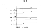
- FIG. 2 is a timing chart illustrating the operation of the light emitting device 1 when no ground fault occurs.
- the main control unit 2 switches the power supply PS from the off state to the on state, and raises the power supply voltage VPS from 0V to, for example, 24V.
- the state of the switch SW is kept in the off state which is the initial state. For this reason, if a ground fault does not occur downstream of the cathode of the laser diode LD1, no drive current flows through the laser diode LD1, and the laser diode LD1 does not light up. Therefore, the both-ends voltage VPQ in the attention interval is kept at 0 V even after the power source PS is switched to the on state.
- the main control unit 2 issues a light emission start command. This is given to the LD control unit 13.
- the LD control unit 13 that has received the light emission start command switches the switch SW from the off state to the on state.
- both the power supply PS and the switch SW are turned on, the drive current flows through the current path 11, and the laser diodes LD1 to LD6 emit light.
- the both-ends voltage VPQ in the attention interval also rises from 0V to, for example, 1.7V.
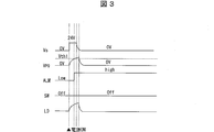
- FIG. 3 is a timing chart showing the operation of the light emitting device 1 when a ground fault occurs before the operation starts.
- the main control unit 2 switches the power supply PS from the off state to the on state, and raises the power supply voltage VPS from 0V to, for example, 24V.
- the state of the switch SW is kept in the off state which is the initial state.
- a ground fault occurs downstream of the cathode of the laser diode LD1
- a drive current flows through the laser diode LD1
- the laser diode LD1 is turned on. Therefore, the both-ends voltage VPQ of the target section including the laser diode LD1 rises after the power supply PS is switched to the on state.
- the voltage detection circuit 12 changes the value of the detection signal from the low level (indicating that VPQ ⁇ Vth) to the high level (indicating that VPQ> Vth). Switch to.
- the LD control unit 13 switches the value of the alarm signal ALM from the low level to the high level.
- the main control unit 2 switches the power source PS from the on state to the off state, and decreases the power source voltage VPS.
- the power supply voltage VPS is lowered, the laser diode LD1 is turned off, and the both-ends voltage VPQ in the target section is lowered.
- FIG. 3 in order to clarify the causal relationship, the timing at which each operation described in this paragraph occurs is shifted, but these operations occur continuously in a short time.
- the main control unit 2 emits light because the alarm signal is at a high level (indicating that a ground fault has occurred) when the predetermined time ⁇ t has elapsed since the power source PS was switched on. A start command is not given to the LD control unit 13. Therefore, the switch SW is kept in the off state.
- the LD control unit 13 determines that the voltage VPQ between both ends of the attention interval is equal to the predetermined threshold voltage Vth when the power source PS is in the on state and the switch SW is in the off state. It is determined that a ground fault has occurred when the value is higher. Thereby, it is possible to detect a ground fault occurring before the operation is started immediately after the operation is started.
- a section including a plurality of laser diodes LDi to LDj is set as an attention section
- a configuration in which a place where a ground fault has occurred may be adopted from the magnitude of the voltage VPQ at both ends of the attention section.
- the laser when it is determined that a ground fault has occurred on the downstream side of the cathode of the diode LD3, and (2) the laser voltage when the both-ends voltage VPQ of the target section becomes about 3.4V (for example, 2.55V or more and less than 4.25V).
- the laser voltage when the both-ends voltage VPQ of the target section becomes about 1.7V (for example, 0.85V or more and less than 2.55V).
- a configuration can be adopted in which it is determined that a ground fault has occurred between the cathode of the diode LD1 and the anode of the laser diode LD2.
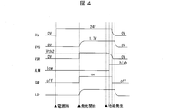
- FIG. 4 is a timing chart showing the operation of the light emitting device 1 when a ground fault occurs after the operation starts.
- the timing chart of FIG. 4 shows the voltage VSR across the shunt resistor SR in addition to the timing chart of FIG.
- the LD control unit 13 When the LD control unit 13 detects that the voltage VSR across the shunt resistor SR is lower than the threshold voltage Vth2 when the switch SW is in the ON state, the LD control unit 13 switches the value of the alarm signal ALM from the low level to the high level. When the value of the alarm signal ALM is switched to the high level, the main control unit 2 switches the power source PS from the on state to the off state, and decreases the power source voltage VPS. When the power supply voltage VPS decreases, the laser diodes LD1 to LDi are extinguished, and the both-ends voltage VPQ in the interval of interest decreases. In FIG. 4, the timing at which each operation described in this paragraph occurs is shifted, but these operations occur continuously in a short time.
- the LD control unit 13 determines that the voltage VSR across the shunt resistor SR is lower than the predetermined threshold voltage Vth2 when the power source PS is in the on state and the switch SW is in the on state. It is determined that a ground fault has occurred. Thereby, it is possible to detect a ground fault that has occurred after the start of operation immediately after the occurrence of the ground fault.
- FIG. 5 is a circuit diagram showing a first configuration example of the voltage detection circuit 12.
- the voltage detection circuit 12 shown in FIG. 5 includes a first voltage dividing circuit R1, a second voltage dividing circuit R2, a subtracting circuit S, and a comparator (comparing circuit) C.
- the subtraction circuit S has resistors Ra to Rd and an operational amplifier OP.
- the first voltage dividing circuit R1 is a circuit for dividing the voltage VP at the end point P on the upstream side of the section of interest. (1) One end is connected to the end point P, and the other end is connected to one end of the voltage dividing resistor R12. The voltage dividing resistor R11, and (2) a voltage dividing resistor R12 having one end connected to the other end of the voltage dividing resistor R11 and the other end grounded.
- R12 / (R11 + R12) ⁇
- the second voltage dividing circuit R2 is a circuit for dividing the voltage VP at the end point Q on the downstream side of the section of interest. (1) One end is connected to the end point Q and the other end is connected to one end of the voltage dividing resistor R22. And (2) a voltage dividing resistor R22 having one end connected to the other end of the voltage dividing resistor R21 and the other end grounded.
- R22 / (R21 + R22) ⁇
- the subtracting circuit S is a circuit for subtracting the output voltage VR2 of the second voltage dividing circuit R2 from the output voltage VR1 of the first voltage dividing circuit R1, and (1) the operational amplifier OP and (2) one end of the first voltage dividing circuit R1.
- An input resistor Ra connected to the voltage circuit R1, the other end connected to the inverting input of the operational amplifier OP; and (3) one end connected to the second voltage dividing circuit R2 and the other end connected to the non-inverting input of the operational amplifier OP.
- a grounding resistor Rd having the other end grounded.
- the comparator C is an element for comparing the output voltage VS of the subtraction circuit S with the reference voltage Vref.
- the output of the comparator C is a detection signal that takes a high level when the both-ends voltage VPQ of the interval of interest exceeds the threshold voltage Vth, and takes a low level when the both-ends voltage VPQ of the interval of interest falls below the threshold voltage Vth. This is supplied to the LD controller 13 described above.
- FIG. 6 illustrates a second configuration example of the voltage detection circuit 12 with reference to FIG. 6.
- FIG. 6 is a circuit diagram showing a second configuration example of the voltage detection circuit 12.
- the voltage detection circuit 12 shown in FIG. 6 includes a transistor TR, a voltage dividing circuit R1, and a diode D.
- the transistor TR is a PNP type bipolar transistor. (1) The emitter is connected to the end point P on the upstream side of the target section, and (2) the base is connected to the end point Q on the downstream side of the target section via the diode D. (3) The collector is grounded via the voltage dividing circuit R1. When the both-ends voltage VPQ of the attention interval, that is, the base-emitter voltage of the transistor TR exceeds the threshold voltage Vth, the collector voltage Vc of the transistor TR is applied to the voltage dividing circuit R1. Note that the diode D inserted between the base of the transistor TR and the end point Q of the section of interest has a configuration for compensating the forward voltage Vf when no drive current flows through the laser diode LD1.
- the voltage dividing circuit R1 is a circuit for dividing the collector voltage Vc of the transistor TR. (1) A voltage dividing resistor having one end connected to the collector of the transistor TR and the other end connected to one end of the voltage dividing resistor R12. R11, and (2) a voltage dividing resistor R12 having one end connected to the other end of the voltage dividing resistor R11 and the other end grounded, and (3) a Zener diode TD connected in parallel to the voltage dividing resistor R12. Has been.
- the output of the voltage dividing circuit R1 is a detection signal that takes a high level when the both-ends voltage VPQ of the target section is higher than the threshold voltage Vth, and takes a low level when the both-ends voltage VPQ of the target section is lower than the threshold voltage Vth. , And supplied to the LD control unit 13 described above.
- the Zener diode TD connected in parallel with the voltage dividing resistor R12 has a configuration for overcurrent protection. It is also possible to replace the Zener diode TD with another element having an overcurrent protection function or to omit it.
- the light emitting device (1) includes a current path (11) including a plurality of light emitting elements connected in series and a power source (PS) provided upstream of the plurality of light emitting elements, and the current path.
- the determination method includes a light emitting device (1) including a current path (11) including a plurality of light emitting elements connected in series and a power source (PS) provided upstream of the plurality of light emitting elements.
- the method for determining whether or not a ground fault has occurred, and whether or not a ground fault has occurred based on a voltage (VPQ) across the section including at least one light emitting element in the current path (11) A step of determining whether or not.
- a ground fault has occurred on the downstream side of the at least one light-emitting element is determined in a light-off state (a state in which all light-emitting diodes are turned off if no failure has occurred, for example.
- the determination can be made when the power source (PS) provided upstream of the plurality of light-emitting elements is in an on state and the switch (SW) provided downstream of the plurality of light-emitting elements is in an off state.
- PS power source
- SW switch
- the current path (11) further includes a switch (SW) provided downstream of the plurality of light emitting elements
- the control unit (13) includes the power source ( When PS) is in the on state and the switch (SW) is in the off state, a ground fault occurs when the voltage across the both ends (VPQ) exceeds a predetermined threshold voltage (Vth). It is preferable to determine.
- the current path (11) further includes a resistor (SR), the control unit (13) has the power source (PS) in an on state, and When the switch (SW) is in an ON state, it is determined that a ground fault has occurred when the voltage (VSR) across the resistor (SR) is lower than a predetermined threshold voltage (Vth2). It is preferable.
- SR resistor
- PS power source
- Vth2 predetermined threshold voltage
- whether or not a ground fault has occurred downstream of the at least one light emitting element can be determined not only in the light-off state but also in the light-on state.
- the at least one light emitting element is a light emitting element provided on the most upstream side among the plurality of light emitting elements.
- the light emitting device (1) includes a first voltage dividing circuit (R1) that divides the voltage at one end of the section, and a second voltage dividing circuit (R2) that divides the voltage at the other end of the section.
- the subtracting circuit (S) for subtracting the output voltage (VR2) of the second voltage dividing circuit (R2) from the output voltage (VR1) of the first voltage dividing circuit (R1), and the output of the subtracting circuit (S)
- Vth predetermined threshold voltage
- the control unit (13) is configured to provide a ground fault based on the output voltage of the comparison circuit (C). It is preferable to determine whether or not the above has occurred.
- the light emitting device (1) divides the collector voltage of the transistor (TR) and the transistor (TR) having the emitter connected to one end of the section and the base connected to the other end of the section. And a voltage dividing circuit (R1).
- the control unit (13) preferably determines whether or not a ground fault has occurred based on an output voltage of the voltage dividing circuit (R1).
- the base of the transistor (TR) is connected to the other end of the section via a diode.
- the forward voltage can be compensated when no dynamic current flows through the at least one light emitting element.
- the light emitting element is preferably a laser diode (LD1, LD2,).
- the section includes a plurality of light emitting elements, and the control unit (13) has a ground fault in the current path (11) based on the voltage across the section. It is preferable to identify the location where it occurs.
- a fiber laser including the light emitting device (1) as an excitation light source is also included in the scope of the present invention.
Landscapes
- Physics & Mathematics (AREA)
- General Physics & Mathematics (AREA)
- Circuit Arrangement For Electric Light Sources In General (AREA)
- Emergency Protection Circuit Devices (AREA)
- Protection Of Static Devices (AREA)
- Testing Of Short-Circuits, Discontinuities, Leakage, Or Incorrect Line Connections (AREA)
Abstract
地絡が生じているか否かの判定を消灯状態において行うことが可能であり、且つ、その判定にシャント抵抗を用いる必要がない発光装置を実現する。発光装置(1)は、複数のレーザダイオード(LD1~LD6)とその上流に設けられた電源(PS)とを含む電流路(11)と、レーザダイオード(LD1)を含む区間の両端電圧(VPQ)に基づいて、地絡が生じているか否かを判定するLD制御部(13)と、を備えている。
Description
本発明は、直列に接続された複数の発光素子を備えた発光装置であって、地絡が生じているか否かを判定するための構成を備えた発光装置に関する。また、そのような発光装置を励起光源として備えたファイバレーザに関する。また、直列に接続された複数の発光素子を備えた発光装置において、地絡が生じているか否かを判定する判定方法に関する。
各種装置の各種光源として、直列に接続された複数の発光素子(以下、「発光素子列」とも記載)を備えた発光装置が広く用いられている。例えば、ファイバレーザにおいては、レーザダイオード(LD:Laser Diode)列を備えた発光装置が、励起光源として用いられている。或いは、テレビジョン受像機においては、発光ダイオード(LED:Light Emitting Diode)列を備えた発光装置が、バックライトとして用いられている。
このような発光装置においては、「地絡」と呼ばれる故障が生じることがある。ここで、地絡とは、発光素子列を含む電流路上の点がグランドと短絡する故障(発光素子内部の半導体がグランドと短絡する故障を含む)のことを指す。地絡が派生すると、発光装置を正常に制御することが不可能になる。このため、このような発光装置においては、地絡が生じているか否かを判定するための構成や、地絡が生じていると判定された場合に電源をオフ状態に切り替えるための構成などが必要とされる。
地絡が生じているか否かを判定するための構成を備えた発光装置を開示した文献としては、例えば、特許文献1~2が挙げられる。
特許文献1の図1には、発光ダイオード列を備えた発光装置が示されている。この発光装置においては、検出対象区間に含まれる発光ダイオードと並列に抵抗を接続すると共に、検出対象区間の下流側(グランド側)の端点を地絡検出回路に接続する構成が採用されている。この発光装置における地絡の判定は、発光ダイオード列に電源として接続されたDC/DCコンバータをオン状態に切り替えた後に点灯状態(故障が発生していなければ全ての発光ダイオードが点灯する状態)において行われる。検出対象区間において地絡が生じると、検出対象区間の下流側の端点の電圧が接地電位まで低下する。このため、この電圧の変化を地絡検出回路で検出することによって、地絡が生じているか否かを判定することができる。
特許文献2の図12には、発光ダイオード列に電力を供給するLEDドライバが示されている。このLEDドライバにおいては、発光ダイオード列の下流側にシャント抵抗を挿入し、シャント抵抗を含む区間の両端を地絡検出回路に接続する構成が採用されている。このLEDドライバにおける地絡の判定は、発光ダイオード列に電源として接続されたDC/DCコンバータをオン状態に切り替えた後に点灯状態において行われる。地絡が生じると、DC/DCコンバータから供給された電流の一部がシャント抵抗に流入する前に短絡点からグランドに流出する。したがって、地絡が生じていない場合と比べて、シャント抵抗を流れる電流が少なくなり、その結果、シャント抵抗の両端電圧が小さくなる。このため、シャント抵抗の両端電圧の低下を地絡検出回路で検出することによって、地絡が生じているか否かを判定することができる。
特許文献2の図1にも、発光ダイオード列に電力を供給するLEDドライバが示されている。このLEDドライバにおいては、発光ダイオード列の下流側にダイオード及びシャント抵抗を挿入し、ダイオードの上流側の端部に検知電流出力回路を接続し、ダイオード及びシャント抵抗を含む区間の両端を地絡検出回路に接続する構成が採用されている。このLEDドライバにおける地絡の判定は、発光ダイオード列に電源として接続されたDC/DCコンバータをオン状態に切り替える前に消灯状態(故障が発生していなければ全ての発光ダイオードが消灯する状態)において行われる。地絡が生じると、検知電流出力回路から供給された電流の一部がダイオード及びシャント抵抗に流入する前に短絡点からグランドに流出する。したがって、地絡が生じていない場合と比べて、ダイオード及びシャント抵抗を流れる電流が少なくなり、ダイオード及びシャント抵抗の両端電圧が小さくなる。このため、シャント抵抗の両端電圧の低下を地絡検出回路で検出することによって、地絡が生じているか否かを判定することができる。
特許文献1の図1に記載の発光装置、及び、特許文献2の図12に記載のLEDドライバにおいては、地絡が生じているか否かの判定を、点灯状態において行う必要がある。すなわち、特許文献1の図1に記載の発光装置、及び、特許文献2の図12に記載のLEDドライバにおいては、地絡が生じているか否かの判定を、消灯状態において行うことができないという問題があった。
また、特許文献2の図12に記載のLEDドライバ、及び、特許文献2の図1に記載のLEDドライバにおいては、地絡が生じているか否かの判定に、固定抵抗と比べて格段にサイズの大きいシャント抵抗を用いる必要がある。すなわち、特許文献2の図12に記載のLEDドライバ、及び、特許文献2の図1に記載のLEDドライバにおいては、装置の小型化が困難であるという問題があった。
本発明は、上記の問題に鑑みてなされたものであり、その目的は、地絡が生じているか否かの判定を消灯状態(故障が発生していなければ全ての発光ダイオードが消灯する状態)において行うことが可能であり、且つ、その判定にシャント抵抗を用いる必要がない発光装置を実現することにある。
上記の課題を解決するために、本発明に係る発光装置は、直列に接続された複数の発光素子と上記複数の発光素子の上流に設けられた電源とを含む電流路と、上記電流路において少なくとも1つの発光素子を含む区間の両端電圧に基づいて、地絡が生じているか否かを判定する制御部と、を備えている、ことを特徴とする。
また、上記の課題を解決するために、本発明に係る判定方法は、直列に接続された複数の発光素子と上記複数の発光素子の上流に設けられた電源とを含む電流路を備えた発光装置において、地絡が生じているか否かを判定する判定方法であって、上記電流路において少なくとも1つの発光素子を含む区間の両端電圧に基づいて地絡が生じているか否かを判定する工程を含む、ことを特徴とする。
本発明によれば、地絡が生じているか否かの判定を消灯状態において行うことが可能であり、且つ、その判定にシャント抵抗を用いる必要がない発光装置を実現することができる。
(発光装置の構成)
本発明の一実施形態に係る発光装置1の構成について、図1を参照して説明する。図1は、本実施形態に係る発光装置1の回路ブロック図である。
本発明の一実施形態に係る発光装置1の構成について、図1を参照して説明する。図1は、本実施形態に係る発光装置1の回路ブロック図である。
発光装置1は、電流路11と、電圧検知回路12と、LD制御部13(特許請求の範囲における「制御部」に相当)と、を備えている。発光装置1は、ファイバレーザ等の光学装置に、励起光源等の光源として含まれ、その光学装置の主制御部2によって制御される。
電流路11には、電源PSと、複数(本実施形態においては6個)のレーザダイオードLD1~LD6(請求項の範囲における「発光素子」に相当)と、スイッチSWと、シャント抵抗SR(特許請求の範囲における「抵抗体」に相当)とが、この順に直列に挿入されている。すなわち、電源PSは、負極が接地され、正極がレーザダイオードLD1のアノードに接続されている。レーザダイオードLD1は、アノードが電源PSの正極に接続され、カソードがレーザダイオードLD2のアノードに接続されている。レーザダイオードLDi(i=2~5)は、アノードがレーザダイオードLDi-1のカソードに接続され、カソードがLDi+1のアノードに接続されている。レーザダイオードLD6は、アノードがレーザダイオードLD5のカソードに接続され、カソードがスイッチSWの一端に接続されている。スイッチSWは、一端がレーザダイオードLD6のカソードに接続され、他端がシャント抵抗SRの一端に接続されている。シャント抵抗SRは、一端がスイッチSWの他端に接続され、他端が接地されている。
電源PSのオン状態とオフ状態との切り替えは、主制御部2によって行われ、スイッチSWのオン状態とオフ状態との切り替えは、LD制御部13によって行われる。主制御部2によって電源PSがオフ状態からオン状態へと切り替えられた後、LD制御部13によってスイッチSWがオフ状態からオン状態へと切り替えられると、電源PSから供給された駆動電流が電流路11を流れ、この駆動電流によってレーザダイオードLD1~LD6が発光する。
電圧検知回路12は、電流路11において少なくとも1つのレーザダイオード(本実施形態においては最も上流に設けられたレーザダイオードLD1のみ)を含む注目区間の両端電圧VPQ、すなわち、注目区間の上流側の端点Pの電圧VPと当該区間の下流側の端点Qの電圧VQとの電位差VPQ=VP-VQを検知するための回路である。電圧検知回路12は、両端電圧VPQが閾値電圧Vthを上回っているか否かを判定し、判定結果を示す検知信号をLD制御部13に提供する。なお、電圧検知回路12の構成例については、参照する図面を代えて後述する。
LD制御部13は、主制御部2からの発光開始命令に基づいてスイッチSWをオフ状態からオン状態へと切り替える。また、LD制御部13は、地絡が生じているかを判定し、判定結果を示すアラーム信号ALMを主制御部2に提供する。LD制御部13は、この判定処理を、(1)電源PSがオン状態にあり、且つ、スイッチSWがオフ状態にある場合には、電圧検知回路12からの検知信号に基づいて行い、(2)電源PSがオン状態にあり、且つ、スイッチSWがオン状態にある場合には、シャント抵抗SRの両端電圧VSRに基づいて行う。
電源PSをオン状態に切り替えてからスイッチSWをオン状態に切り替えるまでの期間、すなわち、電源PSがオン状態であり、且つ、スイッチSWがオフ状態である場合、電流路11において注目区間の端点Q(本実施形態においては、レーザダイオードLD1のカソード)よりも下流側で地絡が生じているか否かに応じて、注目区間の両端電圧VPQが変化する。すなわち、注目区間の端点Qよりも下流側で地絡が生じていない場合、注目区間に含まれるレーザダイオードLD1に電流は流れないため、注目区間の両端電圧VPQはゼロになる。一方、注目区間の端点Qよりも下流側で地絡が生じている場合、注目区間に含まれるレーザダイオードLD1に電流が流れるため、注目区間の両端電圧VPQがゼロでない値(例えば、1.7V)を持つ。したがって、電源PSがオン状態であり、且つ、スイッチSWがオフ状態である場合、注目区間に0でない両端電圧VPQが生じるか否かに基づいて、注目区間の端点Qよりも下流側で地絡が生じているか否かを判定することができる。詳細については、後述する「地絡が発生していない場合の発光装置の動作」及び「動作開始前に地絡が発生した場合の発光装置の動作」を参照されたい。
また、スイッチSWをオン状態に切り替えてからの期間、すなわち、電源PSがオン状態であり、且つ、スイッチSWがオフ状態である場合、電流路11においてシャント抵抗SRよりも上流側で地絡が生じているか否かに応じて、シャント抵抗SRの両端電圧VSRが変化する。すなわち、シャント抵抗SRよりも上流側で地絡が生じていない場合、電源PSから供給された電流が全てシャント抵抗SRを流れるので、シャント抵抗SRの両端電圧VSRは所定の値を持つ。一方、シャント抵抗SRよりも上流側で地絡が生じている場合、電源PSから供給された電流の一部(又は全部)が地絡を生じた点からグランドに流出し、シャント抵抗SRに流入する電流が減少する(又はゼロになる)ので、シャント抵抗SRの両端電圧VSRは所定の値よりも小さくなる(又はゼロになる)。したがって、電源PSがオン状態であり、且つ、スイッチSWがオフ状態である場合、シャント抵抗の両端電圧VSRが所定の値よりも小さくなっているか否かに基づいて、シャント抵抗SRよりも上流側で地絡が生じているか否かを判定することができる。詳細については、後述する「動作開始後に地絡が発生した場合の発光装置の動作」を参照されたい。
なお、本実施形態においては、電源PSがオン状態であり、且つ、スイッチSWがオフ状態である場合に関して、地絡が生じているか否かを判定するために、レーザダイオードLD1を含む区間を注目区間とし、この注目区間の両端電圧VPQを参照する構成を採用しているが、本発明はこれに限定されない。すなわち、(a)レーザダイオードLD1以外のレーザダイオードLDi(2≦i≦6)を含む区間を注目区間とする構成を採用してもよいし、(b)互いに隣接して配置された複数のレーザダイオードLDi~LDj(1≦i≦5,i<j≦6)を含む区間を注目区間とする構成を採用してもよい。レーザダイオードLDi(2≦i≦6)を含む区間を注目区間とする構成(a)を採用した場合、注目区間の両端電圧VPQを参照することよって、注目区間の端点Q(レーザダイオードLDiのカソード)よりも下流側で地絡が生じているか否かを判定することができる。例えば、レーザダイオードLD3を含む注目区間の両端電圧VPQを参照することによって、LD3のカソードよりも下流側で地絡が生じているか否かを判定することができる。また、複数のレーザダイオードLDi~LDj(1≦i≦5,i<j≦6)を含む区間を注目区間とする構成(b)を採用した場合、注目区間の両端電圧VPQを参照することよって、注目区間の端点Q(注目区間のなかで最も下流側に配置されたレーザダイオードLDjのカソード)よりも下流側で地絡が生じているか否かを判定することができる。例えば、3つのレーザダイオードLD1~LD3を含む区間の両端電圧VPQを参照することによって、LD3のカソードよりも下流側で地絡が生じているか否かを判定することができる。
なお、複数のレーザダイオードLDi~LDjを含む区間を注目区間とする構成(b)を採用した場合には、地絡が起きた場所によって注目区間の両端電圧VPQが変化する。例えば、3つのレーザダイオードLD1~LD3を含む区間を注目区間とする構成を採用した場合、レーザダイオードLD3のカソードよりも下流側で地絡が起きると1.7V×3=5.1V程度の両端電圧VPQが生じるのに対して、レーザダイオードLD2のカソードとレーザダイオードLD3のアノードとの間で地絡が起きると1.7×2=3.4V程度の両端電圧VPQが生じ、レーザダイオードLD1のカソードとレーザダイオードLD2のアノードとの間で地絡を生じると1.7V程度の両端電圧VPQが生じる。したがって、注目区間のなかで最も上流側のレーザダイオードLDiのカソードと注目区間のなかで最も下流側のレーザダイオードLDjのアノードとの間で地絡が起きた場合には、注目区間の両端電圧VPQの大きさから地絡が起きた場所を特定することもできる。
(地絡が発生していない場合の発光装置の動作)
次に、地絡が発生していない場合の発光装置1の動作(正常動作)について、図2を参照して説明する。図2は、地絡が発生していない場合における発光装置1の動作を示すタイミングチャートである。
次に、地絡が発生していない場合の発光装置1の動作(正常動作)について、図2を参照して説明する。図2は、地絡が発生していない場合における発光装置1の動作を示すタイミングチャートである。
まず、主制御部2が、電源PSをオフ状態からオン状態へと切り替え、電源電圧VPSを0Vから例えば24Vに上昇させる。スイッチSWの状態は、初期状態であるオフ状態に保たれている。このため、レーザダイオードLD1のカソードよりも下流側で地絡が発生していなければ、レーザダイオードLD1に駆動電流が流れることはなく、レーザダイオードLD1が点灯することもない。したがって、注目区間の両端電圧VPQは、電源PSがオン状態に切り替えられた後も0Vに保たれる。
主制御部2は、電源PSをオン状態に切り替えた時点から所定の時間Δtが経過した時点でアラーム信号がローレベル(地絡が発生していないことを示す)である場合、発光開始命令をLD制御部13に与える。発光開始命令を受けたLD制御部13は、スイッチSWをオフ状態からオン状態へと切り替える。これにより、電源PS及びスイッチSWの両方がオン状態となり、駆動電流が電流路11を流れ、レーザダイオードLD1~LD6が発光する。このとき、注目区間の両端電圧VPQも、0Vから例えば1.7Vに上昇する。
(動作開始前に地絡が発生した場合の発光装置の動作)
次に、動作開始前に地絡が発生した場合の発光装置1の動作について、図3を参照して説明する。図3は、動作開始前に地絡が発生した場合の発光装置1の動作を示すタイミングチャートである。
次に、動作開始前に地絡が発生した場合の発光装置1の動作について、図3を参照して説明する。図3は、動作開始前に地絡が発生した場合の発光装置1の動作を示すタイミングチャートである。
まず、主制御部2が、電源PSをオフ状態からオン状態へと切り替え、電源電圧VPSを0Vから例えば24Vに上昇させる。スイッチSWの状態は、初期状態であるオフ状態に保たれている。しかしながら、レーザダイオードLD1のカソードよりも下流側で地絡が発生していると、レーザダイオードLD1に駆動電流が流れ、レーザダイオードLD1が点灯する。したがって、レーザダイオードLD1を含む注目区間の両端電圧VPQは、電源PSがオン状態に切り替えられた後に上昇する。
注目区間の両端電圧VPQが閾値電圧Vthを上回ると、電圧検知回路12は、検知信号の値をローレベル(VPQ<Vthであることを示す)からハイレベル(VPQ>Vthであることを示す)に切り替える。検知信号の値がハイレベルに切り替わると、LD制御部13は、アラーム信号ALMの値をローレベルからハイレベルに切り替える。アラーム信号ALMの値がハイレベルに切り替わると、主制御部2は、電源PSをオン状態からオフ状態へと切り替え、電源電圧VPSを低下させる。電源電圧VPSが低下すると、レーザダイオードLD1が消灯し、注目区間の両端電圧VPQが低下する。なお、図3では、因果関係を明らかにするために、本段落にて説明した各動作が起こるタイミングをずらして示しているが、これらの動作は短時間のうちに連続して起こる。
なお、主制御部2は、電源PSをオン状態に切り替えた時点から上記所定の時間Δtが経過した時点でアラーム信号がハイレベル(地絡が発生していることを示す)であるため、発光開始命令をLD制御部13に与えない。したがって、スイッチSWは、オフ状態に保たれる。
以上のように、発光装置1において、LD制御部13は、電源PSがオン状態にあり、且つ、スイッチSWがオフ状態にある場合、注目区間の両端電圧VPQが予め定められた閾値電圧Vthを上回っているときに地絡が生じていると判定する。これにより、動作開始前に発生した地絡を、動作開始後直ちに検出することができる。
なお、複数のレーザダイオードLDi~LDjを含む区間を注目区間とする場合には、注目区間の両端電圧VPQの大きさから地絡が起きた場所を特定する構成を採用してもよい。例えば、3つのレーザダイオードLD1~LD3を含む区間を注目区間とする場合には、(1)注目区間の両端電圧VPQが5.1V程度(例えば、4.25V以上)となったときに、レーザダイオードLD3のカソードよりも下流側で地絡が起きたと判定し、(2)注目区間の両端電圧VPQが3.4V程度(例えば、2.55V以上4.25V未満)となったときに、レーザダイオードLD3のカソードよりも下流側で地絡が起きたと判定し、(3)注目区間の両端電圧VPQが1.7V程度(例えば、0.85V以上2.55V未満)となったときに、レーザダイオードLD1のカソードとレーザダイオードLD2のアノードとの間で地絡が起きたと判定する判定する構成を採用することができる。
(動作開始後に地絡が発生した場合の発光装置の動作)
次に、動作開始後に地絡が発生した場合の発光装置1の動作について、図4を参照して説明する。図4は、動作開始後に地絡が発生した場合の発光装置1の動作を示すタイミングチャートである。なお、図4のタイミングチャートには、図2のタイミングチャートに加え、シャント抵抗SRの両端電圧VSRを図示している。
次に、動作開始後に地絡が発生した場合の発光装置1の動作について、図4を参照して説明する。図4は、動作開始後に地絡が発生した場合の発光装置1の動作を示すタイミングチャートである。なお、図4のタイミングチャートには、図2のタイミングチャートに加え、シャント抵抗SRの両端電圧VSRを図示している。
レーザダイオードLD1~LD6が発光を開始してから注目区間の両端電圧VPQが0Vから例えば1.7Vに変化するまでの動作は、図2のタイミングチャートと同じであるため、ここではその説明を省略する。
スイッチSWをオン状態に切り替えると、シャント抵抗SRに駆動電流が流れ、シャント抵抗SRの両端電圧VSRが上昇する。その後、レーザダイオードLD1~LD6のいずれかにおいて地絡が発生すると、シャント抵抗SRを流れる駆動電流が減少し、その結果、シャント抵抗SRの両端電圧VSRも減少する。完全な地絡が生じた場合には、シャント抵抗SRを流れる駆動電流が0になり、その結果、シャント抵抗SRの両端電圧VSRも0になる。
LD制御部13は、スイッチSWがオン状態にあるときにシャント抵抗SRの両端電圧VSRが閾値電圧Vth2を下回ったことを検知すると、アラーム信号ALMの値をローレベルからハイレベルに切り替える。アラーム信号ALMの値がハイレベルに切り替わると、主制御部2は、電源PSをオン状態からオフ状態へと切り替え、電源電圧VPSを低下させる。電源電圧VPSが低下すると、レーザダイオードLD1~LDiが消灯し、注目区間の両端電圧VPQが低下する。なお、図4では、本段落にて説明した各動作が起こるタイミングをずらして示しているが、これらの動作は短時間のうちに連続して起こる。
以上のように、発光装置1において、LD制御部13は、電源PSがオン状態にあり、スイッチSWがオン状態にある場合、シャント抵抗SRの両端電圧VSRが予め定められた閾値電圧Vth2を下回っているときに地絡が生じていると判定する。これにより、動作開始後に発生した地絡を、地絡発生後直ちに検出することができる。
(電圧検知回路の構成例1)
次に、電圧検知回路12の第1の構成例について、図5を参照して説明する。図5は、電圧検知回路12の第1の構成例を示す回路図である。
次に、電圧検知回路12の第1の構成例について、図5を参照して説明する。図5は、電圧検知回路12の第1の構成例を示す回路図である。
図5に示す電圧検知回路12は、第1分圧回路R1、第2分圧回路R2、減算回路S、及びコンパレータ(比較回路)Cを備えている。減算回路Sは、抵抗Ra~抵抗Rd、ならびにオペアンプOPを有している。
第1分圧回路R1は、注目区間の上流側の端点Pの電圧VPを分圧するための回路であり、(1)一端が端点Pに接続され、他端が分圧抵抗R12の一端に接続された分圧抵抗R11と、(2)一端が分圧抵抗R11の他端に接続され、他端が接地された分圧抵抗R12とにより構成されている。R12/(R11+R12)=αとすると、第1分圧回路R1の出力電圧VR1は、VR1=αVPとなる。
第2分圧回路R2は、注目区間の下流側の端点Qの電圧VPを分圧するための回路であり、(1)一端が端点Qに接続され、他端が分圧抵抗R22の一端に接続された分圧抵抗R21と、(2)一端が分圧抵抗R21の他端に接続され、他端が接地された分圧抵抗R22とにより構成されている。R22/(R21+R22)=αとすると、第2分圧回路R2の出力電圧VR2は、VR2=αVQとなる。
減算回路Sは、第1分圧回路R1の出力電圧VR1から第2分圧回路R2の出力電圧VR2を減算するための回路であり、(1)オペアンプOPと、(2)一端が第1分圧回路R1に接続され、他端がオペアンプOPの反転入力に接続された入力抵抗Raと、(3)一端が第2分圧回路R2に接続され、他端がオペアンプOPの非反転入力に接続された入力抵抗Rbと、(4)一端がオペアンプOPの出力に接続され、他端がオペアンプOPの反転入力に接続された帰還抵抗Rcと、(5)一端がオペアンプOPの非反転入力に接続され、他端が接地された接地抵抗Rdと、により構成されている。Rc/Ra=Rd/Rb=1とすると、減算回路Sの出力電圧VSは、VS=VR2-VR1=α(VQ-VP)となる。
コンパレータCは、減算回路Sの出力電圧VSを基準電圧Vrefと比較するための素子である。基準電圧Vrefは、上述した閾値電圧Vthのα倍に設定されている。したがって、コンパレータCは、注目区間の両端電圧VPQ=VQ-VPを閾値電圧Vthと比較していると言い換えることができる。このコンパレータCの出力は、注目区間の両端電圧VPQが閾値電圧Vthを上回っているときハイレベルを取り、注目区間の両端電圧VPQが閾値電圧Vthを下回っているときローレベルを取る検知信号として、上述したLD制御部13に供給される。
(電圧検知回路の構成例2)
図6は、電圧検知回路12の第2の構成例について、図6を参照して説明する。図6は、電圧検知回路12の第2の構成例を示す回路図である。
図6は、電圧検知回路12の第2の構成例について、図6を参照して説明する。図6は、電圧検知回路12の第2の構成例を示す回路図である。
図6に示す電圧検知回路12は、トランジスタTR、分圧回路R1、及びダイオードDを備えている。
トランジスタTRは、PNPタイプのバイポーラトランジスタであり、(1)エミッタが注目区間の上流側の端点Pと接続され、(2)ベースがダイオードDを介して注目区間の下流側の端点Qと接続され、(3)コレクタが分圧回路R1を介して接地されている。注目区間の両端電圧VPQ、すなわち、トランジスタTRのベース・エミッタ間電圧が閾値電圧Vthを超えると、トランジスタTRのコレクタ電圧Vcが分圧回路R1に印加される。なお、トランジスタTRのベースと注目区間の端点Qとの間に挿入されたダイオードDは、レーザダイオードLD1に駆動電流が流れていないときに順方向電圧Vfを補償するための構成である。
分圧回路R1は、トランジスタTRのコレクタ電圧Vcを分圧するための回路であり、(1)一端がトランジスタTRのコレクタに接続され、他端が分圧抵抗R12の一端に接続された分圧抵抗R11と、(2)一端が分圧抵抗R11の他端に接続され、他端が接地された分圧抵抗R12と、(3)分圧抵抗R12に並列に接続されたツェナダイオードTDとにより構成されている。分圧回路R1の出力は、注目区間の両端電圧VPQが閾値電圧Vthを上回っているときハイレベルを取り、注目区間の両端電圧VPQが閾値電圧Vthを下回っているときローレベルを取る検知信号として、上述したLD制御部13に供給される。なお、分圧抵抗R12と並列に接続されたツェナダイオードTDは、過電流保護のための構成である。ツェナダイオードTDを、過電流保護機能を有する他の素子に置き換えたり、省略したりすることも可能である。
(まとめ)
本実施形態に係る発光装置(1)は、直列に接続された複数の発光素子と上記複数の発光素子の上流に設けられた電源(PS)とを含む電流路(11)と、上記電流路(11)において少なくとも1つの発光素子を含む区間の両端電圧(VPQ)に基づいて、地絡が生じているか否かを判定する制御部(13)と、を備えている、ことを特徴とする。
本実施形態に係る発光装置(1)は、直列に接続された複数の発光素子と上記複数の発光素子の上流に設けられた電源(PS)とを含む電流路(11)と、上記電流路(11)において少なくとも1つの発光素子を含む区間の両端電圧(VPQ)に基づいて、地絡が生じているか否かを判定する制御部(13)と、を備えている、ことを特徴とする。
本実施形態に係る判定方法は、直列に接続された複数の発光素子と上記複数の発光素子の上流に設けられた電源(PS)とを含む電流路(11)を備えた発光装置(1)において、地絡が生じているか否かを判定する判定方法であって、上記電流路(11)において少なくとも1つの発光素子を含む区間の両端電圧(VPQ)に基づいて地絡が生じているか否かを判定する工程を含む、ことを特徴とする。
上記の構成によれば、上記少なくとも1つの発光素子よりも下流側で地絡が生じているか否かを、消灯状態(故障が発生していなければ全ての発光ダイオードが消灯する状態、例えば、上記複数の発光素子の上流に設けられた電源(PS)がオン状態にあり、且つ、上記複数の発光素子の下流に設けられたスイッチ(SW)がオフ状態)において判定することができる。しかも、その判定に、シャント抵抗を用いる必要がない。
本実施形態に係る発光装置(1)において、上記電流路(11)は、上記複数の発光素子の下流に設けられたスイッチ(SW)を更に含み、上記制御部(13)は、上記電源(PS)がオン状態にあり、且つ、上記スイッチ(SW)がオフ状態にある場合、上記両端電圧(VPQ)が予め定められた閾値電圧(Vth)を上回っているときに地絡が生じていると判定する、ことが好ましい。
上記の構成によれば、上記少なくとも1つの発光素子よりも下流側で地絡が生じているか否かを、消灯状態において判定する。しかも、その判定に、シャント抵抗を用いる必要がない。
本実施形態に係る発光装置(1)において、上記電流路(11)は、抵抗体(SR)を更に含み、上記制御部(13)は、上記電源(PS)がオン状態にあり、且つ、上記スイッチ(SW)がオン状態にある場合、上記抵抗体(SR)の両端電圧(VSR)が予め定められた閾値電圧(Vth2)を下回っているときに地絡が生じていると判定する、ことが好ましい。
上記の構成によれば、上記少なくとも1つの発光素子よりも下流側で地絡が生じているか否かを、消灯状態においてのみならず、点灯状態においても判定することができる。
本実施形態に係る発光装置(1)において、上記少なくとも1つの発光素子は、上記複数の発光素子のうち最も上流に設けられた発光素子である、ことが好ましい。
上記の構成によれば、最も上流に設けられた発光素子よりも下流側において生じた地絡を漏れなく検出することができる。
本実施形態に係る発光装置(1)は、上記区間の一端の電圧を分圧する第1分圧回路(R1)と、上記区間の他端の電圧を分圧する第2分圧回路(R2)と、上記第1分圧回路(R1)の出力電圧(VR1)から上記第2分圧回路(R2)の出力電圧(VR2)を減算する減算回路(S)と、上記減算回路(S)の出力電圧(VS)を予め定められた閾値電圧(Vth)と比較する比較回路(C)と、を更に備え、上記制御部(13)は、上記比較回路(C)の出力電圧に基づいて地絡が生じているか否かを判定する、ことが好ましい。
上記の構成によれば、上記少なくとも1つの発光素子よりも下流側で地絡が生じているか否かを、消灯状態において精度良く判定することができる。
本実施形態に係る発光装置(1)は、上記区間の一端にエミッタが接続され、上記区間の他端にベースが接続されたトランジスタ(TR)と、上記トランジスタ(TR)のコレクタ電圧を分圧する分圧回路(R1)と、を更に備え、上記制御部(13)は、上記分圧回路(R1)の出力電圧に基づいて地絡が生じているか否かを判定する、ことが好ましい。
上記の構成によれば、上記少なくとも1つの発光素子よりも下流側で地絡が生じているか否かを、消灯状態において精度良く判定することができる。
本実施形態に係る発光装置(1)において、上記トランジスタ(TR)のベースは、ダイオードを介して上記区間の上記他端に接続されている、ことが好ましい。
上記の構成によれば、上記少なくとも1つの発光素子に動電流が流れていないときに順方向電圧を補償することができる。
本実施形態に係る発光装置(1)において、上記発光素子は、レーザダイオード(LD1,LD2,…)である、ことが好ましい。
上記の構成によれば、上記発光素子が発光ダイオードである発光装置(1)よりも強い光を発する光源を実現することができる。
本実施形態に係る発光装置(1)において、上記区間は、複数の発光素子を含み、上記制御部(13)は、上記区間の両端電圧に基づいて、上記電流路(11)において地絡が生じている箇所を特定する、ことが好ましい。
上記の構成によれば、上記少なくとも1つの発光素子よりも下流側で地絡が生じているか否かに加えて、上記電流路(11)の何処で地絡が生じているかを特定することができる。
なお、上記の発光装置(1)を励起光源として含むファイバレーザも本発明の範疇に含まれる。
(付記事項)
本発明は上述した各実施形態に限定されるものではなく、請求項に示した範囲で種々の変更が可能であり、異なる実施形態にそれぞれ開示された技術的手段を適宜組み合わせて得られる実施形態についても本発明の技術的範囲に含まれる。
本発明は上述した各実施形態に限定されるものではなく、請求項に示した範囲で種々の変更が可能であり、異なる実施形態にそれぞれ開示された技術的手段を適宜組み合わせて得られる実施形態についても本発明の技術的範囲に含まれる。
1 発光装置
11 電流路
12 電圧検知回路
13 LD制御部(制御部)
PS 電源
LD1~LD6 レーザダイオード(発光素子)
SW スイッチ
SR シャント抵抗(抵抗体)
11 電流路
12 電圧検知回路
13 LD制御部(制御部)
PS 電源
LD1~LD6 レーザダイオード(発光素子)
SW スイッチ
SR シャント抵抗(抵抗体)
Claims (11)
- 直列に接続された複数の発光素子と上記複数の発光素子の上流に設けられた電源とを含む電流路と、
上記電流路において少なくとも1つの発光素子を含む区間の両端電圧に基づいて、地絡が生じているか否かを判定する制御部と、を備えている、
ことを特徴とする発光装置。 - 上記電流路は、上記複数の発光素子の下流に設けられたスイッチを更に含み、
上記制御部は、上記電源がオン状態にあり、且つ、上記スイッチがオフ状態にある場合、上記両端電圧が予め定められた閾値電圧を上回っているときに地絡が生じていると判定する、
ことを特徴とする請求項1に記載の発光装置。 - 上記電流路は、抵抗体を更に含み、
上記制御部は、上記電源がオン状態にあり、且つ、上記スイッチがオン状態にある場合、上記抵抗体の両端電圧が予め定められた閾値電圧を下回っているときに地絡が生じていると判定する、
ことを特徴とする請求項2に記載の発光装置。 - 上記少なくとも1つの発光素子は、上記複数の発光素子のうち最も上流に設けられた発光素子である、
ことを特徴とする請求項1~3の何れか1項に記載の発光装置。 - 上記区間の一端の電圧を分圧する第1分圧回路と、
上記区間の他端の電圧を分圧する第2分圧回路と、
上記第1分圧回路の出力電圧から上記第2分圧回路の出力電圧を減算する減算回路と、
上記減算回路の出力電圧を予め定められた閾値電圧と比較する比較回路と、を更に備え、
上記制御部は、上記比較回路の出力電圧に基づいて地絡が生じているか否かを判定する、
ことを特徴とする請求項1~4の何れか1項に記載の発光装置。 - 上記区間の一端にエミッタが接続され、上記区間の他端にベースが接続されたトランジスタと、
上記トランジスタのコレクタ電圧を分圧する分圧回路と、を更に備え、
上記制御部は、上記分圧回路の出力電圧に基づいて地絡が生じているか否かを判定する、
ことを特徴とする請求項1~4の何れか1項に記載の発光装置。 - 上記トランジスタのベースは、ダイオードを介して上記区間の上記他端に接続されている、
ことを特徴とする請求項6に記載の発光装置。 - 上記発光素子は、レーザダイオードである、
ことを特徴とする請求項1~7の何れか1項に記載の発光装置。 - 上記区間は、複数の発光素子を含み、
上記制御部は、上記区間の両端電圧に基づいて、上記電流路において地絡が生じている箇所を特定する、
ことを特徴とする請求項1~8までの何れか1項に記載の発光装置。 - 請求項1~9の何れか1項に記載の発光装置を励起光源として含む、
ことを特徴とするファイバレーザ。 - 直列に接続された複数の発光素子と上記複数の発光素子の上流に設けられた電源とを含む電流路を備えた発光装置において、地絡が生じているか否かを判定する判定方法であって、
上記電流路において少なくとも1つの発光素子を含む区間の両端電圧に基づいて地絡が生じているか否かを判定する工程を含んでいる、
ことを特徴とする判定方法。
Applications Claiming Priority (2)
| Application Number | Priority Date | Filing Date | Title |
|---|---|---|---|
| JP2016239552A JP6351696B2 (ja) | 2016-12-09 | 2016-12-09 | 発光装置、ファイバレーザ、及び、地絡判定方法 |
| JP2016-239552 | 2016-12-09 |
Publications (1)
| Publication Number | Publication Date |
|---|---|
| WO2018105294A1 true WO2018105294A1 (ja) | 2018-06-14 |
Family
ID=62490907
Family Applications (1)
| Application Number | Title | Priority Date | Filing Date |
|---|---|---|---|
| PCT/JP2017/040281 Ceased WO2018105294A1 (ja) | 2016-12-09 | 2017-11-08 | 発光装置、ファイバレーザ、及び、地絡判定方法 |
Country Status (2)
| Country | Link |
|---|---|
| JP (1) | JP6351696B2 (ja) |
| WO (1) | WO2018105294A1 (ja) |
Families Citing this family (2)
| Publication number | Priority date | Publication date | Assignee | Title |
|---|---|---|---|---|
| US12336072B2 (en) | 2019-10-22 | 2025-06-17 | Signify Holding B.V. | LED driver and lighting system using the same |
| KR20220120026A (ko) * | 2021-02-22 | 2022-08-30 | 주식회사 엘지에너지솔루션 | 배터리 관리 장치 |
Citations (3)
| Publication number | Priority date | Publication date | Assignee | Title |
|---|---|---|---|---|
| JP2012160436A (ja) * | 2011-01-13 | 2012-08-23 | Rohm Co Ltd | Ledショート検出回路、led駆動装置、led照明装置、車両 |
| JP2016088296A (ja) * | 2014-11-05 | 2016-05-23 | ローム株式会社 | 発光素子駆動装置、発光装置、車両 |
| JP2016195041A (ja) * | 2015-03-31 | 2016-11-17 | 株式会社フジクラ | 光源装置 |
-
2016
- 2016-12-09 JP JP2016239552A patent/JP6351696B2/ja not_active Expired - Fee Related
-
2017
- 2017-11-08 WO PCT/JP2017/040281 patent/WO2018105294A1/ja not_active Ceased
Patent Citations (3)
| Publication number | Priority date | Publication date | Assignee | Title |
|---|---|---|---|---|
| JP2012160436A (ja) * | 2011-01-13 | 2012-08-23 | Rohm Co Ltd | Ledショート検出回路、led駆動装置、led照明装置、車両 |
| JP2016088296A (ja) * | 2014-11-05 | 2016-05-23 | ローム株式会社 | 発光素子駆動装置、発光装置、車両 |
| JP2016195041A (ja) * | 2015-03-31 | 2016-11-17 | 株式会社フジクラ | 光源装置 |
Also Published As
| Publication number | Publication date |
|---|---|
| JP6351696B2 (ja) | 2018-07-04 |
| JP2018097973A (ja) | 2018-06-21 |
Similar Documents
| Publication | Publication Date | Title |
|---|---|---|
| US8035310B2 (en) | Circuit for driving light source | |
| ES2978762T3 (es) | Circuito de detección de interrupción LED | |
| US8144111B2 (en) | Light emitting diode driving circuit having voltage detection | |
| US8878445B2 (en) | Light-emitting element driving device | |
| JP2010135136A (ja) | Led点灯装置 | |
| US20180279455A1 (en) | Led failure detecting device | |
| CN111091780B (zh) | 像素电路及其修复方法 | |
| JP2011171547A (ja) | 発光ダイオードの故障検出回路 | |
| US11076473B2 (en) | Method for detecting a defect in an LED string and electronic circuit with at least one LED string | |
| JP6351696B2 (ja) | 発光装置、ファイバレーザ、及び、地絡判定方法 | |
| US8853969B1 (en) | Light emitting element drive device | |
| JP6341139B2 (ja) | 発光装置 | |
| JP2009016459A (ja) | 駆動装置及び照明装置 | |
| US20130249420A1 (en) | Led driving system and method | |
| WO2015145742A1 (ja) | レーザダイオードの駆動回路及びレーザ装置 | |
| JP2015147445A (ja) | 車両用灯具およびその駆動装置 | |
| KR20130056085A (ko) | 발광소자부 쇼트 보호 회로 | |
| JP6314743B2 (ja) | 発光装置 | |
| US11382194B2 (en) | Lighting circuit | |
| JP4817368B2 (ja) | 火災感知器 | |
| JP7106966B2 (ja) | 車両用灯具 | |
| KR101174237B1 (ko) | Led 구동전압 조절회로 및 led 구동 시스템 | |
| JP2008146836A (ja) | 照明装置 | |
| JP4277643B2 (ja) | 複数のledによる表示灯装置 | |
| JP4123134B2 (ja) | レーザ駆動装置 |
Legal Events
| Date | Code | Title | Description |
|---|---|---|---|
| 121 | Ep: the epo has been informed by wipo that ep was designated in this application |
Ref document number: 17879088 Country of ref document: EP Kind code of ref document: A1 |
|
| NENP | Non-entry into the national phase |
Ref country code: DE |
|
| 122 | Ep: pct application non-entry in european phase |
Ref document number: 17879088 Country of ref document: EP Kind code of ref document: A1 |