WO2018096847A1 - 電源回路装置 - Google Patents
電源回路装置 Download PDFInfo
- Publication number
- WO2018096847A1 WO2018096847A1 PCT/JP2017/037799 JP2017037799W WO2018096847A1 WO 2018096847 A1 WO2018096847 A1 WO 2018096847A1 JP 2017037799 W JP2017037799 W JP 2017037799W WO 2018096847 A1 WO2018096847 A1 WO 2018096847A1
- Authority
- WO
- WIPO (PCT)
- Prior art keywords
- winding
- power
- transformer
- power supply
- circuit
- Prior art date
- Legal status (The legal status is an assumption and is not a legal conclusion. Google has not performed a legal analysis and makes no representation as to the accuracy of the status listed.)
- Ceased
Links
Images

Classifications
-
- H—ELECTRICITY
- H02—GENERATION; CONVERSION OR DISTRIBUTION OF ELECTRIC POWER
- H02M—APPARATUS FOR CONVERSION BETWEEN AC AND AC, BETWEEN AC AND DC, OR BETWEEN DC AND DC, AND FOR USE WITH MAINS OR SIMILAR POWER SUPPLY SYSTEMS; CONVERSION OF DC OR AC INPUT POWER INTO SURGE OUTPUT POWER; CONTROL OR REGULATION THEREOF
- H02M3/00—Conversion of DC power input into DC power output
- H02M3/22—Conversion of DC power input into DC power output with intermediate conversion into AC
- H02M3/24—Conversion of DC power input into DC power output with intermediate conversion into AC by static converters
- H02M3/28—Conversion of DC power input into DC power output with intermediate conversion into AC by static converters using discharge tubes with control electrode or semiconductor devices with control electrode to produce the intermediate AC
Definitions
- the present invention relates to a power supply circuit device, and more particularly to a power supply circuit device used in a power conversion device that drives a rotating electrical machine for driving a vehicle.
- the power conversion device Since it is necessary to provide a plurality of power supply voltages in a power conversion device that drives a rotating electrical machine for driving a vehicle, the power conversion device includes a power supply circuit device having a plurality of transformers (Patent Document 1).
- the input energy of both transformers varies depending on the variation of the self-inductance of the winding connected to the input side power supply.
- the output energy of both transformers varies depending on the variation in power consumption of the output side load. The larger the input energy, the higher the voltage on the output side load, and the larger the output energy, the lower the voltage on the output side load.
- An object of the present invention is to reduce variations in the voltage of the output side load caused by variations in self-inductance and variations in power consumption of the load, and to improve the reliability of the power supply circuit device.
- a flyback type power supply circuit device includes a first transformer and a second transformer connected in series with a winding connected to an input power supply together with the first transformer, the first transformer comprising: A fourth winding having a first winding connected to the input power source, a second winding connected to the first output load, and a third winding, the second transformer being connected in series with the first winding.
- a fifth winding connected to the second output load, a sixth winding, and the third winding and the sixth winding receive power from the first transformer and the second transformer.
- the third winding supplies more power than the sixth winding to the power consumption circuit.
- the sixth winding is the third Supplying more than a line power to the power circuit.
- the reliability of the power supply circuit device can be improved.
- FIG. 1 is an overall circuit configuration diagram centering on a power supply circuit 100.
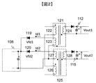
- FIG. FIG. 2 is a circuit configuration diagram of a part of a power supply circuit 100 centering on a transformer 121 and a transformer 125 in FIG. 1.
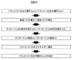
- 3 is an operation flow of the circuit shown in FIG. 2.
- one winding of two transformers connected in series is connected in parallel to the power consuming circuit.
- the power consumption circuit is configured to increase the power supplied by the transformer having the higher output voltage.
- FIG. 1 is an overall circuit configuration diagram centering on the power supply circuit 100.
- the power supply circuit 100 includes a startup circuit 101, a power supply IC 103, a diode 104 and a diode 105, a resistor 106, a Zener diode 107, a voltage monitoring circuit 108, a voltage dividing resistor 109, a transistor 110, a transformer 121, and a transformer. 125, a diode 111, a diode 114, a diode 119 and a diode 120, and a capacitor 112 and a capacitor 115.
- the power supply circuit 100 is a flyback power supply circuit, and increases or decreases the voltage of the battery 102 to supply power to the load 113 and the load 116.
- the startup circuit 101 is a circuit that is supplied with power from the battery 102 and temporarily supplies power to the power supply IC 103.
- the battery 102 a nickel metal hydride battery or a lithium ion battery is used.
- the contactor 117 is for conducting or blocking between the battery 102 and the smoothing capacitor 118.
- the power supply IC 103 monitors the voltage divided by the voltage dividing resistor 109 in the voltage monitoring circuit 108 and transmits an on / off signal to the transistor 110 so as to keep the voltage constant.
- the diode 104 and the diode 105 supply power from the battery 102 to the power supply IC 103 via the startup circuit 101 at the time of startup, and when the capacitor in the voltage monitoring circuit 108 exceeds a predetermined voltage after startup, power is supplied to the power supply IC 103 from the capacitor.
- the circuit is configured.
- the resistor 106 adjusts the current supplied to the power supply IC 103.
- the Zener diode 107 is for clamping a voltage applied to the power supply terminal of the power supply IC 103.
- the transformer 121 is composed of three windings: a winding 122 connected to the battery 102 side, a winding 123 connected to the voltage monitoring circuit 108, and a winding 124 connected to the load 113 side.
- the transformer 125 includes three windings: a winding 126 connected to the battery 102 side, a winding 127 connected to the voltage monitoring circuit 108, and a winding 128 connected to the load 116 side.
- the winding 122 is the first winding
- the winding 124 is the second winding
- the winding 123 is the third winding
- the winding 126 is the fourth winding
- the winding 128 is the fifth winding
- the winding 127 Corresponds to the sixth winding.
- the winding 122 is connected in parallel to the voltage monitoring circuit 108 via the diode 126, the winding 123 is connected in series, the winding 123 is connected via the diode 119, and the winding 127 is connected via the diode 120.
- the transistor 110 accumulates energy in the windings 122 and 126 of the transformer 121 and the transformer 125 when conducting.
- the energy stored in the battery-side winding when the transistor 110 is cut off is transmitted to the load 113 and the load 116 through the cores and gaps of the transformer 121 and transformer 125.
- the diode 111 and the diode 114 block the current of the windings of the transformer 121 and the transformer 125 when the transistor 110 is turned on, and are turned on when the transistor 111 is turned off to charge the capacitor 112 and the capacitor 115.
- the capacitor 112 and the capacitor 115 are for stabilizing the voltage applied to the load 113 and the load 116.
- FIG. 2 is a circuit configuration diagram of a part of the power supply circuit 100 centering on the transformer 121 and the transformer 125 of FIG.
- FIG. 3 is an operation flow of the circuit shown in FIG.
- Vout2 is the output voltage of the transformer 125, that is, the voltage of the capacitor 115.
- Vfd1 is a forward voltage of the diode 119. Id1 is a current flowing through the diode 119. Vfd2 is a forward voltage of the diode 120. Id2 is a current flowing through the diode 120.
- the operation flow in FIG. 3 explains the flow until the voltage difference between Vout1 and Vout2 decreases when Vout1 is larger than Vout2.
- Vout1 is larger than Vout2, that is, the self-inductance of the winding 122 is larger than the self-inductance of the winding 126, or the power consumption of the load 113 is smaller than the load 116.
- the voltage of the winding 123 of the transformer 121 is larger than the voltage of the winding 127 of the transformer 125.
- the forward voltage Vfd1 of the diode 119 becomes larger than the forward voltage Vfd2 of the diode 120.
- the current Id1 of the diode 119 is larger than the current Id2 of the diode 120.
- the power supplied by the transformer 121 is larger than the transformer 125 in the power consumed by the voltage monitoring circuit 108.
- the output energy of the transformer 121 increases and Vout1 decreases. That is, the voltage monitoring circuit 108 functions as a power consumption circuit.
- the voltage monitoring circuit 108 functions as a power consumption circuit, but a circuit having another function may function as a power consumption circuit.
- wiring becomes easy, and an increase in size of the device can be suppressed.
- Vout2 When Vout2 is larger than Vout1, the voltage of Vout2 decreases in the same flow as when Vout1 is larger than Vout2. As described above, variations in output voltage can be reduced.
- DESCRIPTION OF SYMBOLS 100 ... Power supply circuit, 101 ... Starting circuit, 102 ... Battery, 103 ... Power supply IC, 104 ... Diode, 105 ... Diode, 106 ... Resistance, 107 ... Zener diode, 108 ... Voltage monitoring circuit, 109 ... Voltage dividing resistor, 110 ... Transistor, 111 ... Diode, 112 ... Capacitor, 113 ... Load, 114 ... Diode, 115 ... Capacitor, 116 ... Load, 117 ... Contactor, 118 ... Smoothing capacitor, 119 ... Diode, 120 ... Diode, 121 ... Transformer, 122 ... Winding Wire, 123 ... winding, 124 ... winding, 125 ... transformer, 126 ... winding, 127 ... winding, 128 ... winding
Landscapes
- Engineering & Computer Science (AREA)
- Power Engineering (AREA)
- Dc-Dc Converters (AREA)
Abstract
負荷の消費電力のばらつきにより生じる出力側負荷の電圧のばらつきを軽減し、電源回路装置の信頼性を向上させることである。 フライバック方式の電源回路装置は、第1トランスと、第2トランスと、を備え、前記第1トランスは、入力電源と繋がる第1巻線と、第1出力負荷と繋がる第2巻線と、第3巻線と、を有し、前記第2トランスは、前記第1巻線と直列に繋がる第4巻線と、第2出力負荷と繋がる第5巻線と、第6巻線と、を有し、前記第3巻線及び前記第6巻線は、前記第1トランス及び前記第2トランスの電力を消費する電力消費回路に接続され、第1出力負荷の出力電圧が第2出力負荷の出力電圧より高い場合は、第3巻線が第6巻線より多い電力を前記電力消費回路に供給し、第2出力負荷の出力電圧が第1出力負荷の出力電圧より高い場合は、第6巻線が第3巻線より多い電力を前記電力消費回路に供給する。
Description
本発明は、電源回路装置に関し、特に車両駆動用回転電機を駆動する電力変換装置に用いられる電源回路装置に関する。
車両駆動用回転電機を駆動する電力変換装置には複数の電源電圧を設ける必要があるので、電力変換装置は複数のトランスを有する電源回路装置を備える(特許文献1)。
直列接続される2つのトランスにおいて入力側電源に接続される巻線の自己インダクタンスのばらつきによって、両トランスの入力エネルギーが異なる。また、出力側負荷の消費電力のばらつきによって両トランスの出力エネルギーが異なる。入力エネルギーが大きいほど出力側負荷の電圧が高くなり、出力エネルギーが大きいほど出力側負荷の電圧が低くなる。
このように、自己インダクタンスや負荷の消費電力がばらつく場合、入力エネルギー、及び出力エネルギーのバランスが両トランスの間で異なる。そのため、特許文献に記載された電源回路の場合、出力電圧が異なってしまう。
本発明の課題は、自己インダクタンスのばらつきや、負荷の消費電力のばらつきにより生じる出力側負荷の電圧のばらつきを軽減し、電源回路装置の信頼性を向上させることである。
本発明に係るフライバック方式の電源回路装置は、第1トランスと、前記第1トランスとともに入力電源に接続する巻線が直列に接続される第2トランスと、を備え、前記第1トランスは、入力電源と繋がる第1巻線と、第1出力負荷と繋がる第2巻線と、第3巻線と、を有し、前記第2トランスは、前記第1巻線と直列に繋がる第4巻線と、第2出力負荷と繋がる第5巻線と、第6巻線と、を有し、前記第3巻線及び前記第6巻線は、前記第1トランス及び前記第2トランスの電力を消費する電力消費回路に接続され、第1出力負荷の出力電圧が第2出力負荷の出力電圧より高い場合は、第3巻線が第6巻線より多い電力を前記電力消費回路に供給し、第2出力負荷の出力電圧が第1出力負荷の出力電圧より高い場合は、第6巻線が第3巻線より多い電力を前記電力消費回路に供給する。
本発明により、電源回路装置の信頼性を向上させることができる。
本発明の実施形態に入る前に、本実施形態の原理を以下に説明する。
本実施形態では直列接続する2つのトランスのうち1巻線を電力消費回路に並列接続する。電力消費回路に関しては出力電圧が大きい方のトランスが供給する電力を大きくする構成とする。
これにより、電力消費回路による消費電力を出力電圧の大きい方に集中させ、出力電圧が大きい方のトランスの出力エネルギーを増大させることで、出力電圧を低下させ、出力電圧のばらつきを軽減する。
つまり、直列接続する両トランスのうち入力側電源に接続される巻線の自己インダクタンスのばらつきや、トランスの出力側負荷の消費電力が異なる場合において、出力側負荷の電圧ばらつきを軽減できる。
以下、本発明に係る実施形態を図面を用いて詳説する。
図1は、電源回路100を中心にした全体回路構成図である。
電源回路100は、起動回路101と、電源IC103と、ダイオード104及びダイオード105と、抵抗106と、ツェナーダイオード107と、電圧監視回路108と、分圧抵抗109と、トランジスタ110と、トランス121及びトランス125と、ダイオード111、ダイオード114、ダイオード119及びダイオード120と、コンデンサ112及びコンデンサ115と、を有する。
電源回路100は、フライバック方式の電源回路であり、バッテリ102の電圧を昇圧、あるいは降圧し、負荷113および負荷116に電力を供給するものである。
起動回路101は、バッテリ102から電力は供給されかつ電源IC103へ電力を一時的に供給する回路である。バッテリ102は、ニッケル水素バッテリやリチウムイオンバッテリなどが用いられる。
コンタクタ117は、バッテリ102と平滑コンデンサ118との間の導通又は遮断するものである。
電源IC103は、電圧監視回路108内の分圧抵抗109より分圧された電圧を監視し、当該電圧を一定にするようトランジスタ110にオンオフの信号を伝送するものである。
ダイオード104及びダイオード105は、起動時にはバッテリ102より起動回路101を介して電源IC103へ給電し、起動後に電圧監視回路108内のコンデンサが所定の電圧を超えると、当該コンデンサより電源IC103へ給電するための回路を構成する。
抵抗106は、電源IC103へ供給する電流を調節する。ツェナーダイオード107は、電源IC103の電源端子に印加される電圧をクランプするためのものである。
トランス121は、バッテリ102側に接続される巻線122、電圧監視回路108に接続される巻線123、及び負荷113側に接続される巻線124の3巻線により構成される。
トランス125は、トランス121と同様にバッテリ102側に接続される巻線126、電圧監視回路108に接続される巻線127、及び負荷116側に接続される巻線128の3巻線により構成される。例えば、巻線122は第1巻線、巻線124は第2巻線、巻線123は第3巻線、巻線126は第4巻線、巻線128は第5巻線、巻線127は第6巻線、に対応する。
巻線122は、巻線126は直列に接続され、巻線123はダイオード119を介して、巻線127はダイオード120を介して、電圧監視回路108へ並列に接続される。
トランジスタ110は、導通時にトランス121、トランス125の巻線122、巻線126にエネルギーを蓄積する。トランジスタ110が遮断するときにバッテリ側巻線に蓄積されたエネルギーがトランス121、トランス125のコア及びギャップを介して、負荷113、負荷116へ伝送される。
ダイオード111及びダイオード114は、トランジスタ110導通時はトランス121及びトランス125の巻線の電流を遮断し、トランジスタ111のオフ時に導通し、コンデンサ112及びコンデンサ115を充電する。
コンデンサ112及びコンデンサ115は、負荷113及び負荷116に印加される電圧を安定させるためのものである。
図2は、図1のトランス121及びトランス125を中心とした電源回路100の一部の回路構成図である。図3は、図2に示された回路の動作フローである。
図2に示されるVout1は、トランス121の出力電圧すなわち、コンデンサ112の電圧である。Vout2は、トランス125の出力電圧すなわち、コンデンサ115の電圧である。Vfd1は、ダイオード119の順方向電圧である。Id1は、ダイオード119に流れる電流である。Vfd2は、ダイオード120の順方向電圧である。Id2は、ダイオード120に流れる電流である。
図3の動作フローは、Vout1がVout2より大きい場合に、Vout1とVout2の電圧差が減少するまでの流れを説明したものである。
Vout1がVout2より大きい、すなわち巻線122の自己インダクタンスが巻線126の自己インダクタンスよりも大きい、あるいは負荷113の消費電力が負荷116よりも小さい場合を仮定している。
この場合、トランス121の巻線123の電圧がトランス125の巻線127の電圧よりも大きくなる。その結果、ダイオード119の順方向電圧Vfd1がダイオード120の順方向電圧Vfd2よりも大きくなる。
ここで、ダイオードの順方向電圧、順電流特性により、順方向電圧が大きい方が順電流も大きくなるため、ダイオード119の電流Id1はダイオード120の電流Id2よりも大きくなる。
これにより、電圧監視回路108が消費する電力においてトランス121が供給する電力の方がトランス125よりも大きくなる。これにより、トランス121の出力エネルギーが増加し、Vout1が減少する。つまり電圧監視回路108は、電力消費回路として機能する。本実施形態では電圧監視回路108を電力消費回路として機能させたが、別の機能を有する回路を電力消費回路として機能させてもよい。特にトランス121及びトランス125の周辺に設けられる電圧監視回路108を電力消費回路として機能させると配線が容易になり、装置の大型化を抑制することができる。
Vout2がVout1よりも大きい場合もVout1がVout2よりも大きい場合と同様の流れでVout2の電圧が減少する。以上より、出力電圧のばらつきが軽減できる。
100…電源回路、101…起動回路、102…バッテリ、103…電源IC、104…ダイオード、105…ダイオード、106…抵抗、107…ツェナーダイオード、108…電圧監視回路、109…分圧抵抗、110…トランジスタ、111…ダイオード、112…コンデンサ、113…負荷、114…ダイオード、115…コンデンサ、116…負荷、117…コンタクタ、118…平滑コンデンサ、119…ダイオード、120…ダイオード、121…トランス、122…巻線、123…巻線、124…巻線、125…トランス、126…巻線、127…巻線、128…巻線
Claims (4)
- フライバック方式の電源回路装置であって、
第1トランスと、
前記第1トランスとともに入力電源に接続する巻線が直列に接続される第2トランスと、を備え、
前記第1トランスは、入力電源と繋がる第1巻線と、第1出力負荷と繋がる第2巻線と、第3巻線と、を有し、
前記第2トランスは、前記第1巻線と直列に繋がる第4巻線と、第2出力負荷と繋がる第5巻線と、第6巻線と、を有し、
前記第3巻線及び前記第6巻線は、前記第1トランス及び前記第2トランスの電力を消費する電力消費回路に接続され、
第1出力負荷の出力電圧が第2出力負荷の出力電圧より高い場合は、第3巻線が第6巻線より多い電力を前記電力消費回路に供給し、
第2出力負荷の出力電圧が第1出力負荷の出力電圧より高い場合は、第6巻線が第3巻線より多い電力を前記電力消費回路に供給する電源回路装置。 - 請求項1に記載された電源回路装置であって、
前記電力消費回路は前記第1出力負荷の電圧、及び第2出力負荷の電圧を検出する機能を備える電源回路装置。 - 請求項1に記載された電源回路装置であって、
前記第3巻線と前記電力消費回路との間に、当該第3巻線から当該電力消費回路に向かう電流が順方向となる第1ダイオードと、
前記第6巻線と前記電力消費回路との間に、当該第6巻線から当該電力消費回路に向かう電流が順方向となる第2ダイオードと、を備える電源回路装置。 - 請求項2に記載された電源回路装置であって、
前記第3巻線と前記電力消費回路との間に、当該第3巻線から当該電力消費回路に向かう電流が順方向となる第1ダイオードと、
前記第6巻線と前記電力消費回路との間に、当該第6巻線から当該電力消費回路に向かう電流が順方向となる第2ダイオードと、を備える電源回路装置。
Priority Applications (1)
| Application Number | Priority Date | Filing Date | Title |
|---|---|---|---|
| JP2018552465A JP6735846B2 (ja) | 2016-11-28 | 2017-10-19 | 電源回路装置 |
Applications Claiming Priority (2)
| Application Number | Priority Date | Filing Date | Title |
|---|---|---|---|
| JP2016-229657 | 2016-11-28 | ||
| JP2016229657 | 2016-11-28 |
Publications (1)
| Publication Number | Publication Date |
|---|---|
| WO2018096847A1 true WO2018096847A1 (ja) | 2018-05-31 |
Family
ID=62195907
Family Applications (1)
| Application Number | Title | Priority Date | Filing Date |
|---|---|---|---|
| PCT/JP2017/037799 Ceased WO2018096847A1 (ja) | 2016-11-28 | 2017-10-19 | 電源回路装置 |
Country Status (2)
| Country | Link |
|---|---|
| JP (1) | JP6735846B2 (ja) |
| WO (1) | WO2018096847A1 (ja) |
Citations (3)
| Publication number | Priority date | Publication date | Assignee | Title |
|---|---|---|---|---|
| JP2002101659A (ja) * | 2000-09-22 | 2002-04-05 | Nichicon Corp | フライバックコンバータ |
| JP2009148135A (ja) * | 2007-12-18 | 2009-07-02 | Sanken Electric Co Ltd | Dc/dcコンバータ |
| JP2014017281A (ja) * | 2012-07-05 | 2014-01-30 | Shindengen Electric Mfg Co Ltd | トランス及び該トランスを用いた絶縁型スイッチング電源 |
-
2017
- 2017-10-19 WO PCT/JP2017/037799 patent/WO2018096847A1/ja not_active Ceased
- 2017-10-19 JP JP2018552465A patent/JP6735846B2/ja active Active
Patent Citations (3)
| Publication number | Priority date | Publication date | Assignee | Title |
|---|---|---|---|---|
| JP2002101659A (ja) * | 2000-09-22 | 2002-04-05 | Nichicon Corp | フライバックコンバータ |
| JP2009148135A (ja) * | 2007-12-18 | 2009-07-02 | Sanken Electric Co Ltd | Dc/dcコンバータ |
| JP2014017281A (ja) * | 2012-07-05 | 2014-01-30 | Shindengen Electric Mfg Co Ltd | トランス及び該トランスを用いた絶縁型スイッチング電源 |
Also Published As
| Publication number | Publication date |
|---|---|
| JP6735846B2 (ja) | 2020-08-05 |
| JPWO2018096847A1 (ja) | 2019-07-18 |
Similar Documents
| Publication | Publication Date | Title |
|---|---|---|
| JP7108173B2 (ja) | スイッチング電源装置および直流電源装置 | |
| US9385526B2 (en) | Inrush current suppressor circuit | |
| CN106100008A (zh) | 电池装置 | |
| JP2015053812A (ja) | 充電制御回路および充電制御システム | |
| EP2579436B1 (en) | Power supply device | |
| JP2010110148A (ja) | 電源装置 | |
| EP2690769B1 (en) | Power supply circuit | |
| JP2016111724A (ja) | 直流電源装置 | |
| JP2015226347A (ja) | 車両用発電機 | |
| JP2014121169A (ja) | 充放電制御回路及びバッテリ装置 | |
| JP6735846B2 (ja) | 電源回路装置 | |
| CN110771023B (zh) | 同步整流型dc-dc变换器以及开关电源装置 | |
| JP5575610B2 (ja) | 電源装置 | |
| JP5793673B2 (ja) | 充電器 | |
| JP2011205825A (ja) | 充電装置 | |
| JP2016130119A (ja) | 電源装置 | |
| JP7283864B2 (ja) | 受電装置及び受電制御方法 | |
| CN108521151B (zh) | 电池管理电路的启动装置及具有其的电池管理系统 | |
| JP2017118758A (ja) | スイッチング素子駆動電源回路 | |
| JP2014147147A (ja) | バランス補正装置及び蓄電装置 | |
| JP6227598B2 (ja) | 後段にdc−dcコンバータを備えるデジタル制御電源 | |
| JP6026294B2 (ja) | 過電流保護回路とそれを備える充電装置 | |
| KR101864623B1 (ko) | 과전류 보호 회로 | |
| JP2018078746A (ja) | 無線給電装置 | |
| JP6781947B2 (ja) | 電源装置 |
Legal Events
| Date | Code | Title | Description |
|---|---|---|---|
| 121 | Ep: the epo has been informed by wipo that ep was designated in this application |
Ref document number: 17874681 Country of ref document: EP Kind code of ref document: A1 |
|
| ENP | Entry into the national phase |
Ref document number: 2018552465 Country of ref document: JP Kind code of ref document: A |
|
| NENP | Non-entry into the national phase |
Ref country code: DE |
|
| 122 | Ep: pct application non-entry in european phase |
Ref document number: 17874681 Country of ref document: EP Kind code of ref document: A1 |