WO2018096731A1 - 誘電体導波管フィルタ、高周波フロントエンド回路、通信装置、Massive MIMOシステム、及び誘電体導波管フィルタの調整方法 - Google Patents
誘電体導波管フィルタ、高周波フロントエンド回路、通信装置、Massive MIMOシステム、及び誘電体導波管フィルタの調整方法 Download PDFInfo
- Publication number
- WO2018096731A1 WO2018096731A1 PCT/JP2017/028152 JP2017028152W WO2018096731A1 WO 2018096731 A1 WO2018096731 A1 WO 2018096731A1 JP 2017028152 W JP2017028152 W JP 2017028152W WO 2018096731 A1 WO2018096731 A1 WO 2018096731A1
- Authority
- WO
- WIPO (PCT)
- Prior art keywords
- dielectric
- waveguide filter
- resonance
- dielectric waveguide
- coupling
- Prior art date
- Legal status (The legal status is an assumption and is not a legal conclusion. Google has not performed a legal analysis and makes no representation as to the accuracy of the status listed.)
- Ceased
Links
Images






















Classifications
-
- H—ELECTRICITY
- H01—ELECTRIC ELEMENTS
- H01P—WAVEGUIDES; RESONATORS, LINES, OR OTHER DEVICES OF THE WAVEGUIDE TYPE
- H01P1/00—Auxiliary devices
- H01P1/20—Frequency-selective devices, e.g. filters
- H01P1/207—Hollow waveguide filters
- H01P1/208—Cascaded cavities; Cascaded resonators inside a hollow waveguide structure
-
- H—ELECTRICITY
- H01—ELECTRIC ELEMENTS
- H01P—WAVEGUIDES; RESONATORS, LINES, OR OTHER DEVICES OF THE WAVEGUIDE TYPE
- H01P3/00—Waveguides; Transmission lines of the waveguide type
- H01P3/12—Hollow waveguides
-
- H—ELECTRICITY
- H01—ELECTRIC ELEMENTS
- H01Q—ANTENNAS, i.e. RADIO AERIALS
- H01Q3/00—Arrangements for changing or varying the orientation or the shape of the directional pattern of the waves radiated from an antenna or antenna system
- H01Q3/26—Arrangements for changing or varying the orientation or the shape of the directional pattern of the waves radiated from an antenna or antenna system varying the relative phase or relative amplitude of energisation between two or more active radiating elements; varying the distribution of energy across a radiating aperture
-
- H—ELECTRICITY
- H04—ELECTRIC COMMUNICATION TECHNIQUE
- H04B—TRANSMISSION
- H04B1/00—Details of transmission systems, not covered by a single one of groups H04B3/00 - H04B13/00; Details of transmission systems not characterised by the medium used for transmission
- H04B1/38—Transceivers, i.e. devices in which transmitter and receiver form a structural unit and in which at least one part is used for functions of transmitting and receiving
- H04B1/40—Circuits
- H04B1/44—Transmit/receive switching
- H04B1/48—Transmit/receive switching in circuits for connecting transmitter and receiver to a common transmission path, e.g. by energy of transmitter
Definitions
- the present invention relates to a dielectric waveguide filter, a high-frequency front-end circuit, a communication device, a Massive MIMO system, and a method for adjusting a dielectric waveguide filter.
- Patent Document 1 discloses a waveguide filter in which a plurality of resonance portions are formed in a dielectric block by a plurality of slits (grooves).
- the slit shape for example, width and depth
- the electrical coupling and bandwidth of the waveguide filter can be controlled, so that the performance characteristics of the waveguide filter can be controlled. Is described.
- the present invention provides a dielectric waveguide filter whose pass bandwidth can be easily adjusted even after the dielectric waveguide filter is manufactured, and a high-frequency front-end circuit using the dielectric waveguide filter , A communication device, a Massive MIMO system, and a method for adjusting a dielectric waveguide filter.
- a dielectric waveguide filter is a dielectric waveguide filter including a dielectric block having an electrode formed on a surface thereof, wherein the dielectric
- the block includes a plurality of resonating parts in which electromagnetic field resonance occurs, and a coupling part that is located between at least one pair of adjacent resonating parts among the plurality of resonating parts and that couples the adjacent resonating parts.
- TE Transverse Electric
- different resonance modes occur depending on the frequency of the propagated signal.
- an EVEN mode in which an in-phase electric field is excited in an adjacent resonance unit and an ODD mode in which an anti-phase electric field is excited are examples of different resonance modes.
- the pass bandwidth of the dielectric waveguide filter is obtained by combining a plurality of different resonance modes.
- a dielectric exposed portion is provided on the surface of the coupling portion of the dielectric block.
- the adjustment can be performed by simply peeling off a part of the electrode formed on the surface of the coupling portion of the dielectric block, and it is not essential to change the shape of the dielectric block. As a result, a dielectric waveguide filter whose pass bandwidth can be easily adjusted is obtained.
- the dielectric exposed portion includes a top surface facing a mounting surface on which the dielectric waveguide filter is mounted on a mounting substrate, and a side surface intersecting the top surface, of the surface of the coupling portion. It may be formed in the connection region.
- the dielectric exposed portion is formed in a portion where the current density related to coupling in the EVEN mode becomes dominant in the EVEN mode and the ODD mode, the frequency of the EVEN mode is lowered.
- the frequency of the ODD mode can be maintained.
- the difference between the frequency of the EVEN mode and the frequency of the ODD mode is increased, and the bandwidth of the dielectric waveguide filter is increased (in other words, coupling is performed). Can be strengthened).
- the dielectric exposed portion may have a long shape extending substantially parallel to the direction in which the resonance portions are arranged.
- the frequency of the EVEN mode can be lowered more reliably.
- the dielectric exposed portion may be formed in a central region of the top surface facing the mounting surface on which the dielectric waveguide filter is mounted on the mounting substrate, of the surface of the coupling portion.
- the dielectric exposed portion is formed in a portion where the current density related to coupling in the ODD mode becomes dominant in the EVEN mode and the ODD mode described above, so that the frequency of the ODD mode is lowered.
- the frequency of the EVEN mode can be maintained.
- the difference between the frequency of the EVEN mode and the frequency of the ODD mode is reduced, and the bandwidth of the dielectric waveguide filter is reduced (in other words, coupling is performed). Can be weakened).
- the dielectric exposed portion may have a long shape extending substantially perpendicular to the direction in which the resonance portions are arranged.
- the frequency of the ODD mode can be more reliably lowered.
- the dielectric block has at least one of a groove, a through hole, and a coupling window, and the groove, the through hole, among a plurality of portions that divide the dielectric block in a signal propagation direction, And the part which does not have any of the coupling window is the resonance part, and the cross section through which a signal can pass is narrowed compared with the resonance part by at least one of the groove, the through hole, and the coupling window.
- the formed portion may be the coupling portion.
- the resonance portion and the coupling portion can be provided in the dielectric block by the groove, the through hole, and the coupling window.
- the coupling portion has a side surface intersecting a mounting surface on which the dielectric waveguide filter is mounted on a mounting substrate, and each of the plurality of resonance portions is a TE mode resonator, And the dielectric exposed portion includes the side surface of the coupling portion and the opposite side surface of the resonance portion. May be provided in at least one of them.
- the resonance frequency of the ODD mode can be maintained while lowering the resonance frequency of the EVEN mode.
- the resonance frequency of the EVEN mode is lower than the resonance frequency of the ODD mode, the difference between the resonance frequency of the EVEN mode and the resonance frequency of the ODD mode is increased, and the bandwidth of the dielectric waveguide filter is increased. Can do.
- the dielectric exposed portion may be provided on the side surface of the coupling portion.
- the dielectric exposed portion is formed on the side surface of the coupling portion where the inductive coupling becomes strong, the resonance frequency of the EVEN mode can be more reliably lowered.
- the dielectric exposed portion may be provided on both the side surface of the coupling portion and the opposite side surface of the resonance portion.
- the resonance frequency of the EVEN mode can be more reliably lowered.
- the dielectric block is provided with a groove having a depth in a direction perpendicular to both the arrangement direction of the resonance parts and the vertical direction of the mounting surface, and the dielectric block is divided into signal propagation directions.
- a portion not having the groove is the resonance portion, and a portion in which a cross section through which a signal can pass is narrowed by the groove compared with the resonance portion is the coupling portion
- the bottom surface may be the side surface of the coupling portion, and the side surface of the groove may be the opposite side surface of the resonance portion.
- the groove can be provided with the opposite side surface of the resonance portion and the side surface of the coupling portion in the dielectric block.
- the bottom surface of the groove may have a roundness when the groove is viewed in cross section.
- the dielectric exposed portion may be provided on all of the bottom surface of the groove.
- the dielectric exposed portion is formed on the entire side surface of the coupling portion where inductive coupling is strong, the resonance frequency of the EVEN mode can be lowered more reliably.
- the dielectric block includes four or more resonating portions, and the grooves in which the dielectric exposed portions are formed are provided between the adjacent resonating portions, and the four or more continuous resonating portions are provided.
- the exposed area of the dielectric exposed part of the groove provided between the resonance part at the outermost end and the resonance part adjacent to the resonance part at the outermost end is the resonance at the outermost end. It may be larger than the exposed area of the dielectric exposed portion of the groove provided between the adjacent resonance portions inside the portion.
- the inductive coupling between the outermost resonance part and the resonance part adjacent to the outermost resonance part is inductive coupling between the resonance parts adjacent to each other inside the outermost resonance part.
- a stronger dielectric waveguide filter can be provided.
- Each of the plurality of resonating parts is a TE mode resonator composed of individual dielectric blocks, and the coupling part has a joint surface between the surfaces that maximize the electric field of the pair of adjacent resonating parts.
- the dielectric exposed portion may be provided at a joint of the dielectric block on the surface of the dielectric waveguide filter.
- the dielectric exposed portion where the electrode is not formed is provided at the end of the joint surface of the TE mode resonator.
- the plurality of resonance units are arranged on the first resonance unit group in a vertical direction perpendicular to the first resonance unit group including a plurality of first resonance units arranged along a predetermined plane.
- a second resonance part group including one or more second resonance parts, and the first resonance part and the second resonance part arranged in the vertical direction are a joint surface between surfaces where the electric field is maximum.
- the dielectric exposed portion may be provided on the surface of the coupling portion between the first resonance portion and the second resonance portion.
- the coupling can be adjusted after manufacturing, and a compact dielectric having a plurality of resonance parts arranged in a small area by arranging a plurality of resonance parts in a direction along a predetermined plane and in a direction perpendicular thereto.
- a waveguide filter is obtained.
- the joint surface may be provided substantially parallel to the mounting surface of the dielectric waveguide filter.
- the joint surface may be provided substantially perpendicular to the mounting surface of the dielectric waveguide filter.
- the surface of the dielectric block may be recessed at the dielectric exposed portion.
- the coupling by the magnetic field between the adjacent resonating parts is further strengthened through the hollow hollow space, and the coupling adjustment amount can be further increased.
- a high-frequency front-end circuit includes the above-described dielectric waveguide filter connected to an antenna element, a transmission amplifier circuit that amplifies a high-frequency transmission signal transmitted to the antenna element, and the antenna element
- a reception amplifying circuit for amplifying the high-frequency received signal received in step 1 a transmission amplifying circuit, the receiving amplifying circuit, and a switch circuit for switching connection between the dielectric waveguide filter.
- a high-frequency front-end circuit includes a transmission amplifier circuit that amplifies a high-frequency transmission signal output from an RF signal processing circuit, and a reception amplifier circuit that amplifies a high-frequency reception signal and outputs the amplified signal to the RF signal processing circuit And the above-described dielectric waveguide filter disposed between the RF signal processing circuit and the transmission amplifier circuit or between the RF signal processing circuit and the reception amplifier circuit.
- a communication apparatus includes an antenna element, the above-described high-frequency front-end circuit, which is connected to the antenna element and amplifies a high-frequency signal transmitted and received by the antenna element, and the high-frequency front-end circuit
- An RF signal processing circuit that performs signal processing including frequency conversion between the high-frequency signal and the baseband signal, and a baseband signal processing that is connected to the RF signal processing circuit and processes the baseband signal A circuit.
- a Massive MIMO system includes an antenna including a plurality of patch antennas arranged in a matrix, and the above-described dielectric waveguide filter for each patch antenna.
- a method for adjusting a dielectric waveguide filter according to an aspect of the present invention includes a dielectric block having electrodes formed on a surface thereof, and the dielectric block includes a plurality of resonance units in which electromagnetic field resonance occurs. And a dielectric waveguide filter having a coupling part that is located between adjacent resonance parts and that couples adjacent resonance parts, a part of the electrode formed on the surface of the coupling part is removed. To do.
- the dielectric waveguide filter whose pass bandwidth is easy to adjust, and the high frequency front end circuit using the said dielectric waveguide filter , A communication device, a Massive MIMO system, and a method for adjusting the dielectric waveguide filter.
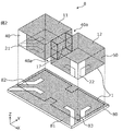
- FIG. 1 is a perspective view showing an example of the structure of a dielectric waveguide filter according to a comparative example of the first embodiment.
- FIG. 2 is an exploded perspective view showing an example of the structure of the high-frequency module according to the comparative example of the first embodiment.
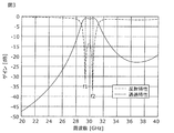
- FIG. 3 is a graph showing an example of frequency characteristics of the dielectric waveguide filter according to the comparative example of the first embodiment.
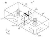
- FIG. 4 is a conceptual diagram illustrating the EVEN mode of the dielectric waveguide filter according to the comparative example of the first embodiment.
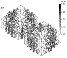
- FIG. 5 is a diagram showing a simulation result of current distribution in the EVEN mode of the dielectric waveguide filter according to the comparative example of the first embodiment.
- FIG. 1 is a perspective view showing an example of the structure of a dielectric waveguide filter according to a comparative example of the first embodiment.
- FIG. 2 is an exploded perspective view showing an example of the structure of the high-frequency module according to the comparative example of the first embodiment.
- FIG. 3 is
- FIG. 6 is a conceptual diagram illustrating the ODD mode of the dielectric waveguide filter according to the comparative example of the first embodiment.
- FIG. 7 is a diagram showing a simulation result of current distribution in the ODD mode of the dielectric waveguide filter according to the comparative example of the first embodiment.
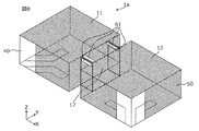
- FIG. 8 is a perspective view showing an example of the structure of the dielectric waveguide filter according to the first embodiment.
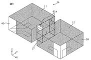
- FIG. 9 is a perspective view showing a construction example of the dielectric exposed portion according to the first embodiment.
- FIG. 10 is a graph showing an example of frequency characteristics of the dielectric waveguide filter according to the first exemplary embodiment.
- FIG. 11 is a perspective view showing an example of the structure of the dielectric waveguide filter according to the first embodiment.
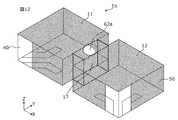
- FIG. 12 is a perspective view showing a construction example of the dielectric exposed portion according to the first embodiment.
- FIG. 13 is a graph showing an example of frequency characteristics of the dielectric waveguide filter according to the first exemplary embodiment.
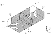
- FIG. 14 is a perspective view showing an example of the structure of a dielectric waveguide filter according to a comparative example of the second embodiment.
- FIG. 15 is an exploded perspective view showing an example of the structure of a high-frequency module according to a comparative example of the second embodiment.
- FIG. 16 is a conceptual diagram illustrating an EVEN mode of a dielectric waveguide filter according to a comparative example of the second embodiment.
- FIG. 17 is a diagram illustrating a simulation result of current distribution in the EVEN mode of the dielectric waveguide filter according to the comparative example of the second embodiment.
- FIG. 18 is a conceptual diagram illustrating an ODD mode of a dielectric waveguide filter according to a comparative example of the second embodiment.
- FIG. 19 is a diagram illustrating a simulation result of current distribution in the ODD mode of the dielectric waveguide filter according to the comparative example of the second embodiment.
- FIG. 20 is a perspective view showing an example of the structure of the dielectric waveguide filter according to the second embodiment.
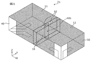
- FIG. 21 is a perspective view showing an example of the structure of the dielectric waveguide filter according to the second embodiment.
- FIG. 22 is a perspective view showing an example of the structure of the dielectric waveguide filter according to the third embodiment.
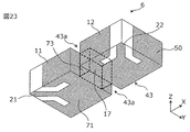
- FIG. 23 is a perspective view showing an example of the structure of a dielectric waveguide filter according to a comparative example of the fourth embodiment.
- FIG. 24 is an exploded perspective view showing an example of the structure of a high-frequency module according to a comparative example of the fourth embodiment.
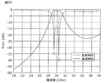
- FIG. 25 is a graph showing an example of frequency characteristics of a dielectric waveguide filter according to a comparative example of the fourth embodiment.
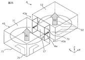
- FIG. 26 is a conceptual diagram illustrating the EVEN mode of the dielectric waveguide filter according to the comparative example of the fourth embodiment.
- FIG. 27A is a perspective view illustrating a simulation result of a magnetic field in the EVEN mode of the dielectric waveguide filter according to the comparative example of the fourth embodiment.
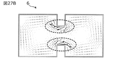
- FIG. 27B is a plan view showing a simulation result of a magnetic field in the EVEN mode of the dielectric waveguide filter according to the comparative example of the fourth embodiment.
- FIG. 28 is a conceptual diagram illustrating an ODD mode of a dielectric waveguide filter according to a comparative example of the fourth embodiment.
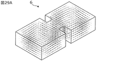
- FIG. 29A is a perspective view showing a simulation result of a magnetic field in the ODD mode of the dielectric waveguide filter according to the comparative example of the fourth embodiment.
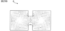
- FIG. 29B is a plan view showing a simulation result of the magnetic field in the ODD mode of the dielectric waveguide filter according to the comparative example of the fourth embodiment.
- FIG. 30 is a perspective view showing an example of the structure of the dielectric waveguide filter according to the fourth embodiment.
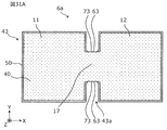
- FIG. 31A is a plan view of a dielectric waveguide filter according to Embodiment 4.
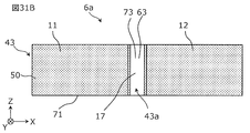
- FIG. 31B is a side view of the dielectric waveguide filter according to the fourth exemplary embodiment.
- FIG. 32 is a plan view showing a simulation result of a magnetic field in the EVEN mode of the dielectric waveguide filter according to the fourth embodiment.
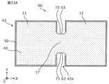
- FIG. 33A is a plan view of a dielectric waveguide filter according to Modification 1 of Embodiment 4.
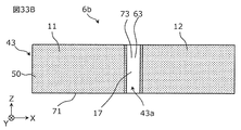
- FIG. FIG. 33B is a side view of a dielectric waveguide filter according to Modification 1 of Embodiment 4.
- FIG. 34 is a plan view showing a simulation result of a magnetic field in the EVEN mode of the dielectric waveguide filter according to the first modification of the sixth embodiment.
- FIG. 35A is a plan view of a dielectric waveguide filter according to Modification 2 of Embodiment 4.
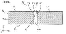
- FIG. FIG. 35B is a side view of the dielectric waveguide filter according to the second modification of the fourth embodiment.
- FIG. 36 is a plan view showing a simulation result of a magnetic field in the EVEN mode of the dielectric waveguide filter according to the second modification of the fourth embodiment.
- FIG. 37 is a diagram illustrating an example of the structure of a dielectric waveguide filter according to a third modification of the fourth embodiment.
- FIG. 38 is a perspective view showing an example of the structure of the dielectric waveguide filter according to the fifth embodiment.
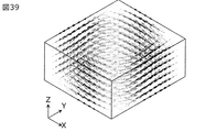
- FIG. 39 is a perspective view showing a simulation result of the magnetic field of the resonating unit according to the fifth embodiment.
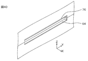
- FIG. 40 is an enlarged perspective view showing an example of the structure of the dielectric waveguide filter according to the fifth embodiment.
- FIG. 41 is a perspective view showing an example of the structure of the dielectric waveguide filter according to the fifth embodiment.
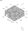
- FIG. 42 is a perspective view showing an example of the structure of a dielectric waveguide filter according to a modification of the fifth embodiment.
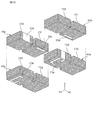
- FIG. 43 is an exploded perspective view showing an example of the structure of a dielectric waveguide filter according to a modification of the fifth embodiment.
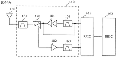
- FIG. 44A is a circuit diagram showing a high-frequency front-end circuit and a communication device according to Embodiment 6.
- FIG. 44B is a circuit diagram showing a high-frequency front end circuit according to Modification 1 of Embodiment 6.
- FIG. 44A is a circuit diagram showing a high-frequency front-end circuit and a communication device according to Embodiment 6.
- FIG. 44B is a circuit diagram showing a high-frequency front end circuit according to Modification 1 of Embodiment 6.
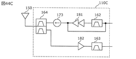
- FIG. 44C is a circuit diagram showing a high-frequency front end circuit according to the second modification of the sixth embodiment.
- FIG. 45A is a circuit diagram showing a Massive MIMO system according to Embodiment 7.
- FIG. 45B is a plan view of the antenna device of the Massive MIMO system according to Embodiment 7.
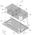
- FIG. 1 is a perspective view showing an example of the structure of a dielectric waveguide filter according to a comparative example of the first embodiment, and shows a general dielectric waveguide filter as viewed from below the mounting surface. Yes.
- the dielectric waveguide filter 1 is composed of a dielectric block 40 having an electrode 50 formed on the surface, and the dielectric block 40 has a groove 40a in a direction crossing the signal propagation direction. Is formed.
- the dielectric block 40 is made of a dielectric material such as crystal or ceramic, and the groove 40a is provided by machining with a wire saw or the like, for example.
- the electrode 50 is formed by, for example, applying and baking a conductive paste containing silver or copper. In FIG. 1, the electrode 50 is disposed in a hatched area on the surface of the dielectric block 40 and is not disposed in a white area.
- the portions not including the groove 40 a are the resonance portions 11 and 12. Further, a portion including the groove 40 a and having a cross section through which a signal can pass is narrower than the resonance portions 11 and 12 is the coupling portion 17.
- the resonating units 11 and 12 generate electromagnetic field resonance inside and function as dielectric resonators.
- the coupling unit 17 couples the resonance units 11 and 12.
- the coupling part 17 is an example of a coupling part constituted by grooves.
- the coupling portion is a portion having a narrow cross section through which a signal can pass as compared with the resonance portion, and is not necessarily constituted by a groove.
- the coupling portion may be configured by a through-hole, a coupling window, or the like, which will be described later.
- the resonance units 11 and 12 are respectively provided with input / output units 21 and 22 for converting a signal propagation mode between a TE (Transverse Electric) mode and a TEM (Transverse ElectroMagnetic) mode.
- the TE mode and the TEM mode are signal propagation modes inside and outside the dielectric waveguide filter 1, respectively.
- the input / output units 21 and 22 are configured by electrodes 50 arranged in a specific shape on the mounting surface of the dielectric waveguide filter 1.
- FIG. 2 is an exploded perspective view showing an example of the structure of the high-frequency module according to the comparative example of the first embodiment.
- the high-frequency module 8 is formed by mounting the dielectric waveguide filter 1 on a substrate 80.
- a broken line on the substrate 80 represents a mounting position of the dielectric waveguide filter 1.
- a conductive foil 81 is laid on the substrate 80.
- the substrate 80 is made of, for example, a resin such as epoxy or phenol, and the conductor foil 81 is made of, for example, a copper foil.
- the conductor foil 81 is disposed in a region indicated by oblique lines on the surface of the substrate 80 and is not disposed in a white region.
- the conductive foil 81 mainly forms a ground plane, and forms coplanar lines 82 and 83 at positions corresponding to the input / output portions 21 and 22 of the dielectric waveguide filter 1.
- the high-frequency module 8 is configured by joining the conductive foil 81 of the substrate 80 and the electrode 50 on the mounting surface of the dielectric waveguide filter 1 with a conductive bonding material such as solder.
- An application circuit using the high frequency module 8 inputs and outputs signals to and from the dielectric waveguide filter 1 via the coplanar lines 82 and 83 of the substrate 80.
- FIG. 3 is a graph showing an example of frequency characteristics of the dielectric waveguide filter 1.
- FIG. 3 shows the simulation results of the reflection characteristics at the input / output unit 21 and the pass characteristics when the input / output unit 21 is viewed from the input / output unit 21.
- the frequency characteristics of the dielectric waveguide filter 1 have notches in the reflection characteristics and peaks in the pass characteristics at the two frequencies f1 and f2. Thereby, the dielectric waveguide filter 1 functions as a bandpass filter having a pass band corresponding to the frequencies f1 and f2.
- the present inventor has found that the respective signals of the frequencies f1 and f2 are coupled by the following different resonance modes. It was.
- FIG. 4 is a diagram for explaining a resonance mode of the dielectric waveguide filter 1 with respect to a signal having a frequency f1.
- the signal of the frequency f1 applied to the input / output unit 21 propagates in the dielectric waveguide filter 1 by exciting the in-phase AC electric fields E1 and E2 in the resonance units 11 and 12. And output from the input / output unit 22.
- a resonance mode in which an in-phase AC electric field is generated between adjacent resonance parts is referred to as an EVEN mode.
- in-phase AC electric fields E1 and E2 are indicated by arrows in the same direction.
- FIG. 5 is a diagram showing a simulation result of current distribution in the EVEN mode of the dielectric waveguide filter 1.
- the EVEN mode current flowing on the surface of the coupling portion 17 becomes dominant in the direction substantially perpendicular to the arrangement direction of the resonance portions 11 and 12 from the side surface to the top surface.
- the top surface is a surface facing the mounting surface on which the dielectric waveguide filter 1 is mounted on the mounting substrate, and the side surface is a surface intersecting the top surface.
- the current I EVEN that becomes dominant in the EVEN mode on the surface of the coupling portion 17 is represented by a thick arrow.
- the current I EVEN is considered to be involved in the coupling of the resonance units 11 and 12.
- FIG. 6 is a diagram for explaining a resonance mode of the dielectric waveguide filter 1 with respect to a signal having a frequency f2.
- the signal having the frequency f2 applied to the input / output unit 21 excites the AC electric fields E1 and E3 having opposite phases to the resonance units 11 and 12, and passes through the dielectric waveguide filter 1. Propagated and output from the input / output unit 22.
- a resonance mode in which an AC electric field having a reverse phase is generated between adjacent resonance parts is referred to as an ODD mode.
- AC electric fields E1 and E3 having opposite phases are represented by arrows pointing in the reverse direction.
- FIG. 7 is a diagram showing a simulation result of current distribution in the ODD mode of the dielectric waveguide filter 1.
- the ODD mode current flowing on the surface of the coupling portion 17 becomes predominant in the direction substantially parallel to the arrangement direction of the resonance portions 11 and 12 near the center of the top surface.
- the current I ODD that prevails in the ODD mode on the surface of the coupling portion 17 is represented by a thick arrow.
- the current I ODD is considered to be involved in the coupling of the resonance units 11 and 12.
- the inventor Based on the analysis result of the current distribution in the dielectric waveguide filter 1 described above, the inventor provides a dielectric exposed portion where the electrode 50 is not formed on a specific portion of the surface of the coupling portion 17, thereby A technique for adjusting the passband width of a body waveguide filter has been devised.
- the dielectric exposed portion is provided on the surface of the coupling portion 17 in a portion where the current density is dominant in any one of the plurality of resonance modes.
- FIG. 8 is a perspective view showing an example of the structure of the dielectric waveguide filter according to the first embodiment.
- the dielectric waveguide filter 1a of FIG. 8 is different from the dielectric waveguide filter 1 of FIG. 1 in that there is a dielectric exposed portion 61 where the electrode 50 is not formed on the surface of the coupling portion 17. .
- the dielectric exposed portion 61 is provided at a position where the current I EVEN in FIG. 4 becomes more dominant than the current I ODD in FIG.
- the dielectric exposed portion 61 is provided in a connection region between the top surface and the side surface of the coupling portion 17.
- the connection region between the top surface and the side surface is a region near the boundary between the top surface and the side surface.
- the top surface is divided into three parts in the direction substantially orthogonal to the signal propagation direction and It may be a region composed of the whole.
- FIG. 9 is a perspective view showing a construction example of the dielectric exposed portion 61.
- the dielectric exposed portion 61 a is formed by cutting the boundary between the top surface and the side surface of the coupling portion 17 with a drill and removing the electrode 50 together with a part of the dielectric block 40. Thus, when forming the dielectric exposure part 61, a part of dielectric block 40 may be shaved.
- the dielectric exposed portion 61 is not limited to drilling, and may be formed by removing only the electrode 50 by laser processing, for example.
- FIG. 10 is a graph showing an example of frequency characteristics of the dielectric waveguide filter 1a.
- FIG. 10 shows simulation results based on the arrangement of the electrodes 50 in FIG. 8 as adjusted reflection characteristics and adjusted pass characteristics. For comparison, the reflection characteristics and transmission characteristics of the dielectric waveguide filter 1 are shown again.
- the frequency of the EVEN mode decreases from f1 to f1a as compared to the frequency characteristic of the dielectric waveguide filter 1, whereas the ODD The mode frequency f2 is generally maintained. Therefore, in the dielectric waveguide filter 1a, the difference between the frequency f1a of the EVEN mode and the frequency f2 of the ODD mode is larger than that of the dielectric waveguide filter 1, and the passband width is expanded (in other words, resonance The coupling between the parts 11 and 12 is strengthened).
- the dielectric exposed portion 61 Since the dielectric exposed portion 61 is provided at a position where the current I EVEN becomes dominant, the dielectric exposed portion 61 strongly inhibits the current I EVEN while not significantly affecting the current I ODD . As a result, it is considered that the current I EVEN must go through a long path, the frequency f1a in the EVEN mode is lowered, and the frequency f2 in the ODD mode is generally maintained.
- the dielectric exposed portion 61 may have a long shape extending substantially parallel to the direction in which the resonance portions 11 and 12 are arranged. As a result, the dielectric exposed portion 61 that is long in the direction intersecting the current I EVEN in FIG. 4 is formed, so that the current I EVEN can be more reliably inhibited and the frequency of the EVEN mode can be more reliably lowered.
- the dielectric exposure portion 61 can selectively adjust the frequency of the EVEN mode to widen the passband width.
- the pass bandwidth can be narrowed with the same concept.
- FIG. 11 is a perspective view showing another example of the structure of the dielectric waveguide filter according to the first embodiment.
- the dielectric waveguide filter 1b of FIG. 11 differs from the dielectric waveguide filter 1a of FIG. 8 in the arrangement of the dielectric exposed portions 62.
- the dielectric exposed portion 62 is provided at a position where the current I ODD in FIG. 5 becomes more dominant than the current I EVEN in FIG.
- the dielectric exposed portion 62 is provided in the central region of the top surface of the coupling portion 17.
- the central region of the top surface may be, for example, a central region obtained by dividing the top surface into three in a direction substantially orthogonal to the signal propagation direction.
- FIG. 12 is a perspective view showing a construction example of the dielectric exposed portion 62.
- the dielectric exposed portion 62 a is formed by cutting the center of the top surface of the coupling portion 17 with a drill and removing the electrode 50 together with a part of the dielectric block 40. As described above, when the dielectric exposed portion 62 is formed, a part of the dielectric block 40 may be removed.
- the dielectric exposed portion 62 is not limited to drilling, and may be formed, for example, by removing only the electrode 50 by laser processing.
- FIG. 13 is a graph showing an example of frequency characteristics of the dielectric waveguide filter 1b.
- FIG. 13 shows simulation results based on the arrangement of the electrodes 50 in FIG. 11 as adjusted reflection characteristics and adjusted pass characteristics. For comparison, the reflection characteristics and transmission characteristics of the dielectric waveguide filter 1 are shown again.
- the frequency of the ODD mode decreases from f2 to f2a as compared with the frequency characteristic of the dielectric waveguide filter 1, whereas EVEN The mode frequency f1 is generally maintained. Therefore, in the dielectric waveguide filter 1b, compared with the dielectric waveguide filter 1, the difference between the frequency f1 of the EVEN mode and the frequency f2a of the ODD mode is reduced, and the passband width is narrowed (in other words, resonance The coupling between the parts 11 and 12 is weakened).
- the dielectric exposed portion 62 Since the dielectric exposed portion 62 is provided at a position where the current I ODD becomes dominant, the dielectric exposed portion 62 strongly inhibits the current I ODD, but does not significantly affect the current I EVEN . As a result, the current I ODD has to go through a long path, the frequency f2a in the ODD mode is lowered, and the frequency f1 in the EVEN mode is generally maintained.
- the dielectric exposed portion 62 may have a long shape extending substantially perpendicular to the direction in which the resonance portions 11 and 12 are arranged. As a result, the dielectric exposed portion 62 that is long in the direction crossing the current I ODD in FIG. 6 is formed, so that the current I ODD can be more reliably inhibited and the frequency of the ODD mode can be lowered more reliably.
- the dielectric exposed portion 62 can selectively adjust the frequency of the ODD mode to narrow the passband width.
- the pass bandwidth of the dielectric waveguide filter is adjusted by adjusting the frequency of a specific resonance mode.
- the adjustment can be performed by simply peeling off a part of the electrode 50 formed on the surface of the coupling portion 17, and it is not essential to change the shape of the dielectric block 40.
- a dielectric waveguide filter can be obtained.
- FIG. 14 is a perspective view showing an example of the structure of a dielectric waveguide filter according to a comparative example of the second embodiment, and shows a general dielectric waveguide filter as viewed from below the mounting surface. Yes.
- the dielectric waveguide filter 2 includes a dielectric block 40 having an electrode 50 formed on the surface, and a through hole 40 b is formed in the dielectric block 40.
- the electrode 50 is arranged in a region indicated by oblique lines on the surface of the dielectric block 40 and is not arranged in a white region. In the dielectric waveguide filter 2, the electrode 50 is also disposed on the inner wall of the through hole 40b.
- the portions not including the through hole 40b are the resonance portions 11 and 12, respectively.
- a portion including the through hole 40 b and having a cross section through which a signal can pass is narrower than the resonance portions 11 and 12 is the coupling portion 18.
- the resonating units 11 and 12 function as a dielectric resonator, and the coupling unit 18 couples the resonating units 11 and 12.
- the coupling portion 18 is an example of a coupling portion configured by a through hole.
- FIG. 15 is an exploded perspective view showing an example of the structure of the high-frequency module according to the comparative example of the second embodiment.
- the high-frequency module 9 is formed by mounting the dielectric waveguide filter 2 on a substrate 80.
- a broken line on the substrate 80 represents a mounting position of the dielectric waveguide filter 2.
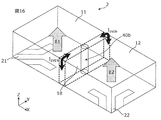
- FIG. 16 is a diagram for explaining the EVEN mode of the dielectric waveguide filter 2. Similar to the EVEN mode of the dielectric waveguide filter 1 described with reference to FIG. 4, the signal applied to the input / output unit 21 excites the in-phase AC electric fields E1 and E2 to the resonance units 11 and 12, thereby causing dielectric conduction. It propagates through the wave tube filter 2 and is output from the input / output unit 22.
- FIG. 17 is a diagram showing a simulation result of current distribution in the EVEN mode of the dielectric waveguide filter 2.
- the current in the EVEN mode flowing through the surface of the coupling portion 18 flows from the side surface to the top surface as seen in the portion surrounded by the dotted line in FIG. 17. In the meantime, it becomes dominant in the direction substantially perpendicular to the direction in which the resonance parts 11 and 12 are arranged.
- the current I EVEN that becomes dominant in the EVEN mode on the surface of the coupling portion 18 is represented by a thick arrow.
- FIG. 18 is a diagram for explaining the ODD mode of the dielectric waveguide filter 2. Similar to the ODD mode of the dielectric waveguide filter 1 described with reference to FIG. 6, the signal applied to the input / output unit 21 excites the AC electric fields E 1 and E 3 having opposite phases to the resonance units 11 and 12, It propagates through the waveguide filter 2 and is output from the input / output unit 22.
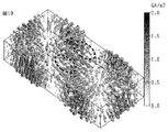
- FIG. 19 is a diagram showing a simulation result of current distribution in the ODD mode of the dielectric waveguide filter 2.
- the current in the ODD mode flowing through the surface of the coupling portion 18 passes through the top surface as seen in the portion surrounded by the dotted line in FIG. On both sides of the mouth of the hole 40b, it becomes dominant in a direction substantially parallel to the direction in which the resonance parts 11 and 12 are arranged.
- the current I ODD that is dominant in the ODD mode on the surface of the coupling portion 18 is represented by a thick arrow.
- a dielectric exposed portion where the electrode 50 is not formed is provided on a specific portion of the surface of the coupling portion 18.
- the pass bandwidth of the dielectric waveguide filter 2 can be adjusted.
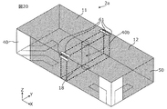
- FIG. 20 is a perspective view showing an example of the structure of the dielectric waveguide filter according to the second embodiment.
- the dielectric waveguide filter 2a in FIG. 20 is different from the dielectric waveguide filter 2 in FIG. 14 in that there is a dielectric exposed portion 61 in which the electrode 50 is not formed on the surface of the coupling portion 18. .
- the dielectric exposed portion 61 is provided at a position where the current I EVEN in FIG. 16 becomes more dominant than the current I ODD in FIG.
- the dielectric exposed portion 61 is provided in a connection region between the top surface and the side surface of the coupling portion 18.
- the connection region between the top surface and the side surface is a region near the boundary between the top surface and the side surface.
- the top surface is divided into three parts in the direction substantially orthogonal to the signal propagation direction and It may be a region composed of the whole.
- the dielectric exposed portion 61 is provided at a position where the current I EVEN dominates, it is considered that the frequency of the EVEN mode is lowered and the frequency of the ODD mode is maintained similarly to the dielectric exposed portion 61.
- the dielectric exposed portion 61 may have a long shape extending substantially parallel to the direction in which the resonance portions 11 and 12 are arranged. Thereby, the long dielectric exposed portion 61 is formed in the direction intersecting with the current I EVEN in FIG. 16, so that the current I EVEN can be more reliably inhibited and the frequency of the EVEN mode can be more reliably lowered.
- the dielectric exposure part 61 can selectively adjust the frequency of the EVEN mode to widen the passband width.
- FIG. 21 is a perspective view showing another example of the structure of the dielectric waveguide filter according to the second embodiment.
- the dielectric waveguide filter 2b shown in FIG. 21 is different from the dielectric waveguide filter 2a shown in FIG.
- the dielectric exposed portion 62 is provided at a position where the current I ODD in FIG. 18 becomes more dominant than the current I EVEN in FIG.
- the dielectric exposed portion 62 is provided in the central region of the top surface of the coupling portion 18.
- the central region of the top surface may be, for example, a region obtained by removing the mouth portion of the through hole 40b from a central region obtained by dividing the top surface into three in a direction substantially orthogonal to the signal propagation direction.
- the dielectric exposed portion 62 is provided at a position where the current I ODD becomes dominant, it is considered that the frequency of the ODD mode is lowered and the frequency of the EVEN mode is maintained, similarly to the dielectric exposed portion 62.
- the dielectric exposed portion 62 may have a long shape extending substantially perpendicular to the direction in which the resonance portions 11 and 12 are arranged. As a result, the dielectric exposed portion 62 that is long in the direction intersecting with the current I ODD in FIG. 18 is formed, so that the current I ODD can be more reliably inhibited and the frequency of the ODD mode can be lowered more reliably.
- the dielectric exposed portion 62 can selectively adjust the frequency of the ODD mode to narrow the passband width.
- the pass bandwidth of the dielectric waveguide filter is adjusted by adjusting the frequency of a specific resonance mode.
- the adjustment can be performed by simply peeling off a part of the electrode 50 formed on the surface of the coupling portion 18, and it is not essential to change the shape of the dielectric block 40.
- FIG. 22 is a perspective view showing an example of the structure of the dielectric waveguide filter according to the third embodiment.
- the dielectric waveguide filter 3 is configured by bonding dielectric waveguide filters 3 a and 3 b provided separately.
- the dielectric waveguide filter 3a is composed of a dielectric block 41 having an electrode 51 formed on the surface thereof, and a groove 41a is formed in the dielectric block 41 in a direction crossing the signal propagation direction (Y direction). Yes.
- the portions not including the groove 41a are the resonance portions 13a, 13b, and 13c.
- the coupling portion 17 is a portion including the groove 41a and having a cross section (XZ plane) through which a signal can pass that is narrower than the XZ cross section of the resonance portions 13a, 13b, and 13c.
- the resonance units 13a, 13b, and 13c function as dielectric resonators, and the coupling unit 17 couples the resonance units 13a and 13b and the resonance units 13b and 13c, respectively.
- the dielectric waveguide filter 3b is composed of a dielectric block 42 having an electrode 52 formed on the surface thereof, and a groove 42a is formed in the dielectric block 42 in a direction crossing the signal propagation direction (Y direction). Yes.
- the portions not including the groove 42a are the resonance portions 13d, 13e, and 13f.
- the coupling portion 17 includes the groove 42a and a cross section (XZ plane) through which a signal can pass is narrower than the XZ cross section of the resonance portions 13d, 13e, and 13f.
- the resonance units 13d, 13e, and 13f function as dielectric resonators, and the coupling unit 17 couples the resonance units 13d and 13e and the resonance units 13e and 13f, respectively.
- a coupling window 53 for coupling the resonating parts 13c and 13d is provided on the joint surface (YZ surface) of the resonating parts 13c and 13d.
- the coupling window 53 is formed by providing portions where the electrodes 51 and 52 are not disposed on the surfaces of the dielectric blocks 41 and 42 facing each other and bonding the portions. Between the resonating parts 13c and 13d, the signal propagates in the X direction, and the coupling window 53 is narrower than the YZ cross section of the resonating parts 13c and 13d.
- a portion not including the coupling window 53 among the plurality of portions obtained by dividing the portions in the signal propagation direction (X direction) is the resonance portion. 13c and 13d. Further, a portion including the coupling window 53 and having a cross section (YZ plane) through which a signal can pass is narrower than the YZ cross section of the resonance portions 13 c and 13 d is the coupling portion 19.
- the coupling portion 19 is an example of a coupling portion configured by a coupling window.
- Dielectric waveguide filters 3a and 3b are bonded to each other with an adhesive, for example, so that dielectric waveguide filter 3 in which resonance portions 13a to 13f are connected in this order is configured.
- FIG. 22 shows an example of the arrangement of the dielectric exposed portions 61 and 62 in each of the coupling portions 17 and 19.
- the dielectric exposed portion 61 is provided in a connection region between the top surface and the side surface of each of the coupling portions 17 and 19.
- the dielectric exposed portion 61 may have an elongated shape that extends substantially parallel to the direction in which adjacent resonance portions are arranged. In FIG. 22, for the sake of simplicity, the dielectric exposed portion 61 is shown only on the top surface of each of the coupling portions 17 and 19.
- the dielectric exposed portion 62 is provided in the central region of the top surface of each of the coupling portions 17 and 19.
- the dielectric exposed portion 62 may have a long shape extending substantially perpendicular to the direction in which the adjacent resonance portions are arranged.
- the pass bandwidth described in the first embodiment can be adjusted by providing any one of the dielectric exposed portions 61 and 62 in each of the coupling portions 17 and 19. it can.
- the passband width is widened (in other words, coupling between adjacent resonance portions is strengthened).
- the dielectric exposed portion 62 is provided, the passband width is narrowed (in other words, the coupling between the adjacent resonance portions is weakened).
- the frequency of the EVEN mode or the ODD mode is selectively adjusted by providing one of the dielectric exposed portions 61 and 62 in each of the coupling portions 17 and 19.
- the pass bandwidth can be adjusted.
- the dielectric exposed portions 61 and 62 provided in the dielectric waveguide filter 3 are confirmed as, for example, drilling marks shown in FIGS. 9 and 12 or laser processing marks (not shown).
- the pass bandwidth of the dielectric waveguide filter is adjusted by adjusting the frequency of a specific resonance mode for each pair of adjacent resonance portions.
- the adjustment can be performed by simply peeling off a part of the electrodes 51 and 52 formed on the surfaces of the coupling portions 17 and 19, and it is not essential to change the shapes of the dielectric blocks 41 and 42.
- FIG. 23 is a perspective view showing an example of the structure of a dielectric waveguide filter according to a comparative example, and shows a general dielectric waveguide filter when the mounting surface 71 is viewed from below.
- the dielectric waveguide filter 6 includes a dielectric block 43 having an electrode 50 formed on the surface thereof.
- the dielectric block 43 has a groove 43a in a direction crossing the signal propagation direction. Is formed.
- the dielectric block 43 is made of, for example, a dielectric material such as crystal or ceramic, and the groove 43a is provided by machining using, for example, a wire saw.
- the electrode 50 is formed by, for example, applying and baking a conductive paste containing silver or copper. In FIG. 23, the electrode 50 is disposed in a region indicated by hatching on the surface of the dielectric block 43 and is not disposed in a white region.
- the portions not including the groove 43 a are the resonance portions 11 and 12. Further, a portion including the groove 43 a and having a cross section through which a signal can pass is narrower than the resonance portions 11 and 12 is the coupling portion 17.
- the resonating units 11 and 12 generate electromagnetic field resonance inside and function as a dielectric resonator in a TE (Transverse Electric) mode.
- the coupling unit 17 couples the resonance units 11 and 12.
- the coupling part 17 is an example of a coupling part constituted by the grooves 43a.
- the resonance units 11 and 12 are provided with input / output units 21 and 22 for converting a signal propagation mode between a TE mode and a TEM (Transverse ElectroMagnetic) mode, respectively.
- the input / output units 21 and 22 are configured by electrodes 50 arranged in a specific shape on the mounting surface 71 of the dielectric waveguide filter 6.
- FIG. 24 is an exploded perspective view showing an example of the structure of the high-frequency module according to the comparative example.
- the high-frequency module 8 is formed by mounting a dielectric waveguide filter 6 on a substrate 80.
- a broken line on the substrate 80 represents a mounting position of the dielectric waveguide filter 6.
- a conductive foil 81 is laid on the substrate 80.
- the substrate 80 is made of, for example, a resin such as epoxy or phenol, and the conductor foil 81 is made of, for example, a copper foil.
- the conductor foil 81 is disposed in a region indicated by oblique lines on the surface of the substrate 80 and is not disposed in a white region.
- the conductive foil 81 mainly constitutes a ground plane, and coplanar lines 82 and 83 are constituted at positions corresponding to the input / output portions 21 and 22 of the dielectric waveguide filter 6.
- the high-frequency module 8 is configured by bonding the conductive foil 81 of the substrate 80 and the electrode 50 on the mounting surface 71 of the dielectric waveguide filter 6 with a conductive bonding material such as solder.
- An application circuit that uses the high-frequency module 8 inputs and outputs signals to and from the dielectric waveguide filter 6 via the coplanar lines 82 and 83 of the substrate 80.
- FIG. 25 is a graph showing an example of frequency characteristics of the dielectric waveguide filter 6.
- FIG. 25 shows respective simulation results of the reflection characteristics at the input / output unit 21 and the transmission characteristics when the input / output unit 22 is viewed from the input / output unit 21.
- the frequency characteristics of the dielectric waveguide filter 6 have notches in the reflection characteristics and peaks in the transmission characteristics at the two resonance frequencies f1 and f2.
- the dielectric waveguide filter 6 functions as a band-pass filter having a pass band corresponding to the resonance frequencies f1 and f2.
- the present inventor has found that the respective resonance frequency f1 and f2 signals are coupled in the following different resonance modes. I found it.
- FIG. 26 is a diagram for explaining a resonance mode of the dielectric waveguide filter 6 with respect to a signal having a resonance frequency f1.
- the signal having the resonance frequency f1 applied to the input / output unit 21 excites the in-phase AC electric fields E1 and E2 in the resonance units 11 and 12, and passes through the dielectric waveguide filter 6. Propagated and output from the input / output unit 22.
- a resonance mode in which an in-phase AC electric field is generated between adjacent resonance parts is referred to as an EVEN mode.
- in-phase AC electric fields E1 and E2 are indicated by arrows in the same direction.
- FIG. 27A is a perspective view showing a simulation result of a magnetic field in the EVEN mode of the dielectric waveguide filter 6.
- FIG. 27B is a plan view showing a simulation result of the magnetic field in the EVEN mode of the dielectric waveguide filter 6, and is a cross section when the dielectric waveguide filter 6 is viewed in plan.
- the EVEN mode magnetic field vector generated in the dielectric waveguide filter 6 appears inside each of the resonance part 11 and the resonance part 12, and in particular, the resonance part. It appears strongly along the side surface 73 of the coupling part 17 that connects 11 and 12.
- the side surface 73 of the coupling portion 17 is a surface that intersects the mounting surface 71 on which the dielectric waveguide filter 6 is mounted on the mounting substrate.
- the magnetic field vector Mv that becomes strong in the EVEN mode of the dielectric waveguide filter 6 is represented by a thick arrow. In the EVEN mode of the dielectric waveguide filter 6, it is considered that the magnetic field vector Mv is involved in the coupling of the resonance units 11 and 12.
- FIG. 28 is a diagram for explaining a resonance mode of the dielectric waveguide filter 6 with respect to a signal having a resonance frequency f2.
- the signal of the resonance frequency f2 applied to the input / output unit 21 excites the AC electric fields E1 and E3 having opposite phases to the resonance units 11 and 12, and the dielectric waveguide filter 6 Is output from the input / output unit 22.
- a resonance mode in which an alternating-phase AC electric field is generated between adjacent resonance parts is referred to as an ODD mode.
- AC electric fields E1 and E3 having opposite phases are represented by arrows pointing in the opposite direction.
- FIG. 29A is a perspective view showing a simulation result of a magnetic field in the ODD mode of the dielectric waveguide filter 6.
- FIG. 29B is a plan view showing a simulation result of the magnetic field in the ODD mode of the dielectric waveguide filter 6, and is a cross section when the dielectric waveguide filter 6 is viewed in plan.
- the ODD mode magnetic field vector generated in the dielectric waveguide filter 6 appears so as to circulate in the opposite directions inside the resonating unit 11 and the resonating unit 12, respectively.
- the magnetic field vector in the ODD mode in the coupling portion 17 appears in a direction substantially perpendicular to the direction in which the resonance portions 11 and 12 are arranged. In the ODD mode of the dielectric waveguide filter 6, it is considered that the magnetic field vector is less likely to be involved in the coupling of the resonance units 11 and 12.
- the present inventor provides a dielectric exposed portion in which the electrode 50 is not formed in a specific portion of the dielectric waveguide filter 6 based on the analysis result of the magnetic field in the dielectric waveguide filter 6 described above.
- a technique for adjusting the passband width of a dielectric waveguide filter has been devised.
- the dielectric exposed portion is provided in a portion where the magnetic field vector strongly appears in the EVEN mode in the dielectric waveguide filter 6.
- FIG. 30 is a perspective view showing an example of the structure of the dielectric waveguide filter 6a according to the sixth embodiment.
- FIG. 31A is a plan view of the dielectric waveguide filter 6a, and is a cross section when the dielectric waveguide filter 6a is viewed in plan.
- FIG. 31B is a side view of the dielectric waveguide filter 6a.
- FIG. 32 is a plan view showing a simulation result of the magnetic field of the dielectric waveguide filter 6a.
- the dielectric waveguide filter 6a of the present embodiment has a dielectric exposed portion 63 where the electrode 50 is not formed on the side surface 73 of the coupling portion 17. It is different in point.
- the dielectric block 43 of the dielectric waveguide filter 6a is provided with a pair of grooves 43a.
- the groove 43 a is provided in the dielectric block 43 so as to have a depth in a direction perpendicular to both the arrangement direction of the resonance parts 11 and 12 and the vertical direction of the mounting surface 71.
- the groove 43 a is provided along a direction perpendicular to the mounting surface 71 and penetrates the dielectric block 43.
- the dielectric exposed portion 63 is provided on the side surface 73 of the coupling portion 17 that is the same surface as the bottom surface of the groove 43a. As described above, the side surface 73 of the coupling portion 17 is a place where the EVEN mode magnetic field vector Mv appears strongly. In the present embodiment, the dielectric exposed portion 63 is provided on the entire side surface 73.
- the dielectric exposed portion 63 is formed by cutting the side surface 73 of the coupling portion 17 with a drill and removing the electrode 50 together with a part of the dielectric block 43. As described above, when the dielectric exposed portion 63 is formed, a part of the dielectric block 43 may be removed.
- the dielectric exposed portion 63 is not limited to drilling, and may be formed by removing only the electrode 50 by laser processing, for example.
- the magnetic field vector Mv is limited by the electrode 50 provided on the side surface 73 of the coupling portion 17.
- the dielectric exposed portion 63 is provided on the side surface 73 of the coupling portion 17, and as shown in FIG. Is alleviated. Therefore, inductive coupling in the EVEN mode can be strengthened.
- the resonance frequency f1 of the EVEN mode is lower than that of the dielectric waveguide filter 6 of the comparative example. Further, the resonance frequency f2 of the ODD mode is generally maintained. Therefore, in the dielectric waveguide filter 6a, compared to the dielectric waveguide filter 6, the difference (f2-f1) in the resonance frequency between the EVEN mode and the ODD mode is increased, and the passband width is widened.
- the passband width of the dielectric waveguide filter 6a can be adjusted by providing the dielectric exposed portion 63 on the side surface 73 of the coupling portion 17. It can.
- the adjustment can be performed by simply peeling off a part of the electrode 50 formed on the side surface 73 of the coupling portion 17, and it is not essential to change the shape of the dielectric block 43.
- it is practically possible to individually adjust the pass bandwidth of many dielectric waveguide filters after the electrodes are formed on the surface in the mass production process.
- a dielectric waveguide filter can be obtained.
- FIG. 33A is a plan view of a dielectric waveguide filter 6b according to Modification 1 of Embodiment 4, and is a cross section when the dielectric waveguide filter 6b is viewed in plan.
- FIG. 33B is a side view of the dielectric waveguide filter 6b.
- FIG. 34 is a plan view showing a simulation result of the magnetic field in the EVEN mode of the dielectric waveguide filter 6b.
- the bottom surface of the groove 43a (side surface 73 of the coupling portion 17) is curved. Specifically, when the groove 43a is viewed in cross section, the bottom surface of the groove 43a is rounded.
- the dielectric exposed portion 63 is provided on the entire bottom surface having the roundness. In other words, when the groove 43 a is viewed in cross section, the dielectric exposed portion 63 is rounded, and a space is formed between both ends of the dielectric exposed portion 63.
- the passband width of the dielectric waveguide filter 6b can be adjusted by providing the dielectric exposed portion 63 on the bottom surface of the groove 43a. Further, since the dielectric exposed portion 63 is rounded, as shown in FIG. 34, a magnetic field vector that penetrates the space from one end portion of both ends of the dielectric exposed portion 63 and reaches the other end portion is obtained. Will occur and inductive coupling can be increased. With this structure, in the dielectric waveguide filter 6b, the passband width can be largely adjusted as compared with the dielectric waveguide filter 6a of the fourth embodiment.
- FIG. 35A is a plan view of a dielectric waveguide filter 6c according to Modification 2 of Embodiment 4, and is a cross section when the dielectric waveguide filter 6c is viewed in plan.
- FIG. 35B is a side view of the dielectric waveguide filter 6c.
- FIG. 36 is a plan view showing a simulation result of a magnetic field in the EVEN mode of the dielectric waveguide filter 6c.
- the dielectric exposed portion 63 is provided not only on the bottom surface of the groove 43a but also on the side surface of the groove 43a. Specifically, the dielectric exposed portion 63 is provided on the opposite side surface 75 of the resonance portions 11 and 12 that is the side surface of the groove 43a.
- the opposing side surface 75 is a surface that intersects the mounting surface 71 and the side surface 73 and faces between the pair of adjacent resonance portions 11 and 12.
- the dielectric exposed portion 63 is U-shaped, and a space is formed between both ends of the dielectric exposed portion 63.
- the passband width of the dielectric waveguide filter 6c is adjusted by providing the dielectric exposed portion 63 on the side surface of the groove 43a (opposite side surface 75 of the resonance portions 11 and 12). can do. Further, since the dielectric exposed portion 63 is provided on the side surface of the groove 43a, as shown in FIG. 36, the dielectric exposed portion 63 penetrates the space from one end portion of the both ends of the dielectric exposed portion 63 to reach the other end portion. A magnetic field vector is generated, and inductive coupling can be increased. With this structure, the passband width of the dielectric waveguide filter 6c can be adjusted larger than that of the dielectric waveguide filter 6a of the fourth embodiment.
- FIG. 37 is a diagram illustrating an example of the structure of the dielectric waveguide filter 6d according to the third modification of the fourth embodiment, and is a cross section when the dielectric waveguide filter 6d is viewed in plan.
- FIG. 37A is an overall view of the dielectric waveguide filter 6d
- FIG. 37B is a partially enlarged view of FIG.
- the dielectric waveguide filter 6d of Modification 3 has four or more continuous resonance portions, and the exposed areas of the dielectric exposure portions 63 provided between adjacent resonance portions are different.
- the dielectric waveguide filter 6d has nine resonating portions 11a, 11b, 11c, 11d, 11e, 11f, 11g, 11h, and 11i.
- the dielectric waveguide filter 6d is composed of a dielectric block 43 having an electrode 50 formed on the surface thereof, and a groove 43a is formed in the dielectric block 43 in a direction crossing the signal propagation direction.
- the portions not including the groove 43a are the resonance portions 11a to 11i.
- a portion including the groove 43a and having a cross section through which a signal can pass is narrower than the resonance portions 11a to 11i is the coupling portion 17.
- the resonating units 11a to 11i cause electromagnetic field resonance inside and function as TE mode dielectric resonators.
- the coupling unit 17 couples the adjacent resonance units 11a to 11i.
- the groove 43a is provided between the adjacent resonance parts 11a to 11i, and the dielectric exposed part 63 is formed in the groove 43a.
- the resonating unit 11a and the resonating unit 11i are provided with input / output units 21 and 22 for converting the signal propagation mode between the TE mode and the TEM mode, respectively.
- the input / output units 21 and 22 are configured by electrodes 50 arranged in a specific shape on the mounting surface 71 of the dielectric waveguide filter 6d.
- the exposed area of the dielectric exposed portion 63 provided on the side surface of the groove 43a differs between adjacent resonators. Specifically, in the arrangement direction of the resonance parts 11a to 11i, the exposed area gradually decreases from one outermost resonance part 11a toward the center resonance part 11e. Further, the exposed area gradually increases from the central resonance portion 11e toward the other outermost resonance portion 11i. For example, as shown in FIG. 37B, the depth of the dielectric exposed portion 63 in the groove 43a between the resonance portions 11a and 11b is d1, and the dielectric exposed portion in the groove 43a between the resonance portions 11b and 11c.
- the depth of the dielectric exposed portion 63 in the groove 43a between the resonance portions 11c and 11d is d3, and the depth of the dielectric exposed portion 63 in the groove 43a between the resonance portions 11d and 11e is d4.
- the exposed area of the dielectric exposed portion 63 of the groove 43a provided between the outermost resonance portion 11a and the resonance portion 11b adjacent to the outermost resonance portion 11a is the outermost resonance portion 11a. Is larger than the exposed area of the dielectric exposed portion 63 of the groove 43a provided between the adjacent resonance portions 11b and 11c. Further, the exposed area of the dielectric exposed portion 63 of the groove 43a provided between the outermost resonance portion 11i and the resonance portion 11h adjacent to the outermost resonance portion 11i is the outermost resonance portion 11i. Is larger than the exposed area of the dielectric exposed portion 63 of the groove 43a provided between the adjacent resonance portions 11h and 11g.
- inductive coupling between the outermost resonance part 11a and the resonance part 11b adjacent to the outermost resonance part 11a is adjacent to the inner side of the outermost resonance part 11a.
- a dielectric waveguide filter 6d having a structure stronger than the inductive coupling between the resonating portions 11b and 11c can be provided.
- the dielectric exposed portion is provided in the portion where the magnetic field of the dielectric waveguide filter strongly appears to adjust the coupling between the adjacent resonance portions.
- the portion where the dielectric exposed portion is provided It is not limited to examples.
- the coupling between the adjacent resonance portions may be adjusted by providing a dielectric exposure portion in a portion where the electric field of the dielectric waveguide filter strongly appears.
- a dielectric waveguide filter in which a plurality of TE mode resonators configured by individual dielectric blocks are coupled, at least one pair of adjacent TE mode resonators has a surface (hereinafter referred to as a maximum electric field).
- a maximum electric field A configuration in which a dielectric exposed portion is provided at the joint of the dielectric block on the surface of the dielectric waveguide filter in the case where they are bonded at a joint surface between them (referred to as E plane).
- FIG. 38 is a perspective view showing an example of the structure of the dielectric waveguide filter according to the fourth embodiment.
- the dielectric waveguide filter 7a is configured by bonding the resonating portions 14a and 14b provided separately.
- the resonating portions 14a and 14b are TE mode resonators configured by dielectric blocks 44a and 44b having electrodes formed on the surfaces, respectively.
- the following magnetic field vectors are generated inside the TE mode resonator, that is, the resonance portions 14a and 14b.
- FIG. 39 is a perspective view showing a simulation result of the magnetic field of the TE mode resonator.
- a magnetic field in the direction along the XY plane appears strongly, so that the electric field becomes maximum on the XY plane.
- the resonating portions 14a and 14b are coupled at the joint surface between the E surfaces where the electric field is maximum.
- the coupling portion that couples the resonating portions 14a and 14b includes a joint surface between the E surfaces that maximizes the electric field.
- a coupling window 54a that couples the resonating portions 14a and 14b is provided at the periphery of the joint surface (XY surface) of the resonating portions 14a and 14b.
- a dielectric exposed portion 64 is provided at the joint 76 of the dielectric blocks 44a and 44b on the surface of the dielectric waveguide filter 7a.
- FIG. 40 is an enlarged perspective view showing an example of a detailed shape of the dielectric exposed portion 64.
- the dielectric exposed portion 64 is formed by, for example, cutting the joint 76 on the surface of the dielectric waveguide filter 7a with a drill and removing the electrodes together with a part of the dielectric blocks 44a and 44b. Is formed by.
- a part of dielectric block 44a, 44b may be shaved. That is, the surfaces of the dielectric blocks 44 a and 44 b may be recessed in the dielectric exposed portion 64.
- the dielectric exposed portion 64 is not limited to drilling, and may be formed by removing only the electrodes by laser processing, for example.
- the position of the coupling window in the dielectric waveguide filter is not limited to the example of FIG.
- FIG. 41 is a perspective view showing an example of the structure of a dielectric waveguide filter in which the installation position of the coupling window is different.
- the dielectric waveguide filter 7b of FIG. 41 is different from the dielectric waveguide filter 7a in that the coupling window 54b is provided at the center of the joint surface (XY plane) of the resonance portions 14a and 14b. Is different.
- the shape of the dielectric exposed portion 64 is the same in the dielectric waveguide filters 7a and 7b.
- the coupling between the resonance parts 14a and 14b in the dielectric waveguide filter 7a is inductive, and the coupling between the resonance parts 14a and 14b in the dielectric waveguide filter 7b is It is capacitive.
- the resonance portion Coupling due to a magnetic field newly occurs between 14a and 14b.
- the main coupling between the resonance parts 14a and 14b is an inductive coupling (for example, the dielectric waveguide filter 7a in FIG. 38)
- the inductive coupling can be strengthened by a newly generated magnetic field.
- the main coupling between the resonating portions 14a and 14b is capacitive coupling (for example, the dielectric waveguide filter 7b in FIG. 41)
- the capacitive coupling can be weakened by a newly generated magnetic field.
- the amount of coupling between the resonance parts can be adjusted after bonding the resonance parts, that is, after manufacturing.
- the coupling by the magnetic field between the resonance portions 14a and 14b is further strengthened through the hollow space, and the coupling adjustment amount is further increased. be able to.
- the mounting direction of the dielectric waveguide filters 7a and 7b to the mounting substrate is not particularly limited.
- the mounting surfaces of the dielectric waveguide filters 7a and 7b may be provided on the XY plane substantially parallel to the joint surfaces of the resonance portions 14a and 14b.
- the resonance portions 14a and 14b are stacked on the mounting substrate, and the bonding surfaces of the resonance portions 14a and 14b are disposed in a direction substantially parallel to the mounting substrate.
- the mounting surfaces of the dielectric waveguide filters 7a and 7b may be provided on the YZ surface or the XZ surface substantially perpendicular to the joint surfaces of the resonance portions 14a and 14b.
- the resonance parts 14a and 14b are arranged in a plane on the mounting board, and the joint surfaces of the resonance parts 14a and 14b are arranged in a direction substantially perpendicular to the mounting board.
- the degree of freedom in mounting and arranging the dielectric waveguide filters 7a and 7b is high.
- the dielectric exposed portion 64 may be provided on the facing surface of the mounting surface of the dielectric waveguide filters 7a and 7b. Thereby, even after the dielectric waveguide filters 7a and 7b are attached to the mounting substrate, the coupling amount between the resonance parts can be easily adjusted.
- FIG. 42 is a perspective view showing an example of the structure of the dielectric waveguide filter according to the first modification of the fifth embodiment.
- FIG. 43 is an exploded perspective view showing an example of the structure of the dielectric waveguide filter according to the first modification of the fifth embodiment.
- the dielectric waveguide filter 7c includes a plurality of resonance units 15a to 15h and input / output units 23a and 23b provided in the resonance units 15a and 15h, respectively.
- the resonance parts 15a, 15b, 15g, and 15h are disposed along the XY plane, and the resonance parts 15d, 15c, 15f, and 15e are respectively disposed on the resonance parts 15a, 15b, 15g, and 15h in the Z direction.
- the XY plane is an example of a predetermined plane
- the Z direction is an example of the vertical direction perpendicular to the predetermined plane.
- the resonating portions 15a and 15b are constituted by a dielectric block 45a and are coupled by a coupling portion constituted by a groove.
- the resonating parts 15c and 15d are constituted by a dielectric block 45b and are coupled by a coupling part constituted by a groove.
- the resonating parts 15e and 15f are constituted by a dielectric block 45c and are coupled by a coupling part constituted by a groove.
- the resonating portions 15g and 15h are constituted by a dielectric block 45d and are coupled by a coupling portion constituted by a groove.
- the resonating parts 15b and 15c are coupled by a coupling part constituted by a coupling window 55a provided in the dielectric blocks 45a and 45b.
- the resonating portions 15d and 15e are coupled by a coupling portion constituted by a coupling window 55b provided in the dielectric blocks 45b and 45c.
- the resonating parts 15f and 15g are coupled by a coupling part constituted by a coupling window 55c provided in the dielectric blocks 45c and 45d.
- the dielectric exposed portions 65a and 65b are provided on the surface of the coupling portion of the resonance portions 15b and 15c, that is, the joint 77 of the dielectric blocks 45a and 45b.
- the dielectric waveguide filter 7c configured as described above, coupling adjustment after manufacture is possible, and a plurality of resonance portions are arranged in the direction along the XY plane and the Z direction perpendicular to the XY plane.
- a compact dielectric waveguide filter in which a large number of resonance parts are arranged in a small area can be obtained.
- FIG. 44A is a circuit diagram showing the high-frequency front-end circuit 110 and its peripheral circuit (communication device) according to the sixth embodiment.
- a high-frequency front-end circuit 110 an antenna element 150, an RF signal processing circuit 191 and a baseband signal processing circuit 192 are shown.
- the high-frequency front end circuit 110 includes filters 161, 162, and 163, a switch circuit 170, a power amplifier circuit 181, and a low noise amplifier circuit 182.
- the power amplifier circuit 181 is a transmission amplification circuit that amplifies the high-frequency transmission signal output from the RF signal processing circuit 191 and outputs the amplified signal to the antenna element 150 via the switch circuit 170 and the filter 161.
- the low noise amplifier circuit 182 is a reception amplification circuit that amplifies a high-frequency signal that has passed through the antenna element 150, the filter 161, and the switch circuit 170 and outputs the amplified signal to the RF signal processing circuit 191.
- the filter 161 is an antenna filter that is connected to the antenna element 150 and selectively allows high-frequency signals in the transmission band and the reception band to pass therethrough, for example.
- the filter 162 is an interstage filter that is disposed between the power amplifier circuit 181 and the RF signal processing circuit 191 and selectively passes a high-frequency signal in the transmission band.
- the filter 163 is an interstage filter that is disposed between the low noise amplifier circuit 182 and the RF signal processing circuit 191 and selectively passes a high frequency signal in the reception band.
- the switch circuit 170 is a switch that switches connection between the antenna element 150 and the transmission signal path and the reception signal path.
- the RF signal processing circuit 191 processes the high-frequency reception signal input from the antenna element 150 via the reception signal path by down-conversion or the like, and the baseband signal processing circuit 192 generates the reception signal generated by the signal processing. Output to.
- the RF signal processing circuit 191 is, for example, an RFIC (Radio Frequency Integrated Circuit). Further, the RF signal processing circuit 191 performs signal processing on the transmission signal input from the baseband signal processing circuit 192 by up-conversion or the like, and outputs the high-frequency transmission signal generated by the signal processing to the power amplifier circuit 181.
- the signal processed by the baseband signal processing circuit 192 is used, for example, for displaying an image as an image signal or for calling as an audio signal.
- the high-frequency front end circuit 110 may include other circuit elements between the filters 161, 162, and 163, the switch circuit 170, the power amplifier circuit 181, and the low noise amplifier circuit 182.
- the dielectric waveguide filters according to the first to fifth embodiments can be used as the filters 161, 162, and 163.
- the pass bandwidths of the filters 161, 162, and 163 can be easily adjusted, so that it is possible to realize a high-frequency front-end circuit that reduces the variation in high-frequency characteristics while reducing the manufacturing cost. .
- FIG. 44B is a circuit diagram showing the high-frequency front-end circuit 110B according to the first modification of the sixth embodiment.
- the high frequency front end circuit 110 ⁇ / b> B includes filters 161, 162 and 163, a power amplifier circuit 181, a low noise amplifier circuit 182, a circulator 171, and a switch circuit 172.
- the high-frequency front end circuit 110B according to this modification is different from the high-frequency front end circuit 110 in the configuration for switching between the transmission signal path and the reception signal path.
- the description of the same configuration as that of the high-frequency front end circuit 110 will be omitted, and a description will be given focusing on different configurations.
- the circulator 171 has an antenna-side terminal, a transmission-side terminal, and a reception-side terminal. During reception, the circulator 171 selectively propagates a reception signal from the antenna element 150 to the reception signal path, and at the time of transmission, the antenna element 150 is transmitted from the transmission signal path. This is a circuit element that selectively propagates a transmission signal to.
- the switch circuit 172 is a switch for switching the connection between the circulator 171 and the reception signal path.
- the receiving side terminal of the circulator 171 is terminated with a terminating resistor (50 ⁇ ).
- the reception side terminal of the circulator 171 is connected to the low noise amplifier circuit 182.
- the high-frequency front end circuit 110B is applied as a time division duplex front-end circuit.
- the dielectric waveguide filters according to the first to fifth embodiments can be used as the filters 161, 162, and 163.
- FIG. 44C is a circuit diagram showing a high-frequency front-end circuit 110C according to the second modification of the sixth embodiment.
- the high frequency front end circuit 110 ⁇ / b> C includes a duplexer 164, filters 162 and 163, a power amplifier circuit 181, a low noise amplifier circuit 182, and an isolator 173.
- the high-frequency front end circuit 110C according to this modification is different from the high-frequency front end circuit 110 in the configuration for switching between the transmission signal path and the reception signal path.
- the description of the same configuration as that of the high-frequency front end circuit 110 will be omitted, and a description will be given focusing on different configurations.
- the duplexer 164 has an antenna terminal, a transmission side terminal, and a reception side terminal, has a transmission filter between the antenna terminal and the transmission side terminal, and has a reception filter between the antenna terminal and the reception side terminal. Have.
- the isolator 173 is a circuit element that is disposed between the transmission-side terminal of the duplexer 164 and the power amplifier circuit 181 and propagates a transmission signal in one direction from the power amplifier circuit 181 to the duplexer 164.
- the isolator 173 can be realized, for example, by terminating one terminal among the three terminals of the circulator by 50 ⁇ .
- the high frequency front end circuit 110C is applied as a front end circuit of a frequency division duplex system.
- the dielectric waveguide filter according to the first to fifth embodiments is used as the transmission-side filter and the reception-side filter of the duplexer 164 and the filters 162 and 163. it can.
- the phantom cell is a network configuration that separates a control signal for ensuring communication stability between a macro cell in a low frequency band and a small cell in a high frequency band and a data signal that is a target of high-speed data communication.
- Each phantom cell is provided with a Massive MIMO antenna device.
- the Massive MIMO system is a technique for improving transmission quality in a millimeter wave band or the like, and controls the directivity of the antenna element by controlling a signal transmitted from each antenna element.
- the Massive MIMO system uses a large number of antenna elements, and therefore can generate a sharp directional beam.
- By increasing the directivity of the beam it is possible to fly radio waves to some extent even in a high frequency band, and it is possible to reduce the interference between cells and increase the frequency utilization efficiency.
- FIG. 45A is a circuit diagram showing a Massive MIMO system according to Embodiment 7.
- FIG. 45B is a plan view of the antenna device of the Massive MIMO system according to Embodiment 7.
- the antenna device 111 shown in FIG. 45B is used in the Massive MIMO system shown in FIG. 45A.
- the antenna device 111 includes a plurality of patch antennas 112 arranged in a matrix.
- FIG. 45A is a diagram illustrating a configuration of a high-frequency front-end circuit 110A including the antenna device 111.
- This high-frequency front end circuit 110A is a Massive MIMO system according to the present embodiment.
- the patch antenna 112 is connected with band-pass filters 161a, 161b and 161c.
- a switch circuit 170a is connected between the filter 161a, the power amplifier circuit 181a, and the low noise amplifier circuit 182a.
- a switch circuit 170b is connected between the filter 161b, the power amplifier circuit 181b, and the low noise amplifier circuit 182b.
- a switch circuit 170c is connected between the filter 161c, the power amplifier circuit 181c, and the low noise amplifier circuit 182c.
- the low noise amplifier circuits 182a, 182b, and 182c are connected to the baseband signal processing circuit 192.
- a band pass filter 162a and a mixer 194a are connected between the baseband signal processing circuit 192 and the power amplifier circuit 181a.
- a band-pass filter 162b and a mixer 194b are connected between the baseband signal processing circuit 192 and the power amplifier circuit 181b.
- a band-pass filter 162c and a mixer 194c are connected between the baseband signal processing circuit 192 and the power amplifier circuit 181c.
- a local oscillator 193 is connected to the mixers 194a, 194b and 194c. The local oscillator 193 outputs, to the mixers 194a to 194c, a reference frequency for up-conversion to a high frequency and down-conversion to a low frequency in the mixers 194a to 194c.
- Filters 161a to 161c pass the transmission / reception frequency band and remove other frequency components.
- the switch circuits 170a to 170c switch between a transmission signal and a reception signal.
- the filters 162a to 162c pass the frequency band of the transmission signal and remove other frequency components.
- the dielectric waveguide filters according to the first to fifth embodiments can be used as the filters 161a to 161c and 162a to 162c.
- the filters 161a to 161c connected to the patch antenna 112 may be arranged on the back surface of the substrate on which the patch antenna 112 is formed. Good. Thereby, the antenna device 111 including the patch antenna 112 with the filters 161a to 161c is configured.
- the pass bandwidths of the filters 161a to 161c and 162a to 162c can be easily adjusted, so that the variation in high-frequency characteristics is reduced while reducing the manufacturing cost.
- a MIMO system can be realized.
- the dielectric waveguide filter, the high-frequency front end circuit, the communication device, and the Massive MIMO system according to the embodiments of the present invention have been described.
- the present invention is not limited to individual embodiments. Unless it deviates from the gist of the present invention, the embodiment in which various modifications conceived by those skilled in the art have been made in the present embodiment, and forms constructed by combining components in different embodiments are also applicable to one or more of the present invention. It may be included within the scope of the embodiments.
- the present invention can be widely used in communication devices such as a millimeter-wave mobile communication system and a Massive MIMO system as a dielectric waveguide filter whose passband width can be easily adjusted.
- Dielectric waveguide filter 8 9 High frequency module 11, 11a to 11i, 12, 13a to 13f, 14a, 14b, 15a to 15h Resonance unit 17 to 19 Coupling unit 21, 22, 23a, 23b Input / output unit 40 to 43, 44a, 44b, 45a to 45d Dielectric block 40a to 43a Groove 40b Through Hole 50 to 52 Electrode 53, 54a, 54b, 55a to 55c Coupling window 61, 61a, 62, 62a, 63, 64, 65a, 65b Dielectric exposed portion 71 Mounting surface 73 Side surface of coupling portion (bottom surface of groove) 75 Opposite side of the resonance part (side of groove) 76, 77 Seam of dielectric block 80 Substrate 81 Conductive foil 82, 83 Coplanar line 110, 110A to 110C High frequency
Landscapes
- Engineering & Computer Science (AREA)
- Computer Networks & Wireless Communication (AREA)
- Signal Processing (AREA)
- Control Of Motors That Do Not Use Commutators (AREA)
Abstract
誘電体導波管フィルタ(1a)は、表面に電極(50)が形成された誘電体ブロック(40)で構成された誘電体導波管フィルタであって、誘電体ブロック(40)は、内部で電磁界の共振が生じる複数の共振部(11、12)と、共振部(11、12)の間に位置し、共振部(11、12)を結合する結合部(17)と、を有し、結合部(17)の表面に、電極(50)が形成されていない誘電体露出部(61)がある。共振部(11、12)は、EVENモードまたはODDモードで共振を生じるTEモードの共振器であってもよく、誘電体露出部(61)は、結合部(17)の何れか1つの共振モードでの結合に関与する部分に設けられる。
Description
本発明は誘電体導波管フィルタ、高周波フロントエンド回路、通信装置、Massive MIMOシステム、及び誘電体導波管フィルタの調整方法に関する。
従来、誘電体共振器の周波数調整について書かれた文献がある(例えば、特許文献1)。特許文献1は、誘電体ブロックに、複数のスリット(溝)により複数の共振部を構成した導波管フィルタを開示している。特許文献1には、スリットの形状(例えば幅や深さ)を用途に応じて変更し、導波管フィルタの電気的結合と帯域幅を制御し、ひいては導波管フィルタの性能特徴を制御できることが記載されている。
しかしながら、上記従来技術においては、誘電体導波管フィルタを製造した後に、通過帯域幅の調整を行うことは困難である。
なぜならば、通過帯域幅を広くするためには、一般に、共振部と共振部との間に形成された溝部の深さを浅くする必要があるが、そもそも誘電体導波管フィルタを製造した後に、溝部の深さを浅くするのは不可能であるからである。
さらに、通過帯域幅を狭くするためには、一般に、共振部と共振部との間に形成された溝部の深さを深くする必要があるが、誘電体導波管フィルタを製造した後では、共振部と共振部との間に形成された溝部には電極が形成されているため、溝部の深さをさらに深くする場合には、削った分の電極を再度形成し直さなくてはならず、工程が複雑になるからである。
そこで、本発明は、誘電体導波管フィルタを製造した後であっても、通過帯域幅の調整が容易な誘電体導波管フィルタ、当該誘電体導波管フィルタを用いた高周波フロントエンド回路、通信装置、Massive MIMOシステム、及び誘電体導波管フィルタの調整方法を提供する。
上記目的を達成するために、本発明の一態様に係る誘電体導波管フィルタは、表面に電極が形成された誘電体ブロックで構成された誘電体導波管フィルタであって、前記誘電体ブロックは、内部で電磁界の共振が生じる複数の共振部と、前記複数の共振部のうち少なくとも1対の隣接する共振部の間に位置し、前記隣接する共振部同士を結合する結合部と、を有し、前記結合部の表面に、前記電極が形成されていない誘電体露出部がある。
誘電体導波管フィルタ内を、TE(Transverse Electric)モードで信号が伝搬するとき、伝搬する信号の周波数に応じて異なる共振モードが生じる。例えば、隣接する共振部に同相の電界が励振されるEVENモード、及び逆相の電界が励振されるODDモードは、異なる共振モードの一例である。誘電体導波管フィルタの通過帯域幅は、異なる複数の共振モードの合成により得られる。
そこで、上述の構成により、誘電体ブロックの結合部の表面に、誘電体露出部を設ける。誘電体露出部を、複数の共振モードのうち何れか1つの共振モードの結合に関与する部分に設けることで、当該共振モードの周波数が下がる。このようにして、特定の共振モードの周波数を調整することで、誘電体導波管フィルタの通過帯域幅が調整される。
当該調整は、誘電体ブロックの結合部の表面に形成された電極の一部を単に剥がすだけで行うことができ、誘電体ブロックの形状を変更することは必須ではない。その結果、通過帯域幅の調整が容易な誘電体導波管フィルタが得られる。
また、前記誘電体露出部は、前記結合部の表面のうち、前記誘電体導波管フィルタが実装基板に実装される実装面と対向する天面と、前記天面と交差する側面と、の接続領域に形成されていてもよい。
この構成によれば、前述したEVENモード及びODDモードのうち、EVENモードでの結合に関与する電流の密度が優勢になる部分に誘電体露出部が形成されるので、EVENモードの周波数を下げつつ、ODDモードの周波数を維持できる。その結果、例えば、EVENモードの周波数がODDモードの周波数より低い場合、EVENモードの周波数とODDモードの周波数との差が大きくなり、誘電体導波管フィルタの帯域幅を広げる(言い換えれば、結合を強める)ことができる。
また、前記誘電体露出部は、前記共振部の並び方向と略平行に延びる長尺形状であってもよい。
この構成によれば、EVENモードで優勢となる電流と交差する方向に長い誘電体露出部を形成するので、EVENモードの周波数をより確実に下げることができる。
また、前記誘電体露出部は、前記結合部の表面のうち、前記誘電体導波管フィルタが実装基板に実装される実装面と対向する天面の中央領域に形成されていてもよい。
この構成によれば、前述したEVENモード及びODDモードのうち、ODDモードでの結合に関与する電流の密度が優勢になる部分に誘電体露出部が形成されるので、ODDモードの周波数を下げつつ、EVENモードの周波数を維持できる。その結果、例えば、EVENモードの周波数がODDモードの周波数より低い場合、EVENモードの周波数とODDモードの周波数との差が小さくなり、誘電体導波管フィルタの帯域幅を狭める(言い換えれば、結合を弱める)ことができる。
また、前記誘電体露出部は、前記共振部の並び方向と略垂直に延びる長尺形状であってもよい。
この構成によれば、ODDモードで優勢となる電流と交差する方向に長い誘電体露出部を形成するので、ODDモードの周波数をより確実に下げることができる。
また、前記誘電体ブロックは、溝、貫通孔、及び結合窓のうち少なくとも1つを有し、前記誘電体ブロックを信号の伝搬方向に区分した複数の部分のうち、前記溝、前記貫通孔、及び前記結合窓の何れも有しない部分が前記共振部であり、前記溝、前記貫通孔、及び前記結合窓のうち少なくとも前記1つによって、前記共振部と比べて信号が通過可能な断面が狭められた部分が前記結合部であってもよい。
この構成によれば、溝、貫通孔、及び結合窓により、誘電体ブロックに共振部と結合部とを設けることができる。
また、前記結合部は、前記誘電体導波管フィルタが実装基板に実装される実装面と交差する側面を有し、前記複数の共振部のそれぞれは、TEモードの共振器であり、前記実装面及び前記側面に交差し、かつ、前記1対の隣接する共振部の間にて向き合う対向側面を有し、前記誘電体露出部は、前記結合部の前記側面及び前記共振部の前記対向側面のうち少なくとも一方に設けられていてもよい。
この構成によれば、EVENモードでの誘導性結合が強くなる部分に誘電体露出部が形成されるので、EVENモードの共振周波数を下げつつ、ODDモードの共振周波数を維持できる。その結果、例えば、EVENモードの共振周波数がODDモードの共振周波数より低い場合、EVENモードの共振周波数とODDモードの共振周波数との差が大きくなり、誘電体導波管フィルタの帯域幅を広げることができる。
また、前記誘電体露出部は、前記結合部の前記側面に設けられていてもよい。
この構成によれば、誘導性結合が強くなる結合部の側面に誘電体露出部を形成するので、EVENモードの共振周波数をより確実に下げることができる。
また、前記誘電体露出部は、前記結合部の前記側面及び前記共振部の前記対向側面の両方に設けられていてもよい。
この構成によれば、誘導性結合が強くなる結合部の側面及び共振部の対向側面に誘電体露出部を形成するので、EVENモードの共振周波数をより確実に下げることができる。
また、前記誘電体ブロックには、前記共振部の並び方向及び前記実装面の垂直方向の両方に垂直な方向に深さを有する溝が設けられ、前記誘電体ブロックを信号の伝搬方向に区分した複数の部分のうち、前記溝を有しない部分が前記共振部であり、前記溝によって、前記共振部と比べて信号が通過可能な断面が狭められた部分が前記結合部であり、前記溝の底面は、前記結合部の前記側面であり、前記溝の側面は、前記共振部の前記対向側面であってもよい。
この構成によれば、上記溝により、誘電体ブロックに共振部の対向側面と結合部の側面とを設けることができる。
また、前記溝の前記底面は、前記溝を断面視した場合に丸みを有していてもよい。
この構成によれば、誘導性結合が強くなる部分である結合部の側面の露出面積を大きくすることができるので、EVENモードの共振周波数をより確実に下げることができる。
また、前記誘電体露出部は、前記溝の前記底面の全てに設けられていてもよい。
この構成によれば、誘導性結合が強くなる部分である結合部の側面の全部に誘電体露出部を形成するので、EVENモードの共振周波数をより確実に下げることができる。
また、前記誘電体ブロックは、4以上の連なる前記共振部を備え、前記隣接する共振部の間のそれぞれには、前記誘電体露出部が形成された前記溝が設けられ、4以上の連なる前記共振部のうち、最外端の共振部と前記最外端の共振部に隣接する共振部との間に設けられた前記溝の前記誘電体露出部の露出面積は、前記最外端の共振部の内側にて隣接する共振部同士の間に設けられた前記溝の前記誘電体露出部の露出面積よりも大きくてもよい。
この構成によれば、最外端の共振部と最外端の共振部に隣接する共振部との誘導性結合が、最外端の共振部の内側にて隣接する共振部同士の誘導性結合よりも強い誘電体導波管フィルタを提供することができる。
前記複数の共振部のそれぞれは、個別の誘電体ブロックで構成されたTEモードの共振器であり、前記結合部は、前記1対の隣接する共振部の電界最大となる面同士の接合面を含み、前記誘電体露出部は、前記誘電体導波管フィルタの表面の前記誘電体ブロックの継ぎ目に設けられていてもよい。
この構成によれば、電界最大となる面でTEモード共振器を結合させた誘電体フィルタにおいて、TEモード共振器の接合面の端部に電極が形成されない誘電体露出部を設けている。これにより、共振部間に磁界による結合が新たに発生する。そのため隣接する共振部の主結合が容量性結合の場合、新たに発生した磁界結合によりこれを打ち消し弱めることができ、また主結合が誘導性結合の場合は、これを強めることができる。この調整は、共振部を張り合わせた後、すなわち誘電体導波管フィルタの製造後に行うことができる。
前記複数の共振部は、所定平面に沿って配置された複数の第1共振部を含む第1共振部群と、前記所定平面に垂直な上下方向において、前記第1共振部群上に配置された1以上の第2共振部を含む第2共振部群と、を含み、前記上下方向に配置された前記第1共振部と前記第2共振部とは、電界最大となる面同士の接合面を含む結合部にて結合し、前記誘電体露出部は、前記第1共振部と前記第2共振部との結合部の表面に設けられていてもよい。
この構成によれば、製造後の結合調整が可能で、かつ所定平面に沿った方向および垂直な方向に複数の共振部を配置することで小面積に多数の共振部を配置したコンパクトな誘電体導波管フィルタが得られる。
前記接合面は、前記誘電体導波管フィルタの実装面と略平行に設けられていてもよい。また、前記接合面は、前記誘電体導波管フィルタの実装面と略垂直に設けられていてもよい。
これらの構成によれば、製造後の結合調整が可能で、かつ実装配置の自由度が高い誘電体導波管フィルタが得られる。
前記誘電体ブロックの表面は、前記誘電体露出部において窪んでいてもよい。
この構成によれば、隣接する共振部間の磁界による結合が、窪んだ中空の空間を通してさらに強くなり、結合調整量をさらに大きくすることができる。
本発明の一態様に係る高周波フロントエンド回路は、アンテナ素子に接続された、前述の誘電体導波管フィルタと、前記アンテナ素子へ送信する高周波送信信号を増幅する送信増幅回路と、前記アンテナ素子で受信した高周波受信信号を増幅する受信増幅回路と、前記送信増幅回路及び前記受信増幅回路と、前記誘電体導波管フィルタとの接続を切り替えるスイッチ回路と、を備える。
本発明の一態様に係る高周波フロントエンド回路は、RF信号処理回路から出力される高周波送信信号を増幅する送信増幅回路と、高周波受信信号を増幅して前記RF信号処理回路へ出力する受信増幅回路と、前記RF信号処理回路と前記送信増幅回路との間、又は、前記RF信号処理回路と前記受信増幅回路との間に配置された、前述の誘電体導波管フィルタと、を備える。
これらの構成によれば、前述の誘電体導波管フィルタの特徴である、通過帯域幅の調整が容易な高周波フロントエンド回路が得られる。
本発明の一態様に係る通信装置は、アンテナ素子と、前記アンテナ素子に接続され、前記アンテナ素子で送信及び受信される高周波信号を増幅する、前述の高周波フロントエンド回路と、前記高周波フロントエンド回路に接続され、前記高周波信号とベースバンド信号との間の周波数変換を含む信号処理を行うRF信号処理回路と、前記RF信号処理回路に接続され、前記ベースバンド信号を信号処理するベースバンド信号処理回路と、を備える。
この構成によれば、前述の高周波フロントエンド回路が備える誘電体導波管フィルタの特徴である、通過帯域幅の調整が容易な通信装置が得られる。
本発明の一態様に係るMassive MIMOシステムは、行列状に配列された複数のパッチアンテナを含むアンテナと、パッチアンテナごとに前述の誘電体導波管フィルタと、を備える。
この構成によれば、前述の誘電体導波管フィルタの特徴である、通過帯域幅の調整が容易なMassive MIMOシステムが得られる。
本発明の一態様に係る誘電体導波管フィルタの調整方法は、表面に電極が形成された誘電体ブロックで構成され、前記誘電体ブロックは、内部で電磁界の共振が生じる複数の共振部と、隣接する共振部の間に位置し、隣接する共振部同士を結合する結合部と、を有する誘電体導波管フィルタにおいて、前記結合部の表面に形成された前記電極の一部を除去するものである。
この方法によれば、必ずしも誘電体ブロックの形状を変更しなくても、誘電体ブロックの結合部の表面に形成された電極の一部を単に剥がすだけで、容易に、誘電体導波管フィルタの周波数と帯域幅とを調整することができる。
本発明によれば、誘電体導波管フィルタを製造した後であっても、通過帯域幅の調整が容易な誘電体導波管フィルタ、当該誘電体導波管フィルタを用いた高周波フロントエンド回路、通信装置、Massive MIMOシステム、及び当該誘電体導波管フィルタの調整方法が得られる。
(本発明の一態様を得るに至った第1の経緯)
本発明の一態様を得るに至った第1の経緯について説明する。第1の経緯では、実施の形態1について説明する前に、本発明者が検討した一般的な誘電体導波管フィルタの構造及び周波数特性を、実施の形態1の比較例として説明する。
本発明の一態様を得るに至った第1の経緯について説明する。第1の経緯では、実施の形態1について説明する前に、本発明者が検討した一般的な誘電体導波管フィルタの構造及び周波数特性を、実施の形態1の比較例として説明する。
図1は、実施の形態1の比較例に係る誘電体導波管フィルタの構造の一例を示す斜視図であり、一般的な誘電体導波管フィルタを、実装面を下から見て示している。図1に示されるように、誘電体導波管フィルタ1は、表面に電極50が形成された誘電体ブロック40で構成され、誘電体ブロック40には信号の伝搬方向と交差する方向に溝40aが形成されている。
誘電体ブロック40は、例えば、水晶又はセラミックなどの誘電体材料で構成され、溝40aは、例えば、ワイヤソーなどによる機械加工により設けられる。電極50は、例えば、銀又は銅を含有する導電性ペーストの塗布、焼成により形成される。電極50は、図1において、誘電体ブロック40の表面の斜線で示した領域に配置され、白抜きの領域には配置されていない。
誘電体ブロック40を信号の伝搬方向に区分した複数の部分のうち、溝40aを含まない部分が共振部11、12である。また、溝40aを含み、信号が通過可能な断面が共振部11、12より狭い部分が結合部17である。共振部11、12は、内部で電磁界の共振を生じ、誘電体共振器として機能する。結合部17は、共振部11、12を結合する。結合部17は、溝によって構成された結合部の一例である。
なお、本明細書において、結合部は、共振部と比べて、信号が通過可能な断面が狭い部分であり、必ずしも溝によって構成されるとは限らない。結合部は、例えば、後述する貫通孔、結合窓などによって構成されてもよい。
共振部11、12には、信号の伝搬モードをTE(Transverse Electric)モードとTEM(Transverse ElectroMagnetic)モードとの間で変換する入出力部21、22が、それぞれ設けられている。ここで、TEモード及びTEMモードは、それぞれ、誘電体導波管フィルタ1の内部及び外部での信号の伝搬モードである。入出力部21、22は、誘電体導波管フィルタ1の実装面に、特定の形状で配置された電極50によって、構成される。
図2は、実施の形態1の比較例に係る高周波モジュールの構造の一例を示す分解斜視図である。図2に示されるように、高周波モジュール8は、誘電体導波管フィルタ1を基板80に実装してなる。基板80の破線は、誘電体導波管フィルタ1の実装位置を表している。
基板80には、導体箔81が敷設される。基板80は、例えば、エポキシ、フェノールなどの樹脂で構成され、導体箔81は、例えば、銅箔などで構成される。導体箔81は、図2において、基板80の表面の斜線で示した領域に配置され、白抜きの領域には配置されていない。
導体箔81は、主にグランドプレーンを構成し、誘電体導波管フィルタ1の入出力部21、22の対応位置では、コプレーナライン82、83を構成している。
基板80の導体箔81と誘電体導波管フィルタ1の実装面における電極50とを、はんだなどの導電性接合材で接合して、高周波モジュール8は構成される。高周波モジュール8を利用する応用回路は、基板80のコプレーナライン82、83を介して、誘電体導波管フィルタ1に信号を入出力する。
図3は、誘電体導波管フィルタ1の周波数特性の一例を示すグラフである。図3には、入出力部21における反射特性、及び入出力部21から入出力部22を見た通過特性の、それぞれのシミュレーション結果が示されている。
図3に示されるように、誘電体導波管フィルタ1の周波数特性は、2つの周波数f1、f2において、反射特性にノッチを有し通過特性にピークを有する。これにより、誘電体導波管フィルタ1は、周波数f1、f2に応じた通過帯域を有するバンドパスフィルタとして機能する。
本発明者は、シミュレーションにより誘電体導波管フィルタ1の電磁界解析を行った結果、周波数f1、f2のそれぞれの信号に対し、次のような異なる共振モードによる結合が生じていることを見出した。
図4は、周波数f1の信号に対する誘電体導波管フィルタ1の共振モードを説明する図である。図4に示されるように、入出力部21に印加された周波数f1の信号は、共振部11、12に同相の交流電界E1、E2を励振して、誘電体導波管フィルタ1内を伝搬し、入出力部22から出力される。本明細書では、隣接する共振部間に同相の交流電界が生じる共振モードをEVENモードと言う。図4では、同相の交流電界E1、E2を同じ向きの矢印で表している。
図5は、誘電体導波管フィルタ1のEVENモードにおける電流分布のシミュレーション結果を示す図である。図5の点線で囲んだ部分に見られるように、結合部17の表面を流れるEVENモードの電流は、側面から天面にかけて共振部11、12の並び方向と略垂直な方向に優勢となる。ここで、天面とは、誘電体導波管フィルタ1が実装基板に実装される実装面と対向する面であり、側面とは、天面と交差する面である。図4では、結合部17の表面においてEVENモードで優勢となる電流IEVENを太矢印で表している。誘電体導波管フィルタ1のEVENモードでは、電流IEVENが共振部11、12の結合に関与していると考えられる。
図6は、周波数f2の信号に対する誘電体導波管フィルタ1の共振モードを説明する図である。図6に示されるように、入出力部21に印加された周波数f2の信号は、共振部11、12に逆相の交流電界E1、E3を励振して、誘電体導波管フィルタ1内を伝搬し、入出力部22から出力される。本明細書では、隣接する共振部間に逆相の交流電界が生じる共振モードをODDモードと言う。図6では、逆相の交流電界E1、E3を逆向きの矢印で表している。
図7は、誘電体導波管フィルタ1のODDモードにおける電流分布のシミュレーション結果を示す図である。図7の点線で囲んだ部分に見られるように、結合部17の表面を流れるODDモードの電流は、天面の中央付近で共振部11、12の並び方向と略平行な方向に優勢となる。図6では、結合部17の表面においてODDモードで優勢となる電流IODDを太矢印で表している。誘電体導波管フィルタ1のODDモードでは、電流IODDが共振部11、12の結合に関与していると考えられる。
本発明者は、上述した誘電体導波管フィルタ1における電流分布の分析結果に基づき、結合部17の表面の特定の部分に電極50が形成されていない誘電体露出部を設けることで、誘電体導波管フィルタの通過帯域幅を調整する技術を考案した。誘電体露出部は、結合部17の表面において複数の共振モードのうち何れか1つの共振モードで電流密度が優勢になる部分に設けられる。
以下、本発明の実施の形態に係る誘電体導波管フィルタについて、図面を用いて詳細に説明する。なお、以下で説明する実施の形態は、いずれも包括的又は具体的な例を示すものである。以下の実施の形態で示される数値、形状、材料、構成要素、構成要素の配置および接続形態などは、一例であり、本発明を限定する主旨ではない。以下の実施の形態における構成要素のうち、独立請求項に記載されていない構成要素については、任意の構成要素として説明される。また、図面に示される構成要素の大きさ又は大きさの比は、必ずしも厳密ではない。
(実施の形態1)
図8は、実施の形態1に係る誘電体導波管フィルタの構造の一例を示す斜視図である。図8の誘電体導波管フィルタ1aは、図1の誘電体導波管フィルタ1と比べて、結合部17の表面に、電極50が形成されていない誘電体露出部61がある点が異なる。
図8は、実施の形態1に係る誘電体導波管フィルタの構造の一例を示す斜視図である。図8の誘電体導波管フィルタ1aは、図1の誘電体導波管フィルタ1と比べて、結合部17の表面に、電極50が形成されていない誘電体露出部61がある点が異なる。
誘電体露出部61は、図4の電流IEVENが、図5の電流IODDと比べて、より優勢になる位置に設けられる。一例として、誘電体露出部61は、結合部17の天面と側面との接続領域に設けられる。ここで、天面と側面との接続領域とは、天面と側面との境界の近傍領域であり、例えば、天面を信号の伝搬方向と略直交する方向に3分割した両端部分と側面の全体とからなる領域であってもよい。
図9は、誘電体露出部61の施工例を示す斜視図である。誘電体露出部61aは、結合部17の天面と側面との境界をドリルで切削し、電極50を誘電体ブロック40の一部とともに除去することによって形成されている。このように、誘電体露出部61を形成する際、誘電体ブロック40の一部が削れても構わない。なお、誘電体露出部61は、ドリル加工に限らず、例えば、レーザー加工により電極50のみを除去することによって形成されてもよい。
図10は、誘電体導波管フィルタ1aの周波数特性の一例を示すグラフである。図10には、図8の電極50の配置に基づくシミュレーション結果を、調整後反射特性及び調整後通過特性として示している。また、比較のため、誘電体導波管フィルタ1の反射特性及び通過特性を再掲している。
図10に示されるように、誘電体導波管フィルタ1aの周波数特性では、誘電体導波管フィルタ1の周波数特性と比べて、EVENモードの周波数がf1からf1aへ低下するのに対し、ODDモードの周波数f2は概ね維持される。そのため、誘電体導波管フィルタ1aでは、誘電体導波管フィルタ1と比べて、EVENモードの周波数f1aとODDモードの周波数f2との差が大きくなり、通過帯域幅が広がる(言い換えれば、共振部11、12間の結合が強まる)。
誘電体露出部61は、電流IEVENが優勢になる位置に設けられるため、電流IEVENを強く阻害する一方で、電流IODDには大きな影響を与えない。その結果、電流IEVENは長い経路を通らざるを得なくなってEVENモードの周波数f1aは下がり、ODDモードの周波数f2は概ね維持されると考えられる。
誘電体露出部61は、図8に示されるように、共振部11、12の並び方向と略平行に延びる長尺形状であってもよい。これにより、図4の電流IEVENと交差する方向に長い誘電体露出部61が形成されるので、電流IEVENをより確実に阻害し、EVENモードの周波数をより確実に下げることができる。
このように、誘電体導波管フィルタ1aでは、誘電体露出部61により、EVENモードの周波数を選択的に調整し、通過帯域幅を広げることができる。
同様の考え方で、通過帯域幅を狭めることもできる。
図11は、実施の形態1に係る誘電体導波管フィルタの構造の他の一例を示す斜視図である。図11の誘電体導波管フィルタ1bは、図8の誘電体導波管フィルタ1aと比べて、誘電体露出部62の配置が異なる。
誘電体露出部62は、図5の電流IODDが、図4の電流IEVENと比べて、より優勢になる位置に設けられる。一例として、誘電体露出部62は、結合部17の天面の中央領域に設けられる。ここで、天面の中央領域とは、例えば、天面を信号の伝搬方向と略直交する方向に3分割した中央の領域であってもよい。
図12は、誘電体露出部62の施工例を示す斜視図である。誘電体露出部62aは、結合部17の天面の中央をドリルで切削し、電極50を誘電体ブロック40の一部とともに除去することによって形成されている。このように、誘電体露出部62を形成する際、誘電体ブロック40の一部が削れても構わない。なお、誘電体露出部62は、ドリル加工に限らず、例えば、レーザー加工により電極50のみを除去することによって形成されてもよい。
図13は、誘電体導波管フィルタ1bの周波数特性の一例を示すグラフである。図13には、図11の電極50の配置に基づくシミュレーション結果を、調整後反射特性及び調整後通過特性として示している。また、比較のため、誘電体導波管フィルタ1の反射特性及び通過特性を再掲している。
図13に示されるように、誘電体導波管フィルタ1bの周波数特性では、誘電体導波管フィルタ1の周波数特性と比べて、ODDモードの周波数がf2からf2aへ低下するのに対し、EVENモードの周波数f1は概ね維持される。そのため、誘電体導波管フィルタ1bでは、誘電体導波管フィルタ1と比べて、EVENモードの周波数f1とODDモードの周波数f2aとの差が小さくなり、通過帯域幅が狭まる(言い換えれば、共振部11、12間の結合が弱まる)。
誘電体露出部62は、電流IODDが優勢になる位置に設けられるため、電流IODDを強く阻害する一方で、電流IEVENには大きな影響を与えない。その結果、電流IODDは長い経路を通らざるを得なくなってODDモードの周波数f2aは下がり、EVENモードの周波数f1は概ね維持されると考えられる。
誘電体露出部62は、図11に示されるように、共振部11、12の並び方向と略垂直に延びる長尺形状であってもよい。これにより、図6の電流IODDと交差する方向に長い誘電体露出部62が形成されるので、電流IODDをより確実に阻害し、ODDモードの周波数をより確実に下げることができる。
このように、誘電体導波管フィルタ1bでは、誘電体露出部62により、ODDモードの周波数を選択的に調整し、通過帯域幅を狭めることができる。
以上説明したように、誘電体導波管フィルタ1a、1bによれば、特定の共振モードの周波数を調整することで、誘電体導波管フィルタの通過帯域幅が調整される。当該調整は、結合部17の表面に形成された電極50の一部を単に剥がすだけで行うことができ、誘電体ブロック40の形状を変更することは必須ではない。その結果、例えば、量産工程で表面に電極を形成した後の多数の誘電体導波管フィルタの通過帯域幅を個別に調整することが実際的に可能になるなど、通過帯域幅の調整が容易な誘電体導波管フィルタが得られる。
(実施の形態2)
実施の形態2では、誘電体ブロックに設けられた貫通孔によって共振部と結合部とが規定される誘電体導波管フィルタにおける通過帯域幅の調整について説明する。
実施の形態2では、誘電体ブロックに設けられた貫通孔によって共振部と結合部とが規定される誘電体導波管フィルタにおける通過帯域幅の調整について説明する。
図14は、実施の形態2の比較例に係る誘電体導波管フィルタの構造の一例を示す斜視図であり、一般的な誘電体導波管フィルタを、実装面を下から見て示している。図14に示されるように、誘電体導波管フィルタ2は、表面に電極50が形成された誘電体ブロック40で構成され、誘電体ブロック40には貫通孔40bが形成されている。
電極50は、図14において、誘電体ブロック40の表面の斜線で示した領域に配置され、白抜きの領域には配置されていない。誘電体導波管フィルタ2では、電極50は、貫通孔40bの内壁にも配置されている。
誘電体ブロック40を信号の伝搬方向に区分した複数の部分のうち、貫通孔40bを含まない部分が、共振部11、12である。また、貫通孔40bを含み、信号が通過可能な断面が共振部11、12より狭い部分が結合部18である。共振部11、12は、誘電体共振器として機能し、結合部18は、共振部11、12を結合する。結合部18は、貫通孔によって構成された結合部の一例である。
図15は、実施の形態2の比較例に係る高周波モジュールの構造の一例を示す分解斜視図である。図15に示されるように、高周波モジュール9は、誘電体導波管フィルタ2を基板80に実装してなる。基板80の破線は、誘電体導波管フィルタ2の実装位置を表している。
図16は、誘電体導波管フィルタ2のEVENモードを説明する図である。図4で説明した誘電体導波管フィルタ1のEVENモードと同様、入出力部21に印加された信号は、共振部11、12に同相の交流電界E1、E2を励振して、誘電体導波管フィルタ2内を伝搬し、入出力部22から出力される。
図17は、誘電体導波管フィルタ2のEVENモードにおける電流分布のシミュレーション結果を示す図である。図5の誘電体導波管フィルタ1のEVENモードほど明確ではないが、図17の点線で囲んだ部分に見られるように、結合部18の表面を流れるEVENモードの電流は、側面から天面にかけて共振部11、12の並び方向と略垂直な方向に優勢となる。図16では、結合部18の表面においてEVENモードで優勢となる電流IEVENを太矢印で表している。
図18は、誘電体導波管フィルタ2のODDモードを説明する図である。図6で説明した誘電体導波管フィルタ1のODDモードと同様、入出力部21に印加された信号は、共振部11、12に逆相の交流電界E1、E3を励振して、誘電体導波管フィルタ2内を伝搬し、入出力部22から出力される。
図19は、誘電体導波管フィルタ2のODDモードにおける電流分布のシミュレーション結果を示す図である。図7の誘電体導波管フィルタ1のODDモードほど明確ではないが、図19の点線で囲んだ部分に見られるように、結合部18の表面を流れるODDモードの電流は、天面の貫通孔40bの口部の両側で共振部11、12の並び方向と略平行な方向に優勢となる。図18では、結合部18の表面においてODDモードで優勢となる電流IODDを太矢印で表している。
誘電体導波管フィルタ2における電流分布の分析に基づき、誘電体導波管フィルタ1の場合と同様、結合部18の表面の特定の部分に電極50が形成されていない誘電体露出部を設けることで、誘電体導波管フィルタ2の通過帯域幅を調整することができる。
図20は、実施の形態2に係る誘電体導波管フィルタの構造の一例を示す斜視図である。図20の誘電体導波管フィルタ2aは、図14の誘電体導波管フィルタ2と比べて、結合部18の表面に、電極50が形成されていない誘電体露出部61がある点が異なる。
誘電体露出部61は、図16の電流IEVENが、図18の電流IODDと比べて、より優勢になる位置に設けられる。一例として、誘電体露出部61は、結合部18の天面と側面との接続領域に設けられる。ここで、天面と側面との接続領域とは、天面と側面との境界の近傍領域であり、例えば、天面を信号の伝搬方向と略直交する方向に3分割した両端部分と側面の全体とからなる領域であってもよい。
誘電体露出部61は、電流IEVENが優勢になる位置に設けられるため、誘電体露出部61と同様、EVENモードの周波数を下げ、ODDモードの周波数を維持すると考えられる。
誘電体露出部61は、図20に示されるように、共振部11、12の並び方向と略平行に延びる長尺形状であってもよい。これにより、図16の電流IEVENと交差する方向に長い誘電体露出部61が形成されるので、電流IEVENをより確実に阻害し、EVENモードの周波数をより確実に下げることができる。
このように、誘電体導波管フィルタ2aでは、誘電体露出部61により、EVENモードの周波数を選択的に調整し、通過帯域幅を広げることができる。
図21は、実施の形態2に係る誘電体導波管フィルタの構造の他の一例を示す斜視図である。図21の誘電体導波管フィルタ2bは、図20の誘電体導波管フィルタ2aと比べて、誘電体露出部62の配置が異なる。
誘電体露出部62は、図18の電流IODDが、図16の電流IEVENと比べて、より優勢になる位置に設けられる。一例として、誘電体露出部62は、結合部18の天面の中央領域に設けられる。ここで、天面の中央領域とは、例えば、天面を信号の伝搬方向と略直交する方向に3分割した中央の領域から貫通孔40bの口部を除いた領域であってもよい。
誘電体露出部62は、電流IODDが優勢になる位置に設けられるため、誘電体露出部62と同様、ODDモードの周波数を下げ、EVENモードの周波数を維持すると考えられる。
誘電体露出部62は、図21に示されるように、共振部11、12の並び方向と略垂直に延びる長尺形状であってもよい。これにより、図18の電流IODDと交差する方向に長い誘電体露出部62が形成されるので、電流IODDをより確実に阻害し、ODDモードの周波数をより確実に下げることができる。
このように、誘電体導波管フィルタ2bでは、誘電体露出部62により、ODDモードの周波数を選択的に調整し、通過帯域幅を狭めることができる。
以上説明したように、誘電体導波管フィルタ2a、2bによれば、特定の共振モードの周波数を調整することで、誘電体導波管フィルタの通過帯域幅が調整される。当該調整は、結合部18の表面に形成された電極50の一部を単に剥がすだけで行うことができ、誘電体ブロック40の形状を変更することは必須ではない。その結果、例えば、量産工程で表面に電極を形成した後の多数の誘電体導波管フィルタを個別に調整することが実際的に可能になるなど、通過帯域幅の調整が容易な誘電体導波管フィルタが得られる。
(実施の形態3)
実施の形態3では、別体に設けた誘電体導波管フィルタを貼り合わせてなる誘電体導波管フィルタにおける通過帯域幅の調整について説明する。
実施の形態3では、別体に設けた誘電体導波管フィルタを貼り合わせてなる誘電体導波管フィルタにおける通過帯域幅の調整について説明する。
図22は、実施の形態3に係る誘電体導波管フィルタの構造の一例を示す斜視図である。図22に示されるように、誘電体導波管フィルタ3は、別体に設けた誘電体導波管フィルタ3a、3bを貼り合わせて構成される。
誘電体導波管フィルタ3aは、表面に電極51が形成された誘電体ブロック41で構成され、誘電体ブロック41には信号の伝搬方向(Y方向)と交差する方向に溝41aが形成されている。誘電体ブロック41を信号の伝搬方向に区分した複数の部分のうち、溝41aを含まない部分が、共振部13a、13b、13cである。また、溝41aを含み、信号が通過可能な断面(XZ面)が共振部13a、13b、13cのXZ断面より狭い部分が結合部17である。共振部13a、13b、13cは、誘電体共振器として機能し、結合部17は、共振部13a、13b及び共振部13b、13cをそれぞれ結合する。
誘電体導波管フィルタ3bは、表面に電極52が形成された誘電体ブロック42で構成され、誘電体ブロック42には信号の伝搬方向(Y方向)と交差する方向に溝42aが形成されている。誘電体ブロック42を信号の伝搬方向に区分した複数の部分のうち、溝42aを含まない部分が、共振部13d、13e、13fである。また、溝42aを含み、信号が通過可能な断面(XZ面)が共振部13d、13e、13fのXZ断面より狭い部分が結合部17である。共振部13d、13e、13fは、誘電体共振器として機能し、結合部17は、共振部13d、13e及び共振部13e、13fをそれぞれ結合する。
共振部13c、13dの接合面(YZ面)に、共振部13c、13dを結合する結合窓53が設けられる。結合窓53は、誘電体ブロック41、42の互いに対向する面に電極51、52を配置しない部分を設け、当該部分を接合することで形成される。共振部13c、13d間では、信号はX方向に伝搬し、結合窓53は、共振部13c、13dのYZ断面より狭い。
誘電体ブロック41、42の共振部13c、13dに対応する部分について言えば、当該部分を信号の伝搬方向(X方向)に区分した複数の部分のうち、結合窓53を含まない部分が共振部13c、13dである。また、結合窓53を含み、信号が通過可能な断面(YZ面)が共振部13c、13dのYZ断面より狭い部分が結合部19である。結合部19は、結合窓によって構成された結合部の一例である。
誘電体導波管フィルタ3a、3bを、例えば接着剤で貼り合わせることにより、共振部13a~13fをこの順に連結した誘電体導波管フィルタ3が構成される。
図22には、結合部17、19の各々における誘電体露出部61、62の配置の一例が示されている。
誘電体露出部61は、結合部17、19の各々の天面と側面との接続領域に設けられる。誘電体露出部61は、隣接する共振部の並び方向と略平行に延びる長尺形状であってもよい。なお、図22では、図示の簡明のため、誘電体露出部61を、結合部17、19の各々の天面のみに示している。
誘電体露出部62は、結合部17、19の各々の天面の中央領域に設けられる。誘電体露出部62は、隣接する共振部の並び方向と略垂直に延びる長尺形状であってもよい。
誘電体導波管フィルタ3では、結合部17、19の各々において、誘電体露出部61、62の何れか一方を設けることによって、実施の形態1で説明した通過帯域幅の調整を行うことができる。前述したように、誘電体露出部61を設けた場合、通過帯域幅は広がる(言い換えれば、隣接する共振部間の結合が強まる)。また、誘電体露出部62を設けた場合、通過帯域幅は狭まる(言い換えれば、隣接する共振部間の結合が弱まる)。
このように、誘電体導波管フィルタ3では、結合部17、19の各々に誘電体露出部61、62の何れか一方を設けることにより、EVENモード又はODDモードの周波数を選択的に調整し、通過帯域幅を調整できる。誘電体導波管フィルタ3に設けられた誘電体露出部61、62は、例えば、図9、図12に示されるドリル加工痕や、図示していないレーザー加工痕として確認される。
以上説明したように、誘電体導波管フィルタ3によれば、隣接する共振部のペアごとに特定の共振モードの周波数を調整することで、誘電体導波管フィルタの通過帯域幅が調整される。当該調整は、結合部17、19の表面に形成された電極51、52の一部を単に剥がすだけで行うことができ、誘電体ブロック41、42の形状を変更することは必須ではない。その結果、例えば、量産工程で表面に電極を形成した後の多数の誘電体導波管フィルタを個別に調整することが実際的に可能になるなど、通過帯域幅の調整が容易な誘電体導波管フィルタが得られる。
(本発明の一態様を得るに至った第2の経緯)
本発明の一態様を得るに至った第2の経緯について説明する。第2の経緯では、実施の形態4について説明する前に、本発明者が検討した一般的な誘電体導波管フィルタの構造及び周波数特性を、比較例として説明する。
本発明の一態様を得るに至った第2の経緯について説明する。第2の経緯では、実施の形態4について説明する前に、本発明者が検討した一般的な誘電体導波管フィルタの構造及び周波数特性を、比較例として説明する。
図23は、比較例に係る誘電体導波管フィルタの構造の一例を示す斜視図であり、一般的な誘電体導波管フィルタを、実装面71を下から見て示している。図23に示されるように、誘電体導波管フィルタ6は、表面に電極50が形成された誘電体ブロック43で構成され、誘電体ブロック43には信号の伝搬方向と交差する方向に溝43aが形成されている。
誘電体ブロック43は、例えば、水晶又はセラミックなどの誘電体材料で構成され、溝43aは、例えば、ワイヤソーなどによる機械加工により設けられる。電極50は、例えば、銀又は銅を含有する導電性ペーストの塗布、焼成により形成される。電極50は、図23において、誘電体ブロック43の表面の斜線で示した領域に配置され、白抜きの領域には配置されていない。
誘電体ブロック43を信号の伝搬方向に区分した複数の部分のうち、溝43aを含まない部分が共振部11、12である。また、溝43aを含み、信号が通過可能な断面が共振部11、12より狭い部分が結合部17である。共振部11、12は、内部で電磁界の共振を生じ、TE(Transverse Electric)モードの誘電体共振器として機能する。結合部17は、共振部11、12を結合する。結合部17は、溝43aによって構成された結合部の一例である。
共振部11、12には、信号の伝搬モードをTEモードとTEM(Transverse ElectroMagnetic)モードとの間で変換する入出力部21、22が、それぞれ設けられている。入出力部21、22は、誘電体導波管フィルタ6の実装面71に、特定の形状で配置された電極50によって、構成される。
図24は、比較例に係る高周波モジュールの構造の一例を示す分解斜視図である。図24に示されるように、高周波モジュール8は、誘電体導波管フィルタ6を基板80に実装してなる。基板80の破線は、誘電体導波管フィルタ6の実装位置を表している。
基板80には、導体箔81が敷設される。基板80は、例えば、エポキシ、フェノールなどの樹脂で構成され、導体箔81は、例えば、銅箔などで構成される。導体箔81は、図24において、基板80の表面の斜線で示した領域に配置され、白抜きの領域には配置されていない。
導体箔81は、主にグランドプレーンを構成し、誘電体導波管フィルタ6の入出力部21、22の対応位置では、コプレーナライン82、83を構成している。
基板80の導体箔81と誘電体導波管フィルタ6の実装面71における電極50とを、はんだなどの導電性接合材で接合して、高周波モジュール8は構成される。高周波モジュール8を利用する応用回路は、基板80のコプレーナライン82、83を介して、誘電体導波管フィルタ6に信号を入出力する。
図25は、誘電体導波管フィルタ6の周波数特性の一例を示すグラフである。図25には、入出力部21における反射特性、及び入出力部21から入出力部22を見た通過特性の、それぞれのシミュレーション結果が示されている。
図25に示されるように、誘電体導波管フィルタ6の周波数特性は、2つの共振周波数f1、f2において、反射特性にノッチを有し通過特性にピークを有する。これにより、誘電体導波管フィルタ6は、共振周波数f1、f2に応じた通過帯域を有するバンドパスフィルタとして機能する。
本発明者は、シミュレーションにより誘電体導波管フィルタ6の電磁界解析を行った結果、共振周波数f1、f2のそれぞれの信号に対し、次のような異なる共振モードによる結合が生じていることを見出した。
図26は、共振周波数f1の信号に対する誘電体導波管フィルタ6の共振モードを説明する図である。図26に示されるように、入出力部21に印加された共振周波数f1の信号は、共振部11、12に同相の交流電界E1、E2を励振して、誘電体導波管フィルタ6内を伝搬し、入出力部22から出力される。本実施の形態では、隣接する共振部間に同相の交流電界が生じる共振モードをEVENモードと言う。図26では、同相の交流電界E1、E2を同じ向きの矢印で表している。
図27Aは、誘電体導波管フィルタ6のEVENモードにおける磁界のシミュレーション結果を示す斜視図である。図27Bは、誘電体導波管フィルタ6のEVENモードにおける磁界のシミュレーション結果を示す平面図であり、誘電体導波管フィルタ6を平面視した場合の断面である。図27Bの点線で囲んだ部分に見られるように、誘電体導波管フィルタ6内に発生するEVENモードの磁界ベクトルは、共振部11及び共振部12のそれぞれの内部に表れ、特に、共振部11及び12を繋ぐ結合部17の側面73に沿って強く表れる。ここで、結合部17の側面73とは、誘電体導波管フィルタ6が実装基板に実装される実装面71と交差する面である。図26では、誘電体導波管フィルタ6のEVENモードで強くなる磁界ベクトルMvを太矢印で表している。誘電体導波管フィルタ6のEVENモードでは、磁界ベクトルMvが共振部11、12の結合に関与していると考えられる。
図28は、共振周波数f2の信号に対する誘電体導波管フィルタ6の共振モードを説明する図である。図28に示されるように、入出力部21に印加された共振周波数f2の信号は、共振部11、12に逆相の交流電界E1、E3を励振して、誘電体導波管フィルタ6内を伝搬し、入出力部22から出力される。本実施の形態では、隣接する共振部間に逆相の交流電界が生じる共振モードをODDモードと言う。図28では、逆相の交流電界E1、E3を逆向きの矢印で表している。
図29Aは、誘電体導波管フィルタ6のODDモードにおける磁界のシミュレーション結果を示す斜視図である。図29Bは、誘電体導波管フィルタ6のODDモードにおける磁界のシミュレーション結果を示す平面図であり、誘電体導波管フィルタ6を平面視した場合の断面である。図29Bに示すように、誘電体導波管フィルタ6内に発生するODDモードの磁界ベクトルは、共振部11及び共振部12のそれぞれの内部を互いに逆向きに周回するように表れる。また、結合部17内におけるODDモードの磁界ベクトルは、共振部11、12の並び方向と略垂直な方向に表れる。誘電体導波管フィルタ6のODDモードでは、磁界ベクトルが共振部11、12の結合に関与しにくいと考えられる。
本発明者は、上述した誘電体導波管フィルタ6における磁界の分析結果に基づき、誘電体導波管フィルタ6の特定の部分に電極50が形成されていない誘電体露出部を設けることで、誘電体導波管フィルタの通過帯域幅を調整する技術を考案した。誘電体露出部は、誘電体導波管フィルタ6においてEVENモードで磁界ベクトルが強く表れる部分に設けられる。
以下、本発明の実施の形態に係る誘電体導波管フィルタについて、図面を用いて詳細に説明する。なお、以下で説明する実施の形態は、いずれも包括的又は具体的な例を示すものである。以下の実施の形態で示される数値、形状、材料、構成要素、構成要素の配置および接続形態などは、一例であり、本発明を限定する主旨ではない。以下の実施の形態における構成要素のうち、独立請求項に記載されていない構成要素については、任意の構成要素として説明される。また、図面に示される構成要素の大きさ又は大きさの比は、必ずしも厳密ではない。
(実施の形態4)
図30は、実施の形態6に係る誘電体導波管フィルタ6aの構造の一例を示す斜視図である。図31Aは、誘電体導波管フィルタ6aの平面図であり、誘電体導波管フィルタ6aを平面視した場合の断面である。図31Bは、誘電体導波管フィルタ6aの側面図である。図32は、誘電体導波管フィルタ6aの磁界のシミュレーション結果を示す平面図である。
図30は、実施の形態6に係る誘電体導波管フィルタ6aの構造の一例を示す斜視図である。図31Aは、誘電体導波管フィルタ6aの平面図であり、誘電体導波管フィルタ6aを平面視した場合の断面である。図31Bは、誘電体導波管フィルタ6aの側面図である。図32は、誘電体導波管フィルタ6aの磁界のシミュレーション結果を示す平面図である。
本実施の形態の誘電体導波管フィルタ6aは、比較例の誘電体導波管フィルタ6と比べて、結合部17の側面73に、電極50が形成されていない誘電体露出部63がある点で異なる。
図30~図31Bに示すように、誘電体導波管フィルタ6aの誘電体ブロック43には1対の溝43aが設けられている。溝43aは、共振部11、12の並び方向及び実装面71の垂直方向の両方に垂直な方向に深さを有するように、誘電体ブロック43に設けられている。言い換えれば、溝43aは、実装面71と垂直な方向に沿って設けられ、誘電体ブロック43を貫通している。
誘電体露出部63は、溝43aの底面と同じ面である結合部17の側面73に設けられている。結合部17の側面73は、前述したようにEVENモードの磁界ベクトルMvが強く表れる場所である。本実施の形態では、誘電体露出部63が側面73の全面に設けられている。
誘電体露出部63は、結合部17の側面73をドリルで切削し、電極50を誘電体ブロック43の一部とともに除去することによって形成されている。このように、誘電体露出部63を形成する際、誘電体ブロック43の一部が削れても構わない。なお、誘電体露出部63は、ドリル加工に限らず、例えば、レーザー加工により電極50のみを除去することによって形成されてもよい。
例えば、比較例の誘電体導波管フィルタ6では、結合部17の側面73に設けられた電極50によって磁界ベクトルMvが制限される。それに対し、本実施の形態の誘電体導波管フィルタ6aでは、結合部17の側面73に誘電体露出部63が設けられており、図32に示すように、結合部17における磁界ベクトルの制限が緩和される。そのため、EVENモードでの誘導性結合を強くすることができる。
誘電体露出部63が設けられ誘導性結合が強くなった誘電体導波管フィルタ6aは、比較例の誘電体導波管フィルタ6と比べてEVENモードの共振周波数f1が低下する。また、ODDモードの共振周波数f2は概ね維持される。そのため、誘電体導波管フィルタ6aでは、誘電体導波管フィルタ6と比べて、EVENモードとODDモードとの共振周波数の差(f2-f1)が大きくなり、通過帯域幅が広がる。
以上説明したように、誘電体導波管フィルタ6aによれば、結合部17の側面73に誘電体露出部63を設けることで、誘電体導波管フィルタ6aの通過帯域幅を調整することができる。当該調整は、結合部17の側面73に形成された電極50の一部を単に剥がすだけで行うことができ、誘電体ブロック43の形状を変更することは必須ではない。その結果、例えば、量産工程で表面に電極を形成した後の多数の誘電体導波管フィルタの通過帯域幅を個別に調整することが実際的に可能になるなど、通過帯域幅の調整が容易な誘電体導波管フィルタが得られる。
(実施の形態4の変形例1)
図33Aは、実施の形態4の変形例1に係る誘電体導波管フィルタ6bの平面図であり、誘電体導波管フィルタ6bを平面視した場合の断面である。図33Bは、誘電体導波管フィルタ6bの側面図である。図34は、誘電体導波管フィルタ6bのEVENモードにおける磁界のシミュレーション結果を示す平面図である。
図33Aは、実施の形態4の変形例1に係る誘電体導波管フィルタ6bの平面図であり、誘電体導波管フィルタ6bを平面視した場合の断面である。図33Bは、誘電体導波管フィルタ6bの側面図である。図34は、誘電体導波管フィルタ6bのEVENモードにおける磁界のシミュレーション結果を示す平面図である。
変形例1の誘電体導波管フィルタ6bは、溝43aの底面(結合部17の側面73)が曲面状である。具体的には、溝43aを断面視した場合に、溝43aの底面が丸みを有している。誘電体露出部63は、この丸みを有した底面の全面に設けられている。言い換えれば、溝43aを断面視した場合に、誘電体露出部63は丸みを有しており、誘電体露出部63の両端部の間には空間が形成されている。
誘電体導波管フィルタ6bによれば、溝43aの底面に誘電体露出部63を設けることで、誘電体導波管フィルタ6bの通過帯域幅を調整することができる。また、誘電体露出部63が丸みを有しているので、図34に示すように、誘電体露出部63の両端部のうちの一方端部から空間を突き抜けて他方端部に至る磁界ベクトルが発生することになり、誘導性結合を大きくすることができる。この構造により、誘電体導波管フィルタ6bでは、実施の形態4の誘電体導波管フィルタ6aに比べて、通過帯域幅を大きく調整することができる。
(実施の形態4の変形例2)
図35Aは、実施の形態4の変形例2に係る誘電体導波管フィルタ6cの平面図であり、誘電体導波管フィルタ6cを平面視した場合の断面である。図35Bは、誘電体導波管フィルタ6cの側面図である。図36は、誘電体導波管フィルタ6cのEVENモードにおける磁界のシミュレーション結果を示す平面図である。
図35Aは、実施の形態4の変形例2に係る誘電体導波管フィルタ6cの平面図であり、誘電体導波管フィルタ6cを平面視した場合の断面である。図35Bは、誘電体導波管フィルタ6cの側面図である。図36は、誘電体導波管フィルタ6cのEVENモードにおける磁界のシミュレーション結果を示す平面図である。
変形例2の誘電体導波管フィルタ6cでは、誘電体露出部63が、溝43aの底面だけでなく、溝43aの側面にも設けられている。具体的には、誘電体露出部63が、溝43aの側面である共振部11、12の対向側面75に設けられている。ここで、対向側面75とは、実装面71及び側面73に交差し、かつ、1対の隣接する共振部11、12の間にて向き合う面である。言い換えれば、溝43aを断面視した場合に、誘電体露出部63はU字状であり、誘電体露出部63の両端部の間には空間が形成されている。
誘電体導波管フィルタ6cによれば、溝43aの側面(共振部11、12の対向側面75)に誘電体露出部63を設けることで、誘電体導波管フィルタ6cの通過帯域幅を調整することができる。また、誘電体露出部63が溝43aの側面に設けられているので、図36に示すように、誘電体露出部63の両端部のうちの一方端部から空間を突き抜けて他方端部に至る磁界ベクトルが発生することになり、誘導性結合を大きくすることができる。この構造により、誘電体導波管フィルタ6cでは、実施の形態4の誘電体導波管フィルタ6aに比べて、通過帯域幅を大きく調整することができる。
(実施の形態4の変形例3)
図37は、実施の形態4の変形例3に係る誘電体導波管フィルタ6dの構造の一例を示す図であり、誘電体導波管フィルタ6dを平面視した場合の断面である。図37の(a)は、誘電体導波管フィルタ6dの全体図であり、図37の(b)は、(a)の一部拡大図である。
図37は、実施の形態4の変形例3に係る誘電体導波管フィルタ6dの構造の一例を示す図であり、誘電体導波管フィルタ6dを平面視した場合の断面である。図37の(a)は、誘電体導波管フィルタ6dの全体図であり、図37の(b)は、(a)の一部拡大図である。
変形例3の誘電体導波管フィルタ6dは、4以上の連なる共振部を有しており、隣接する共振部の間に設けられている誘電体露出部63の露出面積が異なる。
誘電体導波管フィルタ6dは、9つの共振部11a、11b、11c、11d、11e、11f、11g、11h、11iを有している。誘電体導波管フィルタ6dは、表面に電極50が形成された誘電体ブロック43で構成され、誘電体ブロック43には信号の伝搬方向と交差する方向に溝43aが形成されている。
誘電体ブロック43を信号の伝搬方向に区分した複数の部分のうち、溝43aを含まない部分が共振部11a~11iである。また、溝43aを含み、信号が通過可能な断面が共振部11a~11iより狭い部分が結合部17である。共振部11a~11iは、内部で電磁界の共振を生じ、TEモードの誘電体共振器として機能する。結合部17は、隣接する共振部11a~11i同士を結合する。隣接する共振部11a~11iの間のそれぞれには、前述したように溝43aが設けられ、この溝43aに誘電体露出部63が形成されている。
共振部11a及び共振部11iには、信号の伝搬モードをTEモードとTEMモードとの間で変換する入出力部21、22が、それぞれ設けられている。入出力部21、22は、誘電体導波管フィルタ6dの実装面71に、特定の形状で配置された電極50によって、構成される。
本実施の形態では、溝43aの側面に設けられた誘電体露出部63の露出面積が、隣接する共振器同士で異なる。具体的には、共振部11a~11iの並び方向において、一方の最外端の共振部11aから中央の共振部11eに向かうに従って、上記露出面積が徐々に小さくなっている。また、中央の共振部11eから他方の最外端の共振部11iに向かうに従って、上記露出面積が徐々に大きくなっている。例えば、図37の(b)に示すように、共振部11a、11bの間の溝43aにおける誘電体露出部63の深さをd1、共振部11b、11cの間の溝43aにおける誘電体露出部63の深さをd2、共振部11c、11dの間の溝43aにおける誘電体露出部63の深さをd3、共振部11d、11eの間の溝43aにおける誘電体露出部63の深さをd4とした場合に、d1>d2>d3>d4となっている。
すなわち、最外端の共振部11aと最外端の共振部11aに隣接する共振部11bとの間に設けられた溝43aの誘電体露出部63の露出面積は、最外端の共振部11aの内側にて隣接する共振部11b、11c同士の間に設けられた溝43aの誘電体露出部63の露出面積よりも大きい。また、最外端の共振部11iと最外端の共振部11iに隣接する共振部11hとの間に設けられた溝43aの誘電体露出部63の露出面積は、最外端の共振部11iの内側にて隣接する共振部11h、11g同士の間に設けられた溝43aの誘電体露出部63の露出面積よりも大きい。
本実施の形態によれば、例えば最外端の共振部11aと最外端の共振部11aに隣接する共振部11bとの誘導性結合が、最外端の共振部11aの内側にて隣接する共振部11b、11c同士の誘導性結合よりも強い構造を有する誘電体導波管フィルタ6dを提供することができる。
(実施の形態5)
実施の形態4では、誘電体導波管フィルタの磁界が強く表れる部分に誘電体露出部を設けることにより、隣接する共振部間での結合を調整したが、誘電体露出部を設ける部分はこの例には限られない。例えば、誘電体導波管フィルタの電界が強く表れる部分に誘電体露出部を設けることにより、隣接する共振部間での結合を調整してもよい。
実施の形態4では、誘電体導波管フィルタの磁界が強く表れる部分に誘電体露出部を設けることにより、隣接する共振部間での結合を調整したが、誘電体露出部を設ける部分はこの例には限られない。例えば、誘電体導波管フィルタの電界が強く表れる部分に誘電体露出部を設けることにより、隣接する共振部間での結合を調整してもよい。
実施の形態5では、個別の誘電体ブロックで構成されたTEモード共振器を複数結合した誘電体導波管フィルタにおいて、少なくとも1対の隣接するTEモード共振器が、電界最大となる面(以下、E面と言う)同士の接合面で結合している場合に、前記誘電体導波管フィルタの表面の前記誘電体ブロックの継ぎ目に誘電体露出部を設けた構成について説明する。
図38は、実施の形態4に係る誘電体導波管フィルタの構造の一例を示す斜視図である。図38に示されるように、誘電体導波管フィルタ7aは、別体に設けた共振部14a、14bを貼り合わせて構成される。
共振部14a、14bは、それぞれ、表面に電極が形成された誘電体ブロック44a、44bで構成されたTEモード共振器である。TEモード共振器、つまり共振部14a、14bの内部には次のような磁界ベクトルが生じる。
図39は、TEモード共振器の磁界のシミュレーション結果を示す斜視図である。図39に見られるように、TEモード共振器では、XY面に沿った方向の磁界が強く表れるので、電界はXY面において最大となる。このことから、共振部14a、14bは、電界最大となるE面同士の接合面で結合していることが分かる。言い換えれば、共振部14a、14bを結合する結合部は、電界最大となるE面同士の接合面を含んでいる。
再び図38を参照して、共振部14a、14bの接合面(XY面)の周縁部に、共振部14a、14bを結合する結合窓54aが設けられている。また、誘電体露出部64が、誘電体導波管フィルタ7aの表面の誘電体ブロック44a、44bの継ぎ目76に設けられている。
図40は、誘電体露出部64の詳細な形状の一例を示す拡大斜視図である。図40に示されるように、誘電体露出部64は、例えば、誘電体導波管フィルタ7aの表面の継ぎ目76をドリルで切削し、電極を誘電体ブロック44a、44bの一部とともに除去することによって形成されている。このように、誘電体露出部64を形成する際、誘電体ブロック44a、44bの一部が削れても構わない。つまり、誘電体ブロック44a、44bの表面は、誘電体露出部64において窪んでいてもよい。なお、誘電体露出部64は、ドリル加工に限らず、例えば、レーザー加工により電極のみを除去することによって形成されてもよい。
誘電体導波管フィルタにおける結合窓の位置は、図38の例には限られない。
図41は、結合窓の設置位置が異なる誘電体導波管フィルタの構造の一例を示す斜視図である。図41の誘電体導波管フィルタ7bは、誘電体導波管フィルタ7aと比べて、結合窓54bが、共振部14a、14bの接合面(XY面)の中央部に設けられている点で相違する。誘電体露出部64の形状は、誘電体導波管フィルタ7a、7bにおいて同一である。
結合窓54a、54bの配置の相違により、誘電体導波管フィルタ7aにおける共振部14a、14b間の結合は誘導性であり、誘電体導波管フィルタ7bにおける共振部14a、14b間の結合は容量性である。
以上のように構成された誘電体導波管フィルタ7a、7bによれば、TEモード共振器である共振部14a、14bの接合面の端部に誘電体露出部64を設けることで、共振部14a、14b間に磁界による結合が新たに発生する。これにより、共振部14a、14b間の主結合が誘導性結合の場合(例えば、図38の誘電体導波管フィルタ7a)、新たに発生した磁界により、誘導性結合を強めることができる。また、共振部14a、14b間の主結合が容量性結合の場合(例えば、図41の誘電体導波管フィルタ7b)、新たに発生した磁界により、容量性結合を弱めることができる。
このようにして、共振部間の結合量を、共振部を貼り合わせた後、つまり製造後に調整することができる。
特に、誘電体ブロック44a、44bの表面が、誘電体露出部64において窪んでいる場合、共振部14a、14b間に磁界による結合は、窪みの空間を通してさらに強くなり、結合調整量をさらに大きくすることができる。
なお、本実施の形態では、誘電体導波管フィルタ7a、7bの実装基板への取り付け方向は、特には限定しない。
例えば、誘電体導波管フィルタ7a、7bの実装面を、共振部14a、14bの接合面と略平行なXY面に設けてもよい。この場合、共振部14a、14bは、実装基板上に積層して配置され、共振部14a、14bの接合面は実装基板と略平行な方向に配置される。
また、誘電体導波管フィルタ7a、7bの実装面を、共振部14a、14bの接合面と略垂直なYZ面またはXZ面に設けてもよい。この場合、共振部14a、14bは、実装基板上に平面的に配置され、共振部14a、14bの接合面は実装基板と略垂直な方向に配置される。
このように、誘電体導波管フィルタ7a、7bの実装配置の自由度は高い。
また、誘電体露出部64を誘電体導波管フィルタ7a、7bの実装面の対面に設けてもよい。これにより、誘電体導波管フィルタ7a、7bを実装基板に取り付けた後でも、共振部間の結合量を容易に調整することができる。
(実施の形態5の変形例1)
実施の形態5の変形例1では、多数の共振部を結合した誘電体導波管フィルタにおいて、少なくとも1対の隣接する共振部が、電界最大となるE面同士を接合した接合面で結合されている構成例について説明する。
実施の形態5の変形例1では、多数の共振部を結合した誘電体導波管フィルタにおいて、少なくとも1対の隣接する共振部が、電界最大となるE面同士を接合した接合面で結合されている構成例について説明する。
図42は、実施の形態5の変形例1に係る誘電体導波管フィルタの構造の一例を示す斜視図である。
図43は、実施の形態5の変形例1に係る誘電体導波管フィルタの構造の一例を示す分解斜視図である。
図42、図43に示されるように、誘電体導波管フィルタ7cは、複数の共振部15a~15hと、共振部15a、15hにそれぞれ設けられた入出力部23a、23bを有する。共振部15a、15b、15g、15hはXY面に沿って配置され、共振部15d、15c、15f、15eはZ方向において共振部15a、15b、15g、15hの上にそれぞれ配置されている。ここで、XY面が所定平面の一例であり、Z方向が前記所定平面に垂直な上下方向の一例である。
共振部15a、15bは、誘電体ブロック45aで構成され、溝によって構成された結合部にて結合されている。共振部15c、15dは、誘電体ブロック45bで構成され、溝によって構成された結合部にて結合されている。共振部15e、15fは、誘電体ブロック45cで構成され、溝によって構成された結合部にて結合されている。共振部15g、15hは、誘電体ブロック45dで構成され、溝によって構成された結合部にて結合されている。
共振部15b、15cは誘電体ブロック45a、45bに設けられた結合窓55aで構成された結合部にて結合されている。共振部15d、15eは誘電体ブロック45b、45cに設けられた結合窓55bで構成された結合部にて結合されている。共振部15f、15gは誘電体ブロック45c、45dに設けられた結合窓55cで構成された結合部にて結合されている。
また、誘電体露出部65a、65bが、共振部15b、15cの結合部の表面、すなわち、誘電体ブロック45a、45bの継ぎ目77に設けられている。
このように構成された誘電体導波管フィルタ7cによれば、製造後の結合調整が可能で、かつXY平面に沿った方向およびXY平面に垂直なZ方向に複数の共振部を配置することで小面積に多数の共振部を配置したコンパクトな誘電体導波管フィルタが得られる。
(実施の形態6)
本実施の形態では、実施の形態1から5に係る誘電体導波管フィルタを備える高周波フロントエンド回路110について説明する。
本実施の形態では、実施の形態1から5に係る誘電体導波管フィルタを備える高周波フロントエンド回路110について説明する。
図44Aは、実施の形態6に係る高周波フロントエンド回路110およびその周辺回路(通信装置)を示す回路図である。同図には、高周波フロントエンド回路110と、アンテナ素子150と、RF信号処理回路191と、ベースバンド信号処理回路192とが示されている。
高周波フロントエンド回路110は、フィルタ161、162および163と、スイッチ回路170と、パワーアンプ回路181と、ローノイズアンプ回路182とを備える。
パワーアンプ回路181は、RF信号処理回路191から出力された高周波送信信号を増幅し、スイッチ回路170およびフィルタ161を経由してアンテナ素子150に出力する送信増幅回路である。
ローノイズアンプ回路182は、アンテナ素子150、フィルタ161およびスイッチ回路170を経由した高周波信号を増幅し、RF信号処理回路191へ出力する受信増幅回路である。
フィルタ161は、アンテナ素子150に接続され、例えば、送信帯域および受信帯域の高周波信号を選択的に通過させるアンテナフィルタである。フィルタ162は、パワーアンプ回路181とRF信号処理回路191との間に配置され、送信帯域の高周波信号を選択的に通過させる段間フィルタである。フィルタ163は、ローノイズアンプ回路182とRF信号処理回路191との間に配置され、受信帯域の高周波信号を選択的に通過させる段間フィルタである。
スイッチ回路170は、アンテナ素子150と送信信号経路および受信信号経路との接続を切り替えるスイッチである。
RF信号処理回路191は、アンテナ素子150から受信信号経路を介して入力された高周波受信信号を、ダウンコンバートなどにより信号処理し、当該信号処理して生成された受信信号をベースバンド信号処理回路192へ出力する。RF信号処理回路191は、例えば、RFIC(Radio Frequency Integrated Circuit)である。また、RF信号処理回路191は、ベースバンド信号処理回路192から入力された送信信号をアップコンバートなどにより信号処理し、当該信号処理して生成された高周波送信信号をパワーアンプ回路181へ出力する。
ベースバンド信号処理回路192で処理された信号は、例えば、画像信号として画像表示のために、または、音声信号として通話のために使用される。
なお、高周波フロントエンド回路110は、フィルタ161、162および163、スイッチ回路170、パワーアンプ回路181、ならびにローノイズアンプ回路182の間に、他の回路素子を備えていてもよい。
ここで、本実施の形態に係る高周波フロントエンド回路110では、フィルタ161、162および163として、実施の形態1から5に係る誘電体導波管フィルタを用いることができる。
上記構成によれば、フィルタ161、162および163の通過帯域幅の調整が容易になるので、製造コストを低減しつつ高周波特性のばらつきが低減された高周波フロントエンド回路を実現することが可能となる。
図44Bは、実施の形態6の変形例1に係る高周波フロントエンド回路110Bを示す回路図である。高周波フロントエンド回路110Bは、フィルタ161、162および163と、パワーアンプ回路181と、ローノイズアンプ回路182と、サーキュレータ171と、スイッチ回路172と、を備える。本変形例に係る高周波フロントエンド回路110Bは、高周波フロントエンド回路110と比較して、送信信号経路および受信信号経路を切り替えるための構成が異なる。本変形例に係る高周波フロントエンド回路110Bについて、高周波フロントエンド回路110と同じ構成については説明を省略し、異なる構成を中心に説明する。
サーキュレータ171は、アンテナ側端子、送信側端子、および受信側端子を有し、受信時には、アンテナ素子150から受信信号経路へ受信信号を選択的に伝搬させ、送信時には、送信信号経路からアンテナ素子150へ送信信号を選択的に伝搬させる回路素子である。
スイッチ回路172は、サーキュレータ171と受信信号経路との接続を切り替えるスイッチである。送信時には、サーキュレータ171の受信側端子を終端抵抗で(50Ω)終端させる。受信時には、サーキュレータ171の受信側端子をローノイズアンプ回路182に接続させる。
上記回路構成により、高周波フロントエンド回路110Bは、時分割複信(Time Division Duplex)方式のフロントエンド回路として適用される。
ここで、本変形例に係る高周波フロントエンド回路110Bでは、フィルタ161、162および163として、実施の形態1から5に係る誘電体導波管フィルタを用いることができる。
図44Cは、実施の形態6の変形例2に係る高周波フロントエンド回路110Cを示す回路図である。高周波フロントエンド回路110Cは、デュプレクサ164と、フィルタ162および163と、パワーアンプ回路181と、ローノイズアンプ回路182と、アイソレータ173と、を備える。本変形例に係る高周波フロントエンド回路110Cは、高周波フロントエンド回路110と比較して、送信信号経路および受信信号経路を切り替えるための構成が異なる。本変形例に係る高周波フロントエンド回路110Cについて、高周波フロントエンド回路110と同じ構成については説明を省略し、異なる構成を中心に説明する。
デュプレクサ164は、アンテナ端子、送信側端子、および受信側端子を有し、アンテナ端子と送信側端子との間に送信用フィルタを有し、アンテナ端子と受信側端子との間に受信用フィルタを有している。
アイソレータ173は、デュプレクサ164の送信側端子とパワーアンプ回路181との間に配置され、送信信号をパワーアンプ回路181からデュプレクサ164への1方向に伝搬させる回路素子である。アイソレータ173は、例えば、サーキュレータの3端子のうちの1端子を50Ω終端することで実現できる。
上記回路構成により、高周波フロントエンド回路110Cは、周波数分割複信(Frequency Division Duplex)方式のフロントエンド回路として適用される。
ここで、本変形例に係る高周波フロントエンド回路110Cでは、デュプレクサ164の送信側フィルタおよび受信側フィルタならびにフィルタ162および163として、実施の形態1から5に係る誘電体導波管フィルタを用いることができる。
(実施の形態7)
本実施の形態では、実施の形態1から5に係る誘電体導波管フィルタを備えるMassive MIMOシステムを例示する。
本実施の形態では、実施の形態1から5に係る誘電体導波管フィルタを備えるMassive MIMOシステムを例示する。
5G(第5世代移動通信システム)で有望な無線伝送技術の1つは、ファントムセルとMassive MIMOシステムとの組み合わせである。ファントムセルは、低い周波数帯のマクロセルと高い周波数帯のスモールセルとの間で通信の安定性を確保するための制御信号と、高速データ通信の対象であるデータ信号とを分離するネットワーク構成である。各ファントムセルにMassive MIMOのアンテナ装置が設けられる。Massive MIMOシステムは、ミリ波帯等において伝送品質を向上させるための技術であり、各アンテナ素子から送信される信号を制御することで、当該アンテナ素子の指向性を制御する。また、Massive MIMOシステムは、多数のアンテナ素子を用いるため、鋭い指向性のビームを生成することができる。ビームの指向性を高めることで高い周波数帯でも電波をある程度遠くまで飛ばすことができるとともに、セル間の干渉を減らして周波数利用効率を高めることができる。
図45Aは、実施の形態7に係るMassive MIMOシステムを示す回路図である。また、図45Bは、実施の形態7に係るMassive MIMOシステムのアンテナ装置の平面図である。
図45Bに示されたアンテナ装置111は、図45Aに示されたMassive MIMOシステムで用いられる。アンテナ装置111は、行列状に配列された複数のパッチアンテナ112を備える。図45Aには、アンテナ装置111を含む高周波フロントエンド回路110Aの構成を示す図である。この高周波フロントエンド回路110Aは、本実施の形態に係るMassive MIMOシステムである。
パッチアンテナ112には、帯域通過型のフィルタ161a、161bおよび161cが接続されている。フィルタ161aとパワーアンプ回路181aおよびローノイズアンプ回路182aとの間には、スイッチ回路170aが接続されている。フィルタ161bとパワーアンプ回路181bおよびローノイズアンプ回路182bとの間には、スイッチ回路170bが接続されている。フィルタ161cとパワーアンプ回路181cおよびローノイズアンプ回路182cとの間には、スイッチ回路170cが接続されている。ローノイズアンプ回路182a、182bおよび182cは、ベースバンド信号処理回路192に接続されている。ベースバンド信号処理回路192とパワーアンプ回路181aとの間には、帯域通過型のフィルタ162aおよびミキサ194aが接続されている。ベースバンド信号処理回路192とパワーアンプ回路181bとの間には、帯域通過型のフィルタ162bよびミキサ194bが接続されている。ベースバンド信号処理回路192とパワーアンプ回路181cとの間には、帯域通過型のフィルタ162cおよびミキサ194cが接続されている。ミキサ194a、194bおよび194cには、ローカルオシレータ193が接続されている。ローカルオシレータ193は、ミキサ194a~194cにおいて高い周波数へアップコンバート、低い周波数へダウンコンバートするための基準周波数を、ミキサ194a~194cへ出力する。
フィルタ161a~161cは、送受信周波数帯域を通過させ、その他の周波数成分を除去する。スイッチ回路170a~170cは、送信信号と受信信号とを切り替える。フィルタ162a~162cは、送信信号の周波数帯域を通過させ、その他の周波数成分を除去する。
フィルタ161a~161cおよび162a~162cとして、実施の形態1から5に係る誘電体導波管フィルタを用いることができる。
実施の形態1から5に係る誘電体導波管フィルタは、小型に構成できるので、パッチアンテナ112に接続されるフィルタ161a~161cを、パッチアンテナ112が形成される基板の裏面に配置してもよい。これにより、フィルタ161a~161c付きのパッチアンテナ112を備えるアンテナ装置111が構成される。
本実施の形態に係る高周波フロントエンド回路110Aによれば、フィルタ161a~161cおよび162a~162cの通過帯域幅の調整が容易になるので、製造コストを低減しつつ高周波特性のばらつきが低減されたMassive MIMOシステムを実現することが可能となる。
以上、本発明の実施の形態に係る誘電体導波管フィルタ、高周波フロントエンド回路、通信装置、及びMassive MIMOシステムについて説明したが、本発明は、個々の実施の形態には限定されない。本発明の趣旨を逸脱しない限り、当業者が思いつく各種変形を本実施の形態に施したものや、異なる実施の形態における構成要素を組み合わせて構築される形態も、本発明の一つ又は複数の態様の範囲内に含まれてもよい。
本発明は、通過帯域幅の調整が容易な誘電体導波管フィルタとして、ミリ波帯移動体通信システムおよびMassive MIMOシステムなどの通信装置に広く利用できる。
1、1a、1b、2、2a、2b、3、3a、3b、6、6a、6b、6c、6d、7a、7b、7c 誘電体導波管フィルタ
8、9 高周波モジュール
11、11a~11i、12、13a~13f、14a、14b、15a~15h 共振部
17~19 結合部
21、22、23a、23b 入出力部
40~43、44a、44b、45a~45d 誘電体ブロック
40a~43a 溝
40b 貫通孔
50~52 電極
53、54a、54b、55a~55c 結合窓
61、61a、62、62a、63、64、65a、65b 誘電体露出部
71 実装面
73 結合部の側面(溝の底面)
75 共振部の対向側面(溝の側面)
76、77 誘電体ブロックの継ぎ目
80 基板
81 導体箔
82、83 コプレーナライン
110、110A~110C 高周波フロントエンド回路
111 アンテナ装置
112 パッチアンテナ
150 アンテナ素子
161、161a~161c、162、162a~162c、163 フィルタ
164 デュプレクサ
170、170a~170c、172 スイッチ回路
171 サーキュレータ
173 アイソレータ
181、181a~181c パワーアンプ回路
182、182a~182c ローノイズアンプ回路
191 RF信号処理回路
192 ベースバンド信号処理回路
193 ローカルオシレータ
194a~194c ミキサ
8、9 高周波モジュール
11、11a~11i、12、13a~13f、14a、14b、15a~15h 共振部
17~19 結合部
21、22、23a、23b 入出力部
40~43、44a、44b、45a~45d 誘電体ブロック
40a~43a 溝
40b 貫通孔
50~52 電極
53、54a、54b、55a~55c 結合窓
61、61a、62、62a、63、64、65a、65b 誘電体露出部
71 実装面
73 結合部の側面(溝の底面)
75 共振部の対向側面(溝の側面)
76、77 誘電体ブロックの継ぎ目
80 基板
81 導体箔
82、83 コプレーナライン
110、110A~110C 高周波フロントエンド回路
111 アンテナ装置
112 パッチアンテナ
150 アンテナ素子
161、161a~161c、162、162a~162c、163 フィルタ
164 デュプレクサ
170、170a~170c、172 スイッチ回路
171 サーキュレータ
173 アイソレータ
181、181a~181c パワーアンプ回路
182、182a~182c ローノイズアンプ回路
191 RF信号処理回路
192 ベースバンド信号処理回路
193 ローカルオシレータ
194a~194c ミキサ
Claims (23)
- 表面に電極が形成された誘電体ブロックで構成された誘電体導波管フィルタであって、
前記誘電体ブロックは、
内部で電磁界の共振が生じる複数の共振部と、
前記複数の共振部のうち少なくとも1対の隣接する共振部の間に位置し、前記隣接する共振部同士を結合する結合部と、を有し、
前記結合部の表面に、前記電極が形成されていない誘電体露出部がある、
誘電体導波管フィルタ。 - 前記誘電体露出部は、前記結合部の表面のうち、前記誘電体導波管フィルタが実装基板に実装される実装面と対向する天面と、前記天面と交差する側面と、の接続領域に形成されている、
請求項1に記載の誘電体導波管フィルタ。 - 前記誘電体露出部は、前記共振部の並び方向と略平行に延びる長尺形状である、
請求項1又は2に記載の誘電体導波管フィルタ。 - 前記誘電体露出部は、前記結合部の表面のうち、前記誘電体導波管フィルタが実装基板に実装される実装面と対向する天面の中央領域に形成されている、
請求項1に記載の誘電体導波管フィルタ。 - 前記誘電体露出部は、前記共振部の並び方向と略垂直に延びる長尺形状である、
請求項1又は4に記載の誘電体導波管フィルタ。 - 前記誘電体ブロックは、溝、貫通孔、及び結合窓のうち少なくとも1つを有し、
前記誘電体ブロックを信号の伝搬方向に区分した複数の部分のうち、
前記溝、前記貫通孔、及び前記結合窓の何れも有しない部分が前記共振部であり、
前記溝、前記貫通孔、及び前記結合窓のうち少なくとも前記1つによって、前記共振部と比べて信号が通過可能な断面が狭められた部分が前記結合部である、
請求項1から5の何れか1項に記載の誘電体導波管フィルタ。 - 前記結合部は、前記誘電体導波管フィルタが実装基板に実装される実装面と交差する側面を有し、
前記複数の共振部のそれぞれは、TE(Transverse Electric)モードの共振器であり、前記実装面及び前記側面に交差し、かつ、前記1対の隣接する共振部の間にて向き合う対向側面を有し、
前記誘電体露出部は、前記結合部の前記側面及び前記共振部の前記対向側面のうち少なくとも一方に設けられている、
請求項1に記載の誘電体導波管フィルタ。 - 前記誘電体露出部は、前記結合部の前記側面に設けられている、
請求項7に記載の誘電体導波管フィルタ。 - 前記誘電体露出部は、前記結合部の前記側面及び前記共振部の前記対向側面の両方に設けられている、
請求項7又は8に記載の誘電体導波管フィルタ。 - 前記誘電体ブロックには、前記共振部の並び方向及び前記実装面の垂直方向の両方に垂直な方向に深さを有する溝が設けられ、
前記誘電体ブロックを信号の伝搬方向に区分した複数の部分のうち、
前記溝を有しない部分が前記共振部であり、
前記溝によって、前記共振部と比べて信号が通過可能な断面が狭められた部分が前記結合部であり、
前記溝の底面は、前記結合部の前記側面であり、
前記溝の側面は、前記共振部の前記対向側面である、
請求項7に記載の誘電体導波管フィルタ。 - 前記溝の前記底面は、前記溝を断面視した場合に丸みを有している、
請求項10に記載の誘電体導波管フィルタ。 - 前記誘電体露出部は、前記溝の前記底面の全てに設けられている、
請求項10又は11に記載の誘電体導波管フィルタ。 - 前記誘電体ブロックは、4以上の連なる前記共振部を備え、
前記隣接する共振部の間のそれぞれには、前記誘電体露出部が形成された前記溝が設けられ、
4以上の連なる前記共振部のうち、最外端の共振部と前記最外端の共振部に隣接する共振部との間に設けられた前記溝の前記誘電体露出部の露出面積は、前記最外端の共振部の内側にて隣接する共振部同士の間に設けられた前記溝の前記誘電体露出部の露出面積よりも大きい、
請求項10から12の何れか1項に記載の誘電体導波管フィルタ。 - 前記複数の共振部のそれぞれは、個別の誘電体ブロックで構成されたTEモードの共振器であり、
前記結合部は、前記1対の隣接する共振部の電界最大となる面同士の接合面を含み、
前記誘電体露出部は、前記誘電体導波管フィルタの表面の前記誘電体ブロックの継ぎ目に設けられている、
請求項1に記載の誘電体導波管フィルタ。 - 前記複数の共振部は、所定平面に沿って配置された複数の第1共振部を含む第1共振部群と、前記所定平面に垂直な上下方向において、前記第1共振部群上に配置された1以上の第2共振部を含む第2共振部群と、を含み、
前記上下方向に配置された前記第1共振部と前記第2共振部とは、電界最大となる面同士の接合面を含む結合部にて結合し、
前記誘電体露出部は、前記第1共振部と前記第2共振部との結合部の表面に設けられている、
請求項14に記載の誘電体導波管フィルタ。 - 前記接合面は、前記誘電体導波管フィルタの実装面と略平行に設けられている、
請求項14又は15に記載の誘電体導波管フィルタ。 - 前記接合面は、前記誘電体導波管フィルタの実装面と略垂直に設けられている、
請求項14又は15に記載の誘電体導波管フィルタ。 - 前記誘電体ブロックの表面は、前記誘電体露出部において窪んでいる、
請求項14から17の何れか1項に記載の誘電体導波管フィルタ。 - アンテナ素子に接続された、請求項1から18の何れか1項に記載の誘電体導波管フィルタと、
前記アンテナ素子へ送信する高周波送信信号を増幅する送信増幅回路と、
前記アンテナ素子で受信した高周波受信信号を増幅する受信増幅回路と、
前記送信増幅回路及び前記受信増幅回路と、前記誘電体導波管フィルタとの接続を切り替えるスイッチ回路と、
を備える高周波フロントエンド回路。 - RF信号処理回路から出力される高周波送信信号を増幅する送信増幅回路と、
高周波受信信号を増幅して前記RF信号処理回路へ出力する受信増幅回路と、
前記RF信号処理回路と前記送信増幅回路との間、又は、前記RF信号処理回路と前記受信増幅回路との間に配置された、請求項1から18の何れか1項に記載の誘電体導波管フィルタと、
を備える高周波フロントエンド回路。 - アンテナ素子と、
前記アンテナ素子に接続され、前記アンテナ素子で送信及び受信される高周波信号を増幅する、請求項19又は20に記載の高周波フロントエンド回路と、
前記高周波フロントエンド回路に接続され、前記高周波信号とベースバンド信号との間の周波数変換を含む信号処理を行うRF信号処理回路と、
前記RF信号処理回路に接続され、前記ベースバンド信号を信号処理するベースバンド信号処理回路と、
を備える通信装置。 - 行列状に配列された複数のパッチアンテナを含むアンテナと、
パッチアンテナごとに請求項1から18のいずれか1項に記載の誘電体導波管フィルタと、
を備えるMassive MIMOシステム。 - 表面に電極が形成された誘電体ブロックで構成された誘電体導波管フィルタの調整方法であって、
前記誘電体ブロックは、
内部で電磁界の共振が生じる複数の共振部と、
前記複数の共振部のうち少なくとも1対の隣接する共振部の間に位置し、前記隣接する共振部同士を結合する結合部と、を有し、
前記結合部の表面に形成された前記電極の一部を除去する、
誘電体導波管フィルタの調整方法。
Applications Claiming Priority (2)
| Application Number | Priority Date | Filing Date | Title |
|---|---|---|---|
| JP2016227097 | 2016-11-22 | ||
| JP2016-227097 | 2016-11-22 |
Publications (1)
| Publication Number | Publication Date |
|---|---|
| WO2018096731A1 true WO2018096731A1 (ja) | 2018-05-31 |
Family
ID=62195947
Family Applications (1)
| Application Number | Title | Priority Date | Filing Date |
|---|---|---|---|
| PCT/JP2017/028152 Ceased WO2018096731A1 (ja) | 2016-11-22 | 2017-08-02 | 誘電体導波管フィルタ、高周波フロントエンド回路、通信装置、Massive MIMOシステム、及び誘電体導波管フィルタの調整方法 |
Country Status (1)
| Country | Link |
|---|---|
| WO (1) | WO2018096731A1 (ja) |
Cited By (9)
| Publication number | Priority date | Publication date | Assignee | Title |
|---|---|---|---|---|
| CN109560355A (zh) * | 2018-12-28 | 2019-04-02 | 重庆思睿创瓷电科技有限公司 | 用于5g通信的介质体、介质波导滤波器、射频模块及基站 |
| CN109616725A (zh) * | 2018-12-29 | 2019-04-12 | 扬州江嘉科技有限公司 | 一种新型介质波导滤波器 |
| JP2019153928A (ja) * | 2018-03-02 | 2019-09-12 | 宇部興産株式会社 | 誘電体導波管型共振部品およびその特性調整方法 |
| CN110336102A (zh) * | 2019-07-09 | 2019-10-15 | 重庆思睿创瓷电科技有限公司 | 一种改善谐波性能的介质波导滤波器、射频模块及基站 |
| CN110416669A (zh) * | 2019-08-20 | 2019-11-05 | 京信通信技术(广州)有限公司 | 介质滤波器、信号收发装置及基站 |
| CN110661066A (zh) * | 2019-10-30 | 2020-01-07 | 京信通信技术(广州)有限公司 | 通信装置、介质波导滤波器及其容性耦合带宽调节方法 |
| CN111384490A (zh) * | 2018-12-29 | 2020-07-07 | 深圳市大富科技股份有限公司 | 一种介质滤波器及通信设备 |
| CN113690560A (zh) * | 2020-05-18 | 2021-11-23 | 大富科技(安徽)股份有限公司 | 一种介质滤波器、介质谐振器及通信设备 |
| CN117393984A (zh) * | 2023-11-21 | 2024-01-12 | 南通大学 | 一种正交双脊介质波导谐振器及包含该谐振器的滤波器 |
Citations (4)
| Publication number | Priority date | Publication date | Assignee | Title |
|---|---|---|---|---|
| JPH06177608A (ja) * | 1991-03-20 | 1994-06-24 | Fujitsu Ltd | 誘電体フィルタ |
| JPH10276010A (ja) * | 1997-01-29 | 1998-10-13 | Murata Mfg Co Ltd | 誘電体フィルタ及び誘電体デュプレクサ |
| JP2003224405A (ja) * | 2002-01-31 | 2003-08-08 | Ube Ind Ltd | 誘電体フィルタ |
| JP2016171557A (ja) * | 2015-03-13 | 2016-09-23 | 東光株式会社 | 誘電体導波管の入出力構造、誘電体導波管の実装構造、誘電体導波管フィルタおよびMassiveMIMOシステム |
-
2017
- 2017-08-02 WO PCT/JP2017/028152 patent/WO2018096731A1/ja not_active Ceased
Patent Citations (4)
| Publication number | Priority date | Publication date | Assignee | Title |
|---|---|---|---|---|
| JPH06177608A (ja) * | 1991-03-20 | 1994-06-24 | Fujitsu Ltd | 誘電体フィルタ |
| JPH10276010A (ja) * | 1997-01-29 | 1998-10-13 | Murata Mfg Co Ltd | 誘電体フィルタ及び誘電体デュプレクサ |
| JP2003224405A (ja) * | 2002-01-31 | 2003-08-08 | Ube Ind Ltd | 誘電体フィルタ |
| JP2016171557A (ja) * | 2015-03-13 | 2016-09-23 | 東光株式会社 | 誘電体導波管の入出力構造、誘電体導波管の実装構造、誘電体導波管フィルタおよびMassiveMIMOシステム |
Cited By (12)
| Publication number | Priority date | Publication date | Assignee | Title |
|---|---|---|---|---|
| JP2019153928A (ja) * | 2018-03-02 | 2019-09-12 | 宇部興産株式会社 | 誘電体導波管型共振部品およびその特性調整方法 |
| CN109560355A (zh) * | 2018-12-28 | 2019-04-02 | 重庆思睿创瓷电科技有限公司 | 用于5g通信的介质体、介质波导滤波器、射频模块及基站 |
| CN109560355B (zh) * | 2018-12-28 | 2024-05-14 | 重庆思睿创瓷电科技有限公司 | 用于5g通信的介质体、介质波导滤波器、射频模块及基站 |
| CN109616725A (zh) * | 2018-12-29 | 2019-04-12 | 扬州江嘉科技有限公司 | 一种新型介质波导滤波器 |
| CN111384490A (zh) * | 2018-12-29 | 2020-07-07 | 深圳市大富科技股份有限公司 | 一种介质滤波器及通信设备 |
| CN110336102A (zh) * | 2019-07-09 | 2019-10-15 | 重庆思睿创瓷电科技有限公司 | 一种改善谐波性能的介质波导滤波器、射频模块及基站 |
| CN110416669A (zh) * | 2019-08-20 | 2019-11-05 | 京信通信技术(广州)有限公司 | 介质滤波器、信号收发装置及基站 |
| CN110416669B (zh) * | 2019-08-20 | 2024-06-25 | 京信通信技术(广州)有限公司 | 介质滤波器、信号收发装置及基站 |
| CN110661066A (zh) * | 2019-10-30 | 2020-01-07 | 京信通信技术(广州)有限公司 | 通信装置、介质波导滤波器及其容性耦合带宽调节方法 |
| CN110661066B (zh) * | 2019-10-30 | 2024-03-26 | 京信通信技术(广州)有限公司 | 通信装置、介质波导滤波器及其容性耦合带宽调节方法 |
| CN113690560A (zh) * | 2020-05-18 | 2021-11-23 | 大富科技(安徽)股份有限公司 | 一种介质滤波器、介质谐振器及通信设备 |
| CN117393984A (zh) * | 2023-11-21 | 2024-01-12 | 南通大学 | 一种正交双脊介质波导谐振器及包含该谐振器的滤波器 |
Similar Documents
| Publication | Publication Date | Title |
|---|---|---|
| WO2018096731A1 (ja) | 誘電体導波管フィルタ、高周波フロントエンド回路、通信装置、Massive MIMOシステム、及び誘電体導波管フィルタの調整方法 | |
| KR102734951B1 (ko) | 릿지 갭 도파관 및 이를 포함하는 다층 안테나 어레이 | |
| JP6849086B2 (ja) | アンテナモジュールおよび通信装置 | |
| US7710338B2 (en) | Slot antenna apparatus eliminating unstable radiation due to grounding structure | |
| JP5936133B2 (ja) | 伝送線路共振器並びに伝送線路共振器を用いた帯域通過フィルタ、分波器、平衡−不平衡変換器、電力分配器、不平衡−平衡変換器、周波数混合器及びバランス型フィルタ | |
| US20120007785A1 (en) | Antenna apparatus for simultaneously transmitting multiple radio signals with different radiation characteristics | |
| CN111566873B (zh) | 天线元件、天线模块以及通信装置 | |
| JP4904196B2 (ja) | 不平衡給電広帯域スロットアンテナ | |
| JP3954435B2 (ja) | 2素子及び多素子アレー型スロットアンテナ | |
| CN113540758B (zh) | 天线单元和电子设备 | |
| WO2013175903A1 (ja) | アンテナ装置及びmimo無線装置 | |
| US7973615B2 (en) | RF module | |
| JP6330784B2 (ja) | 誘電体導波管、誘電体導波管の実装構造、誘電体導波管フィルタおよびMassive MIMOシステム | |
| WO2017203918A1 (ja) | 誘電体導波管フィルタ、高周波フロントエンド回路およびMassive MIMOシステム | |
| JP2019036806A (ja) | 誘電体導波管フィルタ、高周波フロントエンド回路、および、通信装置 | |
| WO2018139321A1 (ja) | 誘電体導波管フィルタ、高周波フロントエンド回路、および、通信装置 | |
| WO2018092453A1 (ja) | 誘電体複合フィルタ、高周波モジュール、高周波フロントエンド回路、通信装置、及びMassive MIMOシステム | |
| US12155107B2 (en) | Filter, antenna module, and communication device | |
| US12506238B2 (en) | Filter and antenna module | |
| JPWO2006003747A1 (ja) | 高周波回路装置および送受信装置 | |
| JP4189971B2 (ja) | 周波数可変型高周波フィルタ | |
| KR102930161B1 (ko) | 유전체 필터 | |
| EP4641926A1 (en) | Digital phase shifting circuit | |
| US11069949B2 (en) | Hollow-waveguide-to-planar-waveguide transition circuit comprising a coupling conductor disposed over slots in a ground conductor | |
| US10270147B2 (en) | Dielectric waveguide, mounting structure for a dielectric waveguide, dielectric waveguide filter and massive MIMO system |
Legal Events
| Date | Code | Title | Description |
|---|---|---|---|
| 121 | Ep: the epo has been informed by wipo that ep was designated in this application |
Ref document number: 17873576 Country of ref document: EP Kind code of ref document: A1 |
|
| NENP | Non-entry into the national phase |
Ref country code: DE |
|
| 122 | Ep: pct application non-entry in european phase |
Ref document number: 17873576 Country of ref document: EP Kind code of ref document: A1 |
|
| NENP | Non-entry into the national phase |
Ref country code: JP |