WO2018092431A1 - 非可逆回路素子、フロントエンド回路および通信装置 - Google Patents
非可逆回路素子、フロントエンド回路および通信装置 Download PDFInfo
- Publication number
- WO2018092431A1 WO2018092431A1 PCT/JP2017/035178 JP2017035178W WO2018092431A1 WO 2018092431 A1 WO2018092431 A1 WO 2018092431A1 JP 2017035178 W JP2017035178 W JP 2017035178W WO 2018092431 A1 WO2018092431 A1 WO 2018092431A1
- Authority
- WO
- WIPO (PCT)
- Prior art keywords
- ferrite
- yoke
- conductor
- circuit
- circuit device
- Prior art date
- Legal status (The legal status is an assumption and is not a legal conclusion. Google has not performed a legal analysis and makes no representation as to the accuracy of the status listed.)
- Ceased
Links
Images






Classifications
-
- H—ELECTRICITY
- H01—ELECTRIC ELEMENTS
- H01P—WAVEGUIDES; RESONATORS, LINES, OR OTHER DEVICES OF THE WAVEGUIDE TYPE
- H01P1/00—Auxiliary devices
- H01P1/32—Non-reciprocal transmission devices
Definitions
- the present invention relates to a nonreciprocal circuit element, a front-end circuit including the nonreciprocal circuit element, and a communication device.
- Non-reciprocal circuit elements such as isolators and circulators have a characteristic of allowing signals to pass only in a predetermined specific direction and not substantially passing in the reverse direction.
- an irreversible circuit element a configuration using the irreversibility of ferrite is known (see, for example, Patent Document 1).
- the nonreciprocal circuit element described in Patent Document 1 includes a ferrite including a ferrite element and a central conductor, a pair of magnets provided outside the side surface of the ferrite, and a first provided below the ferrite and the pair of magnets.
- One yoke and a second yoke provided above the ferrite and the pair of magnets are provided.
- the insertion loss is reduced by providing a plurality of through holes in the second yoke and making the magnetic flux reaching the ferrite uniform.
- the magnetic circuit structure is asymmetrical, the magnetic flux is not uniform, and the insertion loss of the nonreciprocal circuit element is degraded. To do.
- an object of the present invention is to reduce insertion loss of non-reciprocal circuit elements and the like.
- a non-reciprocal circuit device includes a first yoke, a second yoke facing the first yoke, a ferrite element, and a central conductor.
- the ferrite disposed between the two yokes, the permanent magnet provided between the first yoke and the second yoke and outside the side surface of the ferrite, and the first yoke and the ferrite are electrically connected.
- a connecting conductor that is provided between the first yoke and the ferrite.
- the ferrite can be separated from the first yoke, and the ferrite can be provided at a position where the directions of the magnetic flux are aligned as much as possible.
- the difference of the magnetic flux density in a ferrite can be made small, and the insertion loss of a nonreciprocal circuit element can be reduced.
- the ferrite has one main surface facing the second yoke and the other main surface facing the first yoke, and the connection conductor is a terminal electrode formed on the other main surface of the ferrite. You may protrude toward the said 1st yoke side from the other main surface.
- the ferrite can be separated from the first yoke, and the ferrite can be provided at a position where the directions of the magnetic flux are aligned as much as possible.
- the difference of the magnetic flux density in a ferrite can be made small, and the insertion loss of a nonreciprocal circuit element can be reduced.
- connection conductor may be connected to the first yoke via solder.
- connection conductor and the first yoke can be improved, and the deterioration of the electrical characteristics of the nonreciprocal circuit element can be suppressed.
- the ferrite is provided at a position away from the first yoke by a predetermined distance, and the predetermined distance may be 0.05 mm or more.
- the ferrite can be provided at a position where the ferrite is separated from the first yoke by a predetermined distance and the directions of the magnetic flux are aligned.
- the difference of the magnetic flux density in a ferrite can be made small, and the insertion loss of a nonreciprocal circuit element can be reduced.
- the predetermined distance may be 1/2 or less of the interval between the first yoke and the second yoke.
- the ferrite may have a through via that penetrates the ferrite element in the thickness direction and is connected to the central conductor, and the through via may be connected to the connecting conductor.
- the dimension of the ferrite in the direction perpendicular to the thickness direction can be reduced, the distance between the ferrite and the permanent magnet can be reduced, and the nonreciprocal circuit element can be reduced in size.
- connection conductor may include at least one metal of Pt, Ag, Cu, Au, Ni, Pd, and Sn, or an alloy of at least two of the above metals.
- connection conductor can be reduced, and the deterioration of the electrical characteristics of the nonreciprocal circuit element can be suppressed.
- a solder resist may be provided in a region between the first yoke and the ferrite and different from the region where the connection conductor is provided.
- the ferrite can be supported by the solder resist, and the position of the ferrite can be stabilized.
- the permanent magnet is annular and may be provided around the ferrite.
- the difference in magnetic flux density between the outer peripheral portion and the central portion of the ferrite can be reduced, and the insertion loss of the nonreciprocal circuit element can be reduced.
- the ferrite may have three central conductors
- the first yoke may have three input / output terminals connected to the three central conductors.
- a front end circuit includes the non-reciprocal circuit device, a transmission-side circuit connected to one of three input / output terminals, and three One of the input / output terminals, the receiving side circuit connected to an input / output terminal different from the input / output terminal connected to the transmission side circuit, and one of the three input / output terminals, And an antenna terminal connected to a different input / output terminal from each input / output terminal connected to the transmission side circuit and the reception side circuit.
- a communication device includes a signal processing circuit that processes a high-frequency signal and the front end circuit.
- communication quality can be improved by providing the nonreciprocal circuit element with reduced insertion loss.
- the present invention can reduce insertion loss of non-reciprocal circuit elements and the like.
- FIG. 1A is a cross-sectional view showing a non-reciprocal circuit device of Comparative Example 1.
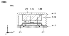
- FIG. 1B is a cross-sectional view showing the non-reciprocal circuit device of Comparative Example 2.
- FIG. 2 is an equivalent circuit of the nonreciprocal circuit device according to the first embodiment.
- FIG. 3 is a perspective view of the non-reciprocal circuit device according to the first embodiment.
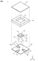
- FIG. 4 is an exploded perspective view of the non-reciprocal circuit device according to the first embodiment.
- FIG. 5A is a diagram showing a cut surface when the non-reciprocal circuit device shown in FIG. 3 is cut along a VA-VA line.
- FIG. 5B is a diagram showing magnetic flux in the non-reciprocal circuit device of FIG. 5A.
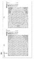
- FIG. 6A and 6B are diagrams showing the magnetic flux density distribution of ferrite.
- FIG. 6A shows a case where the distance between the first yoke and the ferrite is 0.05 mm
- FIG. It is a figure which shows the case of 02 mm.
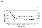
- FIG. 7 is a diagram showing non-uniformity of the magnetic flux density of ferrite and insertion loss of the nonreciprocal circuit element.
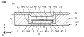
- FIG. 8 is a diagram illustrating a cut surface of the non-reciprocal circuit device according to the modification of the first embodiment.
- FIG. 9 is a functional block diagram illustrating the communication apparatus according to the second embodiment.
- FIG. 10 is an exploded perspective view of ferrite in another embodiment.
- FIG. 1A is a cross-sectional view showing a non-reciprocal circuit device 501 of Comparative Example 1.
- FIG. 1A is a cross-sectional view showing a non-reciprocal circuit device 501 of Comparative Example 1.
- the non-reciprocal circuit element 501 of Comparative Example 1 includes a ferrite 540 including a ferrite element 541 and a central conductor 542, a pair of magnets 530 located outside the side surface of the ferrite 540, and a ferrite 540 and a pair of magnets 530 below.
- a first yoke 510 provided and a second yoke 520 provided above the ferrite 540 and the pair of magnets 530 are provided.
- the magnet 530 has an N pole on the upper side and an S pole on the lower side.
- Ferrite 540 is electrically connected to first yoke 510 using solder 551. In the non-reciprocal circuit element 501, the ferrite 540 is in contact with the first yoke 510.
- the magnetic flux B in the non-reciprocal circuit element 501 is generated so as to pass through the magnet 530, the second yoke 520, the ferrite 540, and the first yoke 510 and return to the magnet 530.
- the direction of the magnetic flux B passing through the outer peripheral portion (both ends in the X direction) of the ferrite 540 changes so that the magnetic resistance is reduced in the vicinity of the boundary between the ferrite 540 and the first yoke 510.
- the direction of the magnetic flux B changes from the thickness direction (Z direction) of the ferrite 540 to the direction along the main surface of the first yoke 510 (X direction) before the first yoke 510.
- the magnetic flux density in the Z direction of the ferrite 540 is smaller in the outer peripheral portion than in the central portion, and the magnetic flux density distribution in the XY plane of the ferrite 540 becomes nonuniform. As a result, there is a problem that the insertion loss increases in the non-reciprocal circuit device 501 of Comparative Example 1.
- the magnetic flux density distribution in the vicinity of the second yoke 520 is improved, but in the vicinity of the boundary between the ferrite 540 and the first yoke 510.
- the magnetic flux density distribution cannot be made uniform, and the same problem as described above may occur.
- FIG. 1B is a cutaway view showing the non-reciprocal circuit element 601 of Comparative Example 2.
- the magnet 630 is disposed above the ferrite 640.
- the non-reciprocal circuit element 601 of Comparative Example 2 includes a ferrite 640 including a ferrite element 641 and a central conductor 642, a support substrate 610 that supports the ferrite 640, a magnet 630 disposed on the upper side of the ferrite 640, and a magnet 630. And a cylindrical case 620 provided so as to support the surface and cover the ferrite 640.
- the magnet 630 has an N pole on the lower side and an S pole on the upper side.
- Ferrite 640 is electrically connected to support substrate 610 using solder 651.
- the magnetic flux B generated in the non-reciprocal circuit element 601 is generated from the magnet 630 so as to pass through the ferrite 640.
- the magnetic flux B passing through the outer peripheral portion (both ends in the X direction) of the ferrite 640 is generated along the magnetic field lines of the magnet 630. Therefore, the magnetic flux density in the Z direction of the ferrite 640 is smaller in the outer peripheral portion than in the central portion, and the magnetic flux density distribution in the XY plane of the ferrite 640 becomes nonuniform.
- the inventor arranges the magnet 530 outside the side surface of the ferrite 540 so that the magnetic flux density of the outer peripheral portion of the ferrite 540 does not become small, and the position where the direction of the magnetic flux B changes.
- the idea is that the ferrite 540 may be disposed away from the first yoke 510 so that the ferrite 540 does not exist in the first yoke 510.
- each figure is a schematic diagram and is not necessarily shown strictly. Moreover, in each figure, the same code
- the Z direction in each figure means the thickness direction of the ferrite or the direction in which the first yoke and the second yoke face each other.
- Non-reciprocal circuit elements shown in the following embodiments are surface-mount elements, and are mounted on, for example, mobile phone base stations.
- the nonreciprocal circuit element passes a transmission signal from the transmission side circuit to the antenna and passes a reception signal received by the antenna to the reception circuit. That is, the non-reciprocal circuit element has a characteristic that allows a signal to pass only in a predetermined specific direction and does not substantially pass the reverse direction.
- FIG. 2 is an equivalent circuit of the non-reciprocal circuit device 1 according to the first embodiment.
- FIG. 3 is a perspective view of the non-reciprocal circuit device 1.
- the nonreciprocal circuit device 1 is a lumped constant type three-port circulator having the equivalent circuit shown in FIG. That is, the first center conductor 121 (L1), the second center conductor 122 (L2), and the third center conductor 123 (L3) are attached to the rectangular microwave ferrite element 41 to which the DC magnetic field B is applied by the permanent magnet 30.
- Each of the first central conductors 121 is arranged in an insulated state so as to intersect at a predetermined angle.
- One end of the first central conductor 121 is the first port P101.
- One end of the second central conductor 122 is the second port P102.
- Port P103 is set.
- each of the central conductors 121, 122, 123 is connected to GND (ground).
- Capacitance elements C1, C2, and C3 are connected in parallel to the central conductors 121, 122, and 123, respectively.
- a capacitive element Cs1 is connected between the first port P101 and the transmission terminal TX
- a capacitive element Cs2 is connected between the second port P102 and the reception terminal RX
- the third port P103 and the antenna terminal are connected.
- a capacitive element Cs3 is connected to the ANT.
- the capacitive elements C1, C2, and C3 are for adjusting the resonance frequency
- the capacitive elements Cs1, Cs2, and Cs3 are for matching impedances.
- the non-reciprocal circuit device 1 having the above equivalent circuit includes, as shown in FIG. 3, a ferrite 40 (magnetic) having a ferrite element 41 and a central conductor 42 (corresponding to the central conductors 121, 122, and 123).
- the rotor ), the substantially permanent magnet 30 surrounding the side surface of the ferrite 40, the first yoke 10 disposed on the mounting surface side of the ferrite 40, and the second yoke 20 disposed on the top surface side. It is configured.
- the capacitive elements C1, C2, C3, Cs1, Cs2, and Cs3 are chip components, and may be disposed on a substrate (PCB or LTCC) on which the nonreciprocal circuit device 1 of FIG. It may be formed inside.
- one end (port P101) of the first center conductor 121 is used as the external connection electrode 141, the other end is used as the external connection electrode 142, and one end (port P102) of the second center conductor 122 is used.
- the nonreciprocal circuit device 1 When the nonreciprocal circuit device 1 is incorporated in a transmission / reception circuit unit (front end circuit) such as a mobile phone, the first port P101 (electrode 141) is connected to the transmission side (TX) and the second port P102 (electrode 143) is connected to the receiving side (RX), and the third port P103 (electrode 145) is connected to the antenna side (ANT).
- TX transmission side
- RX receiving side
- ANT antenna side
- the operation of the nonreciprocal circuit element 1 (3-port circulator) in the front-end circuit is as follows. That is, the high frequency signal input from the first port P101 (transmission circuit) is output from the third port P103 (ANT), and the high frequency signal input from the third port P103 (ANT) is the second port P102 (reception circuit). ). The high frequency signal of the second port P102 is not attenuated by the front end circuit and transmitted to the first port P101.
- FIG. 4 is an exploded perspective view of the nonreciprocal circuit device 1.
- FIG. 5A is a diagram showing a cut surface when the non-reciprocal circuit device 1 shown in FIG. 3 is cut along a VA-VA line. In FIG. 5A, only the cut surface is shown as a cross section, and the description of the components located on the back side of the paper surface (X direction minus side) is omitted.
- the non-reciprocal circuit element 1 includes a first yoke 10, a second yoke 20 facing the first yoke 10, a permanent magnet 30 and a ferrite 40 disposed between the first yoke 10 and the second yoke 20, A connection conductor 50 provided between the first yoke 10 and the ferrite 40 is provided.
- the first yoke 10 is a flat terminal yoke, and includes three input / output terminals 11 and a ground terminal 12 that is disposed close to the input / output terminals 11 with a space therebetween.
- the input / output terminal 11 is a part for inputting and outputting a high-frequency signal
- the ground terminal 12 is a part grounded to a reference potential.
- An insulating part 13 is provided between the input / output terminal 11 and the ground terminal 12.
- iron (Fe) is used as a material of the input / output terminal 11 and the ground terminal 12.
- silver plating may be applied to the exposed surfaces of the input / output terminal 11 and the ground terminal 12.
- an epoxy resin is used as a material of the insulating part 13, for example.
- the second yoke 20 has a flat flat plate portion 21 and a convex portion 22 that protrudes toward the first yoke 10 at the center of the flat plate portion 21.
- the second yoke 20 may have only the flat plate portion 21 without having the convex portion 22.
- the second yoke 20, together with the first yoke 10, applies a magnetic shunt action to the magnetic field formed by the permanent magnet 30.
- iron is used as the material of the second yoke 20.
- silver plating may be applied to the surface of the second yoke 20.
- the permanent magnet 30 has an annular shape, and one end face that is the outer edge of one magnetic pole (N pole) is joined to the second yoke 20 via an adhesive, and the other end face that is the outer edge of the other magnetic pole (S pole) is It is joined to the first yoke 10 via an adhesive.
- the N pole and the S pole may be reversed.
- the thickness of the permanent magnet 30 is 0.65 mm
- the distance i2 between the first yoke 10 and the second yoke 20 is about 0.65 mm.
- the interval i2 is a distance between the flat plate portion 21 of the second yoke 20 and the first yoke 10.
- the permanent magnet 30 has an opening 35 that penetrates the permanent magnet 30 in the thickness direction.
- a ferrite 40 is accommodated in the opening 35.
- the surface of the ferrite 40 on which the central conductor 42 is formed is the one main surface 40a
- the surface opposite to the one main surface 40a is the other main surface 40b
- the one main surface 40a and the other main surface 40b are combined.
- the permanent magnet 30 is disposed around the side surface 40 c of the ferrite 40. That is, the permanent magnet 30 is disposed outside the side surface 40c of the ferrite 40 as shown in FIG. 5A.
- Ferrite 40 is applied with a DC magnetic field from permanent magnet 30.
- the ferrite 40 has a flat ferrite element 41, three central conductors 42 provided on the ferrite element 41, and six through vias 43.
- the thickness of the ferrite element 41 is 0.15 mm, for example, and is thinner than the permanent magnet 30.
- the ferrite element 41 is a member having magnetism.
- the ferrite element 41 may be formed of a material mainly composed of zinc, nickel, copper, manganese, cobalt, magnesium, lithium, for example.
- the ferrite element 41 may be formed of a material containing iron oxide as a main component and containing at least one of zinc, nickel, and copper.
- the central conductor 42 is provided on the upper surface (the surface facing the second yoke 20) of the ferrite element 41.
- An insulator layer (not shown) is provided between the central conductors 42, and the central conductors 42 are arranged so as to intersect each other at a predetermined angle.
- Each of the center conductors 42 is a so-called internal conductor (also referred to as a center electrode) of the nonreciprocal circuit element 1 and can be formed on the ferrite element 41 as a thin film conductor, a thick film conductor, or a conductor foil.
- the through via 43 is provided on the side surface 40c of the ferrite 40 so as to penetrate the ferrite element 41 in the thickness direction.
- the six through vias 43 are connected to one end and the other end of each of the three central conductors 42 in a one-to-one correspondence.
- a material of the central conductor 42 and the through via 43 for example, a metal or alloy mainly containing silver is used.
- connection conductors 50 are provided on the other main surface 40 b of the ferrite 40.
- the connection conductor 50 is a member that electrically connects the first yoke 10 and the ferrite 40, and is also a spacer that supports the ferrite 40 at a position away from the first yoke 10.
- the connection conductor 50 By disposing the connection conductor 50 between the first yoke 10 and the ferrite 40, the ferrite 40 is provided at a position away from the first yoke 10 by a predetermined distance i1.
- the predetermined distance i1 is a distance between the one main surface 10a of the first yoke 10 and the other main surface 40 of the ferrite 40, and is 0.05 mm or more and 0.325 mm or less in the present embodiment.
- the upper limit of the predetermined distance i1 is preferably set to be equal to or less than 1 ⁇ 2 of the interval i2 between the first yoke 10 and the second yoke 20 so that the ferrite 40 does not approach the second yoke 20 too much. .
- connection conductors 50 has a short column shape, and the length in the axial direction (Z direction) is, for example, 0.04 mm or more and 0.315 mm or less.
- the connection conductor 50 protrudes from the other main surface 40b of the ferrite 40 toward the first yoke 10 side.
- One end surfaces of the six connection conductors 50 are in contact with and connected to the six through vias 43 in a one-to-one correspondence.
- the other end surfaces of the six connection conductors 50 are connected to the corresponding three ground terminals 12 and the three input / output terminals 11 via solder 51, respectively.
- connection conductor 50 is, for example, a terminal electrode formed on the ferrite 40, and is made of at least one metal of Pt, Ag, Cu, Au, Ni, Pd, Sn, or an alloy of at least two of the metals. Including.
- the connection conductor 50 may be formed by a printing method, a thin film formation method, or a photolithography method, or may be formed by joining a metal plate (metal foil) to the other main surface 40 b of the ferrite 40.
- FIG. 5B is a diagram showing the magnetic flux B in the nonreciprocal circuit device 1.
- the magnetic flux B is generated so as to pass through the permanent magnet 30, the second yoke 20, the ferrite 40 and the first yoke 10 and return to the permanent magnet 30.
- the direction of the magnetic flux B passing through the outer periphery of the ferrite 40 changes so that the magnetic resistance is reduced in the vicinity of the boundary between the ferrite 40 and the first yoke 10.
- the direction of the magnetic flux B changes from the thickness direction (Z direction) of the ferrite 40 to the direction (X direction) along the one main surface 10a of the first yoke 10 before the first yoke 10.
- a connection conductor 50 is provided between the first yoke 10 and the ferrite 40.
- the ferrite 40 is separated from the first yoke 10 by a predetermined distance i1. Therefore, the ferrite 40 can be located in the first region A1 in which the directions of the magnetic flux are aligned, and the difference in the magnetic flux density in the Z direction between the outer peripheral portion and the central portion of the ferrite 40 can be reduced. As a result, the insertion loss of the nonreciprocal circuit element 1 can be reduced.
- the nonreciprocal circuit element 1 is less likely to change in magnetic flux density when the ferrite 40 is present in the first region A1.
- the magnitude of the magnetic flux density changes as the distance between the magnet 530 and the ferrite 540 changes, but the non-reciprocal circuit element 1 of the present embodiment.
- the other yoke for example, the second yoke 20
- the nonreciprocal circuit element 1 can suppress variations in electrical characteristics caused by variations in the height position of the ferrite 40 as compared with the comparative example 2.
- the magnetic flux density below refers to the magnetic flux density in the thickness direction of the ferrite 40.
- FIG. 6 is a diagram showing the magnetic flux density distribution of the ferrite 40 by magnetic field analysis.
- FIG. 6A shows a case where the distance i1 between the first yoke 10 and the ferrite 40 is 0.05 mm
- FIG. It is a figure which shows the case where distance i1 with a ferrite 40 is 0.02 mm.
- Each of (a) and (b) is a magnetic flux density distribution of a cross section (XY plane) at the center in the thickness direction of the ferrite 40.
- the dimensions of the ferrite 40 were 2 mm in length, 2 mm in width, and 0.15 mm in thickness.
- the dimensions of the permanent magnet 30 were such that the outer shape was 4 mm long, 4 mm wide, and 0.65 mm thick, and the opening 35 was 2.5 mm long and 2.5 mm wide.
- the strength of the permanent magnet 30 was 500 mT.
- the thickness of the first yoke 10 was 0.15 mm, and the thickness of the flat plate portion 21 of the second yoke 20 was 0.15 mm.
- the difference in magnetic flux density between the central portion and the outer peripheral portion of the ferrite 40 is large, and the difference between the maximum value and the minimum value is 159 mT.
- the difference in magnetic flux density between the central portion and the outer peripheral portion of the ferrite 40 is small, and the difference between the maximum value and the minimum value is 59 mT.
- the difference in magnetic flux density between the central portion and the outer peripheral portion is smaller than when the distance i1 is 0.02 mm.
- FIG. 7 is a diagram showing the non-uniformity of the magnetic flux density of the ferrite 40 and the insertion loss of the nonreciprocal circuit element 1.
- the non-uniformity of the magnetic flux density is a value obtained from the following formula based on the magnetic flux density distribution of the ferrite 40 shown in FIG.
- Magnetic flux density non-uniformity (%) (Maximum magnetic flux density-Minimum value) / Average magnetic flux density
- the non-uniformity of the magnetic flux density when the distance i1 is 0.05 mm is 18%
- the non-uniformity of the magnetic flux density when the distance i1 is 0.02 mm is 47%.
- FIG. 7 is a graph showing the non-uniformity of the magnetic flux density when the distance i1 between the first yoke 10 and the ferrite 40 is changed at a pitch of 0.01 mm.
- the thin curve in FIG. 7 is a graph showing the insertion loss of the nonreciprocal circuit device 1 when the distance i1 is similarly changed.
- the distance i1 when the distance i1 is less than 0.05 mm, the non-uniformity of the magnetic flux density is large and the insertion loss is also large.
- the distance i1 is 0.05 mm or more and 0.12 mm or less, the non-uniformity of the magnetic flux density is small and the insertion loss is reduced.
- the nonreciprocal circuit device 1 shown in the present embodiment includes the first yoke 10, the second yoke 20 facing the first yoke 10, the ferrite element 41, and the central conductor 42.
- the permanent magnet 30 provided between the ferrite 40 disposed between the two yokes 20, the first yoke 10 and the second yoke 20 and outside the side surface 40 c of the ferrite 40, and the first yoke 10.
- a connecting conductor 50 that electrically connects the ferrite 40 to each other.
- the connection conductor 50 is provided between the first yoke 10 and the ferrite 40.
- the ferrite 40 can be separated from the first yoke 10, and the position where the direction of the magnetic flux is aligned as much as possible (with the first yoke 10 and The ferrite 40 can be provided in a direction in which the second yoke 20 faces the position where the direction of the magnetic flux does not change.
- the difference of the magnetic flux density in the outer peripheral part and the center part of the ferrite 40 can be made small, and the insertion loss of the nonreciprocal circuit element 1 can be reduced.
- FIG. 8 is a diagram illustrating a cut surface of the non-reciprocal circuit device 1A according to the modification of the first embodiment.
- connection conductor 50A is formed of a solder material.
- the non-reciprocal circuit device 1A includes a first yoke 10, a second yoke 20 facing the first yoke 10, a permanent magnet 30 and a ferrite 40 disposed between the first yoke 10 and the second yoke 20, A connection conductor 50A provided between the first yoke 10 and the ferrite 40 is provided.
- An insulating layer made of a solder resist 52 is provided in a region between the first yoke 10 and the ferrite 40 and different from the region where the connection conductor 50A is provided.
- the ferrite 40 is supported by the solder resist 52.
- the ferrite 40 has a flat ferrite element 41, three central conductors 42 provided in the ferrite element 41, six through vias 43, and six terminal electrodes 45.
- the six through vias 43 are provided on the side surface 40c of the ferrite 40, and are connected to one end and the other end of each of the three central conductors 42 in a one-to-one correspondence.
- the six terminal electrodes 45 are connected to each of the six through vias 43 in a one-to-one correspondence.
- the terminal electrode 45 is formed to be embedded inside the other main surface 40 b of the ferrite 40.
- the modified connection conductor 50A is formed of solder that electrically connects the first yoke 10 and the ferrite 40.
- the connection conductor 50 ⁇ / b> A and the solder resist 52 between the first yoke 10 and the ferrite 40 the ferrite 40 is provided at a position away from the first yoke 10.
- One of the six connection conductors 50A is connected to the six terminal electrodes 45 in a one-to-one correspondence, and the other of the six connection conductors 50A is connected to the corresponding three ground terminals 12 and three input / output terminals 11, respectively. Is done.
- the non-reciprocal circuit device 1A of the present modified example provides the connecting conductor 50A and the solder resist 52 between the first yoke 10 and the ferrite 40, thereby separating the ferrite 40 from the first yoke 10 so that the direction of the magnetic flux is as much as possible.
- the ferrite 40 is provided at the position where the Thereby, the difference of the magnetic flux density in the outer peripheral part and center part of the ferrite 40 can be made small, and the insertion loss of 1 A of nonreciprocal circuit elements can be reduced.
- the present invention can be realized not only as the above-described non-reciprocal circuit element, but also as a front-end circuit and a communication device including such a non-reciprocal circuit element. Therefore, hereinafter, a communication apparatus including the above-described non-reciprocal circuit element (that is, a communication apparatus incorporating a front-end circuit including the non-reciprocal circuit element) will be described.
- FIG. 9 is a functional block diagram of the communication device 3 including the nonreciprocal circuit element 1 described in the first embodiment.
- the communication device 3 is a base station of a mobile phone, for example, including a front-end circuit 2 having a nonreciprocal circuit element 1, an RFIC (Radio Frequency Integrated Circuit) 200, and an antenna element 300. . Note that the communication device 3 may not include the antenna element 300.
- the front end circuit 2 is provided at the front end of the communication device 3 and propagates a transmission signal or a reception signal between the RFIC 200 and the antenna element 300.
- the front end circuit 2 further includes a transmission side circuit such as a PA (Power Amplifier) 202, variable filters 206a and 206b, and a BPF (Band Pass Filter). ) 203a and 203b and a receiving circuit such as LNA (Low Noise Amplifier) 204.
- the front end circuit 2 is provided with a transmission terminal Ptx to which a transmission signal is input, an antenna terminal Pant to which the transmission signal is output and a reception signal is input, and a reception terminal Prx that outputs the reception signal.
- the front end circuit 2 may not include the variable filters 206a and 206b, and may include a matching circuit other than the above or a transmission or reception filter.
- the non-reciprocal circuit device 1 has a first port Port1, a second port Port2, and a third port Port3 corresponding to the three input / output terminals 11.
- the first port Port1 is connected to the transmission side circuit (PA202 here) via the variable filter 206a and the BPF 203a
- the second port Port2 is connected to the reception circuit (here LNA204) via the variable filter 206b and the BPF 203b.
- the third port Port 3 is connected to the antenna terminal Pant via the tuner 205.
- the first port Port1 is connected to the transmission terminal Ptx via the PA 202
- the second port Port2 is connected to the reception terminal Prx via the LNA 204.
- PA 202 is, for example, a power amplification module that amplifies a transmission signal (high-frequency transmission signal) input from the transmission terminal (TX in the drawing) of the RFIC 200 to the transmission terminal Ptx of the front end circuit 2.
- the BPF 203a passes the transmission signal output from the nonreciprocal circuit element 1 after filtering it in a predetermined use frequency band. Further, the BPF 203b passes the received signal input from the antenna terminal Pant after filtering in the use frequency band.
- the LNA 204 is, for example, a low noise amplification module that amplifies the reception signal (high frequency reception signal) output from the nonreciprocal circuit element 1.
- Such a front-end circuit 2 amplifies and filters the transmission signal input to the transmission terminal Ptx and outputs it from the antenna terminal Pant, and filters and amplifies the reception signal input to the antenna terminal Pant from the reception terminal Prx. Output.
- the transmission signal passes through the Tx path of the nonreciprocal circuit element 1, and the reception signal passes through the Rx path of the nonreciprocal circuit element 1.
- the RFIC 200 is a circuit that is connected to the transmission terminal Ptx and the reception terminal Prx of the front-end circuit 2 and processes the transmission signal or the reception signal. For example, the RFIC 200 up-converts a transmission signal input from a baseband signal processing circuit (not shown) and outputs it from a transmission terminal (TX in the figure), and inputs from the front end circuit 2 to a reception terminal (RX in the figure). The received signal is down-converted and output to the baseband signal processing circuit (BBIC) 201.
- BBIC baseband signal processing circuit
- the antenna element 300 is connected to the antenna terminal Pant of the front end circuit 2, and transmits a transmission signal and receives a reception signal.
- the shape or the like of the antenna element 300 is not particularly limited, and may be appropriately designed according to the use frequency band of the communication device 3.
- the communication quality can be improved by providing the nonreciprocal circuit element 1 with reduced insertion loss.
- the pair of side surfaces 31 facing each other is configured by using the annular permanent magnets 30.
- the present invention is not limited to this, and the two permanent magnets facing each other are arranged to face each other.
- a pair of side surfaces may be configured.
- a gap is formed in a region between the first yoke 10 and the ferrite 40 and different from the region in which the connection conductor 50 is provided.
- a resist may be provided.
- a spacer may be provided between the first yoke 10 and the permanent magnet 30 or between the permanent magnet 30 and the second yoke 20.
- the central conductor 42 provided in the ferrite 40 may be a lumped constant type or a distributed constant type.
- the nonreciprocal circuit device may be a two-port isolator having an input port and an output port.
- the ferrite 40 of the nonreciprocal circuit device may have the structure shown in FIG. Specifically, the ferrite 40 is formed by laminating insulator layers 111, 112, 113, 114 mainly composed of glass, various conductors, and various electrodes on the top surface side and the mounting surface side of the rectangular microwave ferrite 40.
- the ferrite 40 is also provided with a plurality of through-hole conductors and a plurality of electrodes for connecting various conductors provided on the top surface side and the mounting surface side in a coil shape.
- the conductors 121a, 121b, and 121c forming the first central conductor 121 (L1) are formed on the insulator layer 112, and the conductors 121d and 121e are formed between the insulator layer 113 and the ferrite element 41.
- An end portion of the conductor 121a is an external lead portion 141a
- an end portion of the conductor 121c is an external lead portion 142a.
- the other end of the conductor 121a is connected to one end of the conductor 121d through the conductor 121f
- the other end of the conductor 121d is connected to one end of the conductor 121b through the conductor 121g.
- the other end of the conductor 121b is connected to one end of a conductor 121e through a conductor 121h, and the other end of the conductor 121e is connected to one end of a conductor 121c through a conductor 121i.
- the conductors 122a, 122b, and 122c forming the second central conductor 122 (L2) are formed between the insulator layer 111 and the ferrite element 41, and the conductors 122d and 122e are formed on the lower surface of the insulator layer 114.
- An end portion of the conductor 122a is an external lead portion 143a
- an end portion of the conductor 122c is an external lead portion 144a.
- the other end of the conductor 122a is connected to one end of the conductor 122d through the conductor 122f, and the other end of the conductor 122d is connected to one end of the conductor 122b through the conductor 122g.
- the other end of the conductor 122b is connected to one end of the conductor 122e through the conductor 122h
- the other end of the conductor 122e is connected to one end of the conductor 122c through the conductor 122i.
- the conductors 123a, 123b and 123c forming the third central conductor 123 (L3) are formed between the insulator layers 111 and 112, and the conductors 123d and 123e are formed between the insulator layers 113 and 114.
- the end portion of the conductor 123a is an external lead portion 146a, and the end portion of the conductor 123c is an external lead portion 145a.
- the other end of the conductor 123a is connected to one end of the conductor 123d through the conductor 123f, and the other end of the conductor 123d is connected to one end of the conductor 123b through the conductor 123g.
- the other end of the conductor 123b is connected to one end of a conductor 123e through a conductor 123h, and the other end of the conductor 123e is connected to one end of a conductor 123c through a conductor 123i.
- the external connection electrode 141 is formed by an external lead portion 141a that is an end portion of the conductor 121a and an electrode connected to the external lead portion 141a.
- the external connection electrode 142 is formed by an external lead portion 142a that is an end portion of the conductor 121c and an electrode connected thereto.
- the external connection electrode 143 is formed by an external lead portion 143a which is an end portion of the conductor 122a and an electrode connected thereto.
- the external connection electrode 144 is formed by an external lead portion 144a that is an end portion of the conductor 122c and an electrode connected to the external lead portion 144a.
- the external connection electrode 145 is formed by an external lead portion 145a that is an end portion of the conductor 123c and an electrode connected to the external lead portion 145a.
- the external connection electrode 146 is formed by an external lead portion 146a that is an end portion of the conductor 123a and an electrode connected thereto.
- the central conductors 121, 122, and 123 can be formed as a thin film conductor such as Ag or Cu, a thick film conductor, or a conductive foil, and it is preferable to use a photosensitive metal paste.
- the insulator layers 111 to 114 are preferably made of a material having high insulation resistance such as photosensitive glass or polyimide.
- the conductor layer and the insulating layer can be formed by photolithography, etching, printing, or the like.
- the external connection electrodes 141 to 146 and the through-hole conductor are preferably coated with a conductive electrode material (paste) mainly composed of Ag and Cu and baked to form a Ni plating layer on the surface, Further, a plating layer of Au, Sn, Ag, Cu or the like is formed. It is not limited to plating, but may be a sputtering process or the like.
- the capacitor elements C1, C2, C3, etc. use chip parts.
- the ferrite 40 is disposed in a substantially frame-shaped permanent magnet 30, the first yoke 10 is disposed on the mounting surface side, and the second yoke 20 is disposed on the top surface side, thereby forming a nonreciprocal circuit element. Is done.
- the present invention can be widely used in communication devices such as mobile phone base stations as non-reciprocal circuit elements arranged in the front end of the communication device.
Landscapes
- Non-Reversible Transmitting Devices (AREA)
Abstract
非可逆回路素子(1)は、第1ヨーク(10)と、第1ヨーク(10)に対向する第2ヨーク(20)と、フェライト素子(41)および中心導体(42)を含み、第1ヨーク(10)と第2ヨーク(20)との間に配置されたフェライト(40)と、第1ヨーク(10)と第2ヨーク(20)との間であって、フェライト(40)の側面(40c)の外側に設けられた永久磁石(30)と、第1ヨーク(10)とフェライト(40)とを電気的に接続する接続導体(50)とを備えている。接続導体(50)は、第1ヨーク(10)とフェライト(40)との間に設けられている。
Description
本発明は、非可逆回路素子、この非可逆回路素子を備えるフロントエンド回路および通信装置に関する。
アイソレータやサーキュレータ等の非可逆回路素子は、予め定められた特定方向にのみ信号を通過させ、逆方向には実質的に通過させない特性を有している。このような非可逆回路素子として、フェライトの非可逆性を利用した構成が知られている(例えば、特許文献1参照)。
特許文献1に記載された非可逆回路素子は、フェライト素子および中心導体を含むフェライトと、フェライトの側面の外側に設けられた一対の磁石と、フェライトおよび一対の磁石の下側に設けられた第1ヨークと、フェライトおよび一対の磁石の上側に設けられた第2ヨークとを備えている。この非可逆回路素子では、第2ヨークに複数の貫通孔を設けてフェライトに到達する磁束を均一化させることで、挿入損失を低減している。
例えば、フェライトの上部に磁石を配置し、フェライトの下部にヨークを配置する構造の非可逆回路素子の場合、磁気回路構造が非対称となり磁束の均一性が悪く、非可逆回路素子の挿入損失が劣化する。
また、特許文献1に記載されている非可逆回路素子では、フェライトの上下面がヨークで挟まれており磁気回路構造が対称であるので、基本的にはフェライトを通過する磁束の均一性が優れ、低挿入損失の非可逆回路素子が得られる。しかしながら、フェライトの下部を通過する磁束の向きが揃わず、磁束が均一にならない場合があり、非可逆回路素子の挿入損失を低減しきれないという問題がある。
そこで、本発明は、非可逆回路素子等の挿入損失を低減することを目的とする。
上記目的を達成するために、本発明の一態様に係る非可逆回路素子は、第1ヨークと、第1ヨークに対向する第2ヨークと、フェライト素子および中心導体を含み、第1ヨークと第2ヨークとの間に配置されたフェライトと、第1ヨークと第2ヨークとの間であって、フェライトの側面の外側に設けられた永久磁石と、第1ヨークとフェライトとを電気的に接続する接続導体と、を備え、接続導体は、第1ヨークとフェライトとの間に設けられている。
このように、接続導体を第1ヨークとフェライトとの間に設けることで、フェライトを第1ヨークから離すことができ、できるだけ磁束の向きが揃った位置にフェライトを設けることができる。これにより、フェライト内における磁束密度の差を小さくすることができ、非可逆回路素子の挿入損失を低減することができる。
また、フェライトは、第2ヨークに対向する一方主面と、第1ヨークに対向する他方主面とを有し、接続導体は、フェライトの他方主面に形成された端子電極であり、フェライトの他方主面から前記第1ヨーク側に向かって突出していてもよい。
このように、接続導体をフェライトから第1ヨーク側に向かって突出させることで、フェライトを第1ヨークから離し、できるだけ磁束の向きが揃った位置にフェライトを設けることができる。これにより、フェライト内における磁束密度の差を小さくすることができ、非可逆回路素子の挿入損失を低減することができる。
また、接続導体は、はんだを介して第1ヨークに接続されていてもよい。
これによれば、接続導体と第1ヨークとの電気的および機械的な接続性を向上することができ、非可逆回路素子の電気特性の低下を抑制することができる。
また、フェライトは、第1ヨークから所定距離、離れた位置に設けられており、所定距離は、0.05mm以上であってもよい。
これによれば、フェライトを第1ヨークから所定距離離し、磁束の向きが揃った位置にフェライトを設けることができる。これにより、フェライト内における磁束密度の差を小さくすることができ、非可逆回路素子の挿入損失を低減することができる。
また、所定距離は、第1ヨークと第2ヨークとの間隔の1/2以下であってもよい。
これによれば、フェライトが第2ヨークに近づき過ぎて、磁束の向きが揃った位置から外れることを抑制することができる。これにより、フェライト内における磁束密度の差を小さくすることができ、非可逆回路素子の挿入損失を低減することができる。
また、フェライトは、フェライト素子を厚み方向に貫通して中心導体に接続する貫通ビアを有し、貫通ビアは、接続導体に接続されていてもよい。
これによれば、厚み方向に垂直な方向のフェライトの寸法を小さくすることができ、また、フェライトと永久磁石との距離を縮めることができ、非可逆回路素子を小型化することができる。
また、接続導体は、Pt、Ag、Cu、Au、Ni、Pd、Snのうちの少なくとも1つの金属、または、上記金属のうちの少なくとも2以上の合金を含んでいてもよい。
これによれば、接続導体の電気抵抗を小さくすることができ、非可逆回路素子の電気特性の低下を抑制することができる。
また、第1ヨークとフェライトとの間であって、接続導体が設けられた領域と異なる領域に、ソルダーレジストが設けられていてもよい。
これによれば、フェライトをソルダーレジストで支持することができ、フェライトの位置を安定化することができる。
また、永久磁石は、環状であり、フェライトの周囲に設けられていてもよい。
これによれば、フェライトの外周部と中央部との磁束密度の差を小さくすることができ、非可逆回路素子の挿入損失を低減することができる。
また、フェライトは、3つの中心導体を有し、第1ヨークは、3つの中心導体に接続する3つの入出力端子を有していてもよい。
これによれば、フェライト素子の磁束密度が大きい3ポート型の非可逆回路素子を提供することができる。
また、本発明は上述した非可逆回路素子として実現できるだけでなく、非可逆回路素子を備えるフロントエンド回路としても実現できる。つまり、上記目的を達成するために、本発明の一態様に係るフロントエンド回路は、上記非可逆回路素子と、3つの入出力端子のうちの1つに接続される送信側回路と、3つの入出力端子のうちの1つであって、送信側回路に接続された入出力端子と異なる入出力端子に接続される受信側回路と、3つの入出力端子のうちの1つであって、送信側回路および受信側回路に接続されたそれぞれの入出力端子と異なる入出力端子に接続されるアンテナ端子と、を備える。
このようなフロントエンド回路によれば、フェライト素子の磁束密度が大きい非可逆回路素子を備えることにより、所望の通過特性を実現することが可能となる。
また、さらには、本発明は上述したフロントエンド回路としてだけでなく、フロントエンド回路を備える通信装置としても実現できる。つまり、上記目的を達成するために、本発明の一態様に係る通信装置は、高周波信号を処理する信号処理回路と、上記フロントエンド回路と、を備える。
このような通信装置によれば、挿入損失が低減された非可逆回路素子を備えることにより、通信品質の向上を図ることができる。
本発明は、非可逆回路素子等の挿入損失を低減することができる。
(本発明の基礎となった知見)
本発明者は、「背景技術」の欄に記載した非可逆回路素子に関して、以下の問題が生じることを見出した。以下、「背景技術」に関連する非可逆回路素子の一例として、比較例1の非可逆回路素子を、他の一例として、比較例2の非可逆回路素子を説明する。
本発明者は、「背景技術」の欄に記載した非可逆回路素子に関して、以下の問題が生じることを見出した。以下、「背景技術」に関連する非可逆回路素子の一例として、比較例1の非可逆回路素子を、他の一例として、比較例2の非可逆回路素子を説明する。
図1Aは、比較例1の非可逆回路素子501を示す断面図である。
比較例1の非可逆回路素子501は、フェライト素子541および中心導体542を含むフェライト540と、フェライト540の側面の外側に位置する一対の磁石530と、フェライト540および一対の磁石530の下側に設けられた第1ヨーク510と、フェライト540および一対の磁石530の上側に設けられた第2ヨーク520とを備えている。磁石530は上側がN極であり、下側がS極である。フェライト540は、はんだ551を用いて第1ヨーク510に電気的に接続されている。この非可逆回路素子501では、フェライト540が第1ヨーク510に接する構造となっている。
非可逆回路素子501内の磁束Bは、磁石530、第2ヨーク520、フェライト540および第1ヨーク510を通過して磁石530に戻るように発生する。ここで、フェライト540の外周部(X方向の両端部)を通過する磁束Bは、フェライト540と第1ヨーク510との境界付近において、磁気抵抗が小さくなるようにその向きが変化する。具体的には、磁束Bの向きが、第1ヨーク510の手前にて、フェライト540の厚み方向(Z方向)から第1ヨーク510の主面に沿う方向(X方向)に変化する。そのため、フェライト540のZ方向の磁束密度は、中央部よりも外周部が小さくなり、フェライト540のXY平面における磁束密度分布が不均一となる。これにより、比較例1の非可逆回路素子501にて挿入損失が大きくなるという問題がある。
なお、「背景技術」に示すように第2ヨーク520に貫通孔を設けた場合は、第2ヨーク520付近における磁束密度分布は改善されるが、フェライト540と第1ヨーク510との境界付近における磁束密度分布を均一にすることはできず、上記と同様の問題が起こり得る。
図1Bは、比較例2の非可逆回路素子601を示す切断図である。比較例2の非可逆回路素子601は、磁石630がフェライト640の上側に配置されている。
比較例2の非可逆回路素子601は、フェライト素子641および中心導体642を含むフェライト640と、フェライト640を支持する支持基板610と、フェライト640の上側に配置された磁石630と、磁石630を天面から支持し、フェライト640を覆うように設けられた筒状のケース620とを備えている。磁石630は、下側がN極であり、上側がS極である。フェライト640は、はんだ651を用いて支持基板610に電気的に接続されている。
非可逆回路素子601に発生する磁束Bは、磁石630からフェライト640を通過するように発生する。ここで、フェライト640の外周部(X方向の両端部)を通過する磁束Bは、磁石630の磁力線に沿って発生する。そのため、フェライト640のZ方向の磁束密度は、中央部よりも外周部が小さくなり、フェライト640のXY平面における磁束密度分布が不均一となる。このように、フェライト640の上側に磁石630が配置されている比較例2の非可逆回路素子601では、磁束密度分布が不均一となりやすく、挿入損失が大きくなるという問題がある。
このような問題を解決するため、本発明者は、フェライト540の外周部の磁束密度が小さくならないように、磁石530をフェライト540の側面の外側に配置するとともに、磁束Bの向きが変化する位置にフェライト540が存在しないように、フェライト540を第1ヨーク510から離して配置すればよいという着想に至った。
以下、図面を参照しながら、本発明の実施の形態に係る非可逆回路素子等の構造について説明する。なお、以下で説明する実施の形態は、いずれも本発明の好ましい一具体例を示すものである。以下の実施の形態で示される数値、形状、材料、構成要素、構成要素の配置位置および接続形態などは、一例であり、本発明を限定する主旨ではない。また、以下の実施の形態における構成要素のうち、最上位概念を示す独立請求項に記載されていない構成要素については、任意の構成要素として説明される。
なお、各図は、模式図であり、必ずしも厳密に図示されたものではない。また、各図において、実質的に同一の構成に対しては同一の符号を付しており、重複する説明は省略又は簡略化する場合がある。各図におけるZ方向は、フェライトの厚み方向、または、第1ヨークと第2ヨークとが対向する方向を意味する。
(実施の形態1)
以下の実施の形態で示す非可逆回路素子は、表面実装型の素子であり、例えば、携帯電話の基地局に搭載される。非可逆回路素子は、送信側回路からの送信信号をアンテナへと通過させ、アンテナで受信された受信信号を受信回路へと通過させる。つまり、非可逆回路素子は、予め定められた特定方向にのみ信号を通過させ、逆方向には実質的に通過させない特性を有している。
以下の実施の形態で示す非可逆回路素子は、表面実装型の素子であり、例えば、携帯電話の基地局に搭載される。非可逆回路素子は、送信側回路からの送信信号をアンテナへと通過させ、アンテナで受信された受信信号を受信回路へと通過させる。つまり、非可逆回路素子は、予め定められた特定方向にのみ信号を通過させ、逆方向には実質的に通過させない特性を有している。
[1-1.非可逆回路素子の基本構成]
まず、図2および図3を参照して、非可逆回路素子1の基本構成を説明する。
まず、図2および図3を参照して、非可逆回路素子1の基本構成を説明する。
図2は、実施の形態1に係る非可逆回路素子1の等価回路である。図3は、非可逆回路素子1の斜視図である。
非可逆回路素子1は、図2に示す等価回路を有する集中定数型の3ポート型サーキュレータである。即ち、永久磁石30により直流磁界Bが印加される、矩形状のマイクロ波フェライト素子41に第1中心導体121(L1)、第2中心導体122(L2)及び第3中心導体123(L3)をそれぞれ絶縁状態で所定の角度で交差させて配置し、第1中心導体121の一端を第1ポートP101、第2中心導体122の一端を第2ポートP102、第3中心導体123の一端を第3ポートP103としている。
さらに、各中心導体121、122、123のそれぞれの他端はGND(グランド)に接続されている。各中心導体121、122、123に対して並列に容量素子C1、C2、C3がそれぞれ接続されている。第1ポートP101と送信用端子TXとの間には容量素子Cs1が接続され、第2ポートP102と受信用端子RXとの間には容量素子Cs2が接続され、第3ポートP103とアンテナ用端子ANTとの間には容量素子Cs3が接続されている。容量素子C1、C2、C3は共振周波数を調整するためのものであり、容量素子Cs1、Cs2、Cs3はインピーダンスを整合させるためのものである。
以上の等価回路からなる非可逆回路素子1は、具体的には、図3に示すように、フェライト素子41および中心導体42(各中心導体121、122および123に相当)を有するフェライト40(磁気回転子)と、フェライト40の側面を囲う略枠形状の永久磁石30と、フェライト40の実装面側に配置された第1ヨーク10と、天面側に配置された第2ヨーク20と、で構成されている。容量素子C1、C2、C3、Cs1、Cs2、Cs3は、チップ部品であり、図3の非可逆回路素子1が実装される基板(PCBやLTCC)上に配置されていてもよいし、当該基板内に形成されていてもよい。
ここで、図2に示すように、第1中心導体121の一端(ポートP101)を外部接続用電極141、他端を外部接続用電極142とし、第2中心導体122の一端(ポートP102)を外部接続用電極143、他端を外部接続用電極144とし、第3中心導体123の一端(ポートP103)を外部接続用電極145、他端を外部接続用電極146とする。また、この非可逆回路素子1が携帯電話などの送受信回路部(フロントエンド回路)に組み込まれる場合、第1ポートP101(電極141)は送信側(TX)に接続され、第2ポートP102(電極143)は受信側(RX)に接続され、第3ポートP103(電極145)はアンテナ側(ANT)に接続される。
フロントエンド回路における非可逆回路素子1(3ポート型サーキュレータ)の動作は以下のとおりである。即ち、第1ポートP101(送信回路)から入力された高周波信号は、第3ポートP103(ANT)から出力され、第3ポートP103(ANT)から入力された高周波信号は第2ポートP102(受信回路)に入力される。第2ポートP102の高周波信号はフロントエンド回路で減衰されて第1ポートP101に伝達されることはない。
[1-2.非可逆回路素子の構成]
次に、図4および図5Aを参照して、非可逆回路素子1の構成を説明する。
次に、図4および図5Aを参照して、非可逆回路素子1の構成を説明する。
図4は、非可逆回路素子1の分解斜視図である。図5Aは、図3に示す非可逆回路素子1をVA-VA線で切断した場合の切断面を示す図である。なお、図5Aでは、切断面のみを断面として示し、紙面奥側(X方向マイナス側)に位置する構成要素の記載を省略している。
非可逆回路素子1は、第1ヨーク10と、第1ヨーク10に対向する第2ヨーク20と、第1ヨーク10と第2ヨーク20との間に配置された永久磁石30およびフェライト40と、第1ヨーク10とフェライト40との間に設けられた接続導体50とを備えている。
第1ヨーク10は、平板状の端子ヨークであり、3つの入出力端子11と、入出力端子11のそれぞれから間隔をあけて近接配置されているグランド端子12とを有している。入出力端子11は高周波信号が入出力される部分であり、グランド端子12は基準電位に接地される部分である。入出力端子11とグランド端子12との間には、絶縁部13が設けられている。入出力端子11およびグランド端子12の材料としては、例えば、鉄(Fe)が用いられる。電気特性を向上させるため、入出力端子11およびグランド端子12の露出面に例えば銀めっきが施されていてもよい。絶縁部13の材料としては、例えば、エポキシ系の樹脂が用いられる。
第2ヨーク20は、平坦な平板部21と、平板部21の中央において第1ヨーク10側に突出する凸部22とを有している。ただし、第2ヨーク20は、凸部22を有せずに、平板部21のみであってもよい。第2ヨーク20は、第1ヨーク10とともに、永久磁石30によって形成される磁界に整磁作用を施す。第2ヨーク20の材料としては、例えば、鉄が用いられる。第2ヨーク20の表面に例えば銀めっきが施されていてもよい。
永久磁石30は、環状であり、一方の磁極(N極)の外縁である一方端面が接着剤を介して第2ヨーク20に接合され、他方の磁極(S極)の外縁である他方端面が接着剤を介して第1ヨーク10に接合されている。なお、N極とS極とは逆であってもよい。例えば、永久磁石30の厚みは0.65mmであり、第1ヨーク10と第2ヨーク20との間隔i2は約0.65mmである。なお、間隔i2は、第2ヨーク20の平板部21と第1ヨーク10との間の距離である。
永久磁石30は、永久磁石30を厚み方向に貫く開口部35を有している。開口部35には、フェライト40が収容されている。ここで、フェライト40において中心導体42が形成されている面を一方主面40aとし、一方主面40aと反対の面を他方主面40bとし、これら一方主面40aおよび他方主面40bをあわせて上下主面(磁場形成時にフェライト40に磁束が入る面)とした場合、永久磁石30はフェライト40の側面40cの周囲に配置されていることになる。すなわち、永久磁石30は、図5Aに示すように、フェライト40の側面40cの外側に配置されている。
フェライト40は、永久磁石30から直流磁界を印加される。フェライト40は、平板状のフェライト素子41と、フェライト素子41に設けられた3つの中心導体42と、6つの貫通ビア43と有している。
フェライト素子41の厚みは、例えば、0.15mmであり、永久磁石30よりも厚さが薄い。フェライト素子41は、磁性を有する部材である。フェライト素子41は、例えば、亜鉛、ニッケル、銅、マンガン、コバルト、マグネシウム、リチウムを主成分とした材料により形成されてもよい。また、フェライト素子41は、酸化鉄を主成分とした、亜鉛、ニッケルおよび銅のうち少なくとも1つ以上を含む材料により形成されてもよい。
中心導体42は、フェライト素子41の上面(第2ヨーク20に対向する面)側に設けられている。中心導体42のそれぞれの間には絶縁体層(不図示)が設けられ、中心導体42は、それぞれが所定の角度で交差するように配置されている。中心導体42のそれぞれは、非可逆回路素子1のいわゆる内部導体(中心電極とも称される)であり、フェライト素子41上に薄膜導体、厚膜導体、または、導体箔として形成することができる。
貫通ビア43は、フェライト素子41を厚み方向に貫通するように、フェライト40の側面40cに設けられている。6つの貫通ビア43は、3つの中心導体42それぞれの一端および他端に1対1対応で接続されている。これら中心導体42および貫通ビア43の材料としては、例えば、銀を主成分とする金属または合金が用いられる。
フェライト40の他方主面40bには、6つの接続導体50が設けられている。接続導体50は、第1ヨーク10とフェライト40とを電気的に接続する部材であり、また、フェライト40を第1ヨーク10から離した位置で支持するスペーサでもある。第1ヨーク10とフェライト40との間に接続導体50を配置することで、フェライト40は、第1ヨーク10から所定距離i1、離れた位置に設けられる。所定距離i1は、第1ヨーク10の一方主面10aとフェライト40の他方主面40との間の距離であり、本実施の形態では0.05mm以上0.325mm以下である。なお、所定距離i1の上限は、フェライト40が第2ヨーク20に近づき過ぎないように、第1ヨーク10と第2ヨーク20との間隔i2の1/2以下となるように設定するのが望ましい。
接続導体50のそれぞれは、短柱状であり、軸方向(Z方向)の長さは、例えば0.04mm以上0.315mm以下である。接続導体50は、フェライト40の他方主面40bから第1ヨーク10側に突出している。6つの接続導体50の一方端面は、6つの貫通ビア43に1対1対応で当接し、接続されている。6つの接続導体50の他方端面は、はんだ51を介して、対応する3ヶ所のグランド端子12および3つの入出力端子11にそれぞれ接続されている。
接続導体50は、例えば、フェライト40に形成された端子電極であり、Pt、Ag、Cu、Au、Ni、Pd、Snの少なくとも1つの金属、または、前記金属のうちの少なくとも2以上の合金を含む。接続導体50は、印刷法、薄膜形成法またはフォトリソグラフィ法で形成してもよいし、金属板(金属箔)をフェライト40の他方主面40bに接合することで形成してもよい。
次に、図5Bを参照しつつ、非可逆回路素子1内に発生する磁束Bについて説明する。図5Bは、非可逆回路素子1内の磁束Bを示す図である。
磁束Bは、永久磁石30、第2ヨーク20、フェライト40および第1ヨーク10を通過して永久磁石30に戻るように発生する。ここで、フェライト40の外周部(例えば図5BのX方向の両端部)を通過する磁束Bは、フェライト40と第1ヨーク10との境界付近において、磁気抵抗が小さくなるようにその向きが変化する。具体的には、磁束Bの向きが、第1ヨーク10の手前にて、フェライト40の厚み方向(Z方向)から第1ヨーク10の一方主面10aに沿う方向(X方向)に変化する。このように、非可逆回路素子1では、磁束Bの向きがZ方向に揃っている第1領域A1と、磁束Bの向きが変化して一部がZ方向と異なる向きとなっている第2領域A2とを有している。
本実施の形態の非可逆回路素子1は、第1ヨーク10とフェライト40との間に接続導体50を設けている。これにより、フェライト40を第1ヨーク10から所定距離i1、離している。そのため、磁束の向きが揃った第1領域A1にフェライト40を位置することができ、フェライト40の外周部と中央部におけるZ方向の磁束密度の差を小さくすることができる。その結果、非可逆回路素子1の挿入損失を低減することができる。
また、非可逆回路素子1は、フェライト40が第1領域A1に存在している場合において、磁束密度の大きさが変化しにくい。例えば、比較例2(図1B参照)の非可逆回路素子501では、磁石530とフェライト540との距離が変化するにしたがって磁束密度の大きさも変化するが、本実施の形態の非可逆回路素子1では、フェライト40が一方のヨーク(例えば第1ヨーク10)から離れると逆に他方のヨーク(例えば第2ヨーク20)に近づき、磁束密度の大きさが変化しにくい構造となっている。そのため、非可逆回路素子1は、比較例2に比べて、フェライト40の高さ位置のばらつきに起因する、電気特性のばらつきを抑制することができる。
次に、図6および図7を参照しつつ、所定距離i1を変えた場合の磁束密度について説明する。なお、以下における磁束密度は、フェライト40の厚み方向の磁束密度を指す。
図6は、磁場解析によるフェライト40の磁束密度分布を示す図であって、(a)は第1ヨーク10とフェライト40との距離i1が0.05mmの場合、(b)は第1ヨーク10とフェライト40との距離i1が0.02mmの場合を示す図である。(a)および(b)のそれぞれは、フェライト40の厚み方向の中央における横断面(XY平面)の磁束密度分布である。
なお、フェライト40の寸法は、縦2mm、横2mm、厚み0.15mmとした。永久磁石30の寸法は、外形を縦4mm、横4mm、厚み0.65mmとし、開口部35を縦2.5mm、横2.5mmとした。永久磁石30の強さは500mTとした。第1ヨーク10の厚みは0.15mmとし、第2ヨーク20の平板部21の厚みは0.15mmとした。
例えば図6の(b)では、フェライト40の中央部と外周部との磁束密度の差が大きく、最大値と最小値との差が159mTである。それに対し図6の(a)では、フェライト40の中央部と外周部との磁束密度の差が小さく、最大値と最小値との差が59mTである。図6に示すように、距離i1が0.05mmである場合は、距離i1が0.02mmである場合に比べて、中央部と外周部との磁束密度の差が小さくなる。
図7は、フェライト40の磁束密度の不均一性、および、非可逆回路素子1の挿入損失を示す図である。磁束密度の不均一性とは、図6に示すフェライト40の磁束密度分布をもとに、以下の式から求めた値である。
磁束密度の不均一性(%)=(磁束密度の最大値-最小値)/磁束密度の平均値
例えば、距離i1が0.05mmの場合の磁束密度の不均一性は18%であり、距離i1が0.02mmの場合の磁束密度の不均一性は47%である。
図7の太い曲線は、第1ヨーク10とフェライト40との距離i1を0.01mmピッチで変化させた場合の、磁束密度の不均一性を示すグラフである。図7の細い曲線は、距離i1を同様に変化させた場合の、非可逆回路素子1の挿入損失を示すグラフである。図7に示すように、距離i1が0.05mm未満では、磁束密度の不均一性が大きく、挿入損失も大きくなっている。それに対し、距離i1が0.05mm以上0.12mm以下では、磁束密度の不均一性が小さく、挿入損失が低減されている。
[1-3.効果等]
以上、本実施の形態に示す非可逆回路素子1は、第1ヨーク10と、第1ヨーク10に対向する第2ヨーク20と、フェライト素子41および中心導体42を含み、第1ヨーク10と第2ヨーク20との間に配置されたフェライト40と、第1ヨーク10と第2ヨーク20との間であって、フェライト40の側面40cの外側に設けられた永久磁石30と、第1ヨーク10とフェライト40とを電気的に接続する接続導体50とを備えている。接続導体50は、第1ヨーク10とフェライト40との間に設けられている。
以上、本実施の形態に示す非可逆回路素子1は、第1ヨーク10と、第1ヨーク10に対向する第2ヨーク20と、フェライト素子41および中心導体42を含み、第1ヨーク10と第2ヨーク20との間に配置されたフェライト40と、第1ヨーク10と第2ヨーク20との間であって、フェライト40の側面40cの外側に設けられた永久磁石30と、第1ヨーク10とフェライト40とを電気的に接続する接続導体50とを備えている。接続導体50は、第1ヨーク10とフェライト40との間に設けられている。
このように、接続導体50を第1ヨーク10とフェライト40との間に設けることで、フェライト40を第1ヨーク10から離すことができ、できるだけ磁束の向きが揃った位置(第1ヨーク10と第2ヨーク20とが対向する方向であって、磁束の向きが変化しない位置)にフェライト40を設けることができる。これにより、フェライト40の外周部と中央部における磁束密度の差を小さくすることができ、非可逆回路素子1の挿入損失を低減することができる。
[1-4.変形例]
図8は、実施の形態1の変形例に係る非可逆回路素子1Aの切断面を示す図である。
図8は、実施の形態1の変形例に係る非可逆回路素子1Aの切断面を示す図である。
変形例の非可逆回路素子1Aは、接続導体50Aが、はんだ材料で形成されている。
非可逆回路素子1Aは、第1ヨーク10と、第1ヨーク10に対向する第2ヨーク20と、第1ヨーク10と第2ヨーク20との間に配置された永久磁石30およびフェライト40と、第1ヨーク10とフェライト40との間に設けられた接続導体50Aとを備えている。
第1ヨーク10とフェライト40との間であって、接続導体50Aが設けられた領域と異なる領域には、ソルダーレジスト52からなる絶縁層が設けられている。フェライト40はこのソルダーレジスト52によって支持されている。
フェライト40は、平板状のフェライト素子41と、フェライト素子41に設けられた3つの中心導体42と、6つの貫通ビア43と、6つの端子電極45とを有している。
6つの貫通ビア43は、フェライト40の側面40cに設けられ、3つの中心導体42それぞれの一端および他端に1対1対応で接続されている。6つの端子電極45は、6つの貫通ビア43のそれぞれに1対1対応で接続されている。端子電極45は、フェライト40の他方主面40bの内側に埋め込まれて形成されている。
変形例の接続導体50Aは、第1ヨーク10とフェライト40とを電気的に接続する、はんだによって形成される。第1ヨーク10とフェライト40との間に、接続導体50Aおよびソルダーレジスト52が設けられることで、フェライト40は、第1ヨーク10から離れた位置に設けられる。6つの接続導体50Aの一方は、6つの端子電極45に1対1対応で接続され、6つの接続導体50Aの他方は、対応する3ヶ所のグランド端子12および3つの入出力端子11にそれぞれ接続される。
以上、本変形例の非可逆回路素子1Aは、接続導体50Aおよびソルダーレジスト52を第1ヨーク10とフェライト40との間に設けることで、フェライト40を第1ヨーク10から離し、できるだけ磁束の向きが揃った位置にフェライト40を設けている。これにより、フェライト40の外周部と中央部における磁束密度の差を小さくすることができ、非可逆回路素子1Aの挿入損失を低減することができる。
(実施の形態2)
本発明は上述した非可逆回路素子として実現できるだけでなく、このような非可逆回路素子を備えるフロントエンド回路および通信装置としても実現できる。そこで、以下、上述した非可逆回路素子を備える通信装置(すなわち、非可逆回路素子を含むフロントエンド回路を内蔵する通信装置)について、説明する。
本発明は上述した非可逆回路素子として実現できるだけでなく、このような非可逆回路素子を備えるフロントエンド回路および通信装置としても実現できる。そこで、以下、上述した非可逆回路素子を備える通信装置(すなわち、非可逆回路素子を含むフロントエンド回路を内蔵する通信装置)について、説明する。
図9は、実施の形態1で説明した非可逆回路素子1を備える通信装置3の機能ブロック図である。
図9に示すように、通信装置3は、非可逆回路素子1を有するフロントエンド回路2と、RFIC(Radio Frequency Integrated Circuit)200と、アンテナ素子300とを備える、例えば携帯電話の基地局である。なお、通信装置3は、アンテナ素子300を備えなくてもかまわない。
フロントエンド回路2は、通信装置3のフロントエンドに設けられ、RFIC200とアンテナ素子300との間で送信信号または受信信号を伝搬する。具体的には、フロントエンド回路2は、非可逆回路素子1に加えて、さらに、PA(パワーアンプ:Power Amplifier)202等の送信側回路と、可変フィルタ206aおよび206bと、BPF(Band Pass Filter)203aおよび203bと、LNA(Low Noise Amplifier)204等の受信回路とを有する。また、フロントエンド回路2には、送信信号が入力される送信端子Ptx、送信信号を出力して受信信号が入力されるアンテナ端子Pant、および、受信信号を出力する受信端子Prxが設けられている。なお、フロントエンド回路2は、可変フィルタ206a、206bを備えなくてかまわないし、上記以外の整合回路あるいは送信用または受信用フィルタ等を備えてもかまわない。
非可逆回路素子1は、3つの入出力端子11に対応する第1ポートPort1、第2ポートPort2および第3ポートPort3を有している。第1ポートPort1は、可変フィルタ206a、およびBPF203aを介して送信側回路(ここではPA202)に接続され、第2ポートPort2は可変フィルタ206bおよびBPF203bを介して受信回路(ここではLNA204)に接続され、第3ポートPort3はチューナ205を介してアンテナ端子Pantに接続されている。なお、第1ポートPort1はPA202を介して送信端子Ptxに接続され、第2ポートPort2はLNA204を介して受信端子Prxに接続されている。
PA202は、RFIC200の送信端子(図中のTX)からフロントエンド回路2の送信端子Ptxに入力された送信信号(高周波送信信号)を増幅する、例えば電力増幅モジュールである。
BPF203aは、非可逆回路素子1から出力された送信信号を所定の使用周波数帯域でフィルタリングして通過させる。また、BPF203bは、アンテナ端子Pantから入力された受信信号を当該使用周波数帯域でフィルタリングして通過させる。
LNA204は、非可逆回路素子1から出力された受信信号(高周波受信信号)を増幅する、例えば低雑音増幅モジュールである。
このようなフロントエンド回路2は、送信端子Ptxに入力された送信信号を増幅かつフィルタリングしてアンテナ端子Pantから出力し、アンテナ端子Pantに入力された受信信号をフィルタリングかつ増幅して受信端子Prxから出力する。このとき、送信信号は非可逆回路素子1のTxパスを経由し、受信信号は非可逆回路素子1のRxパスを経由する。
RFIC200は、フロントエンド回路2の送信端子Ptxおよび受信端子Prxに接続され、送信信号または受信信号を信号処理する回路である。例えば、RFIC200は、ベースバンド信号処理回路(不図示)から入力された送信信号をアップコンバートして送信端子(図中TX)から出力し、フロントエンド回路2から受信端子(図中RX)に入力された受信信号をダウンコンバートしてベースバンド信号処理回路(BBIC)201に出力する。
アンテナ素子300は、フロントエンド回路2のアンテナ端子Pantに接続され、送信信号を送信し、受信信号を受信する。アンテナ素子300の形状等については特に限定されず、通信装置3の使用周波数帯域に応じて適宜設計されていればよい。
以上説明した通信装置3によれば、挿入損失が低減された非可逆回路素子1を備えることにより、通信品質の向上を図ることができる。
(その他の実施の形態)
以上、本発明の実施の形態に係る非可逆回路素子、フロントエンド回路および通信装置について、実施の形態および変形例を挙げて説明したが、本発明の非可逆回路素子、フロントエンド回路および通信装置は、上記実施の形態に限定されるものではない。上記実施の形態における任意の構成要素を組み合わせて実現される別の実施の形態や、上記実施の形態に対して本発明の主旨を逸脱しない範囲で当業者が思いつく各種変形を施して得られる変形例や、本開示の非可逆回路素子を内蔵した各種機器も本発明に含まれる。
以上、本発明の実施の形態に係る非可逆回路素子、フロントエンド回路および通信装置について、実施の形態および変形例を挙げて説明したが、本発明の非可逆回路素子、フロントエンド回路および通信装置は、上記実施の形態に限定されるものではない。上記実施の形態における任意の構成要素を組み合わせて実現される別の実施の形態や、上記実施の形態に対して本発明の主旨を逸脱しない範囲で当業者が思いつく各種変形を施して得られる変形例や、本開示の非可逆回路素子を内蔵した各種機器も本発明に含まれる。
例えば、実施の形態1では、環状の永久磁石30を用いることで互いに向き合う一対の側面31を構成しているが、それに限られず、2つの直方体状の永久磁石を対向配置することで、互いに向き合う一対の側面を構成してもよい。
例えば、実施の形態1では、第1ヨーク10とフェライト40との間であって、接続導体50が設けられた領域と異なる領域に空隙を形成しているが、当該空隙に絶縁性を有するソルダーレジストを設けてもよい。
例えば、第1ヨーク10と永久磁石30との間、または、永久磁石30と第2ヨーク20との間にスペーサが設けられていてもよい。
例えば、フェライト40に設けられる中心導体42は、集中定数型であってもよいし、分布定数型であってもよい。
例えば、上記説明では、非可逆回路素子として3ポート型の非可逆回路素子を例に説明したが、非可逆回路素子は4ポート以上の複数のポートを有してもかまわない。また、非可逆回路素子は、入力ポートおよび出力ポートを有する2ポートのアイソレータであってもよい。
例えば、その他の実施の形態に係る非可逆回路素子のフェライト40は、図10に示す構造を有していてもよい。具体的には、フェライト40は、矩形状のマイクロ波フェライト40の天面側及び実装面側にガラスを主成分とする絶縁体層111、112、113、114や各種導体、各種電極を積層したもので、フェライト40にも天面側及び実装面側に設けた各種導体をコイル状に接続するための複数のスルーホール用導体や複数の電極が形成されている。
詳しくは、第1中心導体121(L1)を形成する導体121a、121b、121cは絶縁体層112上に形成され、導体121d、121eは絶縁体層113とフェライト素子41の間に形成されている。導体121aの端部は外部引出し部141aとされ、導体121cの端部は外部引出し部142aとされている。導体121aの他端は導体121fを介して導体121dの一端に接続され、該導体121dの他端は導体121gを介して導体121bの一端に接続されている。該導体121bの他端は導体121hを介して導体121eの一端に接続され、該導体121eの他端は導体121iを介して導体121cの一端に接続されている。
第2中心導体122(L2)を形成する導体122a、122b、122cは絶縁体層111とフェライト素子41の間に形成され、導体122d、122eは絶縁体層114の下面に形成されている。導体122aの端部は外部引出し部143aとされ、導体122cの端部は外部引出し部144aとされている。導体122aの他端は導体122fを介して導体122dの一端に接続され、該導体122dの他端は導体122gを介して導体122bの一端に接続されている。該導体122bの他端は導体122hを介して導体122eの一端に接続され、該導体122eの他端は導体122iを介して導体122cの一端に接続されている。
第3中心導体123(L3)を形成する導体123a、123b、123cは絶縁体層111、112の間に形成され、導体123d、123eは絶縁体層113、114の間に形成されている。導体123aの端部は外部引出し部146aとされ、導体123cの端部は外部引出し部145aとされている。導体123aの他端は導体123fを介して導体123dの一端に接続され、該導体123dの他端は導体123gを介して導体123bの一端に接続されている。該導体123bの他端は導体123hを介して導体123eの一端に接続され、該導体123eの他端は導体123iを介して導体123cの一端に接続されている。
外部接続用電極141は、導体121aの端部である外部引出し部141aと、それに接続されている電極によって形成されている。外部接続用電極142は、導体121cの端部である外部引出し部142aと、それに接続されている電極によって形成されている。外部接続用電極143は、導体122aの端部である外部引出し部143aと、それに接続されている電極によって形成されている。外部接続用電極144は、導体122cの端部である外部引出し部144aと、それに接続されている電極によって形成されている。外部接続用電極145は、導体123cの端部である外部引出し部145aと、それに接続されている電極によって形成されている。外部接続用電極146は、導体123aの端部である外部引出し部146aと、それに接続されている電極によって形成されている。
中心導体121、122、123は、Ag、Cuなどの薄膜導体、厚膜導体又は導体箔として形成することができ、感光性の金属ペーストを使用することが好ましい。絶縁体層111~114は、感光性ガラス、ポリイミドなど絶縁抵抗の高い材料を使用することが好ましい。導体層や絶縁層は、フォトリソグラフィやエッチング、印刷などで形成できる。外部接続用電極141~146やスルーホール用導体は、好ましくは、Ag、Cuを主成分とする導電性の電極材料(ペースト)を塗布して焼き付け、その表面にNiのめっき層を形成し、さらに、Au、Sn、Ag、Cuなどのめっき層を形成する。めっきに限定するものではなく、スパッタ処理などであってもよい。一方、容量素子C1、C2、C3などはチップ部品を使用する。
上記フェライト40が、略枠形状の永久磁石30内に配置され、実装面側に第1ヨーク10が配置されるとともに天面側に第2ヨーク20が配置されることで非可逆回路素子が形成される。
本発明は、通信装置のフロンドエンド部に配置される非可逆回路素子として、携帯電話の基地局等の通信装置に広く利用できる。
1、1A 非可逆回路素子
2 フロントエンド回路
3 通信装置
10 第1ヨーク
10a 一方主面
11 入出力端子
12 グランド端子
13 絶縁部
20 第2ヨーク
21 平板部
22 凸部
30 永久磁石
35 開口部
40 フェライト
40a 一方主面
40b 他方主面
40c 側面
41 フェライト素子
42 中心導体
43 貫通ビア
45 端子電極
50、50A 接続導体
51 はんだ
52 ソルダーレジスト
200 RFIC
201 BBIC
202 PA
203a Txフィルタ回路(BPF)
203b Rxフィルタ回路(BPF)
204 LNA
205 チューナ
206a、206b 可変フィルタ
300 アンテナ素子
A1 第1領域
A2 第2領域
B 磁束
i1 所定距離(第1ヨークとフェライトとの間隔)
i2 第1ヨークと第2ヨークとの間隔
Pant アンテナ端子
Port1 第1ポート
Port2 第2ポート
Port3 第3ポート
Prx 受信端子
Ptx 送信端子
2 フロントエンド回路
3 通信装置
10 第1ヨーク
10a 一方主面
11 入出力端子
12 グランド端子
13 絶縁部
20 第2ヨーク
21 平板部
22 凸部
30 永久磁石
35 開口部
40 フェライト
40a 一方主面
40b 他方主面
40c 側面
41 フェライト素子
42 中心導体
43 貫通ビア
45 端子電極
50、50A 接続導体
51 はんだ
52 ソルダーレジスト
200 RFIC
201 BBIC
202 PA
203a Txフィルタ回路(BPF)
203b Rxフィルタ回路(BPF)
204 LNA
205 チューナ
206a、206b 可変フィルタ
300 アンテナ素子
A1 第1領域
A2 第2領域
B 磁束
i1 所定距離(第1ヨークとフェライトとの間隔)
i2 第1ヨークと第2ヨークとの間隔
Pant アンテナ端子
Port1 第1ポート
Port2 第2ポート
Port3 第3ポート
Prx 受信端子
Ptx 送信端子
Claims (12)
- 第1ヨークと、
前記第1ヨークに対向する第2ヨークと、
フェライト素子および中心導体を含み、前記第1ヨークと前記第2ヨークとの間に配置されたフェライトと、
前記第1ヨークと前記第2ヨークとの間であって、前記フェライトの側面の外側に設けられた永久磁石と、
前記第1ヨークと前記フェライトとを電気的に接続する接続導体と、
を備え、
前記接続導体は、前記第1ヨークと前記フェライトとの間に設けられている、
非可逆回路素子。 - 前記フェライトは、前記第2ヨークに対向する一方主面と、前記第1ヨークに対向する他方主面とを有し、
前記接続導体は、前記フェライトの前記他方主面に形成された端子電極であり、前記フェライトの前記他方主面から前記第1ヨーク側に向かって突出している、
請求項1に記載の非可逆回路素子。 - 前記接続導体は、はんだを介して前記第1ヨークに接続されている、
請求項1または2に記載の非可逆回路素子。 - 前記フェライトは、前記第1ヨークから所定距離、離れた位置に設けられており、
前記所定距離は、0.05mm以上である、
請求項1~3のいずれか1項に記載の非可逆回路素子。 - 前記所定距離は、前記第1ヨークと前記第2ヨークとの間隔の1/2以下である、
請求項4に記載の非可逆回路素子。 - 前記フェライトは、前記フェライト素子を厚み方向に貫通して前記中心導体に接続する貫通ビアを有し、
前記貫通ビアは、前記接続導体に接続されている、
請求項1~5のいずれか1項に記載の非可逆回路素子。 - 前記接続導体は、Pt、Ag、Cu、Au、Ni、Pd、Snのうちの少なくとも1つの金属、または、前記金属のうちの少なくとも2以上の合金を含む、
請求項1~6のいずれか1項に記載の非可逆回路素子。 - 前記第1ヨークと前記フェライトとの間であって、前記接続導体が設けられた領域と異なる領域に、ソルダーレジストが設けられている、
請求項1~7のいずれか1項に記載の非可逆回路素子。 - 前記永久磁石は、環状であり、前記フェライトの周囲に設けられている、
請求項1~8のいずれか1項に記載の非可逆回路素子。 - 前記フェライトは、3つの前記中心導体を有し、
前記第1ヨークは、3つの前記中心導体に接続する3つの入出力端子を有する、
請求項1~9のいずれか1項に記載の非可逆回路素子。 - 請求項10に記載の非可逆回路素子と、
前記3つの入出力端子のうちの1つに接続される送信側回路と、
前記3つの入出力端子のうちの1つであって、前記送信側回路に接続された入出力端子と異なる入出力端子に接続される受信側回路と、
前記3つの入出力端子のうちの1つであって、前記送信側回路および前記受信側回路に接続されたそれぞれの入出力端子と異なる入出力端子に接続されるアンテナ端子と、
を備えるフロントエンド回路。 - 高周波信号を処理する信号処理回路と、
請求項11に記載のフロントエンド回路と、
を備える通信装置。
Applications Claiming Priority (2)
| Application Number | Priority Date | Filing Date | Title |
|---|---|---|---|
| JP2016-224271 | 2016-11-17 | ||
| JP2016224271 | 2016-11-17 |
Publications (1)
| Publication Number | Publication Date |
|---|---|
| WO2018092431A1 true WO2018092431A1 (ja) | 2018-05-24 |
Family
ID=62145098
Family Applications (1)
| Application Number | Title | Priority Date | Filing Date |
|---|---|---|---|
| PCT/JP2017/035178 Ceased WO2018092431A1 (ja) | 2016-11-17 | 2017-09-28 | 非可逆回路素子、フロントエンド回路および通信装置 |
Country Status (1)
| Country | Link |
|---|---|
| WO (1) | WO2018092431A1 (ja) |
Citations (3)
| Publication number | Priority date | Publication date | Assignee | Title |
|---|---|---|---|---|
| JPH09270608A (ja) * | 1996-04-03 | 1997-10-14 | Murata Mfg Co Ltd | 送信受信装置 |
| JPH10276014A (ja) * | 1997-03-28 | 1998-10-13 | Hitachi Metals Ltd | 非可逆回路素子 |
| US20060139118A1 (en) * | 2004-12-17 | 2006-06-29 | Ems Technologies, Inc. | Integrated circulators sharing a continuous circuit |
-
2017
- 2017-09-28 WO PCT/JP2017/035178 patent/WO2018092431A1/ja not_active Ceased
Patent Citations (3)
| Publication number | Priority date | Publication date | Assignee | Title |
|---|---|---|---|---|
| JPH09270608A (ja) * | 1996-04-03 | 1997-10-14 | Murata Mfg Co Ltd | 送信受信装置 |
| JPH10276014A (ja) * | 1997-03-28 | 1998-10-13 | Hitachi Metals Ltd | 非可逆回路素子 |
| US20060139118A1 (en) * | 2004-12-17 | 2006-06-29 | Ems Technologies, Inc. | Integrated circulators sharing a continuous circuit |
Similar Documents
| Publication | Publication Date | Title |
|---|---|---|
| EP2184802B1 (en) | Irreversible circuit element | |
| EP1939973B1 (en) | Irreversible circuit element, its manufacturing method and communication apparatus | |
| US8248179B2 (en) | Circuit module | |
| US7432777B2 (en) | Non-reciprocal circuit element, composite electronic component, and communication apparatus | |
| JP3858853B2 (ja) | 2ポート型アイソレータ及び通信装置 | |
| JP4793350B2 (ja) | 2ポート型非可逆回路素子 | |
| US8525610B2 (en) | Composite electronic module and method of manufacturing composite electronic module | |
| JP4665786B2 (ja) | 非可逆回路素子及び通信装置 | |
| US8472201B2 (en) | Circuit module | |
| WO2018092431A1 (ja) | 非可逆回路素子、フロントエンド回路および通信装置 | |
| US20170373364A1 (en) | Circulator, front-end circuit, antenna circuit, and communication apparatus | |
| US8502616B2 (en) | Composite electronic module | |
| JP4423619B2 (ja) | 非可逆回路素子 | |
| WO2018037654A1 (ja) | 非可逆回路素子、フロントエンド回路および通信装置 | |
| JP4788713B2 (ja) | 非可逆回路素子、複合電子部品及び通信装置 | |
| JP4208087B2 (ja) | 非可逆回路素子及び通信機器 | |
| JP2019134337A (ja) | 非可逆回路素子および高周波フロントエンド回路モジュール | |
| KR100582776B1 (ko) | 비가역 회로소자 및 그 제조방법 | |
| US20180115038A1 (en) | Non-reciprocal circuit element, high-frequency circuit and communication device | |
| JP2018186454A (ja) | 非可逆回路素子、非可逆回路モジュール、高周波フロントエンド回路および通信装置 | |
| WO2017090304A1 (ja) | 非可逆回路素子、フロントエンド回路及び通信装置 | |
| JP2012138719A (ja) | 非可逆回路素子及びフェライト・磁石素子 | |
| JP2012235418A (ja) | 非可逆回路素子 | |
| WO2017094407A1 (ja) | 非可逆回路素子、モジュール回路及び通信装置 | |
| JP2006148495A (ja) | 非可逆回路素子および通信装置 |
Legal Events
| Date | Code | Title | Description |
|---|---|---|---|
| 121 | Ep: the epo has been informed by wipo that ep was designated in this application |
Ref document number: 17872210 Country of ref document: EP Kind code of ref document: A1 |
|
| NENP | Non-entry into the national phase |
Ref country code: DE |
|
| 122 | Ep: pct application non-entry in european phase |
Ref document number: 17872210 Country of ref document: EP Kind code of ref document: A1 |
|
| NENP | Non-entry into the national phase |
Ref country code: JP |