WO2018088299A1 - 電子部品保持治具及びその製造方法 - Google Patents
電子部品保持治具及びその製造方法 Download PDFInfo
- Publication number
- WO2018088299A1 WO2018088299A1 PCT/JP2017/039545 JP2017039545W WO2018088299A1 WO 2018088299 A1 WO2018088299 A1 WO 2018088299A1 JP 2017039545 W JP2017039545 W JP 2017039545W WO 2018088299 A1 WO2018088299 A1 WO 2018088299A1
- Authority
- WO
- WIPO (PCT)
- Prior art keywords
- hole
- electronic component
- elastomer sheet
- holding
- manufacturing
- Prior art date
- Legal status (The legal status is an assumption and is not a legal conclusion. Google has not performed a legal analysis and makes no representation as to the accuracy of the status listed.)
- Ceased
Links
Images



Classifications
-
- B—PERFORMING OPERATIONS; TRANSPORTING
- B23—MACHINE TOOLS; METAL-WORKING NOT OTHERWISE PROVIDED FOR
- B23K—SOLDERING OR UNSOLDERING; WELDING; CLADDING OR PLATING BY SOLDERING OR WELDING; CUTTING BY APPLYING HEAT LOCALLY, e.g. FLAME CUTTING; WORKING BY LASER BEAM
- B23K26/00—Working by laser beam, e.g. welding, cutting or boring
- B23K26/02—Positioning or observing the workpiece, e.g. with respect to the point of impact; Aligning, aiming or focusing the laser beam
- B23K26/06—Shaping the laser beam, e.g. by masks or multi-focusing
- B23K26/0604—Shaping the laser beam, e.g. by masks or multi-focusing by a combination of beams
- B23K26/0619—Shaping the laser beam, e.g. by masks or multi-focusing by a combination of beams with spots located on opposed surfaces of the workpiece
-
- B—PERFORMING OPERATIONS; TRANSPORTING
- B23—MACHINE TOOLS; METAL-WORKING NOT OTHERWISE PROVIDED FOR
- B23K—SOLDERING OR UNSOLDERING; WELDING; CLADDING OR PLATING BY SOLDERING OR WELDING; CUTTING BY APPLYING HEAT LOCALLY, e.g. FLAME CUTTING; WORKING BY LASER BEAM
- B23K26/00—Working by laser beam, e.g. welding, cutting or boring
- B23K26/02—Positioning or observing the workpiece, e.g. with respect to the point of impact; Aligning, aiming or focusing the laser beam
- B23K26/06—Shaping the laser beam, e.g. by masks or multi-focusing
- B23K26/064—Shaping the laser beam, e.g. by masks or multi-focusing by means of optical elements, e.g. lenses, mirrors or prisms
- B23K26/066—Shaping the laser beam, e.g. by masks or multi-focusing by means of optical elements, e.g. lenses, mirrors or prisms by using masks
-
- B—PERFORMING OPERATIONS; TRANSPORTING
- B23—MACHINE TOOLS; METAL-WORKING NOT OTHERWISE PROVIDED FOR
- B23K—SOLDERING OR UNSOLDERING; WELDING; CLADDING OR PLATING BY SOLDERING OR WELDING; CUTTING BY APPLYING HEAT LOCALLY, e.g. FLAME CUTTING; WORKING BY LASER BEAM
- B23K26/00—Working by laser beam, e.g. welding, cutting or boring
- B23K26/02—Positioning or observing the workpiece, e.g. with respect to the point of impact; Aligning, aiming or focusing the laser beam
- B23K26/06—Shaping the laser beam, e.g. by masks or multi-focusing
- B23K26/067—Dividing the beam into multiple beams, e.g. multi-focusing
-
- B—PERFORMING OPERATIONS; TRANSPORTING
- B23—MACHINE TOOLS; METAL-WORKING NOT OTHERWISE PROVIDED FOR
- B23K—SOLDERING OR UNSOLDERING; WELDING; CLADDING OR PLATING BY SOLDERING OR WELDING; CUTTING BY APPLYING HEAT LOCALLY, e.g. FLAME CUTTING; WORKING BY LASER BEAM
- B23K26/00—Working by laser beam, e.g. welding, cutting or boring
- B23K26/08—Devices involving relative movement between laser beam and workpiece
- B23K26/083—Devices involving movement of the workpiece in at least one axial direction
- B23K26/0853—Devices involving movement of the workpiece in at least two axial directions, e.g. in a plane
-
- B—PERFORMING OPERATIONS; TRANSPORTING
- B23—MACHINE TOOLS; METAL-WORKING NOT OTHERWISE PROVIDED FOR
- B23K—SOLDERING OR UNSOLDERING; WELDING; CLADDING OR PLATING BY SOLDERING OR WELDING; CUTTING BY APPLYING HEAT LOCALLY, e.g. FLAME CUTTING; WORKING BY LASER BEAM
- B23K26/00—Working by laser beam, e.g. welding, cutting or boring
- B23K26/36—Removing material
- B23K26/38—Removing material by boring or cutting
- B23K26/382—Removing material by boring or cutting by boring
-
- B—PERFORMING OPERATIONS; TRANSPORTING
- B23—MACHINE TOOLS; METAL-WORKING NOT OTHERWISE PROVIDED FOR
- B23K—SOLDERING OR UNSOLDERING; WELDING; CLADDING OR PLATING BY SOLDERING OR WELDING; CUTTING BY APPLYING HEAT LOCALLY, e.g. FLAME CUTTING; WORKING BY LASER BEAM
- B23K26/00—Working by laser beam, e.g. welding, cutting or boring
- B23K26/36—Removing material
- B23K26/38—Removing material by boring or cutting
- B23K26/382—Removing material by boring or cutting by boring
- B23K26/384—Removing material by boring or cutting by boring of specially shaped holes
-
- B—PERFORMING OPERATIONS; TRANSPORTING
- B23—MACHINE TOOLS; METAL-WORKING NOT OTHERWISE PROVIDED FOR
- B23K—SOLDERING OR UNSOLDERING; WELDING; CLADDING OR PLATING BY SOLDERING OR WELDING; CUTTING BY APPLYING HEAT LOCALLY, e.g. FLAME CUTTING; WORKING BY LASER BEAM
- B23K26/00—Working by laser beam, e.g. welding, cutting or boring
- B23K26/36—Removing material
- B23K26/40—Removing material taking account of the properties of the material involved
- B23K26/402—Removing material taking account of the properties of the material involved involving non-metallic material, e.g. isolators
-
- H—ELECTRICITY
- H01—ELECTRIC ELEMENTS
- H01G—CAPACITORS; CAPACITORS, RECTIFIERS, DETECTORS, SWITCHING DEVICES, LIGHT-SENSITIVE OR TEMPERATURE-SENSITIVE DEVICES OF THE ELECTROLYTIC TYPE
- H01G13/00—Apparatus specially adapted for manufacturing capacitors; Processes specially adapted for manufacturing capacitors not provided for in groups H01G4/00 - H01G11/00
-
- B—PERFORMING OPERATIONS; TRANSPORTING
- B23—MACHINE TOOLS; METAL-WORKING NOT OTHERWISE PROVIDED FOR
- B23K—SOLDERING OR UNSOLDERING; WELDING; CLADDING OR PLATING BY SOLDERING OR WELDING; CUTTING BY APPLYING HEAT LOCALLY, e.g. FLAME CUTTING; WORKING BY LASER BEAM
- B23K2101/00—Articles made by soldering, welding or cutting
- B23K2101/36—Electric or electronic devices
- B23K2101/42—Printed circuits
-
- B—PERFORMING OPERATIONS; TRANSPORTING
- B23—MACHINE TOOLS; METAL-WORKING NOT OTHERWISE PROVIDED FOR
- B23K—SOLDERING OR UNSOLDERING; WELDING; CLADDING OR PLATING BY SOLDERING OR WELDING; CUTTING BY APPLYING HEAT LOCALLY, e.g. FLAME CUTTING; WORKING BY LASER BEAM
- B23K2103/00—Materials to be soldered, welded or cut
- B23K2103/30—Organic materials
- B23K2103/42—Plastics other than composite materials
Definitions
- the present invention relates to an electronic component holding jig for holding an electronic component and a method for manufacturing the same.
- the electronic component holding jig includes a substrate having a plurality of through holes arranged therein, and an elastic sheet that covers one surface of the substrate is formed, and the elastic sheet is provided at a location corresponding to the through hole of the substrate. A holding hole having a smaller diameter than the through hole is formed.
- each pin having a smaller diameter is disposed in a plurality of through holes formed in the substrate, and the pins are penetrated,
- An uncured elastic material liquid is poured into a mold, the elastic body is cured into a sheet shape, and then a pin is removed to form a holding hole (see Patent Document 1).
- the present invention has been made in view of the above circumstances, and provides an electronic component holding jig manufacturing method and an electronic component holding jig capable of forming a holding hole without using a mold.
- a method for manufacturing an electronic component holding jig in which a holding hole for holding an electronic component is formed in the elastomer sheet by irradiating the elastomer sheet with a laser beam, which is emitted from a laser oscillator
- a method of manufacturing an electronic component holding jig comprising: passing a laser beam through a mask pattern having a transmission hole corresponding to the shape of the holding hole to be formed; .
- a support plate is provided inside the elastomer sheet, and the support plate includes: A through hole is provided in advance in a position corresponding to the holding hole formed in the elastomer sheet, and the laser beam is irradiated from the first surface side of the elastomer sheet toward the through hole of the support plate.
- An electronic component holding jig having an elastomer sheet in which a holding hole penetrating the electronic component is formed, the inner diameter of the holding hole being reduced from the first opening edge toward the inside.
- An electronic component holding jig characterized by having a diameter and a diameter decreasing toward the inside from the second opening edge.
- the holding hole can be formed without using a mold, the shape of the holding hole can be easily changed according to the shape of various types of electronic components. .
- the electronic component holding jig of the present invention the electronic component can be stably held inside the holding hole by the unique shape of the holding hole.
- FIG. 1 is a schematic diagram showing a configuration of a laser processing apparatus 10.
- A It is a perspective view of the electronic component holding jig 20.
- FIG. (B) It is sectional drawing which shows a part of cross section of the electronic component holding jig 20.
- FIG. (C) It is sectional drawing which shows the same cross section as (b), and shows the state by which the electronic component P was hold
- FIG. It is a top view which shows a mode that one of the holding holes 4 of the electronic component holding jig 20 was seen from upper direction.
- an electronic component holding jig in which a penetrating or non-penetrating holding hole for holding an electronic component is formed in the elastomer sheet by irradiating the elastomer sheet with laser light. It is a manufacturing method. Laser light irradiation is performed by a method in which laser light emitted from a laser oscillator is passed through a mask pattern having a transmission hole corresponding to the shape of a holding hole to be formed, and further condensed by a lens and then irradiated onto the elastomer sheet. .
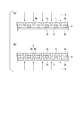
- an elastomer sheet 3 having a support plate 1 therein is prepared.
- the support plate 1 is provided with a plurality of through-holes 2 penetrating in the thickness direction at positions corresponding to the plurality of holding holes 4 to be formed later in the elastomer sheet 3.
- the entire support plate 1 is embedded in the elastomer sheet 3, but a part of the support plate 1, for example, the second surface 1 b of the support plate 1 may be exposed to the outside of the elastomer sheet 3.
- the thickness from the first surface 1a of the support plate 1 to the first surface 3a of the elastomer sheet 3 and the thickness from the second surface 1b of the support plate 1 to the second surface 3b of the elastomer sheet 3 are independent of each other.
- the thickness may be 50 ⁇ m to 2000 ⁇ m.
- the thickness from the first surface 3a to the second surface 3b of the elastomer sheet 3 can be, for example, 200 ⁇ m to 5000 ⁇ m.
- the hole diameter of the through hole 2 provided in the support plate 1 may be larger than the hole diameter (inner diameter) of the holding hole 4 to be formed, and may be, for example, 50 ⁇ m to 5000 ⁇ m.
- the diameters of the through holes 2 may be the same or different.
- the thickness of the support plate 1 can be set to 100 ⁇ m to 5000 ⁇ m, for example.
- the shape of the electronic component holding jig to be formed is likely to be a shape suitable for holding the electronic component.
- the type of elastomer is not particularly limited as long as the holding hole 4 can be formed by laser processing.
- thermosetting elastomers such as silicone rubber and fluororubber; thermoplastics including styrene, olefin, urethane, amide and the like Elastomers; vulcanized rubber and the like.
- thermosetting elastomers such as silicone rubber and fluororubber; thermoplastics including styrene, olefin, urethane, amide and the like Elastomers; vulcanized rubber and the like.
- a thermosetting elastomer is preferable and silicone rubber is more preferable.
- the method for forming the elastomer sheet 3 is not particularly limited, and a known method for forming an elastomer sheet on a substrate is applicable.
- an elastomer sheet can be formed on one surface of the support plate 1 by placing the support plate 1 on a flat base, applying an elastomer composition thereon, and curing the elastomer. At this time, the elastomer is also filled in the through holes provided in the support plate 1 in advance.
- the support plate 1 on the base is turned over and placed again with the other surface exposed, and an elastomer composition is applied to the other surface of the support plate 1 to cure the elastomer,
- a sheet in which the elastomer sheet 3 is formed on both surfaces of the support plate 1, that is, a sheet in which the support plate 1 is provided inside the elastomer sheet 3 is obtained.
- the laser beam L shaped with a mask pattern and further condensed with a lens is irradiated toward the first surface 3a of the elastomer sheet 3 (FIG. 1B).
- the laser beam L is irradiated toward a portion where the through hole 2 of the support plate 1 is provided in advance, and the elastomer sheet 3 is excavated by thermal processing. If excavation is performed until the laser beam L penetrates through the elastomer sheet 3, a penetrating holding hole 4 is formed at the irradiated position (FIG. 1C). Further, if excavation is stopped before the laser beam L penetrates, a non-penetrating holding hole 4 is formed at the irradiated location. Examples of lasers suitable for such processing include pulsed CO 2 lasers and YAG lasers.
- the laser beam emitted from the laser oscillator is selected from a mask pattern having a beam shaping transmission hole, a fly-eye lens, a field lens, an anamorphic beam expander, a concave cylindrical lens, a convex cylindrical lens, a prism, a convex lens, and a concave lens.
- the primary shaping is preferably performed by two or more known optical systems.
- the beam shaped primarily by the mask pattern and the optical system is further shaped secondarily through a mask pattern having a transmission hole corresponding to the shape of the opening of the through hole or the non-through hole formed in the elastomer sheet 3. It is preferable. Specifically, when the mask pattern includes a rectangular transmission hole, the holding hole 4 having a rectangular shape when viewed from above can be formed. If the mask pattern includes a circular transmission hole, the holding hole 4 having a circular shape when viewed from above can be formed.
- the number of transmission holes in the mask pattern may be one or two or more. For example, if the mask pattern has four transmission holes, four holding holes corresponding to the shape of each transmission hole are simultaneously formed in the elastomer sheet 3 by four beams transmitted through the transmission holes of the mask pattern. Can be formed. By forming a plurality of holding holes at the same time, the formation efficiency of the holding holes can be increased.
- the mask pattern is formed of a known material such as a metal such as SUS or ceramics.
- the transmission hole of the mask pattern can be made larger than the holding hole 4 to be formed.
- the beam shaped through the transmission hole of the mask pattern is collected by the lens and can have a beam diameter smaller than that of the transmission hole.
- the beam shaped by the primary shaping or the secondary shaping by the above optical system is further passed through the telecentric lens so that the beam is incident substantially perpendicular to the first surface 3a of the elastomer sheet 3, and is passed through the first surface 3a. It is preferable to form an image.
- the taper angle of the side surface of the holding hole 4 is reduced to form the holding hole 4 having an inner surface substantially perpendicular to the first surface 3a. be able to.
- the taper angle is an angle formed by the inner surface of the holding hole 4 and the perpendicular of the first surface 3a.
- the taper angle is 0 °.
- the beam diameter of the laser light L that has passed through the mask pattern and the lens is preferably equal to the inner diameter of the holding hole 4 to be formed. With this beam diameter, since the entire single holding hole 4 to be formed can be irradiated, it is not necessary to scan the beam when forming the holding hole 4. On the other hand, when irradiating while narrowing the beam diameter and tracing the outline of the holding hole 4, it is necessary to scan the beam with high accuracy, and the manufacturing efficiency is remarkably lowered.
- the angle at which the beam is incident on the first surface 3a of the elastomer sheet 3 may be adjusted by adjusting the lens type, focal point, etc., and a desired taper angle may be given to the inner surface of the holding hole 4.
- a taper angle may be given to all of the inner surface of the holding hole 4, or a taper angle may be attached to a part of the inner surface.
- a taper angle may be given to any one or more of the four inner surfaces in which the cross-sectional shape of the holding hole 4 cut into a circle as described above is rectangular.
- the laser beam L is irradiated from the 1st surface 3a side of the prepared elastomer sheet 3 toward the through-hole 2 of the support plate 1 with which the inside of the elastomer sheet 3 was equipped. Then, the first surface 3a of the elastomer sheet 3 is excavated to form the first hole 4a.
- the excavation of the first surface 3a and the formation of the first hole 4a by the laser beam L and the excavation of the second surface 3b and the formation of the second hole 4b may be performed simultaneously or individually.
- irradiation of the laser beam from the 1st surface 3a side is stopped, and then the laser beam is irradiated from the 2nd surface 3b side, and the 2nd hole 4b is made. Can be formed.
- the laser beam L can be simultaneously irradiated from both the first surface 3a and the second surface 3b of the elastomer sheet 3.
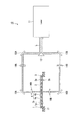
- 3 includes a laser oscillator 11, a right-angle prism mirror 12 for beam branching, first mirrors 13A and 13B, mask patterns 14A and 14B, second mirrors 15A and 15B, lenses 16A and 16A. B and an XY stage 17.
- the laser beam L emitted from the laser oscillator 11 is split into two by the right-angle prism mirror 12.
- the first beam is controlled in direction by the first mirror 13A and shaped by the mask pattern 14A, and then directed to the lens 16A by the second mirror 15A. Further, the light is condensed by the lens 16A and incident on the first surface 3a of the elastomer sheet 3 installed on the XY stage 17, thereby forming a first hole 4a.
- the direction of the second beam is controlled by the first mirror 13B and shaped by the mask pattern 14B, and then directed to the lens 16B by the second mirror 15B. Further, the light is condensed by the lens 16B and incident on the second surface 3b of the elastomer sheet 3 installed on the XY stage 17 to form the second hole 4b.
- the angle at which the laser beam L is incident on the elastomer sheet 3 is adjusted by adjusting the type and focus of the lens, and a desired taper is formed on the inner surface of the holding hole 4. You may add a corner. As shown in FIG. 4B, by reducing the inner diameters of the first hole 4a and the second hole 4b toward the inside, the inner surface protrudes toward the central part 4c of the holding hole 4.
- the holding hole 4 like the inner space of the hourglass can be formed.
- the following surface treatment may be further performed. That is, it is preferable to perform a surface treatment that reduces the adhesiveness to the electronic component P on at least one of the first surface 3 a and the second surface 3 b of the elastomer sheet 3.
- the adhesiveness is tackiness inherently possessed by the elastomer constituting the elastomer sheet 3.
- the method of performing the blast process which sprays microparticles
- the surface treatment may be performed before the holding hole 4 is formed in the elastomer sheet 3 or after the holding hole 4 is formed.
- an electronic component holding jig having an elastomer sheet in which a through hole for holding an electronic component is formed, and the inner diameter of the holding hole is from the first opening edge.
- the electronic component holding jig is reduced in diameter toward the inside and reduced in diameter from the second opening edge toward the inside.
- the electronic component holding jig of the third aspect can be manufactured by the manufacturing method of the first aspect and the second aspect. As an example, there is an electronic component holding jig 20 shown in FIG.
- the electronic component holding jig 20 includes a 20 cm ⁇ 30 cm rectangular support plate 1 and an elastomer sheet 3 having a support plate 1 therein and having a larger volume than the support plate 1. And having.
- the support plate 1 is provided with a plurality of through holes 2 (not shown) arranged in 7 rows ⁇ 13 columns at a pitch of about 2 mm.
- a holding hole 4 having a diameter slightly smaller than the diameter of the through hole 2 is formed inside the through hole 2 at a location where the elastomer sheet 3 covers each through hole 2 of the support plate 1.
- a pitch (separation distance) ⁇ between adjacent holding holes 4 is about 2 mm.
- the inner diameter ⁇ 1 of the first opening edge of the holding hole 4 is the widest and is reduced toward the inside (in the thickness direction of the elastomer sheet 3).
- the inner diameter ⁇ 2 of the second opening edge is the widest, and the diameter is reduced toward the inside.
- the inner diameter ⁇ 3 of the central portion 4c of the holding hole 4 becomes the smallest, and the inner side surface of the holding hole 4 has a taper angle ⁇ that is inclined with respect to the first surface 3a and the second surface 3b of the elastomer sheet 3.
- the opening of the holding hole 4 is relatively wide, so that the electronic component P can be easily inserted.
- the electronic component P can be reliably held in the central portion 4c that is narrow.
- the upper end and the lower end of the electronic component P held in the holding hole 4 protrude from the elastomer sheet 3, and a terminal or the like is attached separately. Thereafter, the electronic component P is extracted from the holding hole 4 and used.
- the shape of the opening of the holding hole 4 when one of the holding holes 4 is viewed from above is appropriately set according to the shape of the electronic component P.
- Examples of the shape include a square and other polygons.
- FIG. 5 illustrates a case of a quadrangle.
- the shape of the opening of the through hole 2 and the shape of the opening of the holding hole 4 are the same square, but the shape of the opening of the through hole 2 and the shape of the opening of the holding hole 4 do not have to be the same. , May be different from each other.
- the inner diameter of the holding hole 4 is appropriately adjusted according to the size of the electronic component P.
- the inner diameters ⁇ 1 and ⁇ 2 of the first opening edge and the second opening edge are 10 ⁇ m to 1000 ⁇ m, and the inner diameter ⁇ 3 of the central portion 4c is 5 to 250 ⁇ m. Size.
- the inner diameter of each portion of the holding hole 4 is the diameter of the smallest circle including the cross-sectional shape of the holding hole 4 perpendicular to the thickness direction of the elastomer sheet 3.
- the length (depth) of the holding hole 4 is the same as the thickness of the elastomer sheet 3, and examples thereof include a size of 500 ⁇ m to 5000 ⁇ m from the first opening edge to the second opening edge.
- the size and shape of each holding hole 4 may be the same or different.
- the pitch between the holding holes 4 is not particularly limited, and can be, for example, about 2 mm to 5 mm.
- the size of the electronic component holding jig 20 is not particularly limited.
- the electronic component holding jig 20 may be a rectangle having a side of 10 cm to 30 cm.
- the size of the support plate 1 is preferably a size that can be embedded in the elastomer sheet 3.
- the through hole 2 is provided at a position corresponding to the holding hole 4, and therefore the through hole 2 is arranged so as to surround the holding hole 4.
- the electronic component P or the manipulator (operation tool) of the electronic component contacts the elastomer sheet 3 when the electronic component P is inserted or removed. Even if it does, since the electronic component P or the manipulator is hard to adhere to the surface of the elastomer sheet 3, it is preferable because the electronic component P can be more easily inserted and removed.
- SYMBOLS 1 Support plate, 1a ... 1st surface, 1b ... 2nd surface, 2 ... Through-hole, 3 ... Elastomer sheet, 3a ... 1st surface, 3b ... 2nd surface, 4 ... Holding hole, 4a ... 1st hole ( Upper part of holding hole), 4b ... Second hole (lower part of holding hole), 4c ... Central part of holding hole, P ... Electronic component, L ... Laser beam (laser beam), 10 ... Laser processing device, 11 ... Laser oscillator , 12 ... right angle prism mirror, 13A, B ... first mirror, 14A, B ... mask pattern, 15A, B ... second mirror, 16A, B ... lens, 17 ... XY stage
Landscapes
- Engineering & Computer Science (AREA)
- Physics & Mathematics (AREA)
- Optics & Photonics (AREA)
- Plasma & Fusion (AREA)
- Mechanical Engineering (AREA)
- Power Engineering (AREA)
- Manufacturing & Machinery (AREA)
- Microelectronics & Electronic Packaging (AREA)
- Laser Beam Processing (AREA)
- Fixed Capacitors And Capacitor Manufacturing Machines (AREA)
Abstract
Description
本願は、2016年11月9日に、日本に出願された特願2016-218585号に基づき優先権を主張し、その内容をここに援用する。
このような電子部品保持治具を製造する方法としては、金型内において、基板に形成された複数の貫通孔内にそれよりも小径なピンをそれぞれ配置し、ピンを貫通させた状態で、金型内に未硬化の弾性体材料液を流し込み、弾性体をシート状に硬化させた後、ピンを取り除くことで、保持穴を形成する方法が適用されている(特許文献1参照)。
[2] 前記エラストマーシートの内部には支持板が備えられ、前記支持板には、
前記エラストマーシートに形成する前記保持穴に対応する位置に貫通孔が予め設けられており、前記エラストマーシートの第一面側から、前記支持板の前記貫通孔へ向けて前記レーザー光を照射して、前記エラストマーシートの第一面を掘削して第一穴を形成し、前記エラストマーシートの第二面側から、前記支持板の前記貫通孔へ向けて前記レーザー光を照射して、前記エラストマーシートの第二面を掘削して第二穴を形成し、前記エラストマーシートの内部において、前記第一穴と前記第二穴とを連結することによって貫通した前記保持穴を形成する、[1]に記載の電子部品保持治具の製造方法。
[3] 前記第一穴及び前記第二穴の内径がそれぞれ内部へ向かって縮径している、[2]に記載の電子部品保持治具の製造方法。
[4] 前記レーザー光はCO2レーザーであり、前記レンズはテレセントリックレンズであり、前記マスクパターンが有する前記透過孔は2つ以上である、[1]~[3]の何れか一項に記載の電子部品保持治具の製造方法。
[5] 前記エラストマーシートの第一面及び第二面の少なくとも一方に対して、前記電子部品に対する粘着性を低減させる表面処理を行う、[1]~[4]の何れか一項に記載の電子部品保持治具の製造方法。
[6] 電子部品を保持するための貫通した保持穴が形成されたエラストマーシートを有する電子部品保持治具であって、前記保持穴の内径は、その第一の開口縁から内部へ向けて縮径しているとともに、その第二の開口縁から内部へ向けて縮径していることを特徴とする電子部品保持治具。
[7] 前記エラストマーシートの表面が、前記電子部品に対する粘着性が低減するように表面処理されている、[6]に記載の電子部品保持治具。
本発明の電子部品保持治具によれば、保持穴が有する独特の形状によって、保持穴の内部に電子部品を安定に保持することができる。
(第一態様)
本発明の第一態様は、エラストマーシートに対してレーザー光を照射することにより、前記エラストマーシートに、電子部品を保持するための貫通の又は非貫通の保持穴を形成する、電子部品保持治具の製造方法である。レーザー光の照射は、レーザー発振器から出射したレーザー光を、形成する保持穴の形状に対応する透過孔を有するマスクパターンに通し、さらにレンズで集光した後、前記エラストマーシートに照射する方法で行う。
エラストマーシート3の第一面3aから第二面3bまでの厚さは、例えば、200μm~5000μmとすることができる。
支持板1に設けられた貫通孔2の孔径は、形成する保持穴4の穴径(内径)よりも大きければよく、例えば、50μm~5000μmとすることができる。各貫通孔2の孔径は互いに同じであってもよいし、異なっていてもよい。
支持板1の厚さは、例えば、100μm~5000μmとすることができる。
支持板1、貫通孔2及びエラストマーシート3が上記の各寸法であると、形成する電子部品保持治具の形状が電子部品の保持に適した形状になり易い。
このような加工に適したレーザーとしては、パルス発振のCO2レーザー、YAGレーザーなどが挙げられる。
本発明の第二態様は、第一態様と同様に、前記エラストマーシートに形成する前記保持穴に対応する位置に貫通孔が予め設けられた支持板を内部に備えた、エラストマーシートを準備し、前記エラストマーシートの第一面側から、前記支持板の前記貫通孔へ向けて前記レーザー光を照射して、前記エラストマーシートの第一面を掘削して第一穴を形成し、前記エラストマーシートの第二面側から、前記支持板の前記貫通孔へ向けて前記レーザー光を照射して、前記エラストマーシートの第二面を掘削して第二穴を形成し、前記エラストマーシートの内部において、前記第一穴と前記第二穴とを連結することによって、目的の前記保持穴を形成する、電子部品保持治具の製造方法である。
以上で説明した本発明の電子部品保持治具の製造方法によれば、高価な金型を用いずに、比較的安価なマスクパターンを用いて保持穴を形成できる。このため、製造コストが低減するとともに、保持穴の寸法変更を迅速に行うことができる。また、エラストマーシートの成形と、保持穴の形成を別工程で行うため、エラストマーシートの成形時に保持穴が収縮する懸念がなく、高い精度で容易に保持穴を形成することができる。
前記表面処理は、エラストマーシート3に保持穴4を形成する前に行ってもよいし、保持穴4を形成した後に行ってもよい。
本発明の第三態様は、電子部品を保持するための貫通した保持穴が形成されたエラストマーシートを有する電子部品保持治具であって、前記保持穴の内径は、その第一の開口縁から内部へ向けて縮径しているとともに、その第二の開口縁から内部へ向けて縮径している電子部品保持治具である。第三態様の電子部品保持治具は、第一態様及び第二態様の製造方法によって製造することができる。一例として、図4に示す電子部品保持治具20が挙げられる。
図5の例では、貫通孔2の開口の形状と保持穴4の開口の形状は同じ四角形であるが、貫通孔2の開口の形状と保持穴4の開口の形状は同じである必要は無く、互いに異なっていてもよい。
エラストマーシート3に設けられる保持穴4の個数、配置は特に限定されず、例えば2×2=4個~100×100=1万個のグリッド配列が挙げられる。また、各保持穴4のサイズや形状は同じであってもよいし、異なっていてもよい。
保持穴4同士のピッチは特に限定されず、例えば、2mm~5mm程度とすることができる。電子部品保持治具20のサイズは特に限定されず、例えば、一辺が10cm~30cmの矩形とすることができる。
Claims (7)
- エラストマーシートに対してレーザー光を照射することにより、前記エラストマーシートに電子部品を保持するための保持穴を形成する、電子部品保持治具の製造方法であって、
レーザー発振器から出射したレーザー光を、形成する前記保持穴の形状に対応する透過孔を有するマスクパターンに通し、さらにレンズで集光した後、前記エラストマーシートに照射することを特徴とする電子部品保持治具の製造方法。 - 前記エラストマーシートの内部には支持板が備えられ、
前記支持板には、前記エラストマーシートに形成する前記保持穴に対応する位置に貫通孔が予め設けられており、
前記エラストマーシートの第一面側から、前記支持板の前記貫通孔へ向けて前記レーザー光を照射して、前記エラストマーシートの第一面を掘削して第一穴を形成し、
前記エラストマーシートの第二面側から、前記支持板の前記貫通孔へ向けて前記レーザー光を照射して、前記エラストマーシートの第二面を掘削して第二穴を形成し、
前記エラストマーシートの内部において、前記第一穴と前記第二穴とを連結することによって貫通した前記保持穴を形成する、請求項1に記載の電子部品保持治具の製造方法。 - 前記第一穴及び前記第二穴の内径がそれぞれ内部へ向かって縮径している、請求項2に記載の電子部品保持治具の製造方法。
- 前記レーザー光はCO2レーザーであり、前記レンズはテレセントリックレンズであり、前記マスクパターンが有する前記透過孔は2つ以上である、請求項1~3の何れか一項に記載の電子部品保持治具の製造方法。
- 前記エラストマーシートの第一面及び第二面の少なくとも一方に対して、前記電子部品に対する粘着性を低減させる表面処理を行う、請求項1~4の何れか一項に記載の電子部品保持治具の製造方法。
- 電子部品を保持するための貫通した保持穴が形成されたエラストマーシートを有する電子部品保持治具であって、
前記保持穴の内径は、その第一の開口縁から内部へ向けて縮径しているとともに、その第二の開口縁から内部へ向けて縮径していることを特徴とする電子部品保持治具。 - 前記エラストマーシートの表面が、前記電子部品に対する粘着性が低減するように加工されている、請求項6に記載の電子部品保持治具。
Priority Applications (3)
| Application Number | Priority Date | Filing Date | Title |
|---|---|---|---|
| KR1020197012124A KR20190073398A (ko) | 2016-11-09 | 2017-11-01 | 전자 부품 유지 지그 및 그 제조 방법 |
| JP2018550164A JPWO2018088299A1 (ja) | 2016-11-09 | 2017-11-01 | 電子部品保持治具及びその製造方法 |
| US16/344,788 US20190337090A1 (en) | 2016-11-09 | 2017-11-01 | Electronic component holding jig, and method for manufacturing said electronic component holding jig |
Applications Claiming Priority (2)
| Application Number | Priority Date | Filing Date | Title |
|---|---|---|---|
| JP2016-218585 | 2016-11-09 | ||
| JP2016218585 | 2016-11-09 |
Publications (1)
| Publication Number | Publication Date |
|---|---|
| WO2018088299A1 true WO2018088299A1 (ja) | 2018-05-17 |
Family
ID=62110260
Family Applications (1)
| Application Number | Title | Priority Date | Filing Date |
|---|---|---|---|
| PCT/JP2017/039545 Ceased WO2018088299A1 (ja) | 2016-11-09 | 2017-11-01 | 電子部品保持治具及びその製造方法 |
Country Status (5)
| Country | Link |
|---|---|
| US (1) | US20190337090A1 (ja) |
| JP (1) | JPWO2018088299A1 (ja) |
| KR (1) | KR20190073398A (ja) |
| TW (1) | TWI659792B (ja) |
| WO (1) | WO2018088299A1 (ja) |
Cited By (1)
| Publication number | Priority date | Publication date | Assignee | Title |
|---|---|---|---|---|
| JP2023098795A (ja) * | 2021-12-29 | 2023-07-11 | サムソン エレクトロ-メカニックス カンパニーリミテッド. | セラミック電子部品の製造方法 |
Families Citing this family (1)
| Publication number | Priority date | Publication date | Assignee | Title |
|---|---|---|---|---|
| JP7782479B2 (ja) * | 2023-01-20 | 2025-12-09 | 株式会社村田製作所 | 電子部品の製造方法及び電子部品保持治具 |
Citations (5)
| Publication number | Priority date | Publication date | Assignee | Title |
|---|---|---|---|---|
| JPS4726792B1 (ja) * | 1969-03-11 | 1972-07-19 | ||
| JPH0214508A (ja) * | 1989-05-01 | 1990-01-18 | Murata Mfg Co Ltd | チップ部品の保持プレートの製造方法 |
| JPH11347766A (ja) * | 1998-06-02 | 1999-12-21 | Sumitomo Heavy Ind Ltd | レーザドリル装置及びレーザ穴あけ加工方法 |
| JP2006502006A (ja) * | 2002-10-04 | 2006-01-19 | エレクトロ サイエンティフィック インダストリーズ インコーポレーテッド | 超小型部品用搬送具の弾性マスクに正確な寸法のスロットを形成する方法 |
| JP2015002268A (ja) * | 2013-06-14 | 2015-01-05 | 信越ポリマー株式会社 | 保持治具 |
Family Cites Families (1)
| Publication number | Priority date | Publication date | Assignee | Title |
|---|---|---|---|---|
| JP3147418B2 (ja) | 1991-08-09 | 2001-03-19 | 株式会社日立製作所 | Mri用rfコイル |
-
2017
- 2017-11-01 WO PCT/JP2017/039545 patent/WO2018088299A1/ja not_active Ceased
- 2017-11-01 KR KR1020197012124A patent/KR20190073398A/ko not_active Ceased
- 2017-11-01 JP JP2018550164A patent/JPWO2018088299A1/ja active Pending
- 2017-11-01 US US16/344,788 patent/US20190337090A1/en not_active Abandoned
- 2017-11-02 TW TW106137896A patent/TWI659792B/zh active
Patent Citations (5)
| Publication number | Priority date | Publication date | Assignee | Title |
|---|---|---|---|---|
| JPS4726792B1 (ja) * | 1969-03-11 | 1972-07-19 | ||
| JPH0214508A (ja) * | 1989-05-01 | 1990-01-18 | Murata Mfg Co Ltd | チップ部品の保持プレートの製造方法 |
| JPH11347766A (ja) * | 1998-06-02 | 1999-12-21 | Sumitomo Heavy Ind Ltd | レーザドリル装置及びレーザ穴あけ加工方法 |
| JP2006502006A (ja) * | 2002-10-04 | 2006-01-19 | エレクトロ サイエンティフィック インダストリーズ インコーポレーテッド | 超小型部品用搬送具の弾性マスクに正確な寸法のスロットを形成する方法 |
| JP2015002268A (ja) * | 2013-06-14 | 2015-01-05 | 信越ポリマー株式会社 | 保持治具 |
Cited By (1)
| Publication number | Priority date | Publication date | Assignee | Title |
|---|---|---|---|---|
| JP2023098795A (ja) * | 2021-12-29 | 2023-07-11 | サムソン エレクトロ-メカニックス カンパニーリミテッド. | セラミック電子部品の製造方法 |
Also Published As
| Publication number | Publication date |
|---|---|
| TWI659792B (zh) | 2019-05-21 |
| US20190337090A1 (en) | 2019-11-07 |
| KR20190073398A (ko) | 2019-06-26 |
| JPWO2018088299A1 (ja) | 2019-07-11 |
| TW201822932A (zh) | 2018-07-01 |
Similar Documents
| Publication | Publication Date | Title |
|---|---|---|
| US20130078821A1 (en) | Imprint method, imprint apparatus, and manufacturing method of semiconductor device | |
| JP6200135B2 (ja) | インプリント装置、インプリント方法、および、物品製造方法 | |
| JP2011508253A (ja) | 光学要素の製造 | |
| JP6837905B2 (ja) | ウエーハの加工方法 | |
| JP2008247022A (ja) | 微細パターン形成方法、この微細パターン形成方法によって形成される型、この型を用いた転写方法および微細パターン形成方法 | |
| TWI610088B (zh) | 截頂型鏡片,截頂型鏡片對及相應裝置的製造方法 | |
| CN108067746B (zh) | 基板的加工方法 | |
| KR20130058011A (ko) | 레이저 가공 장치 | |
| CN104105569A (zh) | 用于在介电基片中形成精细尺度结构的方法和设备 | |
| TWI673239B (zh) | 微孔陣列及其製造方法 | |
| WO2018088299A1 (ja) | 電子部品保持治具及びその製造方法 | |
| US20220204393A1 (en) | Method for manufacturing glass sheet, and glass sheet and glass sheet assembly | |
| JP6050002B2 (ja) | レーザ加工方法 | |
| WO2016199659A1 (ja) | 基板一体型ガスケットの製造方法 | |
| US20180134607A1 (en) | Substrate processing method | |
| KR100815361B1 (ko) | 인쇄회로기판의 제조방법 | |
| JP2015115526A (ja) | チャックテーブルの成形方法 | |
| KR20220058671A (ko) | 나노구조를 엠보싱하기 위한 방법 및 장치 | |
| US6215098B1 (en) | Method for manufacturing a holding tray for chip components | |
| TWI753169B (zh) | 加工對象物切斷方法 | |
| JP4756339B2 (ja) | 微細構造転写方法、微細構造転写装置及び光学素子製造方法 | |
| CN111063646B (zh) | 晶片保持装置和使用了晶片保持装置的晶片的加工方法 | |
| JP6875233B2 (ja) | テンプレート基板、テンプレート基板の製造方法、及び半導体装置の製造方法 | |
| CN111246989B (zh) | 复制的改进以及相关方法和装置,特别是用于最小化不对称形式误差 | |
| JPH0997967A (ja) | フレキシブルプリント配線板の製造方法 |
Legal Events
| Date | Code | Title | Description |
|---|---|---|---|
| 121 | Ep: the epo has been informed by wipo that ep was designated in this application |
Ref document number: 17869713 Country of ref document: EP Kind code of ref document: A1 |
|
| ENP | Entry into the national phase |
Ref document number: 2018550164 Country of ref document: JP Kind code of ref document: A |
|
| ENP | Entry into the national phase |
Ref document number: 20197012124 Country of ref document: KR Kind code of ref document: A |
|
| NENP | Non-entry into the national phase |
Ref country code: DE |
|
| 122 | Ep: pct application non-entry in european phase |
Ref document number: 17869713 Country of ref document: EP Kind code of ref document: A1 |