WO2018074301A1 - 光送信装置および光通信システム - Google Patents
光送信装置および光通信システム Download PDFInfo
- Publication number
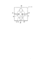
- WO2018074301A1 WO2018074301A1 PCT/JP2017/036821 JP2017036821W WO2018074301A1 WO 2018074301 A1 WO2018074301 A1 WO 2018074301A1 JP 2017036821 W JP2017036821 W JP 2017036821W WO 2018074301 A1 WO2018074301 A1 WO 2018074301A1
- Authority
- WO
- WIPO (PCT)
- Prior art keywords
- core
- optically coupled
- light
- mode
- emitting unit
- Prior art date
- Legal status (The legal status is an assumption and is not a legal conclusion. Google has not performed a legal analysis and makes no representation as to the accuracy of the status listed.)
- Ceased
Links
Images







Classifications
-
- H—ELECTRICITY
- H01—ELECTRIC ELEMENTS
- H01S—DEVICES USING THE PROCESS OF LIGHT AMPLIFICATION BY STIMULATED EMISSION OF RADIATION [LASER] TO AMPLIFY OR GENERATE LIGHT; DEVICES USING STIMULATED EMISSION OF ELECTROMAGNETIC RADIATION IN WAVE RANGES OTHER THAN OPTICAL
- H01S5/00—Semiconductor lasers
- H01S5/02—Structural details or components not essential to laser action
- H01S5/022—Mountings; Housings
- H01S5/0239—Combinations of electrical or optical elements
-
- G—PHYSICS
- G02—OPTICS
- G02B—OPTICAL ELEMENTS, SYSTEMS OR APPARATUS
- G02B6/00—Light guides; Structural details of arrangements comprising light guides and other optical elements, e.g. couplings
- G02B6/02—Optical fibres with cladding with or without a coating
-
- G—PHYSICS
- G02—OPTICS
- G02B—OPTICAL ELEMENTS, SYSTEMS OR APPARATUS
- G02B6/00—Light guides; Structural details of arrangements comprising light guides and other optical elements, e.g. couplings
- G02B6/10—Light guides; Structural details of arrangements comprising light guides and other optical elements, e.g. couplings of the optical waveguide type
- G02B6/12—Light guides; Structural details of arrangements comprising light guides and other optical elements, e.g. couplings of the optical waveguide type of the integrated circuit kind
- G02B6/122—Basic optical elements, e.g. light-guiding paths
- G02B6/125—Bends, branchings or intersections
-
- G—PHYSICS
- G02—OPTICS
- G02B—OPTICAL ELEMENTS, SYSTEMS OR APPARATUS
- G02B6/00—Light guides; Structural details of arrangements comprising light guides and other optical elements, e.g. couplings
- G02B6/24—Coupling light guides
- G02B6/26—Optical coupling means
-
- G—PHYSICS
- G02—OPTICS
- G02B—OPTICAL ELEMENTS, SYSTEMS OR APPARATUS
- G02B6/00—Light guides; Structural details of arrangements comprising light guides and other optical elements, e.g. couplings
- G02B6/24—Coupling light guides
- G02B6/42—Coupling light guides with opto-electronic elements
-
- H—ELECTRICITY
- H01—ELECTRIC ELEMENTS
- H01S—DEVICES USING THE PROCESS OF LIGHT AMPLIFICATION BY STIMULATED EMISSION OF RADIATION [LASER] TO AMPLIFY OR GENERATE LIGHT; DEVICES USING STIMULATED EMISSION OF ELECTROMAGNETIC RADIATION IN WAVE RANGES OTHER THAN OPTICAL
- H01S5/00—Semiconductor lasers
- H01S5/40—Arrangement of two or more semiconductor lasers, not provided for in groups H01S5/02 - H01S5/30
- H01S5/42—Arrays of surface emitting lasers
-
- H—ELECTRICITY
- H04—ELECTRIC COMMUNICATION TECHNIQUE
- H04J—MULTIPLEX COMMUNICATION
- H04J14/00—Optical multiplex systems
- H04J14/04—Mode multiplex systems
-
- H—ELECTRICITY
- H04—ELECTRIC COMMUNICATION TECHNIQUE
- H04J—MULTIPLEX COMMUNICATION
- H04J14/00—Optical multiplex systems
- H04J14/05—Spatial multiplexing systems
- H04J14/052—Spatial multiplexing systems using multicore fibre
-
- H—ELECTRICITY
- H10—SEMICONDUCTOR DEVICES; ELECTRIC SOLID-STATE DEVICES NOT OTHERWISE PROVIDED FOR
- H10F—INORGANIC SEMICONDUCTOR DEVICES SENSITIVE TO INFRARED RADIATION, LIGHT, ELECTROMAGNETIC RADIATION OF SHORTER WAVELENGTH OR CORPUSCULAR RADIATION
- H10F77/00—Constructional details of devices covered by this subclass
- H10F77/40—Optical elements or arrangements
Definitions
- the present invention relates to an optical transmission device and an optical communication system.
- This application claims priority based on Japanese Patent Application No. 2016-207302 filed in Japan on October 21, 2016, the contents of which are incorporated herein by reference.
- WDM wavelength division multiplexing method
- a wavelength tunable laser is used to change the wavelength for each transceiver and multiplex the wavelength. It was.
- the communication capacity of WDM is insufficient, and as described in Patent Document 1 and Non-Patent Document 1, research using mode multiplexing is being performed.
- Patent Document 1 and Non-Patent Document 1 optical transmission using a method in which a fundamental mode and a higher-order mode are excited using a mode multiplexer / demultiplexer and are incident on an optical fiber in order to multiplex transverse modes in an optical fiber.
- a device has been proposed.
- Patent Document 2 in an optical transmission device using a VCSEL, single-mode light is incident on an optical fiber with a spatial optical angle using an optical element such as a lens. The mode is multiplexed by adjusting.
- An object of one embodiment of the present invention is to provide an optical transmission device and an optical communication system that have a simple structure and can be reduced in size and price.
- An optical transmission apparatus includes a light source, a directional coupler, and an optical transmission line having a transmission line core optically coupled to the directional coupler, wherein the light source includes at least A first light-emitting unit that emits first light including a fundamental mode; and a second light-emitting unit that emits second light including a higher-order mode higher in order than the basic mode, and the directional coupler is A first waveguide region having at least a first core optically coupled to the first light emitting unit and disposed to be optically coupled to the transmission line core, and at least a part of the higher-order mode is transitioned A second waveguide region having a second core and a third core formed so as to be optically coupled to each other, and one of the second core and the third core is the first core So that it is optically coupled to the two light emitting parts and not optically coupled to the transmission line core.
- a fourth core formed at a distance from the first core so that the first waveguide region is optically coupled to the first core so that at least a part of the higher-order mode can be transitioned.
- the fourth core may be arranged so as not to be optically coupled to the first light emitting unit and to be optically coupled to the transmission line core.
- the light source is a surface emitting laser
- each of the first light emitting unit and the second light emitting unit includes at least an active layer having a multiple quantum well structure and a current confinement layer having an opening
- An inner diameter of the opening of the current confinement layer of the two light emitting portions may be larger than an inner diameter of the opening of the current confinement layer of the first light emitting portion.
- the optical transmission line may be a graded index optical fiber.
- the directional coupler may be a multi-core optical fiber having the first core, the second core, and the third core.
- An optical communication system includes the optical transmission device and a reception unit optically coupled to the optical transmission device, wherein the reception unit is optically coupled to the optical transmission path.
- a signal photoelectrically converted by the first light receiving unit or the second light receiving unit downstream of the first light receiving unit or the second light receiving unit on which the higher-order mode is incident a signal photoelectrically converted by the first light receiving unit or the second light receiving unit downstream of the first light receiving unit or the second light receiving unit on which the higher-order mode is incident.
- An electrical low cut filter for removing a part of the filter may be provided.
- An optical transmission device includes a light source, a directional coupler, and an optical transmission line having a transmission line core optically coupled to the directional coupler, wherein the light source includes at least A first light-emitting unit that emits first light including a fundamental mode; and a second light-emitting unit that emits second light including a higher-order mode higher in order than the basic mode, and the directional coupler is A first waveguide region having a first core and a fourth core formed at an interval such that at least a part of the fundamental mode is optically coupled to each other in a transitional manner; and at least a part of the higher-order mode And a second waveguide region having a second core and a third core formed so as to be optically coupled to each other so as to be capable of transition, wherein the first core is optically coupled to the first light emitting unit.
- the fourth core is optically coupled to the first light emitting unit and is not optically coupled to the transmission line core, and one of the second core and the third core is connected to the second light emitting unit. It is arranged so as to be optically coupled and not optically coupled to the transmission line core, and the other of the second core and the third core is not optically coupled to the second light emitting unit and light is not incident on the transmission line core. Arranged to be combined.
- the second core and the third core of the second waveguide region are optically coupled so that a part of the higher-order mode can transition.
- one of the second core and the third core is arranged so as to be optically coupled to the transmission line core of the optical transmission line, a higher-order mode transitioned from the other is emitted to the optical transmission line core.
- the first mode of the first light from the first light emitting unit is modulated independently of the first light without using a component for obtaining a plurality of modes separately from the light emitting unit.
- Mode multiplex communication using two higher-order modes of light is possible. Therefore, the structure of the optical transmitter capable of mode multiplexing communication can be simplified, and the size and price can be reduced.
- FIG. 1 It is a block diagram of the receiving part of the optical communication system of FIG. It is a block diagram of the optical transmitter of the optical communication system of 2nd Embodiment. It is sectional drawing of the directional coupler used for the optical transmitter of FIG. It is a figure which shows the example of a low cut filter.
- FIG. 1 is a configuration diagram of an optical communication system 10 according to the first embodiment.
- FIG. 2 is a configuration diagram of the optical transmission device 4 of the optical communication system 10.
- FIG. 3 is a plan view of the light source 11 used in the optical transmission device 4.
- FIG. 4 is a cross-sectional view of the light source 11 along the thickness direction of the substrate 14 described later.
- FIG. 5 is a cross-sectional view of the directional coupler 12 used in the optical transmission device 4.
- the optical communication system 10 includes an optical transmission device 4 and a reception unit 3 optically coupled to the optical transmission device 4.
- the optical transmission device 4 includes a transmission unit 1 and an optical transmission path 2 optically coupled to the transmission unit 1.
- the light source (the first light emitting unit or the second light emitting unit) and the waveguide region core (any one of the first to fourth cores) are optically coupled. It is incident on the wave domain core.
- the light source and the waveguide region core are optically coupled.
- the light source and the waveguide region core are separated from each other, and the light emitted from the light source is incident on the waveguide region core.
- the light source and the waveguide region core are separated from each other, the light source and the waveguide region core are connected to each other through a relay optical transmission line such as an optical fiber, and light emitted from the light source passes through the relay optical transmission line.
- a relay optical transmission line such as an optical fiber
- the light source and the waveguide region core are installed in contact with each other, and the light emitted from the light source enters the waveguide region core.
- the optical coupling between the waveguide region core (any of the first to fourth cores) and the optical transmission line core means that, for example, light emitted from the waveguide region core enters the optical transmission line core.
- two cores are optically coupled so that at least a part of light can transition, for example, one of the two cores That at least part of the light propagating through can be transferred to the other core.
- the optical coupling between the optical transmission line core and the main core of the mode separator means, for example, that light emitted from the optical transmission line core enters the main core.
- the main core or the separation core of the mode separator is optically coupled to the light receiving unit (the first light receiving unit or the second light receiving unit), for example, light emitted from the main core or the separation core is transmitted to the light receiving unit.
- the transmission unit 1 side is referred to as an upstream side
- the reception unit 3 side is referred to as a downstream side.
- the transmission unit 1 includes a light source 11 and a directional coupler 12.
- the light source 11 is, for example, a surface emitting laser (VCSEL: Vertical Cavity Surface Emitting Laser).
- VCSEL Vertical Cavity Surface Emitting Laser
- the light source 11 includes a base portion 6, and a first light emitting portion 7 and a second light emitting portion 8 provided on the base portion 6.
- the base portion 6 is configured by laminating a cathode electrode 13, a substrate 14, and a first mirror layer 15 in this order.
- the cathode electrode 13 is provided on the outer surface of the substrate 14 (the lower surface in FIG. 4).
- an n-type GaAs substrate can be used as the substrate 14.
- the first mirror layer 15 is, for example, an n-type semiconductor layer, and is a distributed Bragg reflection type (DBR mirror) in which low refractive index layers and high refractive index layers are alternately stacked.
- DBR mirror distributed Bragg reflection type
- the 1st light emission part 7 and the 2nd light emission part 8 are arrange
- the plan view means viewing from the thickness direction of the substrate 14.
- the first light emitting unit 7 is configured by laminating an active layer 16A, a current confinement layer 17A, a second mirror layer 18A, a passivation layer 19A, and an anode electrode 20A in this order from the base unit 6.
- the second light emitting unit 8 is configured by laminating an active layer 16B, a current confinement layer 17B, a second mirror layer 18B, a passivation layer 19B, and an anode electrode 20B in this order from the base unit 6.
- the active layers 16A and 16B have a multiple quantum well structure including a plurality of quantum well structures each including, for example, a quantum well layer and a barrier layer.
- the current confinement layers 17A and 17B are obtained by oxidizing an AlAs layer, for example, and have openings 17Aa and 17Ba, respectively.
- the second mirror layers 18A and 18B are p-type semiconductor layers, for example, and are distributed Bragg reflection types (DBR mirrors) in which low refractive index layers and high refractive index layers are alternately stacked.
- DBR mirrors distributed Bragg reflection types
- the passivation layer 19A is formed so as to surround the second mirror layer 18A, for example.
- the passivation layer 19A has an opening 19Aa surrounding at least the opening 17Aa of the current confinement layer 17A in plan view. Note that the plan view means viewing from the thickness direction of the substrate 14.
- the anode electrode 20A is provided so as to surround the passivation layer 19A and the second mirror layer 18A.
- the anode electrode 20A has an opening 20Aa surrounding the opening 17Aa of the current confinement layer 17A in plan view.
- 1st light L1 (refer FIG. 2) is radiate
- the passivation layer 19B is formed, for example, surrounding the second mirror layer 18B.
- the passivation layer 19B has an opening 19Ba surrounding at least the opening 17Ba of the current confinement layer 17B in plan view.
- the anode electrode 20B is provided so as to surround the passivation layer 19B and the second mirror layer 18B.
- the anode electrode 20B has an opening 20Ba surrounding the opening 17Ba of the current confinement layer 17B in plan view.
- 2nd light emission part 8 2nd light L2 (refer FIG. 2) is radiate
- the pair of anode electrode terminals 21 shown in FIG. 3 are connected to the anode electrodes 20A and 20B shown in FIG.
- Each of the pair of cathode electrode terminals 22 shown in FIG. 3 is connected to the cathode electrode 13 shown in FIG.
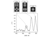
- FIG. 6 is a diagram illustrating an example of a spectrum of light emitted from the second light emitting unit 8.
- the light includes a plurality of modes having different transverse mode orders.
- the light includes a fundamental mode (LP01 mode) having the longest wavelength and a higher-order mode (LP11 mode and LP12 mode) having a higher order than the fundamental mode.
- LP01 mode fundamental mode
- LP11 mode and LP12 mode higher-order mode
- the LP mode linearly polarized polarized propagation mode
- the LP mode may be used when expressing the order of the horizontal mode.
- the peak wavelength of the LP11 mode is shorter than the peak wavelength of the LP01 mode.
- the peak wavelength of the LP12 mode is shorter than the peak wavelength of the LP11 mode.
- the inner diameters Da and Db of the openings 17Aa and 17Ba of the current confinement layers 17A and 17B affect the ratio between the fundamental mode and the higher-order mode included in the light emitted from the light emitting units 7 and 8. For example, as the inner diameters Da and Db of the openings 17Aa and 17Ba are smaller, the ratio of the basic mode to the whole tends to increase. In addition, as the inner diameters Da and Db of the openings 17Aa and 17Ba are larger, the ratio of higher-order modes in the whole tends to increase. Therefore, the ratio between the basic mode and the higher order mode can be adjusted by selecting the inner diameters Da and Db of the openings 17Aa and 17Ba.
- the ratio between the fundamental mode and the higher-order mode is different because the inner diameter Da of the opening 17Aa of the first light emitting unit 7 and the inner diameter Db of the opening 17Ba of the second light emitting unit 8 are different.
- Light L1 and second light L2 are obtained.
- the inner diameter Db of the opening 17Ba of the second light emitting unit 8 is set to be larger than the inner diameter Da of the opening 17Aa of the first light emitting unit 7, higher order modes (for example, LP11 mode and LP12 in the second light L2). Mode) ratio can be made larger than the ratio of the higher-order mode in the first light L1.
- the inner diameter Da of the opening 17Aa of the first light emitting unit 7 is, for example, 5.5 to 6.5 ⁇ m.
- the inner diameter Db of the opening 17Ba of the second light emitting unit 8 is, for example, 8 to 10 ⁇ m.
- the bias current in the light source 11 affects the ratio between the fundamental mode and the higher order mode of the emitted light.
- the basic mode ratio is large at a low current value of about 3 mA from the threshold value Ith, and the high-order mode ratio is large at a high current value of about 9 mA. That is, as the current value of the bias current in the light source 11 is increased, the higher-order mode ratio increases. Therefore, the ratio between the fundamental mode and the higher order mode can be adjusted by the bias current.
- the bias currents in the first light emitting unit 7 and the second light emitting unit 8 are appropriately set, the ratio of the higher order mode in the second light L2 is made larger than the ratio of the higher order mode in the first light L1. be able to.
- the first light emitting unit 7 emits first light L1 including at least a fundamental mode (LP01 mode). Most of the first light L1 is preferably in the fundamental mode. When most of the first light L1 is in the fundamental mode, noise during optical transmission on the optical transmission path 2 can be reduced.
- the second light emitting unit 8 emits second light L2 including at least a higher-order mode.
- the second light L2 may include a fundamental mode and a higher order mode. Higher order modes are, for example, LP11 mode and LP12 mode. When the ratio of the higher-order mode in the second light L2 is large, noise during optical transmission in the optical transmission path 2 can be reduced.
- the directional coupler 12 includes a first waveguide region 26, a second waveguide region 27, and a cladding 25.
- the clad 25 surrounds the first waveguide region 26 and the second waveguide region 27.
- the directional coupler 12 extends from the light source 11 toward the optical transmission line 2.
- the first waveguide region 26 has a first core 28A.
- the first core 28A extends along the longitudinal direction in which the directional coupler 12 extends.
- the second waveguide region 27 has a second core 29A and a third core 29B.
- the second core 29 ⁇ / b> A and the third core 29 ⁇ / b> B extend along the longitudinal direction of the directional coupler 12.
- the second core 29 ⁇ / b> A and the third core 29 ⁇ / b> B are formed in parallel with each other at an interval that enables optical coupling.
- the second core 29A and the third core 29B are formed at an interval at which at least a part of the higher-order mode is optically coupled so that transition is possible.
- a multi-core optical fiber having cores 28A, 29A, 29B and a clad 25 surrounding the cores 28A, 29A, 29B can be used.
- the multi-core optical fiber is preferably a step index (SI) type.
- Two or more of the first core 28A, the second core 29A, and the third core 29B may have the same configuration (for example, material, outer diameter, etc.), or may have different configurations.
- the second core 29A and the first core 28A may have the same configuration or different configurations.
- FIG. 7 shows a directional coupler 12 having a pair of cores (second core 29A and third core 29B).
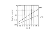
- the distance d (horizontal axis) between the second core 29A and the third core 29B and the coupling length (vertical). It is a figure which shows the example of a relationship with an axis
- FIG. 8 is a diagram illustrating an example of the relationship between the center distance d (horizontal axis) and the remaining power (vertical axis) of the LP01 mode in the second core 29A.
- the second core 29A and the third core 29B had a diameter of 8 ⁇ m and a relative refractive index difference of 0.3%.
- the wavelength of the incident light was 850 nm.
- the coupling length of the cores changes according to the center distance d.
- the center distance d is 14 ⁇ m
- the LP01 mode of 95% or more remains in the second core 29A, and most of the LP11 mode is transferred from the second core 29A to the third core. It is possible to transition to 29B. Therefore, in the directional coupler 12 shown in FIGS. 2 and 5, for example, the center-to-center distance d between the second core 29A and the third core 29B is 13 to 15 ⁇ m and the length is 100 mm or more (for example, 100 to 150 mm). Is preferred.
- the first core 28A of the first waveguide region 26 is at a position where at least a part of the incident end 28Aa overlaps the first light emitting unit 7 of the light source 11 in plan view, the first light from the first light emitting unit 7 is used. It arrange
- the two transmission line cores 23 are arranged so as to be optically coupled.
- the second core 29A of the second waveguide region 27 is at a position where at least a part of the incident end 29Aa overlaps the second light emitting unit 8 of the light source 11 in plan view, the second light from the second light emitting unit 8 is used. It arrange
- the second core 29 ⁇ / b> A is disposed so as to be optically coupled to the second light emitting unit 8.
- the emission end 29Ab of the second core 29A is located away from the incident end 23a of the transmission path core 23 of the optical transmission path 2 in plan view. For this reason, the second core 29A is not optically coupled to the transmission line core 23 of the optical transmission line 2 at the emission end 29Ab.
- the second core 29A may be arranged so that most of the light is not emitted to the transmission line core 23 of the optical transmission line 2.
- the incident end 29Ba of the third core 29B of the second waveguide region 27 is located away from the second light emitting unit 8 in plan view.
- the third core 29 ⁇ / b> B is not optically coupled to the second light emitting unit 8.
- the emission end 29Bb of the third core 29B is at a position at least partially overlapping the incident end 23a of the transmission path core 23 of the optical transmission path 2 in plan view. Therefore, the third core 29B is arranged so that light is emitted from the emission end 29Bb to the transmission path core 23 of the optical transmission path 2. That is, the third core 29 ⁇ / b> B is optically coupled to the transmission line core 23 of the optical transmission line 2.
- the optical transmission line 2 is, for example, an optical fiber having a transmission line core 23 and a clad 24 surrounding the transmission line core 23.
- the optical transmission line 2 is preferably a graded index (GI) optical fiber.
- GI graded index
- a stable signal can be obtained by using a GI type optical fiber.
- the incident end 2a of the optical transmission line 2 is preferably fused and connected to the exit end 12b of the directional coupler 12.
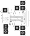
- the receiver 3 includes a mode separator 31 (mode separator) optically coupled to the optical transmission line 2 and a receiver main body 32 optically coupled to the mode separator 31.
- the mode separator 31 includes, for example, a main core 33, a separation core 34, and a clad 40 that surrounds the cores 33 and 34.
- the main core 33 is formed linearly from the incident end 33a toward the emission end 33b. Since at least a part of the incident end 33a overlaps with the emission end 23b of the transmission path core 23 of the optical transmission path 2 in plan view, the main core 33 receives light from the emission end 23b of the transmission path core 23.
- the main core 33 is disposed so as to be optically coupled to the transmission line core 23.
- the separation core 34 has an upstream portion 35, a coupling portion 36, a downstream portion 37, and an extending portion 38 in this order in the light transmission direction.
- the upstream portion 35 is a portion that gradually approaches the main core 33 as it goes downstream.
- the coupling portion 36 is a portion that is generally formed in parallel with the main core 33 at an interval that enables optical coupling.
- the downstream portion 37 is a portion that gradually separates from the main core 33 toward the downstream side.
- the extending portion 38 is a portion that extends from the downstream portion 37 and reaches the emission end 34b.
- the main core 33 is disposed so that the emitted light is incident on the first light receiving portion 42 because at least a part of the emission end 33b is in a position overlapping the first light receiving portion 42 of the receiving portion main body 32 in plan view.
- the main core 33 is disposed so as to be optically coupled to the first light receiving unit 42.
- the separation core 34 is at a position where at least a part of the emission end 34 b overlaps the second light receiving part 43 of the receiving part main body 32 in plan view, the emitted light is incident on the second light receiving part 43.
- the separation core 34 is disposed so as to be optically coupled to the second light receiving unit 43.
- the incident end 31a of the mode separator 31 is preferably fused and connected to the emission end 2b of the optical transmission line 2.
- the receiving unit main body 32 is, for example, a photodiode (PD: Photo Diode).
- PD photodiode
- Examples of the PD include a GaAs PIN type photodiode (PIN-PD) and an avalanche photodiode (APD).
- the receiving unit main body 32 includes a base part 41, and a first light receiving part 42 and a second light receiving part 43 provided on the base part 41.
- the first light receiving unit 42 and the second light receiving unit 43 are disposed on the base unit 41 at different positions in plan view.
- the first light L ⁇ b> 1 from the first light emitting unit 7 and the second light L ⁇ b> 2 from the second light emitting unit 8 are modulated independently.
- the first light L1 includes at least a fundamental mode (LP01 mode). Most of the first light L1 may be in the fundamental mode.
- the first light L1 enters the first core 28A from the incident end 28Aa, exits from the exit end 28Ab, enters the transmission path core 23 of the optical transmission path 2 from the incident end 23a, and transmits the transmission path of the optical transmission path 2.
- the data is transmitted toward the receiving unit 3 through the core 23.
- the second light L2 includes at least a higher-order mode (for example, LP11 mode and LP12 mode).
- a higher-order mode for example, LP11 mode and LP12 mode.
- the higher-order mode ratio is made larger than the higher-order mode ratio in the first light L1, for example, by the method described above.
- the second light L2 from the second light emitting unit 8 is incident on the second core 29A from the incident end 29Aa.
- the second core 29A and the third core 29B can be optically coupled, most of the fundamental mode of the second light L2 incident on the second core 29A remains in the second core 29A, and higher-order mode At least a part (for example, most of the higher order modes) transitions to the third core 29B.
- the second light L2 including the higher order mode transferred to the third core 29B is emitted from the emission end 29Bb, is incident on the transmission path core 23 of the optical transmission path 2, and passes through the transmission path core 23 of the optical transmission path 2. It is transmitted toward the receiver 3. Since the second core 29A is not optically coupled to the transmission line core 23 of the optical transmission line 2, the basic mode remaining in the second core 29A is not incident on the transmission line core 23 of the optical transmission line 2. . Even if the fundamental mode is incident on a portion other than the transmission path core 23 of the optical transmission path 2, it leaks in the course of transmission and disappears.
- the fundamental mode of the first light L1 and the higher-order mode of the second light L2 incident on the transmission path core 23 of the optical transmission path 2 are transmitted by the transmission path core 23.
- the light is incident on the main core 33 of the mode separator 31 of the receiver 3 from the output end 23b.
- the fundamental mode and the higher-order mode incident on the main core 33 at least a part of the fundamental mode (for example, most of the fundamental mode) transitions to the coupling portion 36 of the separation core 34.
- the basic mode transitioned to the separation core 34 is incident on the second light receiving unit 43 of the receiving unit main body 32 through the downstream portion 37 and the extending portion 38.
- the higher-order mode remaining in the main core 33 is incident on the first light receiving unit 42 of the receiving unit main body 32 from the emission end 33b. In this way, the receiving unit 3 receives the basic mode and the higher order mode separately.
- the second core 29A and the third core 29B of the directional coupler 12 are optically coupled so that a part of the higher-order mode can transition. ing.
- the third core 29B is optically coupled to the transmission path core 23 of the optical transmission path 2
- the higher-order mode transitioned from the second core 29A to the third core 29B is the optical transmission path 2 To the transmission line core 23. Therefore, apart from the first light emitting unit 7 or the second light emitting unit 8, the basic mode of the first light L1 from the first light emitting unit 7 and the first mode without using components for obtaining a plurality of modes, etc.
- Mode multiplex communication is possible using the higher-order mode of the second light L2 modulated independently of the light L1. Therefore, the structure of the optical transmission device 4 and the optical communication system 10 capable of mode multiplexing communication can be simplified, and the size and the price can be reduced.
- the optical transmission device 4 since the second waveguide region 27 includes the second core 29A and the third core 29B capable of optical coupling, noise is reduced by reducing the fundamental mode in the second light L2. The communication quality can be improved.
- FIG. 10 is a configuration diagram of the optical transmission device 54 of the optical communication system 60 according to the second embodiment.
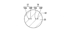
- FIG. 11 is a cross-sectional view of the directional coupler 62 used in the optical transmission device 54.
- symbol is attached
- the optical communication system 60 includes an optical transmission device 54 and a reception unit 3 (see FIGS. 1 and 9) optically coupled to the optical transmission device 54.
- the optical transmission device 54 includes a transmission unit 51 and an optical transmission path 2 that is optically coupled to the transmission unit 51.
- the transmission unit 51 includes a light source 11 and a directional coupler 62 optically coupled to the light source 11.
- the directional coupler 62 has a structure in which the first waveguide region 76 includes the first core 28A and the fourth core 28B formed at a distance allowing optical coupling with the first core 28A. It differs from the directional coupler 12 in the optical communication system 10 of 1st Embodiment shown in FIG.
- the first core 28 ⁇ / b> A and the fourth core 28 ⁇ / b> B are formed in parallel with each other at an interval that enables optical coupling.
- the first core 28A and the fourth core 28B are formed at an interval where at least a part of the higher-order mode is optically coupled so as to allow transition.
- Two or more of the first core 28A, the fourth core 28B, the second core 29A, and the third core 29B may have the same configuration (for example, material, outer diameter, etc.), or may have different configurations.
- the first core 28A may have the same configuration as the second core 29A or a different configuration.
- the fourth core 28B may have the same configuration as the third core 29B or may have a different configuration.
- the incident end 28Ba of the fourth core 28B is located away from the first light emitting unit 7 in plan view. That is, the fourth core 28 ⁇ / b> B is not optically coupled to the first light emitting unit 7.
- the emission end 28Bb of the fourth core 28B is located at a position away from the incident end 23a of the transmission path core 23 of the optical transmission path 2 in plan view. For this reason, the fourth core 28B is not optically coupled to the transmission path core 23 of the optical transmission path 2 at the emission end 28Bb.
- the first core 28A and the fourth core 28B can be optically coupled, most of the fundamental mode of the first light L1 incident on the first core 28A remains in the first core 28A, and higher-order mode At least a part (for example, most of the higher order modes) transitions to the fourth core 28B. Since the fourth core 28 ⁇ / b> B is not optically coupled to the transmission path core 23 of the optical transmission path 2, the higher-order mode transferred to the fourth core 28 ⁇ / b> B is not incident on the transmission path core 23.
- the optical transmission device 54 is a first mode in which the fundamental mode of the first light L1 from the first light emitting unit 7 is modulated independently of the first light L1. Mode multiplex communication using the higher-order mode of the second light L2 is possible. Therefore, the structures of the optical transmission device 54 and the optical communication system 60 can be simplified, and the size and the price can be reduced.
- the second waveguide region 27 includes the second core 29A and the third core 29B that can be optically coupled, the noise is reduced by reducing the fundamental mode in the second light L2, thereby reducing communication. Quality can be improved.
- the first waveguide region 76 of the directional coupler 62 has the fourth core 28B, it is possible to reduce higher-order modes in the first light L1. Therefore, it is possible to further reduce noise and realize high quality communication.
- FIG. 12 is a diagram illustrating the low cut filter 70.
- the low cut filter 70 is an electrical low cut filter that removes a part of the signal photoelectrically converted by the light receiving unit (for example, the first light receiving unit 42 in FIG. 9).
- the low-cut filter 70 is provided on the downstream side of the light receiving unit (for example, the first light receiving unit 42 in FIG. 9) where the higher-order mode is incident.
- the low cut filter 70 is, for example, a filter having a cutoff frequency of about 50 kHz, and a signal having a frequency of 50 kHz or less having an amplitude of 1/10 or less is preferable.
- the low cut filter 70 is provided.
- the signal from the first light emitting unit 7 is electrically cut, so that crosstalk is reduced and high quality communication is possible.
- the configuration in the embodiment is an example, and the addition, omission, replacement, and other modifications of the configuration can be made without departing from the spirit of the present invention.
- the second light emitting unit 8 receives the second light L ⁇ b> 2 only in the second core 29 ⁇ / b> A among the cores 29 ⁇ / b> A and 29 ⁇ / b> B of the second waveguide region 27.
- the configuration of the optical communication system is not limited to this.
- the second light emitting unit 8 is provided at a position where the second light L2 is incident only on the third core 29B of the cores 29A and 29B of the second waveguide region 27. Good.
- at least a part of the higher-order mode (for example, most of the higher-order mode) incident on the third core 29B remains in the third core 29B, and most of the fundamental mode of the second light L2 is the second core. Transition to 29A.
- the second light L2 including the higher-order mode remaining in the third core 29B is emitted from the emission end 29Bb, is incident on the transmission path core 23 of the optical transmission path 2, and is transmitted to the transmission path core of the optical transmission path 2. Then, the data is transmitted toward the receiving unit 3.
- the second core 29A is arranged not to be optically coupled to the second light emitting unit 8 and optically coupled to the transmission path core 23, and the third core 29B is optically coupled to the second light emitting unit 8 and transmitted. It may be arranged so as not to be optically coupled to the road core 23.
- the first light emitting unit 7 receives the first light L1 only in the first core 28A among the cores 28A and 28B of the first waveguide region 76.
- the second light emitting unit 8 is provided at a position where the second light L2 is incident only on the second core 29A out of the cores 29A and 29B of the second waveguide region 27.
- the system configuration is not limited to this.
- the optical communication system 60 for example, even if the first light emitting unit 7 is provided at a position where the first light L1 is incident only on the fourth core 28B of the cores 28A and 28B of the first waveguide region 76. Good. In this case, at least a part of the higher-order mode of the first light L1 incident on the fourth core 28B (for example, most of the higher-order mode) remains in the fourth core 28B, and the fundamental mode of the first light L1 At least a part (for example, most of the fundamental mode) transitions to the first core 28A.
- the first light L1 including the fundamental mode transitioned to the first core 28A is emitted from the emission end 28Ab, is incident on the transmission path core 23 of the optical transmission path 2, and is transmitted to the transmission path core 23 of the optical transmission path 2. And transmitted to the receiving unit 3.
- the second light emitting unit 8 may be provided at a position where the second light L2 is incident only on the third core 29B of the cores 29A and 29B of the second waveguide region 27.
- at least a part of the higher-order mode of the second light L2 incident on the third core 29B (for example, most of the higher-order mode) remains in the third core 29B
- the fundamental mode of the second light L2 At least a part (for example, most of the fundamental mode) transitions to the second core 29A.
- the second light L2 including the higher-order mode remaining in the third core 29B is emitted from the emission end 29Bb, is incident on the transmission path core 23 of the optical transmission path 2, and is transmitted to the transmission path core of the optical transmission path 2.
- the mode separator 31 shown in FIG. 9 is a waveguide type mode separator, but an optical fiber coupler type mode separator may be used instead.
- the VCSEL is exemplified as the light source 11.
- the light source 11 is not limited to this, and may be an edge-emitting laser that oscillates in multimode in the transverse mode.
- the mode separator 31 shown in FIG. 9 at least a part of the fundamental mode is separated from the main core 33.
- the fundamental mode and the higher order mode are separated from the main core. There may be.
- Receiver main part 33 ... Main core, 34 ... Separating core, 42 ... first light receiving part, 43 ... second light receiving part, 70 ... low cut filter, Da ... inner diameter of current confining layer of first light emitting part, Db ... current confining layer of second light emitting part Inner diameter of the opening, L1 ... first light, L2 ... second light
Landscapes
- Physics & Mathematics (AREA)
- Optics & Photonics (AREA)
- General Physics & Mathematics (AREA)
- Engineering & Computer Science (AREA)
- Computer Networks & Wireless Communication (AREA)
- Signal Processing (AREA)
- Electromagnetism (AREA)
- Condensed Matter Physics & Semiconductors (AREA)
- Microelectronics & Electronic Packaging (AREA)
- Optical Integrated Circuits (AREA)
- Optical Fibers, Optical Fiber Cores, And Optical Fiber Bundles (AREA)
- Semiconductor Lasers (AREA)
- Light Receiving Elements (AREA)
- Optical Communication System (AREA)
- Optical Couplings Of Light Guides (AREA)
Abstract
光源と、方向性結合器と、前記方向性結合器に光結合された伝送路コアを有する光伝送路とを備え、前記光源は、少なくとも基本モードを含む第1の光を発する第1発光部と、前記基本モードより次数が高い高次モードを含む第2の光を発する第2発光部と、を有し、前記方向性結合器は、少なくとも、前記第1発光部に光結合され、かつ前記伝送路コアに光結合されるように配置された第1コアを有する第1導波領域と、前記高次モードの少なくとも一部が遷移可能に互いに光結合するように、間隔をおいて形成された第2コアおよび第3コアを有する第2導波領域とを備え、前記第2コアと前記第3コアのうち一方は、前記第2発光部に光結合され、かつ前記伝送路コアに光結合されないように配置され、前記第2コアと前記第3コアのうち他方は、前記第2発光部に光結合されず、かつ前記伝送路コアに光結合されるように配置されている、光送信装置。
Description
本発明は、光送信装置および光通信システムに関する。
本願は、2016年10月21日に、日本に出願された特願2016-207302号に基づき優先権を主張し、その内容をここに援用する。
本願は、2016年10月21日に、日本に出願された特願2016-207302号に基づき優先権を主張し、その内容をここに援用する。
従来、光伝送モジュールの通信容量を増やすためには、波長多重、空間多重等の技術が用いられてきた。基幹通信ネットワークで使用されている1300~1650nmの長波長帯域では、波長可変レーザーを用いた波長分割多重方式(WDM)により、トランシーバー毎に波長を変え、その波長を多重化する方式が用いられてきた。
近年、WDMでは通信容量が不足しており、特許文献1および非特許文献1に記載されているように、モード多重を用いた研究が行われている。
特許文献1および非特許文献1には、光ファイバで横モードを多重化するため、モード合分波器を用いて基本モードと高次モードを励起し、光ファイバに入射する方法を用いる光送信装置が提案されている。また、特許文献2に記載のように、VCSELを用いた光送信装置では、シングルモード光をレンズなどの光学素子を使用して空間光学的に角度を付けて光ファイバに入射させ、その角度を調整することによってモードの多重化を行っている。
近年、WDMでは通信容量が不足しており、特許文献1および非特許文献1に記載されているように、モード多重を用いた研究が行われている。
特許文献1および非特許文献1には、光ファイバで横モードを多重化するため、モード合分波器を用いて基本モードと高次モードを励起し、光ファイバに入射する方法を用いる光送信装置が提案されている。また、特許文献2に記載のように、VCSELを用いた光送信装置では、シングルモード光をレンズなどの光学素子を使用して空間光学的に角度を付けて光ファイバに入射させ、その角度を調整することによってモードの多重化を行っている。
信学技報Vol.112、No.448、p.39~44
従来の光送信装置では、複数の横モードを得るために、光ファイバとレーザー光源との間に、光ファイバとレーザー光源それぞれと離間した比較的大型の部品を使用する必要があり、小型化、低価格化の阻害要因となっていた。
本発明の一態様は、構造が簡略であり、小型化および低価格化を図ることができる光送信装置および光通信システムを提供することを目的とする。
本発明の第1の態様に係る光送信装置は、光源と、方向性結合器と、前記方向性結合器に光結合された伝送路コアを有する光伝送路とを備え、前記光源は、少なくとも基本モードを含む第1の光を発する第1発光部と、前記基本モードより次数が高い高次モードを含む第2の光を発する第2発光部と、を有し、前記方向性結合器は、少なくとも、前記第1発光部に光結合され、かつ前記伝送路コアに光結合されるように配置された第1コアを有する第1導波領域と、前記高次モードの少なくとも一部が遷移可能に互いに光結合するように、間隔をおいて形成された第2コアおよび第3コアを有する第2導波領域とを備え、前記第2コアと前記第3コアのうち一方は、前記第2発光部に光結合され、かつ前記伝送路コアに光結合されないように配置され、前記第2コアと前記第3コアのうち他方は、前記第2発光部に光結合されず、かつ前記伝送路コアに光結合されるように配置されている。
ここで、前記第1導波領域が、前記高次モードの少なくとも一部が遷移可能に前記第1コアと光結合するように、前記第1コアと間隔をおいて形成された第4コアを有し、前記第4コアが、前記第1発光部に光結合されず、かつ前記伝送路コアに光結合されないように配置されていてもよい。
また、前記光源は面発光レーザーであり、前記第1発光部および前記第2発光部は、それぞれ多重量子井戸構造を有する活性層と、開口部を有する電流狭窄層とを少なくとも有し、前記第2発光部の前記電流狭窄層の前記開口部の内径は、前記第1発光部の前記電流狭窄層の前記開口部の内径より大きくてもよい。
また、前記光伝送路は、グレーデッドインデックス型光ファイバであってもよい。
また、前記方向性結合器は、前記第1コアと、前記第2コアと、前記第3コアと、を有するマルチコア光ファイバであってもよい。
ここで、前記第1導波領域が、前記高次モードの少なくとも一部が遷移可能に前記第1コアと光結合するように、前記第1コアと間隔をおいて形成された第4コアを有し、前記第4コアが、前記第1発光部に光結合されず、かつ前記伝送路コアに光結合されないように配置されていてもよい。
また、前記光源は面発光レーザーであり、前記第1発光部および前記第2発光部は、それぞれ多重量子井戸構造を有する活性層と、開口部を有する電流狭窄層とを少なくとも有し、前記第2発光部の前記電流狭窄層の前記開口部の内径は、前記第1発光部の前記電流狭窄層の前記開口部の内径より大きくてもよい。
また、前記光伝送路は、グレーデッドインデックス型光ファイバであってもよい。
また、前記方向性結合器は、前記第1コアと、前記第2コアと、前記第3コアと、を有するマルチコア光ファイバであってもよい。
本発明の第2の態様に係る光通信システムは、前記光送信装置と、前記光送信装置に光結合された受信部とを備え、前記受信部は、前記光伝送路に光結合されたモード分離部と、前記モード分離部に光結合された受信部本体とを備え、前記モード分離部は、前記光伝送路から入射された前記基本モードおよび前記高次モードが入射される主コアと、前記基本モードおよび前記高次モードのうち一方の少なくとも一部を前記主コアから分離する分離用コアとを有し、前記受信部本体は、前記主コアおよび前記分離用コアから出射された、前記基本モードおよび前記高次モードがそれぞれ入射される第1受光部および第2受光部を有する。
ここで、前記光通信システムにおいて、前記高次モードが入射される前記第1受光部または前記第2受光部の下流側に、前記第1受光部または前記第2受光部で光電変換された信号の一部を除去する電気的なローカットフィルタが設けられていてもよい。
ここで、前記光通信システムにおいて、前記高次モードが入射される前記第1受光部または前記第2受光部の下流側に、前記第1受光部または前記第2受光部で光電変換された信号の一部を除去する電気的なローカットフィルタが設けられていてもよい。
本発明の第3の態様に係る光送信装置は、光源と、方向性結合器と、前記方向性結合器に光結合された伝送路コアを有する光伝送路とを備え、前記光源は、少なくとも基本モードを含む第1の光を発する第1発光部と、前記基本モードより次数が高い高次モードを含む第2の光を発する第2発光部と、を有し、前記方向性結合器は、前記基本モードの少なくとも一部が遷移可能に互いに光結合するように、間隔をおいて形成された第1コアおよび第4コアを有する第1導波領域と、前記高次モードの少なくとも一部が遷移可能に互いに光結合するように、間隔をおいて形成された第2コアおよび第3コアを有する第2導波領域とを備え、前記第1コアは、前記第1発光部に光結合されず、かつ前記伝送路コアに光結合されるように配置され、前記第4コアは、前記第1発光部に光結合され、かつ前記伝送路コアに光結合されないように配置され、前記第2コアと前記第3コアのうち一方は、前記第2発光部に光結合され、かつ前記伝送路コアに光結合されないように配置され、前記第2コアと前記第3コアのうち他方は、前記第2発光部に光結合されず、かつ前記伝送路コアに光結合されるように配置されている。
上記態様によれば、第2導波領域の第2コアと第3コアとが、高次モードの一部が遷移可能に光結合している。また、第2コアと第3コアのうち一方が、光伝送路の伝送路コアに光結合されるように配置されているため、他方から遷移した高次モードが光伝送路コアに出射される。そのため、発光部とは別に、複数のモードを得るための部品等を用いずに、第1発光部からの第1の光の基本モードと、第1の光とは独立して変調された第2の光の高次モードとを用いたモード多重通信が可能である。よって、モード多重通信が可能な光送信装置の構造を簡略にし、小型化および低価格化を図ることができる。
以下、実施形態の光通信システムについて図面に基づいて説明する。なお、以下の説明で用いる図面は、特徴をわかりやすくするために、便宜上特徴となる部分を拡大して示している場合があり、各構成要素の寸法比率などが実際と同じであるとは限らない。また、本発明は以下の実施形態に限定されない。
<光送信装置および光通信システム(第1実施形態)>
図1は、第1実施形態の光通信システム10の構成図である。図2は、光通信システム10の光送信装置4の構成図である。図3は、光送信装置4に用いられる光源11の平面図である。図4は、光源11についての、後述する基板14の厚さ方向に沿う断面図である。図5は、光送信装置4に用いられる方向性結合器12の断面図である。
図1は、第1実施形態の光通信システム10の構成図である。図2は、光通信システム10の光送信装置4の構成図である。図3は、光送信装置4に用いられる光源11の平面図である。図4は、光源11についての、後述する基板14の厚さ方向に沿う断面図である。図5は、光送信装置4に用いられる方向性結合器12の断面図である。
図1に示すように、光通信システム10は、光送信装置4と、光送信装置4に光結合された受信部3とを備えている。光送信装置4は、送信部1と、送信部1に光結合された光伝送路2とを備えている。
(定義)
ここで、本実施形態において、光源(第1発光部もしくは第2発光部)と、導波領域コア(第1~第4コアのいずれか)とが光結合するとは、光源からの光が導波領域コアに入射することを言う。
例えば、以下の(i)~(iii)の場合に、光源と導波領域コアとが光結合しているという。(i)光源と導波領域コアとが互いに離間され、光源から出射された光が導波領域コアに入射する場合。(ii)光源と導波領域コアとが互いに離間され、光源と導波領域コアとが互いに光ファイバなどの中継用光伝送路を通じて接続され、光源から出射された光が中継用光伝送路を通して導波領域コアに入射する場合。(iii)光源と導波領域コアとが互いに接して設置され、光源から出射された光が導波領域コアに入射する場合。
また、導波領域コア(第1~第4コアのいずれか)と、光伝送路コアとが光結合するとは、例えば、導波領域コアから出射された光が光伝送路コアに入射することを言う。
また、2つのコア(第2コアと第3コア、もしくは、第1コアと第4コア)が、光の少なくとも一部が遷移可能に光結合するとは、例えば、2つのコアのうち一方のコアを伝搬する光の少なくとも一部が他方のコアに遷移し得ることを言う。
また、光伝送路コアと、モード分離器の主コアとが光結合するとは、例えば、光伝送路コアから出射された光が主コアに入射することを言う。
また、モード分離器の主コアもしくは分離用コアが、受光部(第1受光部または第2受光部)に光結合するとは、例えば、主コアもしくは分離用コアから出射された光が受光部に入射することを言う。
また、光通信システム10における光の伝送方向のうち、送信部1側を上流側といい、受信部3側を下流側という。
ここで、本実施形態において、光源(第1発光部もしくは第2発光部)と、導波領域コア(第1~第4コアのいずれか)とが光結合するとは、光源からの光が導波領域コアに入射することを言う。
例えば、以下の(i)~(iii)の場合に、光源と導波領域コアとが光結合しているという。(i)光源と導波領域コアとが互いに離間され、光源から出射された光が導波領域コアに入射する場合。(ii)光源と導波領域コアとが互いに離間され、光源と導波領域コアとが互いに光ファイバなどの中継用光伝送路を通じて接続され、光源から出射された光が中継用光伝送路を通して導波領域コアに入射する場合。(iii)光源と導波領域コアとが互いに接して設置され、光源から出射された光が導波領域コアに入射する場合。
また、導波領域コア(第1~第4コアのいずれか)と、光伝送路コアとが光結合するとは、例えば、導波領域コアから出射された光が光伝送路コアに入射することを言う。
また、2つのコア(第2コアと第3コア、もしくは、第1コアと第4コア)が、光の少なくとも一部が遷移可能に光結合するとは、例えば、2つのコアのうち一方のコアを伝搬する光の少なくとも一部が他方のコアに遷移し得ることを言う。
また、光伝送路コアと、モード分離器の主コアとが光結合するとは、例えば、光伝送路コアから出射された光が主コアに入射することを言う。
また、モード分離器の主コアもしくは分離用コアが、受光部(第1受光部または第2受光部)に光結合するとは、例えば、主コアもしくは分離用コアから出射された光が受光部に入射することを言う。
また、光通信システム10における光の伝送方向のうち、送信部1側を上流側といい、受信部3側を下流側という。
図2に示すように、送信部1は、光源11と、方向性結合器12とを備えている。
図3および図4に示すように、光源11は、例えば面発光レーザー(VCSEL:Vertical Cavity Surface Emitting Laser)である。VCSELの使用により、簡略な構造でありながら、基本モードと高次モードとを用いたモード多重通信を実現できる。
図3および図4に示すように、光源11は、例えば面発光レーザー(VCSEL:Vertical Cavity Surface Emitting Laser)である。VCSELの使用により、簡略な構造でありながら、基本モードと高次モードとを用いたモード多重通信を実現できる。
図4に示すように、光源11は、基台部6と、基台部6に設けられた第1発光部7および第2発光部8と、を備えている。
基台部6は、カソード電極13と、基板14と、第1ミラー層15とがこの順に積層されて構成されている。
図4に示すように、カソード電極13は、基板14の外面(図4の下面)に設けられている。
基板14としては、例えばn型のGaAs基板などが使用できる。
第1ミラー層15は、例えばn型の半導体層であり、低屈折率層と高屈折率層とを交互に積層した分布ブラッグ反射型(DBRミラー)である。
基台部6は、カソード電極13と、基板14と、第1ミラー層15とがこの順に積層されて構成されている。
図4に示すように、カソード電極13は、基板14の外面(図4の下面)に設けられている。
基板14としては、例えばn型のGaAs基板などが使用できる。
第1ミラー層15は、例えばn型の半導体層であり、低屈折率層と高屈折率層とを交互に積層した分布ブラッグ反射型(DBRミラー)である。
第1発光部7および第2発光部8は、基台部6上に、平面視において互いに異なる位置に配置されている。なお、平面視とは基板14の厚さ方向から見ることをいう。
第1発光部7は、活性層16Aと、電流狭窄層17Aと、第2ミラー層18Aと、パシベーション層19Aと、アノード電極20Aとが基台部6からこの順に積層されて構成されている。第2発光部8は、活性層16Bと、電流狭窄層17Bと、第2ミラー層18Bと、パシベーション層19Bと、アノード電極20Bとが基台部6からこの順に積層されて構成されている。
第1発光部7は、活性層16Aと、電流狭窄層17Aと、第2ミラー層18Aと、パシベーション層19Aと、アノード電極20Aとが基台部6からこの順に積層されて構成されている。第2発光部8は、活性層16Bと、電流狭窄層17Bと、第2ミラー層18Bと、パシベーション層19Bと、アノード電極20Bとが基台部6からこの順に積層されて構成されている。
活性層16A,16Bは、例えば量子井戸層と障壁層とからなる量子井戸構造を複数備えた多重量子井戸構造を有する。
電流狭窄層17A,17Bは、例えばAlAs層を酸化して得られ、それぞれ開口部17Aa,17Baを有する。
第2ミラー層18A,18Bは、例えばp型の半導体層であり、低屈折率層と高屈折率層とを交互に積層した分布ブラッグ反射型(DBRミラー)である。
電流狭窄層17A,17Bは、例えばAlAs層を酸化して得られ、それぞれ開口部17Aa,17Baを有する。
第2ミラー層18A,18Bは、例えばp型の半導体層であり、低屈折率層と高屈折率層とを交互に積層した分布ブラッグ反射型(DBRミラー)である。
パシベーション層19Aは、例えば第2ミラー層18Aを包囲して形成されている。パシベーション層19Aは、平面視において少なくとも電流狭窄層17Aの開口部17Aaを囲む開口部19Aaを有する。なお、平面視とは基板14の厚さ方向から見ることをいう。
アノード電極20Aは、パシベーション層19Aおよび第2ミラー層18Aを囲んで設けられている。アノード電極20Aは、平面視において電流狭窄層17Aの開口部17Aaを囲む開口部20Aaを有する。
第1発光部7では、開口部20Aaを通って第1の光L1(図2参照)が外部に出射される。
アノード電極20Aは、パシベーション層19Aおよび第2ミラー層18Aを囲んで設けられている。アノード電極20Aは、平面視において電流狭窄層17Aの開口部17Aaを囲む開口部20Aaを有する。
第1発光部7では、開口部20Aaを通って第1の光L1(図2参照)が外部に出射される。
パシベーション層19Bは、例えば第2ミラー層18Bを包囲して形成されている。パシベーション層19Bは、平面視において少なくとも電流狭窄層17Bの開口部17Baを囲む開口部19Baを有する。
アノード電極20Bは、パシベーション層19Bおよび第2ミラー層18Bを囲んで設けられている。アノード電極20Bは、平面視において電流狭窄層17Bの開口部17Baを囲む開口部20Baを有する。
第2発光部8では、開口部20Baを通って第2の光L2(図2参照)が外部に出射される。
図3に示す一対のアノード電極端子21は、図4に示すアノード電極20A,20Bにそれぞれ接続されている。図3に示す一対のカソード電極端子22はそれぞれ、図4に示すカソード電極13に接続されている。
アノード電極20Bは、パシベーション層19Bおよび第2ミラー層18Bを囲んで設けられている。アノード電極20Bは、平面視において電流狭窄層17Bの開口部17Baを囲む開口部20Baを有する。
第2発光部8では、開口部20Baを通って第2の光L2(図2参照)が外部に出射される。
図3に示す一対のアノード電極端子21は、図4に示すアノード電極20A,20Bにそれぞれ接続されている。図3に示す一対のカソード電極端子22はそれぞれ、図4に示すカソード電極13に接続されている。
図6は、第2発光部8が出射する光のスペクトルの例を示す図である。図6に示すように、この光は、横モードの次数が異なる複数のモードを含む。前記光は、最も波長が長い基本モード(LP01モード)と、基本モードより次数が高い高次モード(LP11モードおよびLP12モード)とを含む。ここで、一般的に、横モードの次数を表現する場合、LPモード(linearly polarized propagation mode)を用いている。以降、横モードの次数を表現する場合、LPモードを用いることがある。LP11モードのピークの波長はLP01モードのピークの波長よりも短い。LP12モードのピークの波長はLP11モードのピークの波長よりも短い。
図4に示す、電流狭窄層17A,17Bの開口部17Aa,17Baの内径Da,Dbは、発光部7,8からの出射光に含まれる基本モードと高次モードとの比率に影響する。例えば、開口部17Aa,17Baの内径Da,Dbが小さいほど、全体に占める基本モードの比率が大きくなる傾向がある。また、開口部17Aa,17Baの内径Da,Dbが大きいほど、全体に占める高次モードの比率が大きくなる傾向がある。そのため、開口部17Aa,17Baの内径Da,Dbの選択により基本モードと高次モードとの比率を調整することができる。
光源11では、第1発光部7の開口部17Aaの内径Daと、第2発光部8の開口部17Baの内径Dbとが異なることによって、基本モードと高次モードとの比率が異なる第1の光L1と第2の光L2が得られる。例えば、第2発光部8の開口部17Baの内径Dbを、第1発光部7の開口部17Aaの内径Daより大きく設定することによって、第2の光L2における高次モード(例えばLP11モードおよびLP12モード)の比率を、第1の光L1における高次モードの比率より大きくすることができる。
第1発光部7の開口部17Aaの内径Daは、例えば5.5~6.5μmである。第2発光部8の開口部17Baの内径Dbは、例えば8~10μmである。
第1発光部7の開口部17Aaの内径Daは、例えば5.5~6.5μmである。第2発光部8の開口部17Baの内径Dbは、例えば8~10μmである。
光源11におけるバイアス電流は、出射光の基本モードと高次モードとの比率に影響する。例えば、閥値Ithから3mA程度の低電流値では基本モードの比率が大きくなり、9mA程度の高電流値では、高次モードの比率が大きくなる。すなわち、光源11におけるバイアス電流の電流値を上げていくと高次モードの比率が大きくなる。そのため、バイアス電流により基本モードと高次モードとの比率を調整することができる。例えば、第1発光部7および第2発光部8におけるバイアス電流を適切に設定すれば、第2の光L2における高次モードの比率を、第1の光L1における高次モードの比率より大きくすることができる。
図2に示すように、第1発光部7は、少なくとも基本モード(LP01モード)を含む第1の光L1を発する。第1の光L1は、大部分が基本モードであることが好ましい。第1の光L1の大部分が基本モードであると、光伝送路2での光伝送時におけるノイズを低減できる。
第2発光部8は、少なくとも高次モードを含む第2の光L2を発する。第2の光L2は、基本モードと高次モードとを含んでいてもよい。高次モードは、例えばLP11モードおよびLP12モードである。第2の光L2における高次モードの比率が大きいと、光伝送路2での光伝送時におけるノイズを低減できる。
第2発光部8は、少なくとも高次モードを含む第2の光L2を発する。第2の光L2は、基本モードと高次モードとを含んでいてもよい。高次モードは、例えばLP11モードおよびLP12モードである。第2の光L2における高次モードの比率が大きいと、光伝送路2での光伝送時におけるノイズを低減できる。
図2および図5に示すように、方向性結合器12は、第1導波領域26と、第2導波領域27と、クラッド25と、を有する。クラッド25は、第1導波領域26および第2導波領域27を囲んでいる。方向性結合器12は、光源11から光伝送路2に向けて延びている。
第1導波領域26は、第1コア28Aを有する。第1コア28Aは、方向性結合器12が延びる長手方向に沿って延在している。
第2導波領域27は、第2コア29Aと第3コア29Bとを有する。第2コア29Aおよび第3コア29Bは、方向性結合器12の長手方向に沿って延在している。第2コア29Aと第3コア29Bとは、互いに、光結合が可能となる間隔をおいて並列して形成されている。第2コア29Aと第3コア29Bとは、高次モードの少なくとも一部が遷移可能に光結合する間隔をおいて形成されている。
方向性結合器12としては、コア28A,29A,29Bと、コア28A,29A,29Bを囲むクラッド25とを有するマルチコア光ファイバを使用できる。マルチコア光ファイバは、ステップインデックス(SI)型であることが好ましい。
第1コア28A、第2コア29Aおよび第3コア29Bのうち2以上は、互いに同じ構成(例えば材質、外径等)であってもよいし、互いに異なる構成であってもよい。例えば、第2コア29Aと第1コア28Aとは同じ構成であってよいし、異なる構成であってもよい。
第1導波領域26は、第1コア28Aを有する。第1コア28Aは、方向性結合器12が延びる長手方向に沿って延在している。
第2導波領域27は、第2コア29Aと第3コア29Bとを有する。第2コア29Aおよび第3コア29Bは、方向性結合器12の長手方向に沿って延在している。第2コア29Aと第3コア29Bとは、互いに、光結合が可能となる間隔をおいて並列して形成されている。第2コア29Aと第3コア29Bとは、高次モードの少なくとも一部が遷移可能に光結合する間隔をおいて形成されている。
方向性結合器12としては、コア28A,29A,29Bと、コア28A,29A,29Bを囲むクラッド25とを有するマルチコア光ファイバを使用できる。マルチコア光ファイバは、ステップインデックス(SI)型であることが好ましい。
第1コア28A、第2コア29Aおよび第3コア29Bのうち2以上は、互いに同じ構成(例えば材質、外径等)であってもよいし、互いに異なる構成であってもよい。例えば、第2コア29Aと第1コア28Aとは同じ構成であってよいし、異なる構成であってもよい。
図7は、一対のコア(第2コア29Aおよび第3コア29B)を有する方向性結合器12において、第2コア29Aと第3コア29Bの中心間距離d(横軸)と結合長(縦軸)との関係の例を示す図である。
図8は、上記中心間距離d(横軸)と、第2コア29AにおけるLP01モードのパワー残量(縦軸)と、の関係の例を示す図である。なお、第2コア29Aおよび第3コア29Bは、直径8μm、比屈折率差0.3%とした。また、入射させる光の波長は850nmとした。
図8は、上記中心間距離d(横軸)と、第2コア29AにおけるLP01モードのパワー残量(縦軸)と、の関係の例を示す図である。なお、第2コア29Aおよび第3コア29Bは、直径8μm、比屈折率差0.3%とした。また、入射させる光の波長は850nmとした。
図7および図8に示すように、コアの結合長は中心間距離dに応じて変化する。中心間距離dが14μmの場合には、コアの長さを100mm以上とすると、95%以上のLP01モードを第2コア29Aに残しつつ、LP11モードの大部分を第2コア29Aから第3コア29Bに遷移させることができる。
よって、図2および図5に示す方向性結合器12では、例えば第2コア29Aと第3コア29Bとの中心間距離dを13~15μm、長さ100mm以上(例えば100~150mm)とすることが好ましい。
よって、図2および図5に示す方向性結合器12では、例えば第2コア29Aと第3コア29Bとの中心間距離dを13~15μm、長さ100mm以上(例えば100~150mm)とすることが好ましい。
第1導波領域26の第1コア28Aは、入射端28Aaの少なくとも一部が平面視において光源11の第1発光部7に重なる位置にあるため、第1発光部7からの第1の光L1が入射端28Aaから入射されるように配置されている。すなわち、第1コア28Aは、第1発光部7に光結合されるように配置されている。
第1コア28Aの出射端28Abは、少なくとも一部が平面視において光伝送路2の伝送路コア23の入射端23aに重なる位置にあるため、第1コア28Aは、出射端28Abが光伝送路2の伝送路コア23に光結合されるように配置されている。
第1コア28Aの出射端28Abは、少なくとも一部が平面視において光伝送路2の伝送路コア23の入射端23aに重なる位置にあるため、第1コア28Aは、出射端28Abが光伝送路2の伝送路コア23に光結合されるように配置されている。
第2導波領域27の第2コア29Aは、入射端29Aaの少なくとも一部が平面視において光源11の第2発光部8に重なる位置にあるため、第2発光部8からの第2の光L2が入射端29Aaから入射されるように配置されている。すなわち、第2コア29Aは、第2発光部8に光結合されるように配置されている。
第2コア29Aの出射端29Abは、平面視において光伝送路2の伝送路コア23の入射端23aから離れた位置にある。そのため、第2コア29Aは、出射端29Abにおいて光伝送路2の伝送路コア23に光結合されていない。なお、第2コア29Aは、大部分の光が光伝送路2の伝送路コア23に出射されないように配置されていてもよい。
第2コア29Aの出射端29Abは、平面視において光伝送路2の伝送路コア23の入射端23aから離れた位置にある。そのため、第2コア29Aは、出射端29Abにおいて光伝送路2の伝送路コア23に光結合されていない。なお、第2コア29Aは、大部分の光が光伝送路2の伝送路コア23に出射されないように配置されていてもよい。
第2導波領域27の第3コア29Bの入射端29Baは、平面視において第2発光部8から離れた位置にある。そのため、第3コア29Bは、第2発光部8に光結合されていない。
第3コア29Bの出射端29Bbは、少なくとも一部が平面視において光伝送路2の伝送路コア23の入射端23aに重なる位置にある。そのため、第3コア29Bは、光が出射端29Bbから光伝送路2の伝送路コア23に出射されるように配置されている。すなわち、第3コア29Bは、光伝送路2の伝送路コア23に光結合されている。
第3コア29Bの出射端29Bbは、少なくとも一部が平面視において光伝送路2の伝送路コア23の入射端23aに重なる位置にある。そのため、第3コア29Bは、光が出射端29Bbから光伝送路2の伝送路コア23に出射されるように配置されている。すなわち、第3コア29Bは、光伝送路2の伝送路コア23に光結合されている。
光伝送路2は、例えば、伝送路コア23と、伝送路コア23を囲むクラッド24とを有する光ファイバである。光伝送路2は、グレーデッドインデックス(GI)型光ファイバであることが好ましい。GI型光ファイバを使用することによって、安定した信号が得られる。
光伝送路2の入射端2aは、方向性結合器12の出射端12bと融着接続されていることが好ましい。
光伝送路2の入射端2aは、方向性結合器12の出射端12bと融着接続されていることが好ましい。
図9に示すように、受信部3は、光伝送路2に光結合されたモード分離器31(モード分離部)と、モード分離器31に光結合された受信部本体32とを備えている。
モード分離器31は、例えば、主コア33と、分離用コア34と、コア33,34を囲むクラッド40とを有する。
主コア33は、入射端33aから出射端33bに向けて直線状に形成されている。入射端33aは少なくとも一部が平面視において光伝送路2の伝送路コア23の出射端23bに重なる位置にあるため、主コア33は、光が伝送路コア23の出射端23bから入射されるように配置されている。すなわち、主コア33は、伝送路コア23に光結合するように配置されている。
モード分離器31は、例えば、主コア33と、分離用コア34と、コア33,34を囲むクラッド40とを有する。
主コア33は、入射端33aから出射端33bに向けて直線状に形成されている。入射端33aは少なくとも一部が平面視において光伝送路2の伝送路コア23の出射端23bに重なる位置にあるため、主コア33は、光が伝送路コア23の出射端23bから入射されるように配置されている。すなわち、主コア33は、伝送路コア23に光結合するように配置されている。
分離用コア34は、光の伝送方向に、上流側部分35と、結合部分36と、下流側部分37と、延出部分38をこの順に有する。
上流側部分35は、下流側に向かうに従って、主コア33に徐々に近づく部分である。結合部分36は、光結合が可能となる間隔をおいて、概略、主コア33に並行して形成された部分である。下流側部分37は、下流側に向かうに従って、主コア33から徐々に離間する部分である。延出部分38は、下流側部分37から延出し、出射端34bに達する部分である。
上流側部分35は、下流側に向かうに従って、主コア33に徐々に近づく部分である。結合部分36は、光結合が可能となる間隔をおいて、概略、主コア33に並行して形成された部分である。下流側部分37は、下流側に向かうに従って、主コア33から徐々に離間する部分である。延出部分38は、下流側部分37から延出し、出射端34bに達する部分である。
主コア33は、出射端33bの少なくとも一部が平面視において受信部本体32の第1受光部42に重なる位置にあるため、出射された光が第1受光部42に入射されるように配置されている。すなわち、主コア33は、第1受光部42に光結合されるように配置されている。
分離用コア34は、出射端34bの少なくとも一部が平面視において受信部本体32の第2受光部43に重なる位置にあるため、出射された光が第2受光部43に入射されるように配置されている。すなわち、分離用コア34は、第2受光部43に光結合されるように配置されている。
モード分離器31の入射端31aは、光伝送路2の出射端2bと融着接続されていることが好ましい。
分離用コア34は、出射端34bの少なくとも一部が平面視において受信部本体32の第2受光部43に重なる位置にあるため、出射された光が第2受光部43に入射されるように配置されている。すなわち、分離用コア34は、第2受光部43に光結合されるように配置されている。
モード分離器31の入射端31aは、光伝送路2の出射端2bと融着接続されていることが好ましい。
受信部本体32は、例えばフォトダイオード(PD:Photo Diode)である。PDとしては、GaAsのPIN型フォトダイオード(PIN-PD)、アバランシェフォトダイオード(APD)などが挙げられる。
受信部本体32は、基台部41と、基台部41に設けられた第1受光部42および第2受光部43と、を備えている。
第1受光部42および第2受光部43は、基台部41上に、平面視において互いに異なる位置に配置されている。
受信部本体32は、基台部41と、基台部41に設けられた第1受光部42および第2受光部43と、を備えている。
第1受光部42および第2受光部43は、基台部41上に、平面視において互いに異なる位置に配置されている。
次に、光通信システム10を用いた通信方法の一例を説明する。
図2に示すように、光源11においては、第1発光部7からの第1の光L1と、第2発光部8からの第2の光L2とは、独立して変調される。
第1の光L1は、少なくとも基本モード(LP01モード)を含む。第1の光L1は、大部分が基本モードであってよい。
第1の光L1は、入射端28Aaから第1コア28Aに入射されて出射端28Abから出射され、入射端23aから光伝送路2の伝送路コア23に入射され、光伝送路2の伝送路コア23を通じて、受信部3に向かって伝送される。
図2に示すように、光源11においては、第1発光部7からの第1の光L1と、第2発光部8からの第2の光L2とは、独立して変調される。
第1の光L1は、少なくとも基本モード(LP01モード)を含む。第1の光L1は、大部分が基本モードであってよい。
第1の光L1は、入射端28Aaから第1コア28Aに入射されて出射端28Abから出射され、入射端23aから光伝送路2の伝送路コア23に入射され、光伝送路2の伝送路コア23を通じて、受信部3に向かって伝送される。
第2の光L2は、少なくとも高次モード(例えばLP11モードおよびLP12モード)を含む。第2の光L2は、例えば上述の手法により、高次モードの比率が第1の光L1における高次モードの比率より大きくされていることが好ましい。
第2発光部8からの第2の光L2は、入射端29Aaから第2コア29Aに入射される。
第2発光部8からの第2の光L2は、入射端29Aaから第2コア29Aに入射される。
第2コア29Aと第3コア29Bとは光結合が可能であるため、第2コア29Aに入射された第2の光L2の基本モードの大部分は第2コア29Aに残り、高次モードの少なくとも一部(例えば高次モードの大部分)は第3コア29Bに遷移する。
第3コア29Bに移った高次モードを含む第2の光L2は、出射端29Bbから出射され、光伝送路2の伝送路コア23に入射され、光伝送路2の伝送路コア23を通じて、受信部3に向かって伝送される。
なお、第2コア29Aは、光伝送路2の伝送路コア23には光結合されていないため、第2コア29Aに残った基本モードは、光伝送路2の伝送路コア23には入射されない。この基本モードは、光伝送路2の伝送路コア23以外の部分に入射されたとしても伝送の過程で漏洩するため消失する。
第3コア29Bに移った高次モードを含む第2の光L2は、出射端29Bbから出射され、光伝送路2の伝送路コア23に入射され、光伝送路2の伝送路コア23を通じて、受信部3に向かって伝送される。
なお、第2コア29Aは、光伝送路2の伝送路コア23には光結合されていないため、第2コア29Aに残った基本モードは、光伝送路2の伝送路コア23には入射されない。この基本モードは、光伝送路2の伝送路コア23以外の部分に入射されたとしても伝送の過程で漏洩するため消失する。
図9に示すように、光伝送路2の伝送路コア23に入射された、第1の光L1の基本モードと第2の光L2の高次モードとは、伝送路コア23にて伝送され、出射端23bから受信部3のモード分離器31の主コア33に入射される。
主コア33に入射された基本モードおよび高次モードのうち、基本モードの少なくとも一部(例えば基本モードの大部分)は、分離用コア34の結合部分36に遷移する。分離用コア34に遷移した基本モードは、下流側部分37および延出部分38を経て、受信部本体32の第2受光部43に入射される。
主コア33に残った高次モードは、出射端33bから受信部本体32の第1受光部42に入射される。
このようにして、受信部3では、基本モードと高次モードとが分離されて受信される。
主コア33に残った高次モードは、出射端33bから受信部本体32の第1受光部42に入射される。
このようにして、受信部3では、基本モードと高次モードとが分離されて受信される。
以上説明したように、図1および図2に示す光送信装置4では、方向性結合器12の第2コア29Aと第3コア29Bとが、高次モードの一部が遷移可能に光結合している。また、第3コア29Bが、光伝送路2の伝送路コア23に光結合されて配置されているため、第2コア29Aから第3コア29Bへと遷移した高次モードは、光伝送路2の伝送路コア23に出射される。そのため、第1発光部7または第2発光部8とは別に、複数のモードを得るための部品等を用いずに、第1発光部7からの第1の光L1の基本モードと、第1の光L1とは独立して変調された第2の光L2の高次モードとを用いたモード多重通信が可能である。よって、モード多重通信が可能な光送信装置4および光通信システム10の構造を簡略にし、小型化および低価格化を図ることができる。
また、光送信装置4は、第2導波領域27が、光結合が可能な第2コア29Aと第3コア29Bとを有するため、第2の光L2における基本モードを低減することによって、ノイズを低くし、通信の品質を高めることができる。
また、光送信装置4は、第2導波領域27が、光結合が可能な第2コア29Aと第3コア29Bとを有するため、第2の光L2における基本モードを低減することによって、ノイズを低くし、通信の品質を高めることができる。
<光送信装置および光通信システム(第2実施形態)>
図10は、第2実施形態の光通信システム60の光送信装置54の構成図である。図11は、光送信装置54に用いられる方向性結合器62の断面図である。なお、第1実施形態と共通の構成については同じ符号を付してその説明を省略する。
図10は、第2実施形態の光通信システム60の光送信装置54の構成図である。図11は、光送信装置54に用いられる方向性結合器62の断面図である。なお、第1実施形態と共通の構成については同じ符号を付してその説明を省略する。
図10に示すように、光通信システム60は、光送信装置54と、光送信装置54に光結合された受信部3(図1および図9参照)とを備えている。光送信装置54は、送信部51と、送信部51に光結合された光伝送路2とを備えている。
送信部51は、光源11と、光源11に光結合された方向性結合器62とを備えている。
送信部51は、光源11と、光源11に光結合された方向性結合器62とを備えている。
方向性結合器62は、第1導波領域76が、第1コア28Aと、第1コア28Aと光結合可能となる間隔をおいて形成された第4コア28Bとを有する点で、図2に示す第1実施形態の光通信システム10における方向性結合器12と異なる。
第1コア28Aと第4コア28Bとは、互いに、光結合が可能となる間隔をおいて並列して形成されている。第1コア28Aと第4コア28Bとは、高次モードの少なくとも一部が遷移可能に光結合する間隔をおいて形成されている。
第1コア28A、第4コア28B、第2コア29Aおよび第3コア29Bのうち2以上は、互いに同じ構成(例えば材質、外径等)であってもよいし、互いに異なる構成であってもよい。例えば、第1コア28Aは第2コア29Aと同じ構成であってもよいし、異なる構成であってもよい。第4コア28Bは第3コア29Bと同じ構成であってもよいし、異なる構成であってもよい。
第1コア28A、第4コア28B、第2コア29Aおよび第3コア29Bのうち2以上は、互いに同じ構成(例えば材質、外径等)であってもよいし、互いに異なる構成であってもよい。例えば、第1コア28Aは第2コア29Aと同じ構成であってもよいし、異なる構成であってもよい。第4コア28Bは第3コア29Bと同じ構成であってもよいし、異なる構成であってもよい。
第4コア28Bの入射端28Baは、平面視において第1発光部7を外れた位置にある。つまり、第4コア28Bは、第1発光部7に光結合されていない。
第4コア28Bの出射端28Bbは、平面視において光伝送路2の伝送路コア23の入射端23aを外れた位置にある。そのため、第4コア28Bは、出射端28Bbにおいて光伝送路2の伝送路コア23に光結合されていない。
第4コア28Bの出射端28Bbは、平面視において光伝送路2の伝送路コア23の入射端23aを外れた位置にある。そのため、第4コア28Bは、出射端28Bbにおいて光伝送路2の伝送路コア23に光結合されていない。
第1コア28Aと第4コア28Bとは光結合が可能であるため、第1コア28Aに入射された第1の光L1の基本モードの大部分は第1コア28Aに残り、高次モードの少なくとも一部(例えば高次モードの大部分)は第4コア28Bに遷移する。
第4コア28Bは、光伝送路2の伝送路コア23には光結合されていないため、第4コア28Bに移った高次モードは、伝送路コア23には入射されない。
第4コア28Bは、光伝送路2の伝送路コア23には光結合されていないため、第4コア28Bに移った高次モードは、伝送路コア23には入射されない。
光送信装置54は、第1実施形態の光送信装置4と同様に、第1発光部7からの第1の光L1の基本モードと、第1の光L1とは独立して変調された第2の光L2の高次モードとを用いたモード多重通信が可能である。よって、光送信装置54および光通信システム60の構造を簡略にし、小型化および低価格化を図ることができる。
また、第2導波領域27は、光結合が可能な第2コア29Aと第3コア29Bとを有するため、第2の光L2における基本モードを低減することによって、ノイズを低くし、通信の品質を高めることができる。
さらに、光送信装置54では、方向性結合器62の第1導波領域76が第4コア28Bを有するため、第1の光L1における高次モードを低減できる。よって、一層の低ノイズ化を図り、通信の高品質化を実現できる。
また、第2導波領域27は、光結合が可能な第2コア29Aと第3コア29Bとを有するため、第2の光L2における基本モードを低減することによって、ノイズを低くし、通信の品質を高めることができる。
さらに、光送信装置54では、方向性結合器62の第1導波領域76が第4コア28Bを有するため、第1の光L1における高次モードを低減できる。よって、一層の低ノイズ化を図り、通信の高品質化を実現できる。
図12は、ローカットフィルタ70を示す図である。
ローカットフィルタ70は、受光部(例えば図9の第1受光部42)で光電変換された信号の一部を除去する電気的なローカットフィルタである。ローカットフィルタ70は、高次モードが入射される受光部(例えば図9の第1受光部42)の下流側に設けられる。ローカットフィルタ70は、例えばカットオフ周波数50kHz程度のフィルタであり、周波数50kHz以下の信号が1/10以下の振幅となるものが好ましい。
例えば、第1発光部7の信号が低速(例えば10kbps以下)の制御信号であり、第2発光部8の信号が高速(例えば10Gbps以上)のデータ信号である場合には、ローカットフィルタ70を設けることによって、主として第1発光部7からの信号が電気的にカットされるため、クロストークが低減され、高品質な通信が可能となる。
ローカットフィルタ70は、受光部(例えば図9の第1受光部42)で光電変換された信号の一部を除去する電気的なローカットフィルタである。ローカットフィルタ70は、高次モードが入射される受光部(例えば図9の第1受光部42)の下流側に設けられる。ローカットフィルタ70は、例えばカットオフ周波数50kHz程度のフィルタであり、周波数50kHz以下の信号が1/10以下の振幅となるものが好ましい。
例えば、第1発光部7の信号が低速(例えば10kbps以下)の制御信号であり、第2発光部8の信号が高速(例えば10Gbps以上)のデータ信号である場合には、ローカットフィルタ70を設けることによって、主として第1発光部7からの信号が電気的にカットされるため、クロストークが低減され、高品質な通信が可能となる。
以上、本発明の実施形態を説明したが、実施形態における構成は一例であり、本発明の趣旨から逸脱しない範囲内で、構成の付加、省略、置換、およびその他の変更が可能である。
例えば、図1に示す第1実施形態の光通信システム10では、第2発光部8は、第2導波領域27のコア29A,29Bのうち第2コア29Aにのみ第2の光L2が入射される位置に設けられているが、光通信システムの構成はこれに限定されない。
光通信システム10は、例えば、第2発光部8が、第2導波領域27のコア29A,29Bのうち第3コア29Bにのみ第2の光L2が入射される位置に設けられていてもよい。この場合、第3コア29Bに入射された高次モードの少なくとも一部(例えば高次モードの大部分)は第3コア29Bに残り、第2の光L2の基本モードの大部分は第2コア29Aに遷移する。ここで、第3コア29Bに残った高次モードを含む第2の光L2は、出射端29Bbから出射され、光伝送路2の伝送路コア23に入射され、光伝送路2の伝送路コア23を通じて、受信部3に向かって伝送される。また、第2コア29Aが第2発光部8に光結合されず、かつ伝送路コア23に光結合されるように配置され、第3コア29Bが第2発光部8に光結合され、かつ伝送路コア23に光結合されないように配置されてもよい。
例えば、図1に示す第1実施形態の光通信システム10では、第2発光部8は、第2導波領域27のコア29A,29Bのうち第2コア29Aにのみ第2の光L2が入射される位置に設けられているが、光通信システムの構成はこれに限定されない。
光通信システム10は、例えば、第2発光部8が、第2導波領域27のコア29A,29Bのうち第3コア29Bにのみ第2の光L2が入射される位置に設けられていてもよい。この場合、第3コア29Bに入射された高次モードの少なくとも一部(例えば高次モードの大部分)は第3コア29Bに残り、第2の光L2の基本モードの大部分は第2コア29Aに遷移する。ここで、第3コア29Bに残った高次モードを含む第2の光L2は、出射端29Bbから出射され、光伝送路2の伝送路コア23に入射され、光伝送路2の伝送路コア23を通じて、受信部3に向かって伝送される。また、第2コア29Aが第2発光部8に光結合されず、かつ伝送路コア23に光結合されるように配置され、第3コア29Bが第2発光部8に光結合され、かつ伝送路コア23に光結合されないように配置されてもよい。
図10に示す第2実施形態の光通信システム60では、第1発光部7は、第1導波領域76のコア28A,28Bのうち第1コア28Aにのみ第1の光L1が入射される位置に設けられ、第2発光部8は、第2導波領域27のコア29A,29Bのうち第2コア29Aにのみ第2の光L2が入射される位置に設けられているが、光通信システムの構成はこれに限定されない。
光通信システム60は、例えば、第1発光部7が、第1導波領域76のコア28A,28Bのうち第4コア28Bにのみ第1の光L1が入射される位置に設けられていてもよい。この場合、第4コア28Bに入射された第1の光L1の高次モードの少なくとも一部(例えば高次モードの大部分)は第4コア28Bに残り、第1の光L1の基本モードの少なくとも一部(例えば基本モードの大部分)は第1コア28Aに遷移する。ここで、第1コア28Aに遷移した基本モードを含む第1の光L1は、出射端28Abから出射され、光伝送路2の伝送路コア23に入射され、光伝送路2の伝送路コア23を通じて、受信部3に向かって伝送される。
第2発光部8は、第2導波領域27のコア29A,29Bのうち第3コア29Bにのみ第2の光L2が入射される位置に設けられていてもよい。この場合、第3コア29Bに入射された第2の光L2の高次モードの少なくとも一部(例えば高次モードの大部分)は第3コア29Bに残り、第2の光L2の基本モードの少なくとも一部(例えば基本モードの大部分)は第2コア29Aに遷移する。ここで、第3コア29Bに残った高次モードを含む第2の光L2は、出射端29Bbから出射され、光伝送路2の伝送路コア23に入射され、光伝送路2の伝送路コア23を通じて、受信部3に向かって伝送される。
図9に示すモード分離器31は、導波路型のモード分離器であるが、これに代えて、光ファイバカプラ型のモード分離器を用いてもよい。
また、実施形態の光通信システムでは、光源11としてVCSELを例示したが、光源11はこれに限らず、横モードが多モード発振する端面発光レーザーなどでもよい。
図9に示すモード分離器31においては、基本モードの少なくとも一部が主コア33から分離されるが、モード分離器31において主コアから分離されるのは、基本モードおよび高次モードのいずれであってもよい。
図9に示すモード分離器31は、導波路型のモード分離器であるが、これに代えて、光ファイバカプラ型のモード分離器を用いてもよい。
また、実施形態の光通信システムでは、光源11としてVCSELを例示したが、光源11はこれに限らず、横モードが多モード発振する端面発光レーザーなどでもよい。
図9に示すモード分離器31においては、基本モードの少なくとも一部が主コア33から分離されるが、モード分離器31において主コアから分離されるのは、基本モードおよび高次モードのいずれであってもよい。
1,51…送信部、2…光伝送路、3…受信部、4,54…光送信装置、7…第1発光部、8…第2発光部、10,60…光通信システム、11…光源、12,62…方向性結合器、16A,16B…活性層、17A,17B…電流狭窄層、17Aa,17Ba…開口部、23…伝送路コア、26,76…第1導波領域、27…第2導波領域、28A…第1コア、28B…第4コア、29A…第2コア、29B…第3コア、31…モード分離器、32…受信部本体、33…主コア、34…分離用コア、42…第1受光部、43…第2受光部、70…ローカットフィルタ、Da…第1発光部の電流狭窄層の開口部の内径、Db…第2発光部の電流狭窄層の開口部の内径、L1…第1の光、L2…第2の光
Claims (8)
- 光源と、方向性結合器と、前記方向性結合器に光結合された伝送路コアを有する光伝送路とを備え、
前記光源は、少なくとも基本モードを含む第1の光を発する第1発光部と、前記基本モードより次数が高い高次モードを含む第2の光を発する第2発光部と、を有し、
前記方向性結合器は、少なくとも、
前記第1発光部に光結合され、かつ前記伝送路コアに光結合されるように配置された第1コアを有する第1導波領域と、
前記高次モードの少なくとも一部が遷移可能に互いに光結合するように、間隔をおいて形成された第2コアおよび第3コアを有する第2導波領域とを備え、
前記第2コアと前記第3コアのうち一方は、前記第2発光部に光結合され、かつ前記伝送路コアに光結合されないように配置され、
前記第2コアと前記第3コアのうち他方は、前記第2発光部に光結合されず、かつ前記伝送路コアに光結合されるように配置されている、光送信装置。 - 前記第1導波領域は、前記高次モードの少なくとも一部が遷移可能に前記第1コアと光結合するように、前記第1コアと間隔をおいて形成された第4コアを有し、
前記第4コアは、前記第1発光部に光結合されず、かつ前記伝送路コアに光結合されないように配置されている、請求項1に記載の光送信装置。 - 前記光源は面発光レーザーであり、
前記第1発光部および前記第2発光部は、それぞれ多重量子井戸構造を有する活性層と、開口部を有する電流狭窄層とを少なくとも有し、
前記第2発光部の前記電流狭窄層の前記開口部の内径は、前記第1発光部の前記電流狭窄層の前記開口部の内径より大きい、請求項1または2に記載の光送信装置。 - 前記光伝送路は、グレーデッドインデックス型光ファイバである、請求項1~3のうちいずれか1項に記載の光送信装置。
- 前記方向性結合器は、前記第1コアと、前記第2コアと、前記第3コアと、を有するマルチコア光ファイバである、請求項1~4のうちいずれか1項に記載の光送信装置。
- 請求項1~5のうちいずれか1項に記載の光送信装置と、前記光送信装置に光結合された受信部とを備え、
前記受信部は、前記光伝送路に光結合されたモード分離部と、前記モード分離部に光結合された受信部本体とを備え、
前記モード分離部は、前記光伝送路から入射された前記基本モードおよび前記高次モードが入射される主コアと、前記基本モードおよび前記高次モードのうち一方の少なくとも一部を前記主コアから分離する分離用コアとを有し、
前記受信部本体は、前記主コアおよび前記分離用コアから出射された、前記基本モードおよび前記高次モードがそれぞれ入射される第1受光部および第2受光部を有する、光通信システム。 - 前記高次モードが入射される前記第1受光部または前記第2受光部の下流側に、前記第1受光部または前記第2受光部で光電変換された信号の一部を除去する電気的なローカットフィルタが設けられている、請求項6に記載の光通信システム。
- 光源と、方向性結合器と、前記方向性結合器に光結合された伝送路コアを有する光伝送路とを備え、
前記光源は、少なくとも基本モードを含む第1の光を発する第1発光部と、前記基本モードより次数が高い高次モードを含む第2の光を発する第2発光部と、を有し、
前記方向性結合器は、
前記基本モードの少なくとも一部が遷移可能に互いに光結合するように、間隔をおいて形成された第1コアおよび第4コアを有する第1導波領域と、
前記高次モードの少なくとも一部が遷移可能に互いに光結合するように、間隔をおいて形成された第2コアおよび第3コアを有する第2導波領域とを備え、
前記第1コアは、前記第1発光部に光結合されず、かつ前記伝送路コアに光結合されるように配置され、
前記第4コアは、前記第1発光部に光結合され、かつ前記伝送路コアに光結合されないように配置され、
前記第2コアと前記第3コアのうち一方は、前記第2発光部に光結合され、かつ前記伝送路コアに光結合されないように配置され、
前記第2コアと前記第3コアのうち他方は、前記第2発光部に光結合されず、かつ前記伝送路コアに光結合されるように配置された、光送信装置。
Applications Claiming Priority (2)
| Application Number | Priority Date | Filing Date | Title |
|---|---|---|---|
| JP2016-207302 | 2016-10-21 | ||
| JP2016207302A JP2018067692A (ja) | 2016-10-21 | 2016-10-21 | 光送信装置および光通信システム |
Publications (1)
| Publication Number | Publication Date |
|---|---|
| WO2018074301A1 true WO2018074301A1 (ja) | 2018-04-26 |
Family
ID=62018558
Family Applications (1)
| Application Number | Title | Priority Date | Filing Date |
|---|---|---|---|
| PCT/JP2017/036821 Ceased WO2018074301A1 (ja) | 2016-10-21 | 2017-10-11 | 光送信装置および光通信システム |
Country Status (2)
| Country | Link |
|---|---|
| JP (1) | JP2018067692A (ja) |
| WO (1) | WO2018074301A1 (ja) |
Families Citing this family (1)
| Publication number | Priority date | Publication date | Assignee | Title |
|---|---|---|---|---|
| JP6979190B2 (ja) * | 2017-07-21 | 2021-12-08 | 国立研究開発法人情報通信研究機構 | 空間モード多重制御技術 |
Citations (9)
| Publication number | Priority date | Publication date | Assignee | Title |
|---|---|---|---|---|
| JPS6258737A (ja) * | 1985-09-06 | 1987-03-14 | Shimadzu Corp | 双方向光通信システム |
| JP2004241422A (ja) * | 2003-02-03 | 2004-08-26 | Sony Corp | 面発光レーザ素子 |
| JP2005078027A (ja) * | 2003-09-03 | 2005-03-24 | Matsushita Electric Ind Co Ltd | 光多重伝送システムおよびその製造方法 |
| JP2008250110A (ja) * | 2007-03-30 | 2008-10-16 | Kyushu Univ | 双安定素子 |
| WO2013157245A1 (ja) * | 2012-04-20 | 2013-10-24 | 日本電気株式会社 | 多重光伝送路、光伝送システムおよび光伝送方法 |
| US20140333995A1 (en) * | 2013-03-01 | 2014-11-13 | Princeton Optronics Inc. | VCSEL Pumped Fiber Optic Gain Systems |
| JP2015108698A (ja) * | 2013-12-04 | 2015-06-11 | 日本電信電話株式会社 | モード結合器 |
| US20150256256A1 (en) * | 2014-03-10 | 2015-09-10 | Finisar Corporation | Communication over multimode and single mode fiber |
| JP2016057447A (ja) * | 2014-09-09 | 2016-04-21 | 日本電信電話株式会社 | 光合分岐結合器及びマルチコア光ファイバ伝送システム |
-
2016
- 2016-10-21 JP JP2016207302A patent/JP2018067692A/ja active Pending
-
2017
- 2017-10-11 WO PCT/JP2017/036821 patent/WO2018074301A1/ja not_active Ceased
Patent Citations (9)
| Publication number | Priority date | Publication date | Assignee | Title |
|---|---|---|---|---|
| JPS6258737A (ja) * | 1985-09-06 | 1987-03-14 | Shimadzu Corp | 双方向光通信システム |
| JP2004241422A (ja) * | 2003-02-03 | 2004-08-26 | Sony Corp | 面発光レーザ素子 |
| JP2005078027A (ja) * | 2003-09-03 | 2005-03-24 | Matsushita Electric Ind Co Ltd | 光多重伝送システムおよびその製造方法 |
| JP2008250110A (ja) * | 2007-03-30 | 2008-10-16 | Kyushu Univ | 双安定素子 |
| WO2013157245A1 (ja) * | 2012-04-20 | 2013-10-24 | 日本電気株式会社 | 多重光伝送路、光伝送システムおよび光伝送方法 |
| US20140333995A1 (en) * | 2013-03-01 | 2014-11-13 | Princeton Optronics Inc. | VCSEL Pumped Fiber Optic Gain Systems |
| JP2015108698A (ja) * | 2013-12-04 | 2015-06-11 | 日本電信電話株式会社 | モード結合器 |
| US20150256256A1 (en) * | 2014-03-10 | 2015-09-10 | Finisar Corporation | Communication over multimode and single mode fiber |
| JP2016057447A (ja) * | 2014-09-09 | 2016-04-21 | 日本電信電話株式会社 | 光合分岐結合器及びマルチコア光ファイバ伝送システム |
Non-Patent Citations (1)
| Title |
|---|
| KIMURA HIDEAKI: "Mode- Division Multiplexing Tests with 1.3u mSMF", PROCEEDINGS OF THE 1998 IEICE GENERAL CONFERENCE, 1998, pages 674 * |
Also Published As
| Publication number | Publication date |
|---|---|
| JP2018067692A (ja) | 2018-04-26 |
Similar Documents
| Publication | Publication Date | Title |
|---|---|---|
| US12149051B2 (en) | Dual grating-coupled lasers | |
| US9871347B2 (en) | Semiconductor light emitting device and optical transceiver | |
| US9020001B2 (en) | Tunable laser using III-V gain materials | |
| EP2568626B1 (en) | Bi-direction optical sub-assembly and optical transceiver | |
| US10700494B2 (en) | Data center transmission systems | |
| JP2009542033A (ja) | 電気的にポンピングされる半導体エバネッセント・レーザー | |
| JP2014165292A (ja) | 発光素子及びその製造方法並びに光送受信器 | |
| US20030185269A1 (en) | Fiber-coupled vertical-cavity surface emitting laser | |
| JP2017116934A (ja) | 波長分割多重デバイス、波長分割多重システム、および波長分割多重デバイスを形成する方法 | |
| US8131122B2 (en) | Monolithically integrated multi-directional transceiver | |
| JP4564502B2 (ja) | 光ビームの出力カプラを提供する方法および装置 | |
| WO2018074289A1 (ja) | 光送受信装置および光通信システム | |
| WO2018074301A1 (ja) | 光送信装置および光通信システム | |
| Liu et al. | High assembly tolerance and cost-effective 100-Gb/s TOSA with silica-PLC AWG multiplexer | |
| US20250300743A1 (en) | Optical detection device and optical receiver | |
| US12057886B2 (en) | Optical transceiver | |
| US20250052964A1 (en) | Optical device and optical transceiver | |
| JPH05333248A (ja) | 波長分割多重方式送受信モジュール及びそれを用いた光伝送装置 | |
| JP2015035480A (ja) | 半導体光素子モジュール | |
| JPWO2018173507A1 (ja) | 光送受信装置および光通信システム | |
| JP2024111722A (ja) | 光デバイス、光モジュール及び光送受信装置 | |
| Lin et al. | High-performance and low-cost 40-Gb/s CWDM optical modules | |
| Morthier et al. | High speed modulation of InP membrane DFB laser diodes | |
| JP2011053520A (ja) | 光通信システム及び光通信システムの製造方法 | |
| JPH09331100A (ja) | グレーティング付き合流器を持つ波長多重光源 |
Legal Events
| Date | Code | Title | Description |
|---|---|---|---|
| 121 | Ep: the epo has been informed by wipo that ep was designated in this application |
Ref document number: 17862359 Country of ref document: EP Kind code of ref document: A1 |
|
| NENP | Non-entry into the national phase |
Ref country code: DE |
|
| 122 | Ep: pct application non-entry in european phase |
Ref document number: 17862359 Country of ref document: EP Kind code of ref document: A1 |