WO2018070206A1 - 分光装置及び撮像装置 - Google Patents
分光装置及び撮像装置 Download PDFInfo
- Publication number
- WO2018070206A1 WO2018070206A1 PCT/JP2017/034067 JP2017034067W WO2018070206A1 WO 2018070206 A1 WO2018070206 A1 WO 2018070206A1 JP 2017034067 W JP2017034067 W JP 2017034067W WO 2018070206 A1 WO2018070206 A1 WO 2018070206A1
- Authority
- WO
- WIPO (PCT)
- Prior art keywords
- light
- scattering plate
- spectroscopic device
- wavelength
- shape
- Prior art date
Links
- 238000003384 imaging method Methods 0.000 title claims description 38
- 230000003287 optical effect Effects 0.000 claims description 33
- 239000000463 material Substances 0.000 claims description 22
- 239000004973 liquid crystal related substance Substances 0.000 claims description 4
- 230000010363 phase shift Effects 0.000 claims description 4
- 238000005305 interferometry Methods 0.000 claims description 3
- 238000001228 spectrum Methods 0.000 abstract description 3
- 238000000034 method Methods 0.000 description 13
- 238000004611 spectroscopical analysis Methods 0.000 description 12
- 238000000701 chemical imaging Methods 0.000 description 9
- 239000006185 dispersion Substances 0.000 description 8
- 238000006243 chemical reaction Methods 0.000 description 5
- 230000004075 alteration Effects 0.000 description 3
- 238000010586 diagram Methods 0.000 description 3
- 238000012545 processing Methods 0.000 description 3
- VYPSYNLAJGMNEJ-UHFFFAOYSA-N Silicium dioxide Chemical compound O=[Si]=O VYPSYNLAJGMNEJ-UHFFFAOYSA-N 0.000 description 2
- 230000003044 adaptive effect Effects 0.000 description 2
- 238000004458 analytical method Methods 0.000 description 2
- 238000011835 investigation Methods 0.000 description 2
- 239000000126 substance Substances 0.000 description 2
- 238000012546 transfer Methods 0.000 description 2
- PFNQVRZLDWYSCW-UHFFFAOYSA-N (fluoren-9-ylideneamino) n-naphthalen-1-ylcarbamate Chemical compound C12=CC=CC=C2C2=CC=CC=C2C1=NOC(=O)NC1=CC=CC2=CC=CC=C12 PFNQVRZLDWYSCW-UHFFFAOYSA-N 0.000 description 1
- 229910004261 CaF 2 Inorganic materials 0.000 description 1
- WUKWITHWXAAZEY-UHFFFAOYSA-L calcium difluoride Chemical compound [F-].[F-].[Ca+2] WUKWITHWXAAZEY-UHFFFAOYSA-L 0.000 description 1
- 229910001634 calcium fluoride Inorganic materials 0.000 description 1
- 230000000295 complement effect Effects 0.000 description 1
- 230000003111 delayed effect Effects 0.000 description 1
- 238000009792 diffusion process Methods 0.000 description 1
- 201000010099 disease Diseases 0.000 description 1
- 208000037265 diseases, disorders, signs and symptoms Diseases 0.000 description 1
- 230000007613 environmental effect Effects 0.000 description 1
- 239000003344 environmental pollutant Substances 0.000 description 1
- 230000010365 information processing Effects 0.000 description 1
- 238000005259 measurement Methods 0.000 description 1
- 229910044991 metal oxide Inorganic materials 0.000 description 1
- 150000004706 metal oxides Chemical class 0.000 description 1
- 244000005700 microbiome Species 0.000 description 1
- 231100000614 poison Toxicity 0.000 description 1
- 231100000719 pollutant Toxicity 0.000 description 1
- 230000005855 radiation Effects 0.000 description 1
- 238000002271 resection Methods 0.000 description 1
- SBIBMFFZSBJNJF-UHFFFAOYSA-N selenium;zinc Chemical compound [Se]=[Zn] SBIBMFFZSBJNJF-UHFFFAOYSA-N 0.000 description 1
- 239000004065 semiconductor Substances 0.000 description 1
- 230000003595 spectral effect Effects 0.000 description 1
- 238000012306 spectroscopic technique Methods 0.000 description 1
- 239000003440 toxic substance Substances 0.000 description 1
- 238000002834 transmittance Methods 0.000 description 1
Images


Classifications
-
- G—PHYSICS
- G01—MEASURING; TESTING
- G01J—MEASUREMENT OF INTENSITY, VELOCITY, SPECTRAL CONTENT, POLARISATION, PHASE OR PULSE CHARACTERISTICS OF INFRARED, VISIBLE OR ULTRAVIOLET LIGHT; COLORIMETRY; RADIATION PYROMETRY
- G01J3/00—Spectrometry; Spectrophotometry; Monochromators; Measuring colours
- G01J3/12—Generating the spectrum; Monochromators
- G01J3/18—Generating the spectrum; Monochromators using diffraction elements, e.g. grating
-
- G—PHYSICS
- G01—MEASURING; TESTING
- G01J—MEASUREMENT OF INTENSITY, VELOCITY, SPECTRAL CONTENT, POLARISATION, PHASE OR PULSE CHARACTERISTICS OF INFRARED, VISIBLE OR ULTRAVIOLET LIGHT; COLORIMETRY; RADIATION PYROMETRY
- G01J3/00—Spectrometry; Spectrophotometry; Monochromators; Measuring colours
- G01J3/02—Details
- G01J3/0205—Optical elements not provided otherwise, e.g. optical manifolds, diffusers, windows
- G01J3/021—Optical elements not provided otherwise, e.g. optical manifolds, diffusers, windows using plane or convex mirrors, parallel phase plates, or particular reflectors
-
- G—PHYSICS
- G01—MEASURING; TESTING
- G01J—MEASUREMENT OF INTENSITY, VELOCITY, SPECTRAL CONTENT, POLARISATION, PHASE OR PULSE CHARACTERISTICS OF INFRARED, VISIBLE OR ULTRAVIOLET LIGHT; COLORIMETRY; RADIATION PYROMETRY
- G01J3/00—Spectrometry; Spectrophotometry; Monochromators; Measuring colours
- G01J3/02—Details
- G01J3/0205—Optical elements not provided otherwise, e.g. optical manifolds, diffusers, windows
- G01J3/0229—Optical elements not provided otherwise, e.g. optical manifolds, diffusers, windows using masks, aperture plates, spatial light modulators or spatial filters, e.g. reflective filters
-
- G—PHYSICS
- G01—MEASURING; TESTING
- G01J—MEASUREMENT OF INTENSITY, VELOCITY, SPECTRAL CONTENT, POLARISATION, PHASE OR PULSE CHARACTERISTICS OF INFRARED, VISIBLE OR ULTRAVIOLET LIGHT; COLORIMETRY; RADIATION PYROMETRY
- G01J3/00—Spectrometry; Spectrophotometry; Monochromators; Measuring colours
- G01J3/02—Details
- G01J3/0205—Optical elements not provided otherwise, e.g. optical manifolds, diffusers, windows
- G01J3/0237—Adjustable, e.g. focussing
-
- G—PHYSICS
- G01—MEASURING; TESTING
- G01J—MEASUREMENT OF INTENSITY, VELOCITY, SPECTRAL CONTENT, POLARISATION, PHASE OR PULSE CHARACTERISTICS OF INFRARED, VISIBLE OR ULTRAVIOLET LIGHT; COLORIMETRY; RADIATION PYROMETRY
- G01J3/00—Spectrometry; Spectrophotometry; Monochromators; Measuring colours
- G01J3/28—Investigating the spectrum
- G01J3/2823—Imaging spectrometer
-
- G—PHYSICS
- G01—MEASURING; TESTING
- G01J—MEASUREMENT OF INTENSITY, VELOCITY, SPECTRAL CONTENT, POLARISATION, PHASE OR PULSE CHARACTERISTICS OF INFRARED, VISIBLE OR ULTRAVIOLET LIGHT; COLORIMETRY; RADIATION PYROMETRY
- G01J3/00—Spectrometry; Spectrophotometry; Monochromators; Measuring colours
- G01J3/28—Investigating the spectrum
- G01J3/30—Measuring the intensity of spectral lines directly on the spectrum itself
- G01J3/32—Investigating bands of a spectrum in sequence by a single detector
-
- G—PHYSICS
- G01—MEASURING; TESTING
- G01J—MEASUREMENT OF INTENSITY, VELOCITY, SPECTRAL CONTENT, POLARISATION, PHASE OR PULSE CHARACTERISTICS OF INFRARED, VISIBLE OR ULTRAVIOLET LIGHT; COLORIMETRY; RADIATION PYROMETRY
- G01J3/00—Spectrometry; Spectrophotometry; Monochromators; Measuring colours
- G01J3/28—Investigating the spectrum
- G01J3/30—Measuring the intensity of spectral lines directly on the spectrum itself
- G01J3/36—Investigating two or more bands of a spectrum by separate detectors
-
- G—PHYSICS
- G01—MEASURING; TESTING
- G01J—MEASUREMENT OF INTENSITY, VELOCITY, SPECTRAL CONTENT, POLARISATION, PHASE OR PULSE CHARACTERISTICS OF INFRARED, VISIBLE OR ULTRAVIOLET LIGHT; COLORIMETRY; RADIATION PYROMETRY
- G01J3/00—Spectrometry; Spectrophotometry; Monochromators; Measuring colours
- G01J3/28—Investigating the spectrum
- G01J3/40—Measuring the intensity of spectral lines by determining density of a photograph of the spectrum; Spectrography
-
- G—PHYSICS
- G01—MEASURING; TESTING
- G01J—MEASUREMENT OF INTENSITY, VELOCITY, SPECTRAL CONTENT, POLARISATION, PHASE OR PULSE CHARACTERISTICS OF INFRARED, VISIBLE OR ULTRAVIOLET LIGHT; COLORIMETRY; RADIATION PYROMETRY
- G01J9/00—Measuring optical phase difference; Determining degree of coherence; Measuring optical wavelength
Definitions
- the present invention relates to a spectroscopic device and an imaging device.
- hyperspectral imaging which acquires images of many wavelengths of several tens of wavelengths or more, is being used.
- an image for each wavelength is obtained by dispersing light in a desired wavelength band.
- Patent Document 1 describes a scanning projection display device and the like.
- the scanning projection display device described in Patent Document 1 scans a light emitted from a slit member that emits a one-dimensional image of an incident image by superimposing lights of different wavelength regions, and generates a two-dimensional image.
- the present invention has been made to solve the above-described problems, and has as its main object to provide a spectroscopic device capable of performing high-speed spectroscopy.
- a spectroscopic device includes a modulation unit that converts a wavefront shape of light according to a wavelength, and a phase of light having a specific wavelength selected from the light whose wavefront shape is converted to a predetermined state. And demodulating means for changing so as to be.
- the phase of light of a specific wavelength among the collimator that uses the light related to the two-dimensional image as the first parallel light and the first parallel light is the parallel light.
- a pinhole optical system that forms an image of the second parallel light emitted from the spectroscopic device, and an image sensor that images the second parallel light.
- a spectroscopic device capable of performing high-speed spectroscopy can be provided.
- FIG. 1 It is a figure which shows the spectroscopic device in embodiment of this invention. It is a figure which shows the imaging device in embodiment of this invention. It is a figure which shows the concept of the spectroscopy method by the spectroscopy apparatus in embodiment of this invention. It is a figure which shows the specific structural example of the imaging device in embodiment of this invention. It is a figure which shows the diffuser plate which is an example of the modulation
- plane wave refers to light having a planar plane (that is, wavefront) having the same phase of light.
- the plane wave may include a wave (light) including a phase shift or an error that can be handled as a plane wave in practice.
- parallel light represents light that travels in parallel.
- the parallel light may include light including a deviation or an error that can be handled as parallel light in practice.
- the spectroscopic device according to the present embodiment performs spectroscopy using the principle of adaptive optics.
- the spectroscopic device 100 according to the present embodiment can be considered that the principle of adaptive optics is applied to the spectroscopic technique.
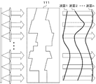
- a plane wave such as white light to be subjected to spectroscopy is converted into a wave having a different wavefront for each wavelength by passing through the scattering plate.
- the wavefronts of light having three wavelengths 1 to 3 included in the plane wave transmitted through the scattering plate are converted into different shapes by the scattering plate.
- the light whose wavefront is converted for each wavelength is reflected by a mirror having a mirror surface shaped so as to eliminate the difference in the optical path length at each location of the wavefront with respect to a specific wavelength, for example.
- the wavefront returns to a plane wave.
- FIG. 3A shows an example in which light of wavelength 2 returns to a plane wave among the light of three wavelengths 1 to 3.
- the wavefront shape for each wavelength is measured using, for example, a wavefront shape sensor.
- a mirror having a shape that eliminates the difference in optical path length at each position of the wavefront can be obtained by appropriately controlling a spatial light modulator (SLM) such as a variable shape mirror. That is, by controlling the mirror surface of the spatial light modulator according to the shape of the wavefront of the specific wavelength measured by the wavefront shape sensor, the light of the specific wavelength is returned to the plane wave. Further, when converted into wavefronts having different shapes for respective wavelengths, the wavefronts of light of other wavelengths have shapes different from those of plane waves.
- SLM spatial light modulator
- light having a wavefront of a specific wavelength described above passes through the optical system including the pinhole through the plane wave, so that the light of the wavefront other than the plane wave is scattered by the pinhole. That is, it is possible to form an image on a wavefront of a specific wavelength that has become a plane wave on the image sensor.
- a monochromatic image relating to the specific wavelength can be obtained by forming an image of the wavefront of the specific wavelength that has become a plane wave on the imaging element.
- FIG. 3 (B) light other than light of wavelength 2 which is a plane wave among light of three different wavelengths of wavelengths 1 to 3 is scattered by an optical system including a pinhole. That is, in this example, an image relating to wavelength 2 is obtained.
- the above procedure makes it possible to obtain a monochromatic image relating to a specific wavelength. And it becomes possible to obtain the image regarding many wavelengths by repeating said procedure with respect to several desired wavelength.
- the deformable mirror operates at an operating frequency of, for example, several kHz (kilohertz). That is, in the above-described procedure, for example, by using a deformable mirror as a spatial light modulator, it is possible to obtain a plane wave of light having several thousand wavelengths per second, for example.
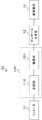
- FIG. 1 is a diagram illustrating a spectroscopic device according to the present embodiment.
- FIG. 2 is a diagram illustrating the imaging apparatus according to the present embodiment.
- the imaging device shown in FIG. 2 includes the spectroscopic device shown in FIG.
- the spectroscopic device 100 includes a modulation unit 110 and a demodulation unit 120.
- the modulator 110 converts the wavefront shape of light according to the wavelength.
- the demodulator 120 changes the phase of light having a specific wavelength selected from the light whose wavefront shape has been converted by the modulator 110 so as to be in a predetermined state.
- the demodulator 120 changes the phase of the light so that the light of which the wavefront shape has been converted by the modulator 110 is aligned with the light of a specific wavelength selected to become a plane wave.
- the imaging device 10 includes a collimator 11, the spectroscopic device 100 described above, a pinhole optical system 12, and an imaging element 13.
- the collimator 11 converts light related to a two-dimensional image of the object or the like into parallel light.
- the spectroscopic device 100 changes the phase of the selected light having a specific wavelength so as to be in a predetermined state such as parallel light, and emits the light.
- the pinhole optical system 12 forms an image on the imaging element 13 with the light converted into a plane wave by the spectroscopic device 100.
- the pinhole optical system 12 includes a pinhole.
- the image sensor 13 captures an image of light having a specific wavelength that is parallel light.
- the wavelength band of light targeted by the spectroscopic device 100 or the imaging device 10 is not limited.
- the spectroscopic device 100 or the imaging device 10 may target the wavelength band of visible light, or may target the wavelength band of infrared light or ultraviolet light.
- the image (wavefront) is decomposed into a plurality of two-dimensional pixels, for example, according to the pixels of the imaging element 13 or the like. That is, the modulation unit 110 converts the wavefront in units of, for example, a plurality of two-dimensional pixels according to the pixels of the image sensor 13 or the like.
- FIG. 4 shows an example of a specific configuration of the spectroscopic device 100 and the imaging device 10 having the spectroscopic device 100 in the present embodiment.
- the imaging device 10 according to the present embodiment includes a collimator 11, the spectroscopic device 100 described above, a pinhole optical system 12, and an imaging element 13.
- the scattering plate 111 is used as the modulation unit 110 of the spectroscopic device 100
- the variable shape mirror 121 is used as the demodulation unit 120.
- a block 16 that blocks the return light is provided as appropriate in order to avoid interference with the deformable mirror 121.
- the collimator 11 converts the light related to the two-dimensional image related to the object into parallel light.
- known means such as a collimator lens is used.
- a two-dimensional image incident on the collimator 11 is obtained by a lens 15 or the like as shown in FIG. In the example shown in FIG. 4, a lens 15 corresponding to the type of object is used as appropriate.
- the pinhole optical system 12 includes at least a pinhole.
- the pinhole optical system 12 forms an image of parallel light out of the light emitted from the spectroscopic device 100. That is, the pinhole optical system 12 scatters light that is not parallel light. In other words, the pinhole optical system 12 selectively transmits light having a wavelength that has been converted into parallel light by the spectroscopic device 100.
- the imaging element 13 images light having a wavelength that has been converted into parallel light by the spectroscopic device 100.
- a general image sensor such as a CMOS (Complementary Metal Oxide Semiconductor) image sensor or a CCD (Charge Coupled Device) is used as the image sensor 13.
- CMOS Complementary Metal Oxide Semiconductor
- CCD Charge Coupled Device
- the scattering plate 111 corresponding to the modulation unit 110 converts the wavefront shape according to the wavelength by utilizing the chromatic dispersion of the substance (that is, the difference in refractive index according to the wavelength of light). That is, the scattering plate 111 has a configuration in which the optical path length corresponding to the wavelength is different at least in part.
- the optical path length is represented by the product of the distance traveled by light when traveling through a medium and the refractive index of the medium.
- FIG. 5 shows an example in which the scattering plate 111 converts the wavefront shape.
- FIG. 5 shows a cross section of the scattering plate 111. That is, in the example of FIG. 5, it is assumed that the scattering plate 111 extends from the front to the back of the drawing.
- FIG. 5 shows an example in which parallel light is incident on the scattering plate 111 for each predetermined pixel via a microlens array such as an array of GRIN (Gradient Index) lenses. That is, in the example shown in FIG. 5, the light is reduced in diameter by the microlens array (squeezed sufficiently small with respect to the size of the pixel in the surface direction) to the left surface of the scattering plate 111 in FIG. Incident for each pixel.
- GRIN Gradient Index
- the light incident on the scattering plate 111 is converted by the scattering plate 111 so as to have different wavefront shapes for each of the wavefronts 1 through n (n is a natural number). That is, the scattering plate 111 converts the wavefront shape of light that is parallel light into a distorted wavefront that differs depending on the wavelength of the light.
- the light whose wavefront shape has been converted is emitted from the right surface of the scattering plate 111 in FIG.
- the shape of the contour of the surface on which the light of the scattering plate 111 enters or exits is appropriately determined according to the light incident on the scattering plate 111 or the like.
- the surface of the scattering plate 111 on which light enters or exits is, for example, rectangular.
- the deformable mirror 121 corresponding to the demodulator 120 is a mirror that can change the shape of the mirror surface.
- the variable shape mirror 121 changes the phase of the light of the selected wavelength among the light whose wavefront shape has been converted by the scattering plate 111 by changing the shape of the mirror surface. That is, the deformable mirror 121 has a mirror surface having a shape corresponding to the wavefront shape of the light. In this case, the deformable mirror 121 changes the phase so that the light of the selected wavelength becomes parallel light. . In this case, light of other wavelengths has a wavefront different from that of parallel light.
- variable shape mirror 121 makes it possible to change the phase so that a plurality of light beams having different wavelengths become parallel light by changing the shape of the mirror surface according to the wavefront shape for each wavelength.
- the shape of the mirror surface of the deformable mirror 121 is sequentially changed so that each of the light of a plurality of wavelengths becomes parallel light. Change the phase.
- the scattering plate 111 serving as the modulation unit 110 converts the wavefront shape of the parallel light related to the incident two-dimensional image according to the wavelength.
- the scattering plate 111 converts each wavefront shape of the plurality of wavelength lights to such an extent that the wavefront shapes can be distinguished by the variable shape mirror 121.
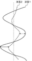
- the magnitude of the difference between any two wavefront shapes of a plurality of wavelength lights (that is, the difference in optical path length in at least one pixel) is It needs to be larger than the resolution. That is, when the difference in wavefront shape with respect to two wavelength lights indicated by the arrows in FIG. 6 is larger than the resolution of the shape variable mirror 121 in one or more pixels, the shape variable mirror 121 It becomes possible to change the phase individually.
- the deformable mirror 121 causes the light having the wavelength to be a plane wave. Cannot change the mirror surface. That is, in this case, it is difficult for the shape variable mirror 121 to change the phase of the wavefront so that the light of the wavelength becomes a plane wave. Therefore, when the wavefront shape is converted by the scattering plate 111, the difference in the optical path length for each pixel needs to be included in the movable range of the variable shape mirror 121 for each wavefront of light having a target wavelength. .
- An example of the relationship between the wavefront shape conversion by the scattering plate 111 and the number of wavelengths that can be distinguished by the variable shape mirror 121 is as follows. In this example, it is assumed that the resolution of the deformable mirror with respect to the incident direction of light is 1 nm (nanometer). In this case, if there is a difference of 1 nm or more in the optical path lengths of the wavefront shapes of the two wavelength lights, the wavefronts of the two wavelength lights are distinguished.
- the scattering plate 111 is quartz glass having a thickness of 1 mm (millimeter) and a wavelength from 340 nm to 900 nm is a measurement target.
- the difference in refractive index for light in the wavelength band is approximately 0.02692 based on the refractive index for light of 340 nm and the refractive index for light of 900 nm.
- the difference in optical path length for light in the wavelength band is obtained as 2.692 * 10 ⁇ 5 m (meters) by multiplying the difference in refractive index by the thickness of the scattering plate 111. “*” Means multiplication.
- the number of wavelengths (hereinafter sometimes referred to as “bands”) that can be distinguished by the deformable mirror 121 is the difference in optical path length. Is divided by the resolution of the deformable mirror 121 to obtain 26920 bands.
- the material used for the scattering plate 111 is not particularly limited.
- the scattering plate 111 is preferably formed of a material having high light transmittance and large chromatic dispersion, for example.
- the scattering plate 111 is formed of a material having a large chromatic dispersion, the difference in optical path length according to the wavelength is increased. That is, the difference in wavefront shape for each wavelength increases. And it becomes possible to distinguish light of a larger number of wavelengths.
- a material having a large chromatic dispersion generally varies depending on the wavelength.
- quartz glass is used.
- the near-infrared or mid-infrared is primarily intended, for example CaF 2 is (calcium fluoride) is used.
- ZnSe zinc selenide is used when medium infrared rays or far infrared rays are mainly targeted.
- the configuration of the scattering plate 111 are conceivable so that light of many wavelengths is converted into different wavefront shapes.
- the scattering plate 111 converts the light of multiple wavelengths into different wavefront shapes, so that the phase of the light of multiple wavelengths is aligned by the demodulator 120. That is, the scattering plate 111 converts light having a large number of wavelengths into different wavefront shapes, so that images having a large number of wavelengths can be acquired.
- the thickness of the surface of the scattering plate 111 may be changed depending on the part. That is, unevenness may be formed on the surface of the scattering plate 111.
- the thickness of the surface of the scattering plate 111 can be changed according to the portion of the surface of the scattering plate 111 such as for each pixel.
- the difference in optical path length for each wavelength changes. For example, when the thickness of the scattering plate 111 increases, the difference in optical path length for each wavelength increases in accordance with the thickness of the scattering plate 111. Therefore, when the thickness of the surface of the scattering plate 111 is changed depending on the part, the difference in the optical path length for each wavelength corresponding to the part of the scattering plate 111 increases.
- the scattering plate 111 may be formed by combining a plurality of layers of the same or different materials.
- the scattering plate 111 may be formed, for example, by bonding a plurality of layers of the same or different materials, or by providing a plurality of layers of the same or different materials at intervals. It may be formed.
- each of the plurality of layers is preferably made of a material having different color dispersion properties, for example.
- the difference in the optical path difference for each wavelength becomes larger than when the scattering plate 111 is formed of one material.
- the difference in wavefront shape for each wavelength increases. Therefore, it is possible to acquire images with more wavelengths.
- the thickness of the scattering plate 111 may be changed depending on the surface portion.
- the thickness of each layer forming the scattering plate 111 may be changed according to the surface portion.
- the scattering plate 111 may have a configuration in which the traveling direction of light is changed at least in part according to the wavelength. More specifically, the surface of the scattering plate 111 and the surface of each layer forming the scattering plate 111 are directed in a direction different from the direction perpendicular to the traveling direction of the parallel light incident on the scattering plate 111 depending on the part.
- the shape may extend.
- the surface of the scattering plate 111 may have a shape different from the planar shape.
- at least one of the surfaces of the scattering plate 111 may have a shape extending in a direction oblique to the traveling direction of parallel light incident on the scattering plate 111.
- the direction of the surface of the scattering plate 111 may be different for each part of the surface.
- the surface of the scattering plate 111 includes each surface of a plurality of layers forming the scattering plate 111.
- the traveling direction of the light passing through the scattering plate 111 (that is, the vector of the light beam) Orientation) can be changed. Further, the extending direction of the surface of the scattering plate 111 is changed in each of the surfaces of the scattering plate 111, whereby the traveling direction of light passing through each part of the surface of the scattering plate 111 is changed. For example, the traveling direction of the light passing through the scattering plate 111 is changed for each pixel on the surface of the scattering plate 111. Moreover, the change in the traveling direction of light varies depending on the wavelength.
- the traveling direction of light in each part of the wavefront changes for each wavelength. That is, the surface of the scattering plate 111 extends in an oblique direction with respect to the incident direction, so that the surface of the scattering plate 111 extends only in the direction perpendicular to the incident direction.
- a large difference is given to the wavefront shape for each wavelength.
- the number of wavelengths whose phases are adjusted by the variable shape mirror 121 can be increased.
- the roughness of the surface may be changed according to the site.
- the surface of the scattering plate 111 may have a different direction in which the surface extends depending on the part, or may have a different thickness depending on the part.
- the direction in which the surface extends may be different depending on the portion of the surface. In this case, each thickness may differ depending on the surface portion.
- FIG. 7A to 7C each show a cross-sectional view of a specific configuration example of the scattering plate 111.
- FIG. FIG. 7A shows an example in which the scattering plate 111 is formed of one material of the material 1.
- FIG. 7B shows an example in which the scattering plate 111 is formed of layers of two different materials, materials 1 and 2.
- FIG. 7C shows an example in which the scattering plate 111 is formed of layers of three different materials 1 to 3.
- parallel light is incident from the left side of each scattering plate 111 so as to be perpendicular to the left side surface of the scattering plate 111.
- the shape of one surface of the scattering plate 111 is different from the planar shape. That is, in the example of FIG. 7A, the shape of a part of one surface of the scattering plate 111 is formed so as to be inclined with respect to the traveling direction of the parallel light. In the example of FIG. 7A, the thickness of a part of one surface of the scattering plate 111 is different from the other parts. As an example, in the example of FIG. 7A, the lower part of the scattering plate 111 in the drawing has a larger thickness than other parts.
- the shape of the surface of the scattering plate 111 that is in contact with the layers of different materials is different from the planar shape as in the example of FIG. Yes.
- the materials 1 to 3 are not particularly limited.
- materials having different color dispersion are used.
- a material having different chromatic dispersion is used for the scattering plate, so that the difference in wavefront shape for each wavelength can be increased.
- each scattering plate 111 may have the various structures described above with respect to the depth direction in the drawing.
- the wavefront shape is converted by the scattering plate 111 so that the light of one pixel enters another pixel, there is a possibility that crosstalk occurs between the pixels. In order to avoid this, it is necessary to determine the traveling direction of the light of each pixel so that the light of each pixel does not enter the other pixels.
- FIG. 8 is a diagram relating to conditions of the light traveling direction in each pixel.
- the demodulator 120 is the deformable mirror 121
- the width of one pixel on the scattering plate 111 is c
- the distance from the surface of the scattering plate 111 on the deformable mirror 121 side to the mirror surface of the deformable mirror 121 is Assume that s.
- it is assumed that light incident on each pixel is reduced in diameter by, for example, a microlens array using a GRIN lens.
- the deformable mirror 121 that is the demodulator 120 is a mirror that can change the shape of the mirror surface by MEMS (Micro Electro Mechanical Systems) or an electromagnetic method. By changing the shape of the mirror surface, the deformable mirror 121 changes the phase of the wavefront.
- MEMS Micro Electro Mechanical Systems
- variable shape mirror is used as the variable shape mirror 121.
- the deformable mirror 121 is, for example, a deformable mirror whose surface shape is changed by a MEMS actuator.
- the mirror surface has a square shape with a side of 4 mm, and the number of actuators is 144.
- the distance between the actuators is 0.33 mm, and the resolution (shortest operating distance) is 1 nm.
- the operating frequency of the actuator is 8 kHz at maximum.
- the shape of the mirror surface is determined based on the operating distance of the actuator (that is, the movement distance of the actuator in the direction perpendicular to the mirror surface when the mirror surface is planar) and the distance between the actuators.
- the demodulator 120 is the variable shape mirror 121
- the number of wavelengths that can be dispersed per unit time is determined according to the operating frequency of the variable shape mirror 121.
- the operating frequency of the deformable mirror 121 is 8 kHz
- processing of 8000 bands can be performed in one second.
- the spectrum is performed in about 0.03 seconds. That is, in the spectroscopic device 100 according to the present embodiment, for example, the deformable mirror 121 is used as the demodulator 120, so that high-speed spectroscopy according to the operating frequency of the deformable mirror 121 is possible.
- the demodulator 120 may be realized by a different type of spatial light modulator from the deformable mirror 121.
- a spatial light modulator using liquid crystal is used as the demodulator 120.
- the phase is delayed according to the wavelength by controlling the liquid crystal.
- the phases of the light of the specific wavelength are aligned.
- the demodulation unit 120 may be realized using a technique based on the phase shift interferometry.
- a transfer function related to phase conversion by the scattering plate 111 is obtained based on a change in phase for each wavelength by the scattering plate 111 obtained in advance. And based on this transfer function, the light which wavefront shape was converted for every wavelength with the scattering plate 111 is imaged, and the process which changes the phase of the selected specific wavelength light with respect to the imaged image is performed. Is called.
- a series of processing is realized by an information processing apparatus such as a PC (Personal Computer).
- the demodulator 120 only needs to be able to change the phase so that light of the selected wavelength becomes a plane wave out of the light whose wavefront shape is converted according to the wavelength by the modulator 110.
- the demodulator 120 may be realized by a mechanism different from the deformable mirror 121.
- the mechanism used as the demodulator 120 may be appropriately determined according to the required operation speed and other conditions.
- the demodulator 120 is preferably a mechanism that can handle a large number of bands at high speed, such as the deformable mirror 121.
- Adjustment procedure of demodulator 120 In the spectroscopic device 100 according to the present embodiment, in order to align the phases of light of specific wavelengths, for example, when the deformable mirror 121 is used as the demodulator 120, the shape of the mirror surface of the deformable mirror 121 corresponding to the wavelength is determined. There is a need. When determining the shape of the mirror surface of the deformable mirror 121, it is necessary to grasp the wavefront shape for each wavelength. The wavefront shape converted by the scattering plate 111 that is the modulation unit 110 is obtained by the following procedure for each wavelength.
- FIG. 9 shows an example of a configuration used when adjusting the demodulation unit 120.
- monochromatic light having a specific wavelength, which is parallel light enters the scattering plate 111.
- the monochromatic light is obtained, for example, when white light is incident on the spectrophotometer 17 through the lens 15-1 or the like. Then, the monochromatic light thus obtained is incident on the collimator 11 through the lens 15-2 or the like, so that monochromatic light that is parallel light is obtained.
- the monochromatic light is converted into a wavefront shape corresponding to the wavelength by the scattering plate 111.
- the monochromatic light whose wavefront shape has been converted is introduced into the wavefront shape sensor 18.
- monochromatic light is introduced into the wavefront shape sensor 18 via the variable shape mirror 121.
- the deformable mirror 121 is controlled to be a flat surface.
- the monochromatic light whose wavefront shape has been converted may be directly introduced into the wavefront shape sensor 18 without passing through the variable shape mirror 121.
- the wavefront shape sensor 18 obtains the wavefront shape of the monochromatic light converted by the scattering plate 111.
- the shape of the mirror surface of the variable shape mirror 121 is obtained based on the obtained wavefront shape so that the light of the wavelength of the monochromatic light is a plane wave.
- the shape of the mirror surface of the deformable mirror 121 is obtained using a known method.
- the above-described operation is performed on monochromatic light of other wavelengths, so that the shape of the mirror surface of the deformable mirror 121 is obtained so that the monochromatic light of other wavelengths is a plane wave.
- Monochromatic light of other wavelengths is obtained by changing the diffraction wavelength of the spectrophotometer 17 or the like.
- the shape of the mirror surface of the deformable mirror 121 can be determined for a plurality of desired wavelengths by repeatedly performing the above-described operation for a plurality of wavelengths.
- the shape of the mirror surface of the variable shape mirror 121 is obtained for each of the scattering plates 111.
- the demodulator 120 changes the phase of light of a specific wavelength, information on the wavefront shape obtained as described above is appropriately used. Used.
- the demodulator 120 parallelizes the phase of light having a specific wavelength among the light whose wavefront shape is converted for each wavelength by the modulator 110 such as the scattering plate 111. It changes so that it may become predetermined
- the demodulator 120 uses a variable shape mirror 121 or the like.
- the deformable mirror 121 can operate at an operating frequency of several kHz. That is, by using the deformable mirror 121 in the demodulator 120, the spectroscopic device 100 can obtain, for example, plane waves of several thousand bands of light per second.
- the known hyperspectral imaging technique may require operations such as exchanging a filter for selecting a specific wavelength and scanning light dispersed by a diffraction grating during spectroscopy. If these operations are required when acquiring an image for each wavelength, it may take several seconds to acquire an image of one wavelength. In addition, a mechanism for these operations may be required.
- the spectroscopic device 100 according to the present embodiment enables high-speed spectroscopy. Moreover, the imaging device 10 having the spectroscopic device 100 according to the present embodiment can obtain images for a large number of wavelengths for hyperspectral imaging at high speed.
- spectroscopic device 100 Application example of spectroscopic device and imaging device
- the above-described spectroscopic device 100 and the imaging device 10 including the spectroscopic device 100 are applied to various fields.
- the imaging device 10 is used in the same manner as an existing device for hyperspectral imaging.
- the imaging device 10 is mounted on, for example, a satellite or an aircraft, and is used for environmental investigations.
- the imaging device 10 can obtain images for a number of wavelengths for hyperspectral imaging at high speed. For this reason, the imaging apparatus 10 is used for applications that require high-speed image acquisition.
- the imaging device 10 for security of an important facility or the like, it is possible to quickly identify a target object and to plan a quick countermeasure based on the identified information.
- the imaging device 10 is used for investigations of fires of chemical plants, pollutant emissions from factories, etc., so that the location of fires can be identified and the diffusion status of toxic substances can be observed and predicted. It becomes possible.
- the use of the imaging device 10 in fields such as life science and food science facilitates detailed analysis of chemical reactions and the like occurring inside cells and microorganisms.
- the imaging measure 10 facilitates analysis of the time course of these chemical reactions.
- the imaging device 10 when used as an endoscope or the like, it is possible to detect a disease or a resection site and to diagnose a state in a living body at high speed. This makes it possible to reduce the patient's pain.
- the imaging device 10 capable of detecting infrared rays is mounted on an automobile or the like, it is possible to recognize a person around the vehicle based on the radiation wavelength characteristics of the human body.
- the degree of freedom in operation is increased by obtaining images at high speed.
- the spectroscopic device 100 is used as a general spectroscopic device. Even in this case, the processing efficiency can be improved by performing high-speed spectroscopy.
- Appendix 1 Modulation means for converting the wavefront shape of light according to the wavelength;
- a spectroscopic device comprising demodulating means for changing the phase of light having a selected wavelength out of the light whose wavefront shape has been converted so as to be in a predetermined state.
- Appendix 2 The spectroscopic device according to appendix 1, wherein the demodulation unit changes the phase of the light having the selected wavelength so as to be parallel light.
- Appendix 3) The spectroscopic device according to appendix 1 or 2, wherein the modulation unit is a scattering plate having at least a part of an optical path length for each wavelength.
- Appendix 14 A collimator that makes the light related to the two-dimensional image the first parallel light;
- the spectroscopic device according to any one of appendices 1 to 13, wherein the phase of light having a specific wavelength among the first parallel light is changed to be parallel light;
- a pinhole optical system that forms an image of the second parallel light emitted from the spectroscopic device;
- An imaging apparatus comprising: an image sensor that images the second parallel light.
Landscapes
- Physics & Mathematics (AREA)
- Spectroscopy & Molecular Physics (AREA)
- General Physics & Mathematics (AREA)
- Spectrometry And Color Measurement (AREA)
- Mechanical Light Control Or Optical Switches (AREA)
- Studio Devices (AREA)
Abstract
高速な分光が可能な分光装置等を提供する。 分光装置は、波長に応じて光の波面形状を変換する変調手段と、波面形状を変換された光のうち、選択された波長の光の位相を所定の状態となるように変化させる復調手段とを備える。
Description
本発明は、分光装置及び撮像装置に関する。
ハイパースペクトルイメージングと呼ばれる、数十波長以上の多数の波長の画像を取得する技術が用いられつつある。ハイパースペクトルイメージング技術では、所望の波長帯の光を分光することで波長毎の画像が得られる。
ハイパースペクトルイメージング技術の一例が特許文献1に記載されている。特許文献1には、走査型投影表示装置等が記載されている。特許文献1に記載の走査型投影表示装置は、異なる波長領域の光が重ね合わされて入射した画像の1次元像を出射するスリット部材と、スリットからの出射光を走査して、二次元像をなす走査画像を生成する走査鏡を少なくとも備える。
ハイパースペクトルイメージング等においては、分光された個々の波長に関する画像の取得に長い時間が必要となる場合がある。すなわち、特許文献1に記載の技術等に対して、分光された画像の取得に要する時間等の更なる高速化が求められている。
本発明は、上記課題を解決するためになされたものであって、高速な分光が可能な分光装置等を提供することを 主たる目的とする。
本発明の一態様における分光装置は、波長に応じて光の波面形状を変換する変調手段と、波面形状を変換された光のうち、選択された特定の波長の光の位相を所定の状態となるように変化させる復調手段とを備える。
また、本発明の一態様における撮像装置は、二次元の画像に関する光を第1の平行光とするコリメータと、第1の平行光のうち、特定の波長の光の位相を平行光となるように変化させる分光装置と、分光装置から出射する第2の平行光を結像させるピンホール光学系と、第2の平行光を撮像するイメージセンサとを備える。
本発明によると、高速な分光が可能な分光装置等を提供することができる。
本発明の実施形態について、添付の図面を参照して説明する。なお、以下の説明では、「平面波」は、光の位相が等しい面(すなわち波面)が平面状である光を示す。本発明の実施形態においては、平面波には、実用上、平面波として扱うことが可能な程度の位相のずれや誤差を含む波(光)が含まれてもよい。また、本発明の実施形態において、「平行光」は、光線が平行に進む光をあらわす。平行光には、実用上、平行光として扱うことが可能な程度のずれや誤差を含む光が含まれてもよい。
(分光装置の原理)
次に、本実施形態における分光装置が用いる分光手法の原理について説明する。本実施形態における分光装置は、一つの観点では、補償光学の原理を用いて分光する。すなわち、本実施形態における分光装置100は、補償光学の原理が分光の技術に適用されたものであると考えることができる。
次に、本実施形態における分光装置が用いる分光手法の原理について説明する。本実施形態における分光装置は、一つの観点では、補償光学の原理を用いて分光する。すなわち、本実施形態における分光装置100は、補償光学の原理が分光の技術に適用されたものであると考えることができる。
図3を用いて、本実施形態における分光装置が用いる分光手法の原理の詳細を説明する。分光の対象となる白色光等の平面波は、散乱板を透過することによって、例えば波長毎に波面が異なる波に変換される。図3(A)に示す例では、散乱板を透過した平面波に含まれる波長1から3の3つの波長の光の波面が、散乱板によってそれぞれ異なる形状に変換されている。
このように波長毎に波面が変換された光が、例えば特定の波長に対して波面の各々の箇所における光路長の差をなくすような形状の鏡面を有する鏡に反射することで、当該波長の波面が平面波へ戻る。図3(A)では、波長1から3の3つの波長の光のうち、波長2の光が平面波へ戻る例が示されている。
波長毎の波面の形状は、例えば波面形状センサを用いて測定される。波面の各々の箇所における光路長の差をなくすような形状を有する鏡は、形状可変ミラー等の空間光変調器(Spatial Light Modulator:SLM)を適宜制御することで得られる。つまり、波面形状センサによって測定された特定の波長の波面の形状に応じて空間光変調器の鏡面を制御することで、特定の波長の光が平面波へ戻される。また、波長毎に異なる形状の波面に変換された場合には、他の波長の光の波面は平面波とは異なる形状となる。
そして、ピンホールを含む光学系に上述した特定の波長の波面が平面波となった光を通すことで、平面波以外の波面の光はピンホールによって散乱する。すなわち、平面波となった特定の波長の波面を撮像素子に結像させることが可能となる。平面波となった特定の波長の波面を撮像素子に結像させることで、当該特定の波長に関する単色の画像を得ることができる。図3(B)に示す例では、波長1から3の3つの異なる波長の光のうち、平面波である波長2の光以外の光がピンホールを含む光学系で散乱している。すなわち、この例では波長2に関する画像が得られる。
上記の手順によって、特定の波長に関する単色の画像を得ることが可能となる。そして、複数の所望の波長に対して上記の手順を繰り返すことで、多数の波長に関する画像を得ることが可能となる。
また、形状可変ミラーは、例えば数kHz(キロヘルツ)の動作周波数にて動作する。すなわち、上述した手順では、例えば空間光変調器として形状可変ミラーが用いられることで、例えば一秒間に数千波長の光の平面波を得ることが可能となる。
(分光装置及び撮像装置)
続いて、本発明の実施形態について説明する。図1は、本実施形態における分光装置を示す図である。図2は、本実施形態における撮像装置を示す図である。図2に示す撮像装置は、図1に示す分光装置を含む。
続いて、本発明の実施形態について説明する。図1は、本実施形態における分光装置を示す図である。図2は、本実施形態における撮像装置を示す図である。図2に示す撮像装置は、図1に示す分光装置を含む。
図1に示すとおり、本発明の第1の実施形態における分光装置100は、変調部110と、復調部120とを備える。変調部110は、波長に応じて光の波面形状を変換する。復調部120は、変調部110によって波面形状を変換された光のうち、選択された特定の波長の光の位相を所定の状態となるように変化させる。例えば、復調部120は、変調部110によって波面形状を変換された光のうち、選択された特定の波長の光を揃えて平面波となるように光の位相を変化させる。
また、図2に示すとおり、本発明の第1の実施形態における撮像装置10は、コリメータ11と、上述した分光装置100と、ピンホール光学系12と、撮像素子13とを有する。コリメータ11は、対象物等の二次元の画像に関する光を平行光とする。分光装置100は、コリメータ11で平行光とされた光が入射すると、選択された特定の波長の光の位相を例えば平行光等の所定の状態となるように変化させて出射する。ピンホール光学系12は、分光装置100によって平面波とされた光を撮像素子13に結像させる。ピンホール光学系12は、ピンホールを含む。撮像素子13は、平行光とされた特定の波長の光についての画像を撮像する。
なお、分光装置100又は撮像装置10にて対象とされる光の波長帯は限定されない。分光装置100又は撮像装置10は、可視光の波長帯を対象としてもよいし、赤外光や紫外光の波長帯を対象としてもよい。また、分光装置100又は撮像装置10において、画像(波面)は、撮像素子13の画素等に応じて、例えば二次元の複数の画素に分解される。つまり、変調部110は、撮像素子13の画素等に応じて、例えば二次元の複数の画素を単位に波面を変換する。
図4は、本実施形態における分光装置100及び分光装置100を有する撮像装置10の具体的な構成の一例を示す。図4に示すとおり、本実施形態における撮像装置10は、コリメータ11と、上述した分光装置100と、ピンホール光学系12と、撮像素子13とを有する。また、図4に示す例では、分光装置100の変調部110として散乱板111が用いられ、復調部120として形状可変ミラー121が用いられる。また、図4に示す例では、形状可変ミラー121での干渉を避けるため、戻り光を遮断するブロック16が適宜設けられている。
コリメータ11は、対象に関する二次元の画像に関する光を平行光とする。コリメータ11としては、コリメータレンズ等の既知の手段が用いられる。また、コリメータ11へ入射される二次元の画像は、例えば図4に示すように、レンズ15等によって得られる。図4に示す例では、対象の種類等に応じたレンズ15が適宜用いられる。
ピンホール光学系12は、少なくともピンホールを含む。ピンホール光学系12は、分光装置100が出射する光のうち、平行光を結像させる。つまり、ピンホール光学系12は、平行光ではない光を散乱させる。言い換えると、ピンホール光学系12は、分光装置100にて平行光とされた波長の光を選択的に透過させる。
撮像素子13は、分光装置100にて平行光とされた波長の光を撮像する。撮像素子13として、CMOS(Complementary Metal Oxide Semiconductor)イメージセンサやCCD(Charge Coupled Device)等の一般的なイメージセンサが用いられる。
変調部110に相当する散乱板111は、物質の色分散(すなわち、光の波長に応じた屈折率の差異)を利用して、波長に応じて波面形状を変換する。すなわち、散乱板111は、波長に応じた光路長が少なくとも一部で異なるような構成を有する。なお、光路長は、光がある媒質を進む際に、光が進む距離と、当該媒質の屈折率との積で表される。
図5は、散乱板111が波面形状を変換する場合の例を示す。図5では、散乱板111の断面が示されている。つまり、図5の例では、散乱板111が図の手前から奥へ延在している場合が想定されている。図5では、GRIN(Gradient Index)レンズのアレイ等のマイクロレンズアレイを介して、平行光が予め定められた画素毎に散乱板111へ入射する場合の例が示されている。すなわち、図5に示す例では、光は、マイクロレンズアレイによって細径化されて(画素の面方向に対する大きさに対して十分に小さく絞られて)散乱板111の図5における左側の面へ画素毎に入射する。そして、散乱板111へ入射した光は、散乱板111によって、波面1からn(nは自然数)の異なる波長の各々に対して異なる波面形状となるように変換される。すなわち、散乱板111は、平行光である光の波面形状を、光の波長に応じて異なる歪んだ波面となるように変換する。波面形状が変換された光は、散乱板111の図5における右側の面から出射する。散乱板111の光が入射又は出射する面の輪郭の形状は、散乱板111へ入射する光等に応じて適宜定められる。散乱板111の光が入射又は出射する面は、例えば矩形状とされる。
復調部120に相当する形状可変ミラー121は、鏡面の形状を変化させることができる鏡である。形状可変ミラー121は、鏡面の形状を変化させることで、散乱板111によって波面形状が変換された光のうち、選択された波長の光の位相を所定の状態となるように変化させる。すなわち、形状可変ミラー121は、鏡面を光の波面形状に応じた形状とすることで、この場合に、形状可変ミラー121は、選択された波長の光が平行光となるように位相を変化させる。この場合に、他の波長の光は平行光とは異なる波面となる。
また、形状可変ミラー121は、波長毎の波面形状に応じて鏡面の形状を変化させることで、複数の異なる波長の光が平行光となるように位相を変化させることを可能にする。この場合には、変調部110によって変換された波長毎の波面形状に応じて、形状可変ミラー121の鏡面の形状を例えば順次変化させることで、複数の波長の光の各々が平行光となるように位相を変化する。
(分光装置の構成の詳細)
次に、本実施形態における分光装置100の各構成要素の構成及び動作に関する条件の詳細について説明する。以下の説明では、変調部110は散乱板111であり、復調部120は形状可変ミラー121である場合が想定される。
次に、本実施形態における分光装置100の各構成要素の構成及び動作に関する条件の詳細について説明する。以下の説明では、変調部110は散乱板111であり、復調部120は形状可変ミラー121である場合が想定される。
最初に、変調部110について説明する。上述のように、変調部110である散乱板111は、入射された二次元の画像に関する平行光の波面形状を波長に応じて変換する。散乱板111は、複数の波長光の各々の波面形状が、形状可変ミラー121によって区別可能になる程度に各々の波面形状を変換する。具体的には、1つ以上の画素において、複数の波長光のうちの任意の2つの波面形状の差異(すなわち、少なくとも1つの画素における光路長の差異)の大きさが、形状可変ミラー121の分解能と比較して大きい必要がある。すなわち、図6の矢印で示される、2つの波長光に対する波面形状の差異が1つ以上の画素において形状可変ミラー121の分解能よりも大きい場合には、形状可変ミラー121は、2つの波長光の位相を個々に変化させることが可能となる。
また、特定の波長光に対する波面形状の画素毎の光路長の差が、形状可変ミラー121の鏡面の可動域よりも大きい場合には、形状可変ミラー121は、当該波長の光が平面波となるように鏡面を変更させることはできない。すなわち、この場合には、形状可変ミラー121によって、当該波長の光が平面波となるように波面の位相を変化させることは困難である。したがって、散乱板111によって波面形状が変換される場合に、対象とされる波長の光の波面の各々について、画素毎の光路長の差は、形状可変ミラー121の可動域に含まれる必要がある。
散乱板111による波面形状の変換と、形状可変ミラー121によって区別されうる波長の数との関係の例は以下のようになる。この例では、形状可変ミラーの光の入射方向に対する分解能が1nm(ナノメートル)である場合を想定する。この場合には、2つの波長光の波面形状の光路長に1nm以上の差異があれば、2つの波長光の波面が区別される。
また、この例では、散乱板111が、厚さが1mm(ミリメートル)の石英ガラスであり、340nmから900nmまでの波長が計測の対象とされる場合を想定する。この場合に、当該波長帯の光に対する屈折率の差は、340nmの光に対する屈折率及び900nmの光に対する屈折率に基づくと、約0.02692となる。そして、当該波長帯の光に対する光路長の差は、屈折率の差に散乱板111の厚みを乗じることで、2.692*10-5m(メートル)と求められる。なお、“*”は乗算を意味する。上述した光路長の差が形状可変ミラー121の可動域に含まれる場合には、形状可変ミラー121によって区別されうる波長(以下、「バンド」と称する場合がある)の数は、光路長の差を形状可変ミラー121の分解能で除して、26920バンドと求められる。
散乱板111に用いられる材質は特に制限されない。散乱板111は、例えば光の透過率が高く、かつ色分散が大きな材質にて形成されることが好ましい。散乱板111が色分散の大きな物質にて形成されることで、波長に応じた光路長の差異が大きくなる。すなわち、波長毎の波面形状の差異が大きくなる。そして、より多数の波長の光が区別可能となる。
色分散が大きな材質は、一般に波長によって異なる。可視光線が主な対象とされる場合には、例えば石英ガラスが用いられる。また、近赤外線又は中赤外線が主な対象とされる場合には、例えばCaF2(フッ化カルシウム)が用いられる。中赤外線又は遠赤外線が主な対象とされる場合には、例えばZnSe(セレン化亜鉛)が用いられる。
また、多数の波長の光が異なる波面形状に変換されるように、散乱板111の構成には様々な例が考えられる。散乱板111が多数の波長の光を異なる波面形状に変換することで、復調部120によって多数の波長の光の位相が揃えられる。すなわち、散乱板111が多数の波長の光を異なる波面形状に変換することで、多数の波長の画像の取得が可能となる。
一例として、散乱板111の面は、部位に応じて厚さが変えられてもよい。すなわち、散乱板111の面には、凹凸が形成されてもよい。散乱板111の面は、例えば画素毎等の散乱板111の面の部位に応じて厚さが変えられる。散乱板111の厚さが変わると、波長毎の光路長の差異が変化する。例えば散乱板111の厚みが大きくなると、波長毎の光路長の差異の大きさが散乱板111の厚みに応じて大きくなる。したがって、散乱板111の面の厚さが部位によって変えられることで、散乱板111の部位に応じた波長毎の光路長の差異が大きくなる。
また、散乱板111は、同一又は異なる材質の複数の層が組み合わされて形成されてもよい。この場合には、散乱板111は、例えば同一又は異なる材質の複数の層が貼り合わされる等にて形成されてもよいし、同一又は異なる材質の複数の層が間隔を空けて設けられることで形成されてもよい。
散乱板111が複数の層が組み合わされて形成される場合には、複数の層の各々は、例えば色分散の性質が異なる材質であることが好ましい。色分散の性質が異なる複数の材質が組み合わされることで、散乱板111がひとつの材質で形成される場合と比較して、波長毎の光路差の差異が大きくなる。その結果として、波長毎の波面形状の差異が大きくなる。したがって、より多くの波長の画像の取得が可能となる。
更に、複数の層が組み合わされて散乱板111が形成される場合においても、散乱板111は、面の部位によって厚さが変えられてもよい。この場合には、散乱版111を形成する各々の層の厚さが面の部位に応じて変えられてもよい。
また、散乱板111は、波長に応じて光の進行方向を少なくとも一部で変えるような構成を有してもよい。より詳しくは、散乱板111の面や散乱版111を形成する各々の層の面は、部位に応じて、散乱板111に入射される平行光の進行方向と垂直な方向とは異なる方向へ向かって延在するような形状でもよい。言い換えると、散乱板111の面は、平面状の形状とは異なる形状とされてもよい。例えば、散乱板111の面の少なくとも一つは、散乱板111に入射される平行光の進行方向に対して斜めとなる方向へ向かって延在するような形状でもよい。散乱板111の面は、面の部位毎に延在する方向が異なってもよい。なお、この場合において、散乱板111の面には、散乱板111を形成する複数の層の各々の面が含まれる。
散乱板111の面の延在方向が平行光の進行方向に垂直な方向とは異なる方向を向くような形状であることで、散乱板111を通過する光の進行方向(すなわち、光線のベクトルの向き)が変えられる。また、散乱板111の面の延在方向が散乱板111の面の各々において互いに変えられることで、散乱板111の面の各々の部位を通過する光の進行方向が変えられる。例えば、散乱板111を通過する光の進行方向が散乱板111の面の画素毎に変えられる。また、光の進行方向の変化は、波長に応じて異なる。すなわち、散乱板111が上述のような構成とされることで、波面の各々の部位における光の進行方向が波長毎に変化する。すなわち、散乱板111の面が入射方向に対して斜め方向の向きに延在することで、散乱板111の面が入射方向に対して垂直となる方向の向きのみに延在する場合と比較して、波長毎の波面形状には大きな差異が与えられる。そして、この結果として、形状可変ミラー121によって位相が揃えられる波長の数を増やすことが可能となる。
また、散乱板111の面(散乱板111を形成する複数の層の各々の面を含む)では、面の粗さが部位に応じて変えられてもよい。
散乱板111の面や散乱板111を構成する複数の層の各々の面は、更にこれらの構造が組み合わされてもよい。すなわち、散乱板111の面は、部位によって面が延在する向きが異なってもよいし、部位によって厚さが異なってもよい。また、異なる材質の複数の散乱板が組み合わされて散乱板111が形成される場合には、各々について、面の部位によって面が延在する向きが異なってもよい。この場合には、面の部位によって各々の厚さが異なってもよい。
図7の(A)から(C)の各々は、散乱板111の具体的な構成例の断面図を示す。図7(A)は、散乱板111が材質1の1つの材質にて形成されている例を示す。また、図7(B)は、散乱板111が材質1及び2の2つの異なる材質の層にて形成されている例を示す。同様に、図7(C)は、散乱板111が材質1から3の3つの異なる材質の層にて形成されている例を示す。なお、図7の例では、平行光が、各々の散乱板111の左側から、散乱板111の左側の面に垂直となるように入射する場合を想定する。
図7(A)では、散乱板111の1つの面の形状が、平面状の形状とは異なる形状とされている。すなわち、図7(A)の例では、散乱板111の1つの面の一部の形状が平行光の進行方向に対して斜めの方向を向くように形成されている。また、図7(A)の例では、散乱板111の1つの面の一部の厚みが他の部分とは異なるように形成されている。一例として、図7(A)の例では、散乱板111の図中下側の部分は、他の部分と比較して大きな厚みとされている。
また、図7(B)及び(C)の例では、散乱板111の異なる材質の層が接する面の形状が、図7(A)の例と同様に、平面状とは異なる形状とされている。このような形状とすることで、複数の波長の各々において、画素毎の光路長や光の進行方向に差異を与えることが可能となる。
なお、図7の例では、材質1から3の各々の材質は特に制限されないが、例えばそれぞれ色分散が異なる材質が用いられる。上述のように、色分散が異なる材質が散乱板に用いられることで、波長毎の波面形状の差異を大きくすることが可能となる。
なお、図7の各々の例では、散乱板111の断面図が示されている。しかしながら、各々の散乱板111の面等は、図中の奥行き方向に関しても上述した様々な構造を有してもよい。
また、散乱板111によって、1つの画素の光が他の画素に入り込む程度に波面形状が変換されると、画素間でのクロストークが生じる可能性がある。これを回避するためには、各々の画素の光が他の画素に入り込まないように各々の画素の光の進行方向が定められる必要がある。
図8は、各々の画素における光の進行方向の条件に関する図である。復調部120が形状可変ミラー121である場合において、散乱板111での1つの画素の幅がcであり、散乱板111の形状可変ミラー121側の面から形状可変ミラー121の鏡面までの距離がsである場合を想定する。この場合に、散乱板111によって進行方向が変えられた場合における各々の画素の光の進行方向に対する角度θは、tan(θ)=c/sとの関係を満たす必要がある。なお、この場合において、各々の画素へ入射する光は、例えばGRINレンズを用いたマイクロレンズアレイ等によって細径化されていることが想定される。
次に、復調部120について説明する。復調部120である形状可変ミラー121は、MEMS(Micro Electro Mechanical Systems)や電磁的手法によって、鏡面の形状を変化させることが可能な鏡である。鏡面の形状が変化することで、形状可変ミラー121は、波面の位相を変化させる。
本実施形態では、形状可変ミラー121として、例えば以下のような形状可変ミラーが用いられる。形状可変ミラー121は、例えば、MEMSアクチュエータによって鏡の表面形状が変化する形状可変ミラーである。この場合には、鏡面は1辺が4mmの正方形状であり、アクチュエータの数は144である。また、アクチュエータ間の距離は0.33mmとなり、分解能(最短の動作距離)は1nmである。アクチュエータの動作周波数は最大で8kHzである。アクチュエータの作動距離(すなわち、鏡面が平面状となる場合に鏡面に垂直となる方向へのアクチュエータの移動距離)及びアクチュエータの間隔に基づいて鏡面の形状が求められる。
復調部120が形状可変ミラー121である場合には、形状可変ミラー121の動作周波数に応じて、単位時間当たりに分光可能な波長数が定められる。上述のように、形状可変ミラー121の動作周波数が8kHzである場合には、1秒間で8000バンドの処理が可能となる。例えば、二次元の画像に対して250バンドの分光が必要とされる場合には、約0.03秒で分光が行われる。すなわち、本実施形態における分光装置100では、復調部120として例えば形状可変ミラー121が用いられることで、形状可変ミラー121の動作周波数に応じた高速な分光が可能となる。
なお、復調部120は、形状可変ミラー121とは異なる種類の空間光変調器等にて実現されてもよい。例えば、復調部120として、液晶を用いた空間光変調器が用いられる。この場合には、液晶の制御によって、波長に応じて位相に遅延が与えられる。特定の波長光の波面に応じた遅延が与えられることで、当該特定の波長の光の位相が揃えられる。
また、復調部120は、位相シフト干渉法に基づく手法を用いて実現されてもよい。この場合には、予め求められた散乱板111による波長毎の位相の変化に基づいて、散乱板111による位相の変換に関する伝達関数が求められる。そして、この伝達関数に基づいて、散乱板111によって波長毎に波面形状が変換された光を撮像し、撮像された画像に対して、選択された特定の波長光の位相を変化させる処理が行われる。一連の処理は、PC(Personal Computer)等の情報処理装置にて実現される。
すなわち、復調部120は、変調部110によって波長に応じて波面形状が変換された光のうち、選択された波長の光が平面波となるように位相を変化させることが可能であればよい。この場合には、復調部120は、形状可変ミラー121とは異なる機構によって実現されてもよい。復調部120として用いられる機構は、必要とされる動作速度等やその他の条件に応じて適宜定められればよい。復調部120は、形状可変ミラー121のように、多数のバンドを高速に扱える機構であることが好ましい。
(復調部120の調整手順)
本実施形態における分光装置100では、特定の波長の光の位相を揃えるために、例えば復調部120として形状可変ミラー121が用いられる場合には波長に応じた形状可変ミラー121の鏡面の形状を定める必要がある。そして、形状可変ミラー121の鏡面の形状を定める際には、波長毎の波面形状の把握が必要となる。変調部110である散乱板111にて変換される波面形状は、波長毎に以下の手順にて求められる。図9は、復調部120の調整に際して用いられる構成の例を示す。
本実施形態における分光装置100では、特定の波長の光の位相を揃えるために、例えば復調部120として形状可変ミラー121が用いられる場合には波長に応じた形状可変ミラー121の鏡面の形状を定める必要がある。そして、形状可変ミラー121の鏡面の形状を定める際には、波長毎の波面形状の把握が必要となる。変調部110である散乱板111にて変換される波面形状は、波長毎に以下の手順にて求められる。図9は、復調部120の調整に際して用いられる構成の例を示す。
まず、平行光である特定の波長の単色光が散乱板111へ入射する。単色光は、例えば白色光をレンズ15-1等を介して分光光度計17へ入射する等によって得られる。そして、このように得られた単色光がレンズ15-2等を介してコリメータ11へ入射される等によって、平行光である単色光が得られる。平行光である単色光が散乱板111へ入射されると、単色光は、散乱板111によって波長に応じた波面形状へ変換される。
続いて、波面形状が変換された単色光は、波面形状センサ18へ導入される。図9に示す例では、単色光は形状可変ミラー121を介して波面形状センサ18へ導入される。この例では、形状可変ミラー121は平面となるように制御される。なお、波面形状が変換された単色光は、形状可変ミラー121を介さずに直接に波面形状センサ18へ導入されてもよい。そして、波面形状センサ18によって、散乱板111によって変換された単色光の波面形状が求められる。
そして、波面形状が求められると、求められた波面形状に基づいて、当該単色光の波長の光を平面波とするような形状可変ミラー121の鏡面の形状が求められる。この場合には、形状可変ミラー121の鏡面の形状は、既知の手法を用いて求められる。
上述の動作が他の波長の単色光に対して行われることで、当該他の波長の単色光を平面波とするような形状可変ミラー121の鏡面の形状が求められる。他の波長の単色光は、分光光度計17の回折波長を変える等によって得られる。すなわち、上述の動作が複数の波長に対して繰返し行われることで、所望の複数の波長に対して形状可変ミラー121の鏡面の形状を定められる。
なお、異なる散乱板111が用いられる場合には、形状可変ミラー121の鏡面の形状が散乱板111の各々に対して求められる。また、復調部120として形状可変ミラー121以外の機構が用いられる場合において、復調部120が特定の波長の光の位相を変化させる際には、上述のように得られた波面形状に関する情報が適宜用いられる。
以上のとおり、本実施形態における分光装置100は、散乱板111等の変調部110にて波長毎に波面形状が変換された光のうち、特定の波長の光の位相を復調部120が例えば平行光等の所定の状態となるように変化させる。このようにすることで、本実施形態における分光装置100は、特定の波長に対する画像の取得を可能とする。
また、復調部120には、形状可変ミラー121等が用いられる。形状可変ミラー121は、数kHzの動作周波数での動作が可能である。すなわち、復調部120に形状可変ミラー121が用いられることで、分光装置100は、例えば一秒間に数千バンドの光の平面波を得ることを可能とする。
これに対して、既知のハイパースペクトルイメージング技術では、分光に際して、特定の波長を選択するフィルタの交換や、回折格子によって分光された光の走査等の動作が必要となる場合がある。波長毎の画像の取得に際してこれらの動作が必要となる場合には、1つの波長の画像の取得に数秒程度の時間を要する場合がある。また、これらの動作のための機構が必要となる場合がある。
すなわち、本実施形態における分光装置100は、高速な分光を可能とする。また、本実施形態における分光装置100を有する撮像装置10は、ハイパースペクトルイメージングのための多数の波長に対する画像を高速に得ることを可能とする。
(分光装置及び撮像装置の適用例)
上述した分光装置100及び分光装置100を備える撮像装置10は、種々の分野へ適用される。
上述した分光装置100及び分光装置100を備える撮像装置10は、種々の分野へ適用される。
一例として、撮像装置10は、既存のハイパースペクトルイメージングのための装置と同様に用いられる。撮像装置10は、例えば衛星や航空機等に搭載されて、環境の調査等に用いられる。
また、上述のように、撮像装置10は、ハイパースペクトルイメージングのための多数の波長に対する画像を高速に得ることを可能とする。そのため、撮像装置10は、高速な画像の取得が必要とされる用途に関して用いられる。
例えば、重要な施設の警備等に撮像装置10が用いられることで、目標物の迅速かつ詳細な識別や、識別された情報に基づく迅速な対策の立案が可能となる。
別の例として、化学プラント等の火災や工場等からの汚染物質の排出の調査等に関して撮像装置10が用いられることで、火災の発生箇所の特定、有毒な物質の拡散状況の観測や予測が可能となる。
また、生命科学や食品科学等の分野に撮像装置10が用いられることで、細胞や微生物の内部で生じる化学反応等の詳細な分析が容易になる。特に、撮像措置10によって、これらの化学反応の時間的な経過の分析が容易になる。これと類似して、内視鏡等として撮像装置10が用いられる場合には、疾患や切除部位の検出や生体内の状態の高速な診断が可能となる。これによって、患者の苦痛の軽減が可能となる。
更に、赤外線の検知が可能な撮像装置10が自動車等に搭載されることで、人体の放射波長特性に基づいた、運転中の周囲の人物の認識が可能となる。
この他に、撮像装置10が既存のハイパースペクトルイメージングのための装置と同様に用いられる場合においても、画像が高速に得られることで、運用の自由度が高められる。
また、分光装置100は、一般的な分光装置として用いられる。この場合においても、高速な分光が行われることで、処理の効率化が可能となる。
以上、実施形態を参照して本発明を説明したが、本発明は上記実施形態に限定されるものではない。本発明の構成や詳細には、本発明のスコープ内で当業者が理解し得る様々な変更をすることができる。また、各実施形態における構成は、本発明のスコープを逸脱しない限りにおいて、互いに組み合わせることが可能である。
この出願は、2016年10月12日に出願された日本出願特願2016-201022を基礎とする優先権を主張し、その開示の全てをここに取り込む。
この発明の一部又は全部は、以下の付記のようにも表されるが、以下に限られない。
(付記1)
波長に応じて光の波面形状を変換する変調手段と、
前記波面形状を変換された光のうち、選択された波長の光の位相を所定の状態となるように変化させる復調手段とを備える分光装置。
(付記2)
前記復調手段は、前記選択された波長の光の位相を平行光となるように変化させる、付記1に記載の分光装置。
(付記3)
前記変調手段は、波長毎の光路長が少なくとも一部で異なる散乱板である、付記1又は2に記載の分光装置。
(付記4)
前記散乱板は、前記光の進行方向に対する厚さが異なる部位を含む、付記3に記載の分光装置。
(付記5)
前記散乱板の前記光が入射又は出射する面に凹凸が形成されている、付記3又は4に記載の分光装置。
(付記6)
前記散乱板は、波長に応じて前記光の進行方向を少なくとも一部で変化させる、付記3から5のいずれか一項に記載の分光装置。
(付記7)
前記散乱板は、前記光が入射又は出射する面が前記光の進行方向に対して斜めとなる方向に延在する部位を含む、付記3から6のいずれか一項に記載の分光装置。
(付記8)
前記散乱板は複数の層を有する、付記3から7のいずれか一項に記載の分光装置。
(付記9)
前記複数の層の少なくとも一つの層は、他の層と異なる材料で形成されている、付記8に記載の分光装置。
(付記10)
前記復調手段は空間光変調器である、付記1から9のいずれか一項に記載の分光装置。
(付記11)
前記空間光変調器は形状可変ミラーである、付記10に記載の分光装置。
(付記12)
前記空間光変調器は液晶空間光変調素子である、付記10に記載の分光装置。
(付記13)
前記復調手段は、位相シフト干渉法に基づいて前記位相を所定の状態となるように変化させる、付記1から9のいずれか一項に記載の分光装置。
(付記14)
二次元の画像に関する光を第1の平行光とするコリメータと、
前記第1の平行光のうち、特定の波長の光の位相を平行光となるように変化させる付記1から13のいずれか一項に記載の分光装置と、
前記分光装置から出射する第2の平行光を結像させるピンホール光学系と、
前記第2の平行光を撮像するイメージセンサとを備える撮像装置。
100 分光装置
110 変調部
120 復調部
10 撮像装置
11 コリメータ
12 ピンホール光学系
13 撮像素子
15 レンズ
16 ブロック
110 変調部
120 復調部
10 撮像装置
11 コリメータ
12 ピンホール光学系
13 撮像素子
15 レンズ
16 ブロック
Claims (14)
- 波長に応じて光の波面形状を変換する変調手段と、
前記波面形状を変換された光のうち、選択された波長の光の位相を所定の状態となるように変化させる復調手段とを備える分光装置。 - 前記復調手段は、前記選択された波長の光の位相を平行光となるように変化させる、請求項1に記載の分光装置。
- 前記変調手段は、波長毎の光路長が少なくとも一部で異なる散乱板である、請求項1又は2に記載の分光装置。
- 前記散乱板は、前記光の進行方向に対する厚さが異なる部位を含む、請求項3に記載の分光装置。
- 前記散乱板の前記光が入射又は出射する面に凹凸が形成されている、請求項3又は4に記載の分光装置。
- 前記散乱板は、波長に応じて前記光の進行方向を少なくとも一部で変化させる、請求項3から5のいずれか一項に記載の分光装置。
- 前記散乱板は、前記光が入射又は出射する面が前記光の進行方向に対して斜めとなる方向に延在する部位を含む、請求項3から6のいずれか一項に記載の分光装置。
- 前記散乱板は複数の層を有する、請求項3から7のいずれか一項に記載の分光装置。
- 前記複数の層の少なくとも一つの層は、他の層と異なる材料で形成されている、請求項8に記載の分光装置。
- 前記復調手段は空間光変調器である、請求項1から9のいずれか一項に記載の分光装置。
- 前記空間光変調器は形状可変ミラーである、請求項10に記載の分光装置。
- 前記空間光変調器は液晶空間光変調素子である、請求項10に記載の分光装置。
- 前記復調手段は、位相シフト干渉法に基づいて前記位相を所定の状態となるように変化させる、請求項1から9のいずれか一項に記載の分光装置。
- 二次元の画像に関する光を第1の平行光とするコリメータと、
前記第1の平行光のうち、特定の波長の光の位相を平行光となるように変化させる請求項1から13のいずれか一項に記載の分光装置と、
前記分光装置から出射する第2の平行光を結像させるピンホール光学系と、
前記第2の平行光を撮像するイメージセンサとを備える撮像装置。
Priority Applications (2)
| Application Number | Priority Date | Filing Date | Title |
|---|---|---|---|
| JP2018544725A JPWO2018070206A1 (ja) | 2016-10-12 | 2017-09-21 | 分光装置及び撮像装置 |
| US16/341,133 US10908021B2 (en) | 2016-10-12 | 2017-09-21 | Spectroscopic device and imaging device |
Applications Claiming Priority (2)
| Application Number | Priority Date | Filing Date | Title |
|---|---|---|---|
| JP2016201022 | 2016-10-12 | ||
| JP2016-201022 | 2016-10-12 |
Publications (1)
| Publication Number | Publication Date |
|---|---|
| WO2018070206A1 true WO2018070206A1 (ja) | 2018-04-19 |
Family
ID=61905325
Family Applications (1)
| Application Number | Title | Priority Date | Filing Date |
|---|---|---|---|
| PCT/JP2017/034067 WO2018070206A1 (ja) | 2016-10-12 | 2017-09-21 | 分光装置及び撮像装置 |
Country Status (3)
| Country | Link |
|---|---|
| US (1) | US10908021B2 (ja) |
| JP (1) | JPWO2018070206A1 (ja) |
| WO (1) | WO2018070206A1 (ja) |
Families Citing this family (2)
| Publication number | Priority date | Publication date | Assignee | Title |
|---|---|---|---|---|
| CN114594587B (zh) * | 2020-12-07 | 2023-06-09 | 中国科学院长春光学精密机械与物理研究所 | 一种紫外巡天的光学成像系统 |
| JP2023025742A (ja) * | 2021-08-11 | 2023-02-24 | 株式会社ディスコ | 光照射装置 |
Citations (10)
| Publication number | Priority date | Publication date | Assignee | Title |
|---|---|---|---|---|
| JP2001036471A (ja) * | 1999-07-15 | 2001-02-09 | Mitsubishi Electric Corp | 波面誤差検出装置及び波面誤差検出方法 |
| JP2002525596A (ja) * | 1998-09-23 | 2002-08-13 | アイシス イノヴェイション リミテッド | 波面感知装置 |
| JP2002544553A (ja) * | 1999-05-18 | 2002-12-24 | キャンパス テクノロジーズ アーゲー | 光信号検出または生成装置 |
| US20030053052A1 (en) * | 2001-09-19 | 2003-03-20 | Braun David M. | Optical monochromators having time dispersion correction |
| JP2005512075A (ja) * | 2001-12-10 | 2005-04-28 | ザイゴ コーポレーション | 位相シフト干渉分析の方法及びシステム |
| JP2009526984A (ja) * | 2006-02-16 | 2009-07-23 | オーエヌウエールア(オフィス ナショナル デチュード エ ドゥ ルシェルシュ アエロスパシアル) | 周波数差マルチラテラル干渉法を通じて波面を解析する方法 |
| JP2011053150A (ja) * | 2009-09-03 | 2011-03-17 | Nikon Corp | 波面測定方法及び波面測定装置 |
| CN102818631A (zh) * | 2012-07-30 | 2012-12-12 | 中国科学院上海光学精密机械研究所 | 基于随机波前相位调制的压缩光谱成像系统 |
| WO2016056147A1 (ja) * | 2014-10-08 | 2016-04-14 | オリンパス株式会社 | 結像光学系、照明装置および観察装置 |
| JP2016168192A (ja) * | 2015-03-12 | 2016-09-23 | キヤノン株式会社 | 画像撮像装置及びその制御方法 |
Family Cites Families (3)
| Publication number | Priority date | Publication date | Assignee | Title |
|---|---|---|---|---|
| US6735012B2 (en) * | 2002-03-22 | 2004-05-11 | The Boeing Company | System for phase modulating an incoming optical wavefront |
| JP2015055819A (ja) | 2013-09-13 | 2015-03-23 | 株式会社トプコン | 走査型投影表示光学系、および走査型投影表示装置 |
| DE112015003924T5 (de) * | 2014-10-03 | 2017-05-18 | Olympus Corporation | Mikroskopvorrichtung zum Scannen in die Richtung der optischen Achse |
-
2017
- 2017-09-21 JP JP2018544725A patent/JPWO2018070206A1/ja active Pending
- 2017-09-21 WO PCT/JP2017/034067 patent/WO2018070206A1/ja active Application Filing
- 2017-09-21 US US16/341,133 patent/US10908021B2/en active Active
Patent Citations (10)
| Publication number | Priority date | Publication date | Assignee | Title |
|---|---|---|---|---|
| JP2002525596A (ja) * | 1998-09-23 | 2002-08-13 | アイシス イノヴェイション リミテッド | 波面感知装置 |
| JP2002544553A (ja) * | 1999-05-18 | 2002-12-24 | キャンパス テクノロジーズ アーゲー | 光信号検出または生成装置 |
| JP2001036471A (ja) * | 1999-07-15 | 2001-02-09 | Mitsubishi Electric Corp | 波面誤差検出装置及び波面誤差検出方法 |
| US20030053052A1 (en) * | 2001-09-19 | 2003-03-20 | Braun David M. | Optical monochromators having time dispersion correction |
| JP2005512075A (ja) * | 2001-12-10 | 2005-04-28 | ザイゴ コーポレーション | 位相シフト干渉分析の方法及びシステム |
| JP2009526984A (ja) * | 2006-02-16 | 2009-07-23 | オーエヌウエールア(オフィス ナショナル デチュード エ ドゥ ルシェルシュ アエロスパシアル) | 周波数差マルチラテラル干渉法を通じて波面を解析する方法 |
| JP2011053150A (ja) * | 2009-09-03 | 2011-03-17 | Nikon Corp | 波面測定方法及び波面測定装置 |
| CN102818631A (zh) * | 2012-07-30 | 2012-12-12 | 中国科学院上海光学精密机械研究所 | 基于随机波前相位调制的压缩光谱成像系统 |
| WO2016056147A1 (ja) * | 2014-10-08 | 2016-04-14 | オリンパス株式会社 | 結像光学系、照明装置および観察装置 |
| JP2016168192A (ja) * | 2015-03-12 | 2016-09-23 | キヤノン株式会社 | 画像撮像装置及びその制御方法 |
Also Published As
| Publication number | Publication date |
|---|---|
| US20190242749A1 (en) | 2019-08-08 |
| JPWO2018070206A1 (ja) | 2019-08-29 |
| US10908021B2 (en) | 2021-02-02 |
Similar Documents
| Publication | Publication Date | Title |
|---|---|---|
| US11415460B2 (en) | Fabry-Perot Fourier transform spectrometer | |
| EP1613922B1 (en) | Methods and systems for static multimode multiplex spectroscopy | |
| JP6386614B2 (ja) | フルフレームのプログラム可能なハイパースペクトルイメージャ | |
| JP5635624B2 (ja) | 小型干渉分光計 | |
| US11002601B2 (en) | Spectroscopic microscope and spectroscopic observation method | |
| US11725989B2 (en) | Microelectromechanical system (MEMS) and (MEM) optical interferometer for hyper-spectral imaging and analysis | |
| JP2009265101A (ja) | 光ビームの波面を解析するための方法、位相格子および装置 | |
| WO2018070206A1 (ja) | 分光装置及び撮像装置 | |
| US20050122529A1 (en) | Measurement system of three-dimensional shape of transparent thin film using acousto-optic tunable filter | |
| JP5563405B2 (ja) | 分光画像取得装置及び方法 | |
| US10379275B2 (en) | Optical filter including plates for filtering light and optical measuring device employing optical filter | |
| JP5371362B2 (ja) | レーザ顕微鏡装置 | |
| JP2008008842A (ja) | 電磁波測定装置 | |
| US20220229213A1 (en) | Diffraction element and imaging device | |
| WO2021044979A1 (ja) | 分光測定装置 | |
| AU2015261653B2 (en) | Fabry-Perot Fourier transform spectrometer | |
| JP3740571B2 (ja) | 2次元画像の分光方法及び装置 | |
| WO2023176638A1 (ja) | 光学装置 | |
| KR20040004825A (ko) | 음향광학변조필터를 이용한 투명박막의 3차원 형상측정장치 | |
| RU2673784C1 (ru) | Двухкомпонентный интерферометр общего пути | |
| Asuka et al. | Spectroscopic-tomography of biological membrane with high-spatial resolution by the imaging-type 2D Fourier spectroscopy | |
| WO2022234588A1 (en) | Systems and methods to acquire three dimensional images using spectral information | |
| JP2015169584A (ja) | 分光分析装置 |
Legal Events
| Date | Code | Title | Description |
|---|---|---|---|
| 121 | Ep: the epo has been informed by wipo that ep was designated in this application |
Ref document number: 17859922 Country of ref document: EP Kind code of ref document: A1 |
|
| ENP | Entry into the national phase |
Ref document number: 2018544725 Country of ref document: JP Kind code of ref document: A |
|
| NENP | Non-entry into the national phase |
Ref country code: DE |
|
| 122 | Ep: pct application non-entry in european phase |
Ref document number: 17859922 Country of ref document: EP Kind code of ref document: A1 |