WO2018066286A1 - ビーム走査装置およびパターン描画装置 - Google Patents
ビーム走査装置およびパターン描画装置 Download PDFInfo
- Publication number
- WO2018066286A1 WO2018066286A1 PCT/JP2017/031737 JP2017031737W WO2018066286A1 WO 2018066286 A1 WO2018066286 A1 WO 2018066286A1 JP 2017031737 W JP2017031737 W JP 2017031737W WO 2018066286 A1 WO2018066286 A1 WO 2018066286A1
- Authority
- WO
- WIPO (PCT)
- Prior art keywords
- reflected
- scanning
- polygon mirror
- reflecting surface
- origin
- Prior art date
- Legal status (The legal status is an assumption and is not a legal conclusion. Google has not performed a legal analysis and makes no representation as to the accuracy of the status listed.)
- Ceased
Links
Images






Classifications
-
- G—PHYSICS
- G02—OPTICS
- G02B—OPTICAL ELEMENTS, SYSTEMS OR APPARATUS
- G02B26/00—Optical devices or arrangements for the control of light using movable or deformable optical elements
- G02B26/08—Optical devices or arrangements for the control of light using movable or deformable optical elements for controlling the direction of light
- G02B26/10—Scanning systems
- G02B26/12—Scanning systems using multifaceted mirrors
-
- G—PHYSICS
- G02—OPTICS
- G02B—OPTICAL ELEMENTS, SYSTEMS OR APPARATUS
- G02B26/00—Optical devices or arrangements for the control of light using movable or deformable optical elements
- G02B26/08—Optical devices or arrangements for the control of light using movable or deformable optical elements for controlling the direction of light
- G02B26/10—Scanning systems
Definitions
- the present invention relates to a beam scanning device that scans a spot light of a beam irradiated on an irradiated surface of an object, and a pattern drawing device that draws and exposes a predetermined pattern using such a beam scanning device.
- spot light of a laser beam is projected onto an object to be irradiated (processing object), and the object to be irradiated is orthogonal to the main scanning direction while the spot light is main-scanned in a one-dimensional direction by a scanning mirror (polygon mirror).
- a laser processing apparatus for example, JP-A-2005-262260 shown below
- an optical scanning device It is known to use an optical scanning device.
- Japanese Patent Application Laid-Open No. 2005-262260 discloses a galvano that corrects the irradiation position on the workpiece by reflecting the laser beam from the oscillator 1 in the Y direction (sub-scanning direction).
- a mirror a polygon mirror that reflects the laser beam reflected by the galvanometer mirror and scans the workpiece in the X direction (main scanning direction), and the laser beam reflected by the galvanometer mirror is condensed on the workpiece.
- the reflection angle of the galvanometer mirror so as to correct the irradiation position error of the laser beam on the workpiece in correspondence with the distortion generated when the laser beam passes through the f ⁇ lens.
- FIG. 8 of Japanese Patent Laid-Open No. 2005-262260 shows a laser light source that emits a detection laser beam for detecting the end of each reflecting surface of the polygon mirror while the polygon mirror is rotating, and each reflecting surface of the polygon mirror.
- a detector for receiving the reflected light of the detection laser beam reflected at the end of the laser and generating an end detection signal is provided, and the timing of pulse oscillation in the oscillator based on the end detection signal is shown in FIG.
- the configuration to be controlled is shown in FIG.
- a scanning optical system in which a processing beam deflected by a reflection surface of a scanning member having a variable angle is incident, and the processing beam is condensed as a spot on an irradiated body.
- a beam scanning device that scans the spot at a scanning speed according to a change in the angle of the reflection surface of the scanning member, and a detection beam for detecting an origin at which the reflection surface of the scanning member is at a predetermined angle.
- a beam transmitting unit that projects onto the reflecting surface of the scanning member; a beam reflecting unit that receives the detection beam reflected by the reflecting surface of the scanning member and reflects the beam toward the reflecting surface of the scanning member; A beam receiving unit that receives the reflected beam of the detection beam reflected second time on the reflecting surface of the scanning member and outputs an origin signal indicating the origin.
- the scanning optical system includes a drawing optical beam that is incident on a drawing beam deflected by a reflection surface of a scanning member having a variable angle and collects the drawing beam as a spot on a substrate.
- a pattern drawing apparatus for drawing a pattern on the substrate by modulating the intensity of the drawing beam according to a pattern while scanning the spot at a scanning speed corresponding to an angle change of a reflection surface of a member,
- a beam transmitting unit for projecting a detection beam for detecting an origin at which the reflection surface of the scanning member has a predetermined angle onto the reflection surface of the scanning member, and the detection beam reflected by the reflection surface of the scanning member are incident.
- Output Comprising a chromatography arm receiving portion, and a control unit for controlling the writing of the pattern by the spot on the basis of the origin signal.
- a processing beam deflected by one of a plurality of reflecting surfaces of a rotary polygon mirror is condensed as a spot on an irradiated object by a scanning optical system, and the rotary polygon A beam scanning device that scans the spot by rotating a mirror, wherein a detection beam for detecting an origin at which each of a plurality of reflecting surfaces of the rotating polygon mirror has a predetermined angle is applied to the reflecting surface of the rotating polygon mirror.
- a beam transmitting unit to project a beam reflecting unit that receives the detection beam reflected by the reflecting surface of the rotating polygon mirror and reflects the reflected beam toward the reflecting surface of the rotating polygon mirror, and a reflection of the rotating polygon mirror
- a beam receiving unit that receives the reflected beam of the detection beam reflected on the surface for the second time and outputs an origin signal representing the origin.
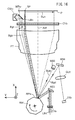
- FIG. 3 is a view of the arrangement of a polygon mirror, an optical axis of an f ⁇ lens system, a beam transmitting unit that constitutes an origin sensor, a beam receiving unit, and the like in a drawing unit illustrated in FIG. 2 in a plane parallel to an XY plane.
- FIG. 3 shows the detailed structure of the photoelectric conversion element (photoelectric detector) provided in a beam light-receiving part.
- FIG. 4 is a plan view of the eight-sided polygon mirror shown in FIGS. 1 to 3; It is a figure explaining the method to measure the reproducibility (variation) of the origin signal generation timing. It is the figure which represented typically the method of estimating the time error part by the speed fluctuation
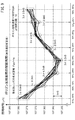
- FIG. 9 is a graph showing the results of actually measuring the reproducibility of the origin signal generated corresponding to each of the reflecting surfaces of the polygon mirror by a method as shown in FIGS. 7 and 8 under a predetermined condition.
- FIG. 9 is a graph showing the results of actually measuring the reproducibility of the origin signal generated corresponding to each of the reflecting surfaces of the polygon mirror by a method as shown in FIGS. 7 and 8 under a predetermined condition.
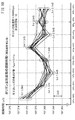
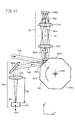
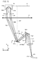
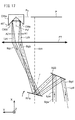
- FIG. 10 is a graph showing a result of actually measuring the reproducibility of the origin signal generated corresponding to each of the reflection surfaces of the polygon mirror by a method as shown in FIGS. 7 and 8 under a predetermined condition different from FIG. It is a figure which shows the structure of the origin sensor by 2nd Embodiment. It is a figure which shows the structure of the origin sensor by 3rd Embodiment. It is the schematic diagram which looked at the structure of FIG. 12 in the surface parallel to XY plane. It is a figure which shows the structure of the origin sensor by 4th Embodiment. It is the figure which showed typically the optical path of each beam of FIG. It is a figure which shows the structure of the origin sensor by 5th Embodiment. It is a figure which shows the modification of a structure of the origin sensor by 5th Embodiment. It is a figure which shows the structure of the origin sensor by 6th Embodiment.
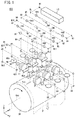
- FIG. 1 is a perspective view showing a schematic configuration of an exposure apparatus (pattern drawing apparatus) EX that performs an exposure process on a substrate (irradiated body) P according to the first embodiment.
- the exposure apparatus EX is a substrate processing apparatus used in a device manufacturing system for manufacturing an electronic device by performing predetermined processing (such as exposure processing) on the substrate P.
- the device manufacturing system is a manufacturing system in which a manufacturing line for manufacturing, for example, a flexible display as an electronic device, a film-like touch panel, a film-like color filter for a liquid crystal display panel, flexible wiring, or a flexible sensor is constructed. System. The following description is based on the assumption that a flexible display is used as the electronic device. Examples of the flexible display include an organic EL display and a liquid crystal display.
- a substrate P is sent from a supply roll (not shown) in which a flexible sheet-like substrate (sheet substrate) P is wound in a roll shape, and various processes are continuously performed on the sent substrate P.
- the substrate P after various treatments is wound up by a collection roll (not shown), which is a so-called roll-to-roll production method. Therefore, the substrate P after various treatments is a multi-sided substrate in which a plurality of devices (display panels) are arranged in a state of being connected in the transport direction of the substrate P.
- the substrate P sent from the supply roll is sequentially subjected to various processes through the process device in the previous process, the exposure apparatus EX, and the process apparatus in the subsequent process, and is taken up by the collection roll.
- the substrate P has a belt-like shape in which the moving direction (transport direction) of the substrate P is the longitudinal direction (long direction) and the width direction is the short direction (short direction).
- a resin film or a foil (foil) made of metal or alloy such as stainless steel is used.
- the material of the resin film include polyethylene resin, polypropylene resin, polyester resin, ethylene vinyl copolymer resin, polyvinyl chloride resin, cellulose resin, polyamide resin, polyimide resin, polycarbonate resin, polystyrene resin, and vinyl acetate resin. Among them, one containing at least one or more may be used.
- the thickness and rigidity (Young's modulus) of the substrate P are within a range in which folds and irreversible wrinkles due to buckling do not occur in the substrate P when passing through the transport path of the device manufacturing system or the exposure apparatus EX. I just need it.
- a film such as PET (polyethylene terephthalate) or PEN (polyethylene naphthalate) having a thickness of about 25 ⁇ m to 200 ⁇ m is typical of a suitable sheet substrate.
- the substrate P may receive heat in each process performed in the device manufacturing system, it is preferable to select the substrate P made of a material whose thermal expansion coefficient is not significantly large.
- the thermal expansion coefficient can be suppressed by mixing an inorganic filler with a resin film.
- the inorganic filler may be, for example, titanium oxide, zinc oxide, alumina, or silicon oxide.
- the substrate P may be a single layer of ultrathin glass having a thickness of about 100 ⁇ m manufactured by a float process or the like, or a laminate in which the above resin film, foil, etc. are bonded to the ultrathin glass. It may be.
- the flexibility of the substrate P means the property that the substrate P can be bent without being sheared or broken even when a force of its own weight is applied to the substrate P. .
- flexibility includes a property of bending by a force of about its own weight.
- the degree of flexibility varies depending on the material, size, and thickness of the substrate P, the layer structure formed on the substrate P, the environment such as temperature or humidity, and the like. In any case, when the substrate P is correctly wound around the various transfer rollers provided in the transfer path in the device manufacturing system (exposure apparatus EX) and the transfer direction changing member such as the rotating drum, the substrate P buckles and the crease is formed. If the substrate P can be smoothly transported without being attached or damaged (breaking or cracking), it can be said to be in the range of flexibility.
- the process device (including a single processing unit or a plurality of processing units) in the preceding process transports the substrate P sent from the supply roll along the longitudinal direction at a predetermined speed toward the exposure apparatus EX. Then, the previous process is performed on the substrate P sent to the exposure apparatus EX.
- the substrate P sent to the exposure apparatus EX by this pre-process is a substrate (photosensitive substrate) having a photosensitive functional layer (photosensitive layer) formed on the surface thereof.
- This photosensitive functional layer is applied as a solution on the substrate P and dried to form a layer (film).
- a typical photosensitive functional layer is a photoresist (in liquid or dry film form), but as a material that does not require development processing, the photosensitivity of the part that has been irradiated with ultraviolet rays is modified.
- SAM silane coupling agent
- a photosensitive reducing agent When a photosensitive silane coupling agent is used as the photosensitive functional layer, the pattern portion exposed to ultraviolet rays on the substrate P is modified from lyophobic to lyophilic.
- a thin film transistor (TFT) or the like can be formed by selectively applying a conductive ink (ink containing conductive nanoparticles such as silver or copper) or a liquid containing a semiconductor material on the lyophilic portion.
- a pattern layer to be an electrode, a semiconductor, insulation, or a wiring for connection can be formed.
- the plating reducing group is exposed to the pattern portion exposed to ultraviolet rays on the substrate P. Therefore, after exposure, the substrate P is immediately immersed in a plating solution containing palladium ions for a certain period of time, so that a pattern layer of palladium is formed (deposited).
- Such a plating process is an additive process, but may be based on an etching process as a subtractive process.
- the substrate P sent to the exposure apparatus EX is made of PET or PEN as a base material, and a metal thin film such as aluminum (Al) or copper (Cu) is vapor-deposited on the entire surface or selectively. It is preferable that a photoresist layer is laminated on the substrate.
- the exposure apparatus (processing apparatus) EX transports the substrate P, which has been transported from the previous process apparatus, to a subsequent process apparatus (including a single processing section or a plurality of processing sections) at a predetermined speed. However, it is a processing apparatus that performs an exposure process on the substrate P.
- the exposure apparatus EX uses light corresponding to a pattern for an electronic device (for example, a pattern of electrodes and wiring of TFTs constituting the electronic device) on the surface of the substrate P (the surface of the photosensitive functional layer, that is, the photosensitive surface). Irradiate the pattern. Thereby, a latent image (modified portion) corresponding to the pattern is formed on the photosensitive functional layer.
- the exposure apparatus EX is a direct drawing type exposure apparatus that does not use a mask as shown in FIG. 1, that is, a so-called spot scanning type exposure apparatus (drawing apparatus).
- the exposure apparatus EX performs pattern exposure for each part of the rotating drum DR that supports the substrate P and conveys it in the longitudinal direction for sub-scanning, and the substrate P that is supported in a cylindrical surface by the rotating drum DR.
- drawing units Un U1 to U6
- each of the plurality of drawing units Un receives spot light SP of a pulsed beam LB (pulse beam) for exposure
- the intensity of the spot light SP is patterned data (drawing data, pattern information) while one-dimensionally scanning (main scanning) with a polygon mirror in a predetermined scanning direction (Y direction) on the irradiated surface (photosensitive surface) of the substrate P.
- modulation ON / OFF
- a light pattern corresponding to a predetermined pattern such as an electronic device, a circuit, or a wiring is drawn and exposed on the irradiated surface of the substrate P.
- the spot light SP is relatively two-dimensionally scanned on the surface to be irradiated (the surface of the photosensitive functional layer) of the substrate P by the sub-scanning of the substrate P and the main scanning of the spot light SP.
- a predetermined pattern is drawn and exposed on the irradiated surface.
- a plurality of exposed areas where the pattern is exposed by the exposure apparatus EX are provided at predetermined intervals along the longitudinal direction of the substrate P. It will be. Since an electronic device is formed in this exposed region, the exposed region is also a device forming region.
- the rotary drum DR has a central axis AXo extending in the Y direction and extending in a direction intersecting with the direction in which gravity works, and a cylindrical outer peripheral surface having a constant radius from the central axis AXo.
- the rotating drum DR rotates around the central axis AXo while supporting (holding) a part of the substrate P by bending the outer surface (circumferential surface) into a cylindrical surface in the longitudinal direction. P is transported in the longitudinal direction.
- the rotating drum DR supports an area (part) on the substrate P onto which the beam LB (spot light SP) from each of the plurality of drawing units Un (U1 to U6) is projected on its outer peripheral surface.
- the rotating drum DR supports (holds and holds) the substrate P from the surface (back surface) opposite to the surface on which the electronic device is formed (surface on which the photosensitive surface is formed).
- shafts (not shown) supported by bearings are provided so as to rotate the rotating drum DR around the central axis AXo.
- the shaft is given a rotational torque from a rotational drive source (not shown) (for example, a motor or a speed reduction mechanism), and the rotary drum DR rotates around the central axis AXo at a constant rotational speed.
- the light source device LS generates and emits a pulsed beam (pulse beam, pulsed light, laser) LB.
- This beam LB is ultraviolet light having sensitivity to the photosensitive layer of the substrate P and having a peak wavelength in a wavelength band of 370 nm or less.
- the light source device LS emits and emits a pulsed beam LB at a frequency (oscillation frequency, predetermined frequency) Fa according to control of a drawing control device (not shown).
- the light source device LS includes a semiconductor laser element that generates pulsed light in the infrared wavelength range, a fiber amplifier, and a wavelength conversion element (harmonic) that converts the amplified pulsed light in the infrared wavelength range into pulsed light in the ultraviolet wavelength range.
- a fiber amplifier laser light source including a wave generating element By configuring the light source device LS in this manner, high-intensity ultraviolet pulsed light having an oscillation frequency Fa of several hundred MHz and a light emission time of one pulse of several tens of picoseconds or less is obtained. It is assumed that the beam LB emitted from the light source device LS is a thin parallel light beam having a beam diameter of about 1 mm or less. For the configuration in which the light source device LS is a fiber amplifier laser light source and the pulse generation of the beam LB is turned on / off at high speed according to the state of the pixels constituting the drawing data (logical value “0” or “1”). This is disclosed in the pamphlet of published No. 2015/166910.
- a beam LB emitted from the light source device LS includes a selection optical element OSn (OS1 to OS6) as a plurality of switching elements, a plurality of reflection mirrors M1 to M12, a plurality of incident mirrors IMn (IM1 to IM6), The light is selectively (alternatively) supplied to each of the drawing units Un (U1 to U6) via a beam switching unit including an absorber TR and the like.
- the selection optical elements OSn (OS1 to OS6) are transmissive to the beam LB, and are driven by an ultrasonic signal to deflect and emit the first-order diffracted light of the incident beam LB at a predetermined angle.
- An acousto-optic modulator (AOM: Acousto-Optic Modulator).
- the plurality of selection optical elements OSn and the plurality of incident mirrors IMn are provided corresponding to each of the plurality of drawing units Un.
- the selection optical element OS1 and the incident mirror IM1 are provided corresponding to the drawing unit U1
- the selection optical element OS2 to OS6 and the incidence mirror IM2 to IM6 correspond to the drawing units U2 to U6, respectively. Is provided.
- the beam LB from the light source device LS is guided to the absorber TR by the reflection mirrors M1 to M12 having its optical path bent in a spiral shape.
- OSn selection optical elements
- OS6 selection optical elements
- an off state a state where no ultrasonic signal is applied and no first-order diffracted light is generated
- a plurality of lenses are provided in the beam optical path from the reflection mirror M1 to the absorber TR, and the plurality of lenses converge the beam LB from the parallel light flux or after convergence.
- the diverging beam LB is returned to a parallel light beam. The configuration will be described later with reference to FIG.
- the beam LB from the light source device LS travels in the ⁇ X direction parallel to the X axis and enters the reflection mirror M1.
- the beam LB reflected in the ⁇ Y direction by the reflection mirror M1 enters the reflection mirror M2.
- the beam LB reflected in the + X direction by the reflection mirror M2 passes straight through the selection optical element OS5 and reaches the reflection mirror M3.
- the beam LB reflected in the ⁇ Y direction by the reflection mirror M3 enters the reflection mirror M4.
- the beam LB reflected in the ⁇ X direction by the reflection mirror M4 passes straight through the selection optical element OS6 and reaches the reflection mirror M5.
- the beam LB reflected in the ⁇ Y direction by the reflection mirror M5 enters the reflection mirror M6.
- the beam LB reflected in the + X direction by the reflection mirror M6 passes straight through the selection optical element OS3 and reaches the reflection mirror M7.
- the beam LB reflected in the ⁇ Y direction by the reflection mirror M7 enters the reflection mirror M8.
- the beam LB reflected in the ⁇ X direction by the reflection mirror M8 passes straight through the selection optical element OS4 and reaches the reflection mirror M9.
- the beam LB reflected in the ⁇ Y direction by the reflection mirror M9 enters the reflection mirror M10.
- the beam LB reflected in the + X direction by the reflection mirror M10 passes straight through the selection optical element OS1 and reaches the reflection mirror M11.
- the beam LB reflected in the ⁇ Y direction by the reflection mirror M11 enters the reflection mirror M12.
- the beam LB reflected in the ⁇ X direction by the reflection mirror M12 passes straight through the selection optical element OS2 and is guided to the absorber TR.
- the absorber TR is an optical trap that absorbs the beam LB in order to suppress leakage of the beam LB to the outside.
- each of the selection optical elements OSn (OS1 to OS6) has a function of deflecting the optical path of the beam LB from the light source device LS.
- the beam LBn (LB1 to LB6) deflected by each of the selection optical elements OSn is the original. It is lower than the intensity of the beam LB.
- the drawing control device controls the selected optical element OSn (OS1 to OS6) so that only one of the selected optical elements OSn (OS1 to OS6) is turned on for a predetermined time.
- one selected optical element OSn is in the ON state, about 20% of zero-order light that travels straight without being diffracted by the optical element for selection OSn remains, but it is finally absorbed by the absorber TR.
- Each of the selection optical elements OSn is installed so as to deflect the beam LBn (LB1 to LB6) which is the deflected first-order diffracted light in the ⁇ Z direction with respect to the incident beam LB.
- Beams LBn (LB1 to LB6) deflected and emitted from each of the selection optical elements OSn are projected onto incident mirrors IMn (IM1 to IM6) provided at positions away from each of the selection optical elements OSn by a predetermined distance. Is done.
- Each incident mirror IMn reflects the incident beam LBn (LB1 to LB6) in the ⁇ Z direction, thereby guiding the beam LBn (LB1 to LB6) to the corresponding drawing unit Un (U1 to U6).
- each selection optical element OSn may be used.
- Each of the plurality of optical elements for selection OSn turns on / off generation of diffracted light obtained by diffracting the incident beam LB in accordance with on / off of a drive signal (ultrasonic signal) from the drawing control device.
- the selection optical element OS5 transmits the incident beam LB from the light source device LS without diffracting it when the drive signal (high frequency signal) from the drawing control device is not applied and is in the off state. Therefore, the beam LB transmitted through the selection optical element OS5 enters the reflection mirror M3.
- the selection optical element OS5 is in the on state, the incident beam LB is diffracted and directed to the incident mirror IM5.
- the switching (beam selection) operation by the selection optical element OS5 is controlled by turning on / off the drive signal.
- the switching operation of each selection optical element OSn can guide the beam LB from the light source device LS to any one drawing unit Un, and switch the drawing unit Un on which the beam LBn is incident. Can do.
- a configuration in which a plurality of selection optical elements OSn are sequentially arranged in series with respect to the beam LB from the light source device LS and the beam LBn is supplied to the corresponding drawing unit Un in a time-sharing manner.
- each of the selection optical elements OSn (OS1 to OS6) constituting the beam switching unit is turned on for a predetermined time is, for example, OS1 ⁇ OS2 ⁇ OS3 ⁇ OS4 ⁇ OS5 ⁇ OS6 ⁇ OS1 ⁇ .
- This order is determined by the order of the scanning start timing by the spot light set in each of the drawing units Un (U1 to U6). That is, in the present embodiment, any one of the drawing units U1 to U6 is synchronized with the rotation speed of the polygon mirror provided in each of the six drawing units U1 to U6 in synchronization with the phase of the rotation angle. It is possible to switch to the time division so that one reflection surface of the polygon mirror in one of them performs one spot scanning on the substrate P.
- the order of spot scanning of the drawing unit Un may be any as long as the phase of the rotation angle of each polygon mirror of the drawing unit Un is synchronized in a predetermined relationship.
- three drawing units U1, U3, U5 are arranged in the Y direction on the upstream side in the transport direction of the substrate P (the direction in which the outer peripheral surface of the rotary drum DR moves in the circumferential direction).
- Three drawing units U2, U4, U6 are arranged in the Y direction on the downstream side in the transport direction.
- pattern drawing on the substrate P is started from the upstream odd-numbered drawing units U1, U3, U5, and when the substrate P is fed for a certain length, the even-numbered drawing units U2, U4, U6 on the downstream side. Since pattern drawing is also started, the order of spot scanning of the drawing unit Un can be set as U1 ⁇ U3 ⁇ U5 ⁇ U2 ⁇ U4 ⁇ U6 ⁇ U1 ⁇ . Therefore, the order in which each of the selection optical elements OSn (OS1 to OS6) is turned on for a predetermined time is determined as OS1 ⁇ OS3 ⁇ OS5 ⁇ OS2 ⁇ OS4 ⁇ OS6 ⁇ OS1 ⁇ .
- the on / off switching control of the selection optical element OSn is performed based on the drawing data. By doing so, the spot is forcibly maintained in the off state, so spot scanning by the drawing unit Un is not performed.
- each of the drawing units U1 to U6 is provided with a polygon mirror (scanning member) PM for main scanning the incident beams LB1 to LB6.
- the polygon mirrors PM of the respective drawing units Un are synchronously controlled so as to maintain a constant rotational angle phase with each other while precisely rotating at the same rotational speed.
- the main scanning timing (main scanning period of the spot light SP) of each of the beams LB1 to LB6 projected onto the substrate P from each of the drawing units U1 to U6 can be set so as not to overlap each other.
- each of the selection optical elements OSn (OS1 to OS6) provided in the beam switching unit is controlled in synchronization with the rotation angle positions of the six polygon mirrors PM, thereby providing a light source.
- An efficient exposure process can be performed in which the beam LB from the apparatus LS is distributed in time division to each of the plurality of drawing units Un.
- the exposure apparatus EX is a so-called multi-head type direct drawing exposure system in which a plurality of drawing units Un (U1 to U6) having the same configuration are arranged.
- Each of the drawing units Un draws a pattern for each partial region partitioned in the Y direction of the substrate P supported by the outer peripheral surface (circumferential surface) of the rotary drum DR.
- Each drawing unit Un (U1 to U6) condenses (converges) the beam LBn on the substrate P while projecting the beam LBn from the beam switching unit onto the substrate P (on the irradiated surface of the substrate P). Thereby, the beam LBn (LB1 to LB6) projected onto the substrate P becomes the spot light SP.
- the spot light SP of the beam LBn (LB1 to LB6) projected on the substrate P is scanned in the main scanning direction (Y direction) by the rotation of the polygon mirror PM of each drawing unit Un.
- the drawing line SLn is also a scanning locus on the substrate P of the spot light SP of the beam LBn.
- the drawing unit U1 scans the spot light SP along the drawing line SL1, and similarly, the drawing units U2 to U6 scan the spot light SP along the drawing lines SL2 to SL6.
- the drawing lines SLn (SL1 to SL6) of the plurality of drawing units Un (U1 to U6) include a central plane that includes the central axis AXo of the rotary drum DR and is parallel to the YZ plane. It is arranged in a staggered arrangement in two rows in the circumferential direction of DR.
- the odd-numbered drawing lines SL1, SL3, SL5 are located on the irradiated surface of the substrate P on the upstream side ( ⁇ X direction side) in the transport direction of the substrate P with respect to the center surface, and along the Y direction. They are arranged in a row at a predetermined interval.
- the even-numbered drawing lines SL2, SL4, SL6 are located on the irradiated surface of the substrate P on the downstream side (+ X direction side) in the transport direction of the substrate P with respect to the center surface, and are predetermined along the Y direction. Are arranged in a row separated by an interval of.
- a plurality of drawing units Un (U1 to U6) are also arranged in a staggered arrangement in two rows in the transport direction of the substrate P across the center plane, and odd-numbered drawing units U1, U3, U5 and even-numbered drawing
- the units U2, U4, and U6 are provided symmetrically with respect to the center plane when viewed in the XZ plane.
- the odd-numbered drawing lines SL1, SL3, SL5 and the even-numbered drawing lines SL2, SL4, SL6 are separated from each other, but the Y direction (the width direction of the substrate P).
- the main scanning direction) is set to be joined without being separated from each other.
- the drawing lines SL1 to SL6 are substantially parallel to the width direction of the substrate P, that is, the central axis AXo of the rotary drum DR.
- joining the drawing lines SLn in the Y direction means that the positions of the ends of the drawing lines SLn are adjacent or partially overlapped.
- the length of each drawing line SLn may be overlapped within a range of several percent or less in the Y direction including the drawing start point or the drawing end point. .
- the plurality of drawing units Un share the Y-direction scanning area (the main scanning range section) so as to cover the width dimension of the exposure area on the substrate P in total. ing.
- the main scanning range in the Y direction the length of the drawing line SLn
- drawing can be performed by arranging a total of six drawing units U1 to U6 in the Y direction.
- the width in the Y direction of a large exposure area is increased to about 180 to 360 mm.
- the length of each drawing line SLn (SL1 to SL6) (length of the drawing range) is basically the same. That is, the scanning distance of the spot light SP of the beam LBn scanned along each of the drawing lines SL1 to SL6 is basically the same.
- the spot light SP projected on the drawing line SLn during the main scanning is the beam LB. It becomes discrete according to the oscillation frequency Fa (for example, 400 MHz). Therefore, it is necessary to overlap the spot light SP projected by one pulse light of the beam LB and the spot light SP projected by the next one pulse light in the main scanning direction.
- the amount of overlap is set by the size ⁇ of the spot light SP, the scanning speed (main scanning speed) Vs of the spot light SP, and the oscillation frequency Fa of the beam LB.
- the effective size (diameter) ⁇ of the spot light SP is 1 / e 2 (or 1/2) of the peak intensity of the spot light SP when the intensity distribution of the spot light SP is approximated by a Gaussian distribution. Determined by width dimension.
- the scanning speed Vs of the spot light SP rotational speed of the polygon mirror PM
- the spot light SP so that the spot light SP overlaps the effective size (dimension) ⁇ by about ⁇ ⁇ 1 ⁇ 2.
- the oscillation frequency Fa is set. Therefore, the projection interval along the main scanning direction of the pulsed spot light SP is ⁇ / 2.
- the substrate P is effective for the spot light SP between one scanning of the spot light SP along the drawing line SLn and the next scanning. It is desirable to set so as to move by a distance of about 1 ⁇ 2 of a large size ⁇ . Further, when drawing lines SLn adjacent in the Y direction are continued in the main scanning direction, it is desirable to overlap by ⁇ / 2. In the present embodiment, the size (dimension) ⁇ of the spot light SP is set to about 3 to 4 ⁇ m.
- Each drawing unit Un (U1 to U6) is set so that each beam LBn travels toward the central axis AXo of the rotary drum DR when viewed in the XZ plane.
- the optical path (beam principal ray) of the beam LBn traveling from each drawing unit Un (U1 to U6) toward the substrate P becomes parallel to the normal line of the irradiated surface of the substrate P in the XZ plane.
- the beam LBn irradiated from each of the drawing units Un (U1 to U6) to the drawing line SLn (SL1 to SL6) is relative to the tangential plane at the drawing line SLn on the surface of the substrate P curved into a cylindrical surface. It is projected toward the substrate P so as to be always vertical. That is, with respect to the main scanning direction of the spot light SP, the beams LBn (LB1 to LB6) projected onto the substrate P are scanned in a telecentric state.
- the drawing unit U1 includes at least reflecting mirrors M20 to M24, a polygon mirror PM, and an f ⁇ lens system (drawing scanning lens) FT.
- the first cylindrical lens CYa (see FIG. 2) is disposed in front of the polygon mirror PM when viewed from the traveling direction of the beam LB1, and the second cylindrical lens FT is behind the f ⁇ lens system FT.
- the cylindrical lens CYb (see FIG. 2) is provided.
- the first cylindrical lens CYa and the second cylindrical lens CYb correct the position variation in the sub-scanning direction of the spot light SP (drawing line SL1) due to the tilt error of each reflecting surface of the polygon mirror PM.
- the beam LB1 reflected in the ⁇ Z direction by the incident mirror IM1 enters the reflection mirror M20 provided in the drawing unit U1, and the beam LB1 reflected by the reflection mirror M20 advances in the ⁇ X direction and enters the reflection mirror M21.
- the beam LB1 reflected in the ⁇ Z direction by the reflection mirror M21 enters the reflection mirror M22, and the beam LB1 reflected by the reflection mirror M22 advances in the + X direction and enters the reflection mirror M23.
- the reflection mirror M23 reflects the incident beam LB1 toward the reflection surface RP of the polygon mirror PM so as to be bent in a plane parallel to the XY plane.
- the polygon mirror PM reflects the incident beam LB1 toward the + ⁇ direction toward the f ⁇ lens system FT.
- the polygon mirror PM deflects (reflects) the incident beam LB1 one-dimensionally in a plane parallel to the XY plane in order to scan the spot light SP of the beam LB1 on the irradiated surface of the substrate P.
- the polygon mirror (rotating polygonal mirror, movable deflecting member) PM includes a rotating shaft AXp extending in the Z-axis direction and a plurality of reflecting surfaces RP (reflecting in the present embodiment) formed around the rotating shaft AXp.
- the number of planes RP is assumed to be 8).
- the reflection angle of the pulsed beam LB1 irradiated on the reflection surface can be continuously changed by rotating the polygon mirror PM around the rotation axis AXp in a predetermined rotation direction.
- the beam LB1 is deflected by one reflecting surface RP, and the spot light SP of the beam LB1 irradiated on the irradiated surface of the substrate P is scanned along the main scanning direction (the width direction of the substrate P, the Y direction). can do.
- the number of drawing lines SL1 in which the spot light SP is scanned on the irradiated surface of the substrate P by one rotation of the polygon mirror PM is eight, which is the same as the number of the reflecting surfaces RP.
- the f ⁇ lens system (scanning lens, scanning optical system) FT is a telecentric scanning lens that projects the beam LB1 reflected by the polygon mirror PM onto the reflecting mirror M24.
- the beam LB1 transmitted through the f ⁇ lens system FT is projected onto the substrate P as the spot light SP through the reflection mirror M24.
- the reflection mirror M24 reflects the beam LB1 toward the substrate P so that the beam LB1 travels toward the central axis AXo of the rotary drum DR with respect to the XZ plane.
- the incident angle ⁇ of the beam LB1 to the f ⁇ lens system FT varies depending on the rotation angle ( ⁇ / 2) of the polygon mirror PM.
- the f ⁇ lens system FT projects the beam LB1 to the image height position on the irradiated surface of the substrate P in proportion to the incident angle ⁇ through the reflection mirror M24.
- the focal length of the f ⁇ lens system FT is fo and the image height position is yo
- the surface (parallel to the XY plane) on which the beam LB1 incident on the f ⁇ lens system FT is deflected one-dimensionally by the polygon mirror PM is a surface including the optical axis AXf of the f ⁇ lens system FT.
- the optical configuration of the drawing unit Un (U1 to U6) will be described with reference to FIGS.
- the drawing unit Un along the traveling direction of the beam LBn from the incident position of the beam LBn to the irradiated surface (substrate P), the reflection mirror M20, the reflection mirror M20a, and the polarization beam splitter BSd.
- the drawing unit Un in order to detect the drawing start possible timing of the drawing unit Un (scanning start timing of the spot light SP), as shown in FIG. 3, the angular position of each reflecting surface of the polygon mirror PM is set.
- a beam transmitter 60a and a beam receiver 60b photoelectric detector
- the configuration of the origin sensor (the beam transmitter 60a and the beam receiver 60b) will be described in detail later.
- the reflected light of the beam LBn reflected by the irradiated surface of the substrate P (or the surface of the rotating drum DR) is converted into the f ⁇ lens system FT, the polygon mirror PM, the polarization beam splitter BSd, and the like.
- a photodetector DTc is provided for detection via
- the beam LBn incident on the drawing unit Un travels in the ⁇ Z direction along the optical axis AX1 parallel to the Z axis, and is incident on the reflection mirror M20 inclined by 45 ° with respect to the XY plane.
- the beam LBn reflected by the reflection mirror M20 travels in the ⁇ X direction toward the reflection mirror M20a that is separated from the reflection mirror M20 in the ⁇ X direction.
- the reflection mirror M20a is disposed with an inclination of 45 ° with respect to the YZ plane, and reflects the incident beam LBn toward the polarization beam splitter BSd in the ⁇ Y direction.
- the polarization separation surface of the polarization beam splitter BSd is disposed at an angle of 45 ° with respect to the YZ plane, reflects a P-polarized beam, and transmits a linearly polarized (S-polarized) beam polarized in a direction orthogonal to the P-polarized light. If the beam LBn incident on the drawing unit Un is a P-polarized beam, the polarization beam splitter BSd reflects the beam LBn from the reflection mirror M20a in the ⁇ X direction and guides it to the reflection mirror M21 side.
- the reflection mirror M21 is disposed at an angle of 45 ° with respect to the XY plane, and reflects the incident beam LBn in the ⁇ Z direction toward the reflection mirror M22 that is separated from the reflection mirror M21 in the ⁇ Z direction.
- the beam LBn reflected by the reflection mirror M21 enters the reflection mirror M22.
- the reflection mirror M22 is disposed with an inclination of 45 ° with respect to the XY plane, and reflects the incident beam LBn toward the reflection mirror M23 in the + X direction.
- the beam LBn reflected by the reflection mirror M22 enters the reflection mirror M23 via a ⁇ / 4 wavelength plate (not shown) and a cylindrical lens CYa.
- the reflection mirror M23 reflects the incident beam LBn toward the polygon mirror PM.
- the polygon mirror PM reflects the incident beam LBn toward the + X direction toward an f ⁇ lens system FT having an optical axis AXf parallel to the X axis.
- the polygon mirror PM deflects (reflects) the incident beam LBn one-dimensionally in a plane parallel to the XY plane in order to scan the spot light SP of the beam LBn on the irradiated surface of the substrate P.
- the polygon mirror PM has a plurality of reflecting surfaces (each side of a regular octagon in this embodiment) formed around a rotation axis AXp extending in the Z-axis direction, and is rotated by a rotation motor RM coaxial with the rotation axis AXp. Is done.
- the rotation motor RM is rotated at a constant rotation speed (for example, about 30,000 to 40,000 rpm) by a drawing control device (not shown).
- the effective length (for example, 50 mm) of the drawing lines SLn is the maximum scanning length (for example, 52 mm) at which the spot light SP can be scanned by the polygon mirror PM.
- the length is set as follows, and in the initial setting (design), the center point of the drawing line SLn (the point through which the optical axis AXf of the f ⁇ lens system FT passes) is set at the center of the maximum scanning length.
- the cylindrical lens CYa converges the incident beam LBn on the reflection surface of the polygon mirror PM in the sub-scanning direction (Z direction) orthogonal to the main scanning direction (rotation direction) of the polygon mirror PM. That is, the cylindrical lens CYa converges the beam LBn in a slit shape (ellipse shape) extending in a direction parallel to the XY plane on the reflection surface of the polygon mirror PM. Even when the reflection surface of the polygon mirror PM is tilted from a state parallel to the Z axis by a cylindrical lens CYa whose generating line is parallel to the Y direction and a cylindrical lens CYb described later, the substrate P is irradiated. It is possible to prevent the irradiation position of the beam LBn (drawing line SLn) irradiated on the surface from shifting in the sub-scanning direction.
- a slit shape ellipse shape
- the incident angle ⁇ of the beam LBn to the f ⁇ lens system FT (the angle with respect to the optical axis AXf) varies depending on the rotation angle ( ⁇ / 2) of the polygon mirror PM.
- the incident angle ⁇ of the beam LBn to the f ⁇ lens system FT is 0 degree
- the beam LBn incident on the f ⁇ lens system FT advances along the optical axis AXf.
- the beam LBn from the f ⁇ lens system FT is reflected in the ⁇ Z direction by the reflecting mirror M24, and is projected toward the substrate P through the cylindrical lens CYb.
- the beam LBn projected onto the substrate P by the f ⁇ lens system FT and the cylindrical lens CYb whose generating line is parallel to the Y direction is a minute spot light having a diameter of about several ⁇ m (for example, 3 to 4 ⁇ m) on the irradiated surface of the substrate P. Converged to SP.
- the beam LBn incident on the drawing unit Un is bent along the optical path cranked in a U-shape from the reflection mirror M20 to the substrate P when viewed in the XZ plane, and proceeds in the ⁇ Z direction to the substrate. Projected to P.
- Each of the six drawing units U1 to U6 scans the spot light SP of the beams LB1 to LB6 one-dimensionally in the main scanning direction (Y direction) and conveys the substrate P in the longitudinal direction, thereby The irradiated surface is relatively two-dimensionally scanned by the spot light SP, and the pattern drawn on each of the drawing lines SL1 to SL6 is exposed on the substrate P in a state where the patterns are joined in the Y direction.
- the effective scanning length LT of the drawing lines SLn is 50 mm
- the effective diameter ⁇ of the spot light SP is 4 ⁇ m
- the oscillation frequency Fa of the pulse emission of the beam LB from the light source device LS is 400 MHz.
- the pulsed light is emitted so that the spot light SP overlaps by 1/2 of the diameter ⁇ along the drawing line SLn (main scanning direction)
- the pixel size Pxy defined on the drawing data is set to 4 ⁇ m square on the substrate P, and one pixel is exposed by two pulses of the spot light SP in each of the main scanning direction and the sub-scanning direction.
- the scanning speed Vsp becomes high, it is also necessary to improve the reproducibility of the generation timing of the origin signal from the origin sensor (the beam transmitter 60a and the beam receiver 60b) that determines the pattern drawing start timing.
- the minimum dimension (minimum line width) of a pattern to be drawn is 8 ⁇ m (for two pixels)
- a new pattern is superimposed on the pattern already formed on the substrate P and exposed.
- the overlay accuracy (allowable position error range) in the second exposure is required to be about 1 ⁇ 4 to 5 of the minimum line width. That is, when the minimum line width is 8 ⁇ m, the allowable position error range is 2 ⁇ m to 1.6 ⁇ m.
- This value is equal to or less than the interval of two pulses of the spot light SP corresponding to the oscillation period Tf (2.5 nS) of the beam LB from the light source device LS, and it is confirmed that an error for one pulse of the spot light SP is not allowed. means. For this reason, the reproducibility of the origin signal generation timing that determines the pattern drawing start timing (start position) needs to be set to a period Tf (2.5 nS) or less.
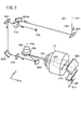
- FIG. 3 shows a plane parallel to the XY plane in which the polygon mirror PM, the optical axis AXf of the f ⁇ lens system FT, the beam transmitting unit 60a constituting the origin sensor, the beam receiving unit 60b, and the like are arranged in the drawing unit Un. It is the figure seen inside.
- a drawing beam LBn is projected toward one of the reflecting surfaces RPa of the reflecting surface RP of the polygon mirror PM, and is reflected next to the reflecting surface RPa of the polygon mirror PM (one before).
- a laser beam (origin detection beam, detection beam) Bga from the beam transmitter 60a is projected onto the surface RPb. Further, the angular position of the reflection surface RPa in FIG.
- the reflection surface RP (RPa) of the polygon mirror PM is disposed so as to be positioned on the entrance pupil plane orthogonal to the optical axis AXf of the f ⁇ lens system FT.
- the beam LBn traveling from the reflecting mirror M23 toward the polygon mirror PM A reflection surface RP (RPa) is set at a position where the principal ray and the optical axis AXf intersect.
- the distance from the main surface of the f ⁇ lens system FT to the surface of the substrate P (the condensing point of the spot light SP) is the focal length fo.
- the laser beam Bga from the beam transmitting unit 60a is projected onto the reflecting surface RPb of the polygon mirror PM as a parallel light flux in a non-photosensitive wavelength range with respect to the photosensitive functional layer of the substrate P.
- the reflected beam Bgb of the laser beam Bga reflected by the reflecting surface RPb is directed to the reflecting mirror (beam reflecting portion) MRa having a reflecting surface perpendicular to the XY plane.
- the reflected beam Bgc of the beam Bgb reflected by the reflecting mirror MRa is again projected toward the reflecting surface RPb of the polygon mirror PM.
- the reflected beam Bgd of the beam Bgc reflected by the reflecting surface RPb is received by the beam receiving unit 60b. As shown in FIG.
- the beam receiving unit 60 b is as shown in FIG. 3 at the moment when the reflecting surface RPb (and each other reflecting surface RP) of the polygon mirror PM is at a specific angular position in a plane (XY plane) parallel to the XY plane.
- the beams Bga, Bgb, Bgc, and Bgd travel, and the beam receiving unit 60b outputs an origin signal SZn that changes in waveform in a pulse shape.
- the beam Bga is shown as a simple line.
- the beam transmission unit 60 a has a parallel light flux having a predetermined width with respect to the rotation direction of the reflection surface RP of the polygon mirror PM in the XY plane.
- the beam Bgd is shown as a simple line, but actually, the beam Bgd becomes a parallel light beam having a predetermined width in the XY plane, and the beam Bgd is directed to the beam receiving unit 60b according to the rotation of the polygon mirror PM.
- the beam receiving unit 60b includes a photoelectric conversion element that outputs an origin signal SZn when receiving the beam Bgd, and a condensing lens that collects the beam Bgd as a spot on the light receiving surface of the photoelectric conversion element.
- FIG. 4 shows a detailed configuration of the photoelectric conversion element (photoelectric detector) DTo provided in the beam receiving unit 60b.
- the photoelectric conversion element photoelectric detector
- the photo IC includes light receiving surfaces PD1 and PD2 formed by two PIN photodiodes arranged with a narrow gap (dead zone) in the scanning direction of the spot light SPr of the beam Bgd collected by the condenser lens.
- the current amplification units IC1 and IC2 and the comparator unit IC3 are packaged into one.
- the spot light SPr crosses in the order of the light receiving surfaces PD1 and PD2, and each of the current amplifying parts IC1 and IC2 is as shown in FIG.
- Output signals STa and STb are generated.
- a constant offset voltage (reference voltage) Vref is applied to the current amplification unit IC1 that amplifies the photocurrent from the light receiving surface PD1 that first receives the spot light SPr, and the output signal STa of the current amplification unit IC1 is received by the light receiving surface PD1. Is biased so as to be at the reference voltage Vref when the photocurrent generated at is zero.
- the comparator IC3 compares the levels of the output signals STa and STb.
- the comparator unit IC3 When the STa> STb, the comparator unit IC3 outputs a logic signal that is at the H level, and when STa ⁇ STb, the L level. Output as signal SZn.
- the time point when the origin signal SZn transitions from the H level to the L level is defined as the origin time (origin position) Tog, and the generation timing of the origin signal SZn means the origin time Tog.
- the origin position is, for example, when the point on the substrate P through which the optical axis AXf of the f ⁇ lens system FT passes is used as a reference point, the main scanning direction of the spot light SP from the reference point Does not mean the origin as an absolute position that is always set a certain distance before, but relatively represents a predetermined distance before (or a predetermined time before) the pattern drawing start timing along the drawing line SLn. Is.
- the origin time Tog is the moment when the levels of the output signals STa and STb coincide with each other while the level of the output signal STb rises while the level of the output signal STa falls.
- the level changes (rise and fall waveforms) of the output signals STa and STb are caused by the relationship between the width dimension of the light receiving surfaces PD1 and PD2 and the size of the spot light SPr, the scanning speed Vh of the spot light SPr and the response of the light receiving surfaces PD1 and PD2.
- the diameter of the spot light SPr is larger than the width of the dead zone and smaller than the width of the light receiving surface PD1
- each of the output signals STa and STb is as shown in FIG.
- a waveform is generated by the level change, and a stable origin signal SZn is obtained.
- the spot B of the beam Bgd after the beam Bga for detecting the origin is reflected twice by the reflecting surface RP (RPb) of the polygon mirror PM using the reflecting mirror MRa.
- the optical SPr is configured to receive light by the photoelectric conversion element DTo. Therefore, the scanning speed Vh of the spot light SPr on the light receiving surfaces PD1 and PD2 is obtained when the origin detection beam Bga is reflected once by the reflection surface RP (RPb) of the polygon mirror PM and received by the photoelectric conversion element DTo. Can be doubled or more.
- the scanning of the beam Bgd (spot light SPr) for detecting the origin on the photoelectric conversion element DTo is compared with the scanning speed Vsp of the drawing beam LBn (spot light SP) on the substrate P.
- the speed Vh can be increased by about twice, and the reproducibility of the generation timing of the origin signal SZn can be improved (the 3 ⁇ value representing the variation distribution width is reduced).
- the configuration is such that the reflected beam Bgb obtained by reflecting the origin detecting beam Bga once by the reflecting surface RP (RPb) of the polygon mirror PM is received by the photoelectric conversion element DTo of the beam receiving unit 60b.
- the spot light is compared with the scanning speed Vsp of the spot light SP.
- the reproducibility of the origin signal SZn is compared with the case where the SPr scanning speed Vh is increased to about twice.
- a beam transmitter 60a includes a semiconductor laser light source LDo that continuously emits a laser beam Bga, a collimator lens GLa (first optical element having a refractive power) that converts the beam Bga from the light source into a parallel light beam, and the like.
- the beam Bga is a parallel light beam having a certain width with respect to the rotation direction of the reflection surface RP (RPb) (main scanning direction parallel to the XY plane).
- the reflected light beam Bgb is focused on the spot light SPr narrowed down in the main scanning direction on the same photoelectric conversion element DTo as in FIG. 2 optical elements).
- the light receiving surfaces PD1 and PD2 of the photoelectric conversion element DTo shown in FIG. 4 are arranged at the focal length Fgs on the rear side of the lens system GLb.
- the spot light SPr of the reflected beam Bgb is approximately at the center of the light receiving surface of the photoelectric conversion element DTo (light receiving surfaces PD1, PD2). It is set to be located in the dead zone).
- the beam receiving unit 60b forms a detection unit for generating the origin signal SZn by the photoelectric conversion element DTo and the lens system GLb.
- the reflected beam Bgb ′ is in the same plane as the light receiving surface of the photoelectric conversion element DTo. It is condensed.
- the reflected beam Bgb ′ from the lens system GLb toward the photoelectric conversion element DTo does not have to be telecentric.
- the focal length Fgs of the lens system GLb is set to about twice the focal length fo of the f ⁇ lens system FT
- the scanning speed Vh can be increased by about twice.
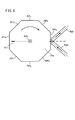
- FIG. 6 is a plan view of the eight-sided polygon mirror PM shown in FIGS. 1 to 3.
- the origin signal SZn generated as shown in FIG. 4B is shown.
- the eight reflecting surfaces RP are set to RPa, RPb, RPc, RPd, RPe, RPf, RPg, and RPh in the direction opposite to the rotation direction (clockwise) of the polygon mirror PM.
- a rotation reference mark Mcc for detecting the origin of rotation of the polygon mirror PM is formed on the upper surface (or lower surface) of the polygon mirror PM.
- the rotation reference mark Mcc is detected by a reflective photoelectric sensor (also referred to as a rotation detection sensor) that outputs a pulsed detection signal each time the polygon mirror PM rotates once.
- the speed fluctuation of the polygon mirror PM is measured based on the origin signal SZn.
- the servo control is performed by the drawing control device so that the motor RM of the polygon mirror PM is rotated at 36000 rpm, the polygon mirror PM will be rotated 600 times per second, which is one design rotation.
- the lap time TD for 1 minute is 1/600 second ( ⁇ 166.667 ⁇ S).
- the actual circulation time TD from the origin time Tog of any one pulse in the origin signal SZn to the origin time Tog of the ninth pulse is set to be smaller than the oscillation frequency Fa used by the light source device LS for pulse emission. Measure repeatedly using high frequency clock pulses. Since the polygon mirror PM rotates at high speed with inertia, the possibility of uneven speed during one rotation is low. TD may fluctuate slightly.
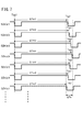
- FIG. 7 is a diagram for explaining a method of measuring the reproducibility (variation) of the generation timing of the origin signal SZn.
- an example of how to obtain the reproducibility of the origin time Tog2 of the origin signal SZn generated corresponding to the reflection surface RPa of the polygon mirror PM shown in FIG. The same measurement can be performed for each of RPb to RPh.
- the origin time Tog1 generated at the timing just before the origin time Tog2 is obtained as the origin signal SZn generated corresponding to the reflection surface RPh of the polygon mirror PM.
- the waveforms of the origin signals SZn (a) 1 to SZn (a) 7 generated while the polygon mirror PM rotates 7 times are obtained corresponding to the reflecting surface RPh.
- the origin times Tog1 are aligned and shown on the time axis.
- the measured values of the origin interval time ⁇ Tmn which should be constant, vary. Since this variation becomes a variation width ⁇ Te of the generation timing of the origin time Tog2 corresponding to the reflection surface RPa, the reproducibility of the origin signal SZn is a standard deviation value ⁇ of a large number of origin times Tog2 distributed within the variation width ⁇ Te. Alternatively, it is obtained as a 3 ⁇ value that is three times the standard deviation value ⁇ . As described above, when the light source device LS oscillates the beam LB with the period Tf, the 3 ⁇ value as reproducibility is preferably smaller than the period Tf.
- FIG. 8 is a diagram schematically showing a method for predicting a time error due to speed fluctuation of the polygon mirror PM.
- the origin interval time ⁇ Tmn corresponding to each of the eight reflecting surfaces RPa to RPh is measured for every number of rounds of the polygon mirror PM.
- the initial position (first origin time Tog) during one rotation of the polygon mirror PM is the reflection surface RPa, and the waveform of the origin signal SZn generated while the polygon mirror PM rotates twice from the reflection surface RPa is schematically shown. It was shown to.
- the origin interval time from the origin time Tog generated corresponding to the reflection surface RPa of the origin signal SZn to the origin time Tog generated corresponding to the adjacent reflection surface RPb is ⁇ Tma, and so on.
- the origin interval time from the surface RPb to the reflection surface RPc is ⁇ Tmb,...
- the origin interval time from the adjacent reflection surface RPh to the reflection surface RPa is ⁇ Tmh.
- the starting times Tog generated corresponding to each of the eight reflecting surfaces RPa to RPh are used as start points, and the round times TDa and TDb for each of the reflecting surfaces RPa to RPh of the polygon mirror PM. ... TDh is measured.
- Each of the round times TDa to TDh may be obtained as a total value of eight origin interval times ⁇ Tma to ⁇ Tmh corresponding to each of the eight reflecting surfaces RPa to RPh.
- Each of the round times TDa to TDh (or the origin interval time ⁇ Tma to ⁇ Tmh) is repeatedly measured while the polygon mirror PM rotates, for example, N times. Thereby, each data of the round times TDa to TDh measured from the origin time Tog corresponding to each of the eight reflecting surfaces RPa to RPh can be acquired over N rounds.
- the average lap times ave (TDa) to ave (TDh) of the lap times TDa to TDh acquired over N laps are calculated.
- each of the origin interval times ⁇ Tma to ⁇ Tmh measured after the second round shown in FIG. 8 includes an error due to the influence of the speed fluctuation in the circumference of the polygon mirror PM immediately before that, for example, 2
- the origin interval time ⁇ Tma actually measured after the lap is expected to have changed by the ratio of the revolution time TDa measured in the immediately preceding round and the average round time ave (TDa), and the expected interval time of the origin interval time ⁇ Tma ⁇ Tma ′ is calculated.
- an average interval time ave ( ⁇ Tma) of N ⁇ 1 origin interval times ⁇ Tma measured in each round after the second round is obtained.
- the average interval time ave (TDa) is multiplied by the average interval time ave ( ⁇ Tma) to the ratio of the average rotation time ave (TDa) to the actually measured rotation time TDa to calculate the expected interval time ⁇ Tma ′ corrected for the speed fluctuation.
- the difference value between the actually measured origin interval time ⁇ Tma and the expected interval time ⁇ Tma ′ is obtained as a more accurate variation amount ( ⁇ value) of the origin time Tog of the origin signal SZn corresponding to the reflecting surface RPa.
- the variation amount of the origin time Tog of the origin signal SZn corresponding to each of the other reflection surfaces RPb to RPh is also obtained by the same calculation.
- each of the origin interval times ⁇ Tma to ⁇ Tmh which is the generation interval of the origin time Tog of the origin signal SZn, is only repeatedly measured during a plurality of rotations of the polygon mirror PM, resulting from the speed fluctuation of the polygon mirror PM. Therefore, accurate reproducibility (3 ⁇ value, etc.) with reduced errors can be obtained.
- the focal length Fgs of the lens system GLb in the beam receiving unit 60b shown in FIG. 5 is set to be approximately the same as the focal length fo (for example, 100 mm) of the f ⁇ lens system FT, and is at the position of the focal length Fgs of the lens system GLb.
- the photoelectric conversion element DTo is arranged, the polygon mirror PM is rotated at about 38000 rpm, and the origin signal SZn () generated corresponding to each of the reflection surfaces RPa to RPh of the polygon mirror PM by the method as shown in FIGS.
- the reproducibility of the origin time Tog2 was measured, a result as shown in FIG. 9 was obtained.
- FIG. 9 the reproducibility of the origin time Tog2
- the horizontal axis represents each position (RPa ⁇ RPb, RPb ⁇ RPc,..., RPh ⁇ RPa) between the measured reflecting surfaces
- the vertical axis represents each reflection after correcting and calculating fluctuations in the round time TD.
- This represents an interval time ⁇ Tma to ⁇ Tmh ( ⁇ S) between the surfaces.
- the waveform data of the origin signal SZn continuously generated over 10 rotations of the polygon mirror PM is stored in a waveform storage device having a sampling rate of 2.5 GHz (0.4 nS), The waveform data was analyzed and measured.
- the interval times ⁇ Tma to ⁇ Tmh after correcting the fluctuation of the round time TD vary between 197.380 ⁇ S and 197.355 ⁇ S.
- each of the calculated interval times ⁇ Tma to ⁇ Tmh is 197.368 ⁇ S.
- Such variation in the interval times ⁇ Tma to ⁇ Tmh is, for example, that each of the eight apex angles formed by the adjacent reflecting surfaces among the reflecting surfaces RPa to RPh of the polygon mirror PM is not precisely 135 degrees.
- the variation in the interval time ⁇ Tma to ⁇ Tmh can also be caused by the degree of the eccentric error of the polygon mirror PM with respect to the rotation axis AXp.
- the 3 ⁇ value calculated from the distribution of each variation of the interval times ⁇ Tma to ⁇ Tmh is 2.3 nS to 5.9 nS.
- This value is the pulse oscillation frequency of the beam LB from the light source device LS. Is 400 MHz (period 2.5 nS), it means that an error in the scanning position of spot light of approximately 3 pulses or more may occur.
- the 3 ⁇ value is about 6 nS. If it exists, it means that the position of the pattern drawn along the drawing line SLn varies by about 5 ⁇ m (more precisely, 4.8 ⁇ m) in the main scanning direction.
- the focal length of the f ⁇ lens system FT is fo and the distance of the pulse interval (1/2 of the spot diameter) of the spot light SP on the substrate P is ⁇ Yp
- the polygon mirror PM reflecting surface corresponding to the pulse interval distance ⁇ Yp ) Is changed by ⁇ p ⁇ Yp / fo.
- the movement distance of the laser beam Bgb (spot light SPr) on the photoelectric conversion element DTo corresponding to the angle change ⁇ p is ⁇ Yg
- the movement distance ⁇ Yg is determined by the focal length Fgs of the lens system GLb on the beam receiving unit 60b side. , ⁇ Yg ⁇ p ⁇ Fgs.
- the generation accuracy of the origin time Tog of the origin signal SZn corresponds to the accuracy (resolution) of 1/2 or less of the pulse interval distance ⁇ Yp of the spot light SP.
- the scanning speed Vh of the beam Bgb (spot light SPr) on the photoelectric conversion element DTo is increased to about twice the scanning speed Vsp of the spot light SP on the substrate P. That is, it is preferable that ⁇ Yg ⁇ 2 ⁇ ⁇ Yp. Therefore, the focal length Fgs of the lens system GLb is set to about twice the focal length fo of the f ⁇ lens system FT, and the reproducibility of the origin signal SZn is similarly measured.
- FIG. 10 shows a result of measuring reproducibility in the same manner as in FIG. 9 by using another drawing unit having the same configuration as the drawing unit Un actually measured in FIG. 9 and changing the focal length Fgs of the lens system GLb to 2Fgs ⁇ fo. Indicates.
- the vertical axis and the horizontal axis in FIG. 10 represent the same as those in FIG. 9, but the scale of the vertical axis in FIG. 10 has a scale of 2 nS (5 nS in FIG. 9).
- the 3 ⁇ value was 1.3 nS to 2.5 nS, which was improved by almost half compared to the case of FIG. Accordingly, in this case, when the diameter ⁇ of the spot light SP is 4 ⁇ m, the pixel size Pxy is 4 ⁇ m square on the substrate P, and one pixel is drawn with two pulses of the spot light SP, the pattern drawn along the drawing line SLn. The variation in the position in the main scanning direction is halved to about 2.5 ⁇ m. Note that the tendency of variation in the interval times ⁇ Tma to ⁇ Tmh shown in FIG. 10 and the tendency of variation in the interval times ⁇ Tma to ⁇ Tmh shown in FIG. 9 differ greatly when viewed in nanosecond order. It is assumed that the angle error tendency of each apex angle is different between the polygon mirrors PM used in the actual measurement of the reproducibility of each of FIGS. 9 and 10 due to the individual difference (processing error) or the difference in eccentric error during rotation.
- the beam Bga for the origin sensor projected onto the reflection surfaces RPa to RPh of the polygon mirror PM has a predetermined thickness (for example, 1) with respect to the dimension in the rotation direction of the reflection surfaces RPa to RPh.
- the diameter dimension of the spot light SPr of the reflected beam Bgb collected on the photoelectric conversion element DTo is the width dimension of the light receiving surfaces PD1 and PD2 in the beam scanning direction and between the light receiving surfaces PD1 and PD2. It is set appropriately according to the width of the dead zone.
- the diameter dimension of the spot light SPr in the scanning direction is smaller than the smaller width dimension of the light receiving surfaces PD1 and PD2 and larger than the width of the dead zone so that a signal waveform as shown in FIG. 4A can be obtained. Is set to such a condition.
- the intensity distribution in the cross section of the beam Bga from the semiconductor laser light source LDo as shown in FIG. 5 provided in the beam transmitter 60a in FIG. 3 is an ellipse having an aspect ratio of about 1: 2.
- the major axis direction of the ellipse may be aligned with the rotation direction (main scanning direction) of each reflecting surface RPa to RPh of the polygon mirror PM, and the minor axis direction of the ellipse may be aligned with the direction of the rotation axis AXp of the polygon mirror PM.
- the beam Bga can be effectively reflected as the reflected beam Bgb even if the height of each of the reflecting surfaces RPa to RPh of the polygon mirror PM is small (dimension in the direction of the rotation axis AXp), and the photoelectric conversion element DTo can be reflected. Since the numerical aperture (NA) in the scanning direction of the reflected beam Bgb that reaches can be made larger than the numerical aperture (NA) in the non-scanning direction, the scanning direction of the spot light SPr (the direction crossing the light receiving surfaces PD1 and PD2 in FIG. 4). Increase resolution and sharpen contrast.
- the origin sensor (beam transmitting unit 60a, beam receiving unit 60b, reflecting mirror MRa) according to the present embodiment shown in FIG. 3 is used in the beam transmitting unit 60a (semiconductor laser light source LDo similar to FIG. 5).
- the conversion element DTo is included).
- the scanning of the spot light SPr of the reflected beam Bgd moving on the photoelectric conversion element DTo is performed.
- the speed Vh can be increased to about twice the scanning speed Vsp of the spot light SP of the drawing beam LBn.
- the focal length Fgs of the condensing lens (lens system GLb) provided in the beam receiving unit 60b is made longer than the focal length fo of the f ⁇ lens system FT (that is, the refractive power of the lens system GLb is set to the refractive power of the f ⁇ lens system FT).
- the scanning speed Vh of the spot light SPr crossing over the photoelectric conversion element DTo can be set to be twice or more the scanning speed Vsp of the spot light SP on the substrate P.
- the beam Bga for detecting the origin is reflected twice by the reflecting surface RP of the polygon mirror PM by the reflecting mirror MRa, and then is reflected on the photoelectric conversion element DTo by the condenser lens (lens system GLb). Therefore, the reproducibility of the generation timing of the origin signal SZn from the photoelectric conversion element DTo is improved, and the pattern drawing position in the main scanning direction can be precisely controlled.
- the photoelectric conversion element DTo has a single slit-shaped light reception instead of the type that generates the origin signal SZn by comparing the magnitudes of the output signals STa and STb from the two light receiving surfaces PD1 and PD2 as shown in FIG.
- From the face A type that generates the origin signal SZn by comparing the signal level with the reference voltage may be used.
- the reproducibility of the origin time Tog of the origin signal SZn may be improved as the slope of the rising and falling parts of the signal waveform becomes steeper (the response time is short).
- the scanning speed Vh of the spot light SPr that crosses the surface is made faster than the scanning speed Vsp of the spotlight SP for drawing, and the spot light SPr is condensed as small as possible by the condenser lens (lens system GLb) to per unit area. It is better to increase the strength.
- FIG. 11 shows the configuration of the origin sensor according to the second embodiment.
- the polygon mirror PM has eight reflecting surfaces RPa to RPh.
- members having the same functions as those in the first embodiment are denoted by the same reference numerals.
- a beam receiving unit 60b as a detection unit of the origin sensor includes a reflection mirror MRb that reflects the reflected beam Bgd reflected at the reflection surface RP (RPa) of the polygon mirror PM a second time, and a lens as a condenser lens.
- a system GLb (second optical element having refractive power) and a photoelectric conversion element (photoelectric detector) DTo are provided.
- the beam transmission unit 60a (not shown in FIG. 11) as shown in FIG.
- the beam Bga is reflected by the reflecting surface RPa, becomes a reflected beam Bgb, and enters the re-reflection optical system CE.
- the re-reflection optical system CE includes a first lens system GLc, a second lens system GLd, and a reflection mirror MRa that are arranged from the polygon mirror PM side along the optical axis AXv, and a reflected beam incident on the re-reflection optical system CE.
- Bgb is reflected by the reflection mirror MRa, becomes a reflected beam Bgc, and is again projected onto the reflection surface RPa of the polygon mirror PM.
- the reflected light from the reflecting surface RPa of the reflected beam Bgc becomes the reflected beam Bgd, enters the reflecting mirror MRb of the beam receiving unit 60b, and is condensed as the spot light SPr on the photoelectric conversion element DTo by the lens system GLb.
- the front focal point of the first lens system GLc of the re-reflection optical system CE is set to the position of the reflection surface RPa of the polygon mirror PM (position where the optical axis AXv intersects the reflection surface RPa), and the rear side of the first lens system GLc.
- the focal point is set at the position of the plane ep which becomes the pupil plane.
- the front focal point of the second lens system GLd is set at the position of the surface ep, and the rear focal point of the second lens system GLd is set at the position of the reflection surface of the reflection mirror MRa perpendicular to the optical axis AXv.
- the reflected beam Bgb (parallel light beam) from the reflecting surface RPa of the polygon mirror PM is collected by the first lens system GLc, becomes a beam waist on the surface ep, and then diverges and enters the second lens system GLd. Then, it becomes a parallel light beam again and reaches the reflection mirror MRa.
- the principal ray of the reflected beam Bgb incident on the first lens system GLc has an angle with respect to the optical axis AXv in the XY plane
- the principal ray of the reflected beam Bgb incident on the reflection mirror MRa is also relative to the optical axis AXv. Keep that angle.
- the reflected beam Bgc (parallel light beam) reflected by the reflecting mirror MRa enters the second lens system GLd through an optical path symmetrical to the reflected beam Bgb with respect to the optical axis AXv, and diverges after becoming a beam waist on the surface ep. Then, the light enters the first lens system GLc and is again collimated and projected onto the reflection surface RPa of the polygon mirror PM.
- the principal ray of the reflected beam Bgb from the reflecting surface RPa toward the first lens system GLc and the principal ray of the reflected beam Bgc from the first lens system GLc toward the reflecting surface RPa are symmetric with respect to the optical axis AXv in the XY plane. .
- the reflected beam Bgc projected on the reflecting surface RPa is reflected by the reflecting surface RPa to become a reflected beam Bgd (parallel light beam) and travels toward the reflecting mirror MRb.
- the reflected beam Bgb forms an optical axis AXv by an angle 2 ⁇ ⁇ e from the state shown in FIG.
- the light enters the first lens system GLc with the angle being increased. Therefore, the incident angle of the reflected beam Bgb projected on the reflecting mirror MRa is increased by the angle 2 ⁇ ⁇ e from the state of FIG. 11, and as a result, the reflected beam Bgc from the first lens system GLc toward the reflecting surface RPa and the optical axis
- the angle formed with AXv increases by an angle 2 ⁇ ⁇ e from the state of FIG.
- the reflected beam Bgd reflected by the reflection surface RPa for the second time is angled 4 ⁇ from the state of FIG. It will tilt by ⁇ e. Therefore, the inclination change speed of the reflected beam Bgd reflected second time is twice as high as the inclination change speed of the reflected beam Bgb first reflected by the reflection surface RPa of the polygon mirror PM.
- the scanning speed Vh of the spot light SPr of the reflected beam Bgd traversing the photoelectric conversion element DTo can be about twice the scanning speed Vsp of the spot light of the drawing beam LBn on the substrate P.
- the focal length Fgs of the lens system GLb of the beam receiving unit 60b is set to be substantially the same as the focal length fo of the f ⁇ lens system FT, but may be longer than the focal length fo. Further, the lens system GLb may be disposed close to the reflection surface RP of the polygon mirror PM without providing the reflection mirror MRb if possible.
- the beam Bga for detecting the origin is reflected twice by the reflection surface RP of the polygon mirror PM by the re-reflection optical system CE including the reflection mirror MRa as in the first embodiment.
- the lens system GLb is configured to condense as the spot light SPr on the photoelectric conversion element DTo, the reproducibility of the generation timing of the origin signal SZn from the photoelectric conversion element DTo is improved, and the pattern in the main scanning direction is improved.
- the drawing position can be controlled precisely.
- FIG. 12 shows the configuration of the origin sensor according to the third embodiment, and members having the same functions as those in the first and second embodiments are denoted by the same reference numerals.
- the origin sensor according to the present embodiment includes a polarizing beam splitter BS1 (first light splitting element), a polarizing beam splitter BS2 (second light splitting element), quarter wavelength plates QP1 and QP2, and a lens system GLe (refractive power).
- the first optical element having the function of the first optical element and the optical element having the function of the second optical element
- the photoelectric conversion element DTo The angular position of the reflection surface RPa of the polygon mirror PM in FIG.
- the polarization beam splitter BS1 shaped into a cube is disposed on the + Y direction side with respect to the optical axis AXj, and has a polarization separation surface pb1 inclined by 45 degrees with respect to each of the YZ plane and the XZ plane.
- a beam Bga from a beam transmitting unit 60a (not shown) is condensed so as to be a beam waist on a front surface ep incident on an incident end face (parallel to the YZ plane) of the polarization beam splitter BS1, and is parallel to the X axis. move on.
- the beam Bga incident on the polarization beam splitter BS1 is set to linearly polarized light that passes through the polarization separation surface pb1.
- the quarter-wave plate QP1 is disposed so as to be perpendicular to the optical axis AXj on the exit surface side parallel to the incident end surface of the beam Bga of the polarization beam splitter BS1.
- the polarization beam splitter BS2 shaped into a cube is disposed on the ⁇ Y direction side with respect to the optical axis AXj, and has a polarization separation surface pb2 inclined by 45 degrees with respect to each of the YZ plane and the XZ plane.
- the quarter wavelength plate QP2 is disposed at the same position in the X direction as the quarter wavelength plate QP1 on the polarization beam splitter BS1 side so as to be perpendicular to the optical axis AXj.
- the pair of polarizing beam splitter BS1 and quarter wavelength plate QP1 and the pair of polarizing beam splitter BS2 and quarter wavelength plate QP2 are arranged symmetrically with respect to a plane parallel to the X axis including the optical axis AXj. . Therefore, the polarization separation plane pb1 of the polarization beam splitter BS1 and the polarization separation plane pb2 of the polarization beam splitter BS2 are arranged at an angle of 90 degrees in the XY plane.
- the photoelectric conversion element DTo as shown in FIG. 4 is arranged so that the light receiving surfaces PD1 and PD2 are located at the same position as the surface ep on the ⁇ X direction side of the polarization beam splitter BS2.
- the position of the front focal point of the lens system GLe is set to the surface ep, and the position of the front focal point is set to the reflecting surface RP (RPa) of the polygon mirror PM.
- the beam Bga diverged from the surface ep is incident on the polarization beam splitter BS1, and the beam Bga is transmitted through the polarization separation surface pb1 and converted into circularly polarized light by the quarter wavelength plate QP1, The light travels parallel to the optical axis AXj and enters the lens system GLe.
- the beam Bga transmitted through the lens system GLe is collimated and projected onto the reflection surface RP (RPa) of the polygon mirror PM.
- the reflected beam Bgb of the beam Bga reflected by the reflecting surface RPa of the polygon mirror PM is a lens along an optical path symmetrical to the optical path of the beam Bga with respect to the optical axis AXj when the reflecting surface RPa is perpendicular to the optical axis AXj.
- the light enters the system GLe and is converged so as to be a beam waist on the same surface as the surface ep.
- the reflected beam Bgb that has passed through the lens system GLe is converted into linearly polarized light in a direction orthogonal to the beam Bga by the quarter wavelength plate QP2, and is incident on the polarizing beam splitter BS2.
- the reflected beam Bgb is reflected in the + Y direction without passing through the polarization separation surface pb2 of the polarization beam splitter BS2, and enters the side surface of the polarization beam splitter BS1.
- the reflected beam Bgb reflected by the polarization separation surface pb2 converges so as to be a beam waist at the position of the optical axis AXj, and then diverges and enters the polarization beam splitter BS1.
- the reflected beam Bgb is linearly polarized light in a direction orthogonal to the beam Bga, it is reflected by the polarization separation surface pb1 of the polarizing beam splitter BS1, and again converted into circularly polarized light through the quarter-wave plate QP1, and reflected. It becomes a beam Bgc and enters the lens system GLe.
- the reflected beam Bgc that has passed through the lens system GLe is projected onto the reflecting surface RPa of the polygon mirror PM as a parallel light beam that passes through substantially the same optical path as the beam Bga.
- the reflected beam Bgd of the reflected beam Bgc reflected again by the reflecting surface RPa enters the lens system GLe along substantially the same optical path as the reflected beam Bgb.
- the reflected beam Bgd is converged by the lens system GLe so as to be a beam waist on the same surface as the surface ep, converted into linearly polarized light in the same direction as the beam Bga by the quarter wavelength plate QP2, and incident on the polarization beam splitter BS2. .
- the reflected beam Bgd passes through the polarization separation surface pb2 of the polarization beam splitter BS2, and is condensed as the spot light SPr on the photoelectric conversion element DTo.
- the polarization beam splitters BS1 and BS2, the quarter wave plates QP1 and QP2, and the lens system GLe constitute a re-reflection optical system CE, and the polarization separation surfaces pb1 and pb2 arranged at right angles are corner mirrors. And corresponds to the reflection mirror MRa in the first and second embodiments.
- FIG. 13 is a schematic diagram of the configuration of FIG. 12 viewed in the XY plane, and shows the behavior of each beam when the reflecting surface RPa of the polygon mirror PM is tilted by an angle ⁇ e from a state perpendicular to the optical axis AXj.
- FIG. 13 is a schematic diagram of the configuration of FIG. 12 viewed in the XY plane, and shows the behavior of each beam when the reflecting surface RPa of the polygon mirror PM is tilted by an angle ⁇ e from a state perpendicular to the optical axis AXj.
- the optical path from the polarization beam splitter BS1 to the reflection surface RPa of the beam Bga condensed as a spot on the surface ep, and the reflected beam Bgc reflected by the polarization separation surfaces pb1 and pb2 The optical path to the reflecting surface RPa overlaps in the XY plane, and further, the optical path of the reflected beam Bgb first reflected by the reflecting surface RPa and the optical path of the reflected beam Bgd reflected second time by the reflecting surface RPa , Overlapping in the XY plane.
- the spot light SPr is generated on the same surface (ep) as the light receiving surface of the photoelectric conversion element DTo.
- the position of the spot light SPr in the Y direction is symmetric with respect to the position where the beam Bga is condensed with respect to the optical axis AXj. From this state, when the reflecting surface RPa of the polygon mirror PM is inclined by the angle ⁇ e, the reflected beam Bgb first reflected by the reflecting surface RPa is deflected (displaced) in the direction away from the optical axis AXj with respect to the original optical path.
- the reflected beam Bgb ′ which is reflected by the polarization separation surfaces pb1 and pb2, is reflected (displaced) in the direction away from the optical axis AXj with respect to the original optical path (same as the optical path of the beam Bga). And heading toward the reflecting surface RPa. Therefore, the reflected beam Bgd reflected for the second time by the reflecting surface RPa becomes a reflected beam Bgd ′ deflected (displaced) further away from the optical axis AXj with respect to the optical path of the reflected beam Bgb ′, and the photoelectric conversion element DTo. To reach the spot light SPr ′.
- the spot light SPr ′ is smaller than the distance that the spot light moves from the position of the spot light SPr.
- the distance moved from the position of the spot light SPr can be doubled. That is, also in this embodiment, even when the focal length Fgs of the lens system GLe is equal to the focal length fo of the f ⁇ lens system FT, the scanning speed Vh of the spot light SPr ′ on the photoelectric conversion element DTo The scanning speed Vsp of the light SP on the substrate P can be doubled.
- the re-reflection optical system CE can be made compact, and a stable structure as an origin sensor can be achieved.
- FIG. 14 is a diagram showing the arrangement of the polygon mirror PM, the f ⁇ lens system FT, the cylindrical lenses CYa and CYb, and the reflection mirror M23 arranged in the same manner as in the previous embodiments in the XY plane.
- the origin of the drawing beam LBn is detected at a position shifted from the drawing line SLn at the end (scanning start side) of the maximum scanning range in which the drawing beam LBn is scanned in the main scanning direction.
- a re-reflection optical system CE1 that reflects toward the polygon mirror PM through the f ⁇ lens system FT as a beam Bgd for use is provided in the space between the cylindrical lens CYb and the substrate P.
- the re-reflection optical system CE1 includes a reflection mirror MRw that reflects the beam LBn projected in the X direction from the cylindrical lens CYb in the main scanning direction (here, the Y direction) at a position shifted from the drawing line SLn, and a reflection mirror MRw.
- the reflected beam LBn is composed of a corner mirror CMw having a reflecting surface formed at a right angle so that the reflected beam LBn is reflected 90 degrees twice and returned to the reflecting mirror MRw.
- FIG. 14 shows a state where the polygon mirror PM (reflecting surface RPa) is in an angular position such that the drawing beam LBn is condensed as the spot light SP at the drawing start point of the drawing line SLn.
- the beam LBn reflected by the reflection surface RPa at the timing immediately before reaching the state enters the reflection mirror MRw as a reflection beam Bgb for detecting the origin, and the reflection beam Bgc becomes parallel to the beam Bgb by the corner mirror CMw. And is incident on the reflection mirror MRw again.
- the reflected beam Bgc reflected by the reflection mirror MRw is projected onto the reflection surface RPa of the polygon mirror PM via the cylindrical lens CYb and the f ⁇ lens system FT.
- the reflected beam Bgd of the beam Bgc reflected by the reflecting surface RPa returns to the reflecting mirror M23 at an angle inclined with respect to the optical path of the original beam LBn (Bga) projected from the cylindrical lens CYa.
- the reflected beam Bgd is condensed by the lens system GLb and received by the photoelectric conversion element DTo.
- the original beam LBn (Bga) projected from the cylindrical lens CYa is controlled to be oscillated from the light source device LS at such a timing as to enter the reflection mirror MRw.
- the apex angle of the corner mirror CMw is set to the surface Pu corresponding to the surface of the substrate P, and the beam LBn (Bga) is condensed as spot light on the surface Pu.
- FIG. 15 is a diagram schematically showing the optical path of each beam in FIG. 14, and the cylindrical lens CYb and the reflection mirror MRw are not shown in order to simplify the description.
- the reflection surface RPa of the polygon mirror PM is at an angle such that the drawing beam LBn is incident on one reflection surface CMa of the corner mirror CMw as the origin detection beam Bga.
- the incident angle of the principal ray Lpa of the beam Bga to the reflection surface RPa is an angle ⁇
- the reflection angle of the principal ray Lpb of the reflected beam Bgb reflected by the reflection surface RPa is also an angle ⁇ .
- the reflected beam Bgb is reflected by the reflecting surface CMa of the corner mirror CMw, is condensed as a spot on the surface Pu ′, and then diverges and enters the other reflecting surface CMb.
- the principal ray Lpc of the reflected beam Bgc of the beam Bgb reflected by the reflecting surface CMb is parallel to the principal ray Lpb of the reflected beam Bgb and reenters the f ⁇ lens system FT. After passing through the f ⁇ lens system FT, the reflected beam Bgc becomes a substantially parallel light beam in the XY plane (main scanning surface), and enters the reflecting surface RPa at an incident angle larger than the angle ⁇ .
- the reflected beam Bgd (principal ray Lpd) of the beam Bgc reflected by the reflecting surface RPa travels toward the reflecting mirror M23 at a reflection angle larger than the angle ⁇ .
- the reflected beam Bgd reflected by the reflecting mirror M23 is collected as spot light SPr on the photoelectric conversion element DTo in the XY plane by the lens system GLb.
- the focal length Fgs of the lens system GLb is set to be equal to or longer than the focal length fo of the f ⁇ lens system FT.
- the principal ray Lpb from the f ⁇ lens system FT toward the reflection surface CMa of the corner mirror CMw is Therefore, the principal ray Lpc of the beam Bgc that is parallel to the optical axis AXf of the f ⁇ lens system FT and is directed from the reflection surface CMb of the corner mirror CMw to the f ⁇ lens system FT also remains parallel to the optical axis AXf.
- the beam Bgb is scanned between the f ⁇ lens system FT and the corner mirror CMw in the direction of the arrow A1 within a range where the beam Bgb is incident on the reflection surface CMa of the corner mirror CMw, the beam Bgb is reflected by the reflection surface CMb of the corner mirror CMw.
- the beam Bgc is scanned in the direction of the arrow A2 opposite to the arrow A1. Therefore, even when the drawing beam LBn is used as an origin detection beam (Bga, Bgb, Bgc, Bgd) as in this embodiment, it is arranged on the image plane side (substrate P side) of the f ⁇ lens system FT.
- the scanning speed Vh of the spot light SPr crossing the photoelectric conversion element DTo can be set to the spot light SP of the drawing beam LBn. It can be increased to about twice the scanning speed Vsp.
- the origin detection beam (Bga, Bgb, Bgc) passes through the f ⁇ lens system FT and is detected by the photoelectric conversion element DTo. Therefore, the origin time Tog of the origin signal SZn is equal to that of the f ⁇ lens system FT. It occurs at a timing including the influence of optical aberration in the main scanning direction. Therefore, precise drawing including errors due to optical aberrations in the main scanning direction included in the pattern drawn along the drawing line SLn is performed.
- FIG. 16 shows the configuration of the origin sensor according to the fifth embodiment, and members having the same functions as those in the first to fourth embodiments are denoted by the same reference numerals.
- FIG. 16 is a diagram showing the arrangement of the polygon mirror PM, the f ⁇ lens system FT, the cylindrical lenses CYa and CYb, and the reflection mirror M23 arranged in the same manner as in the previous embodiments in the XY plane. Also in the present embodiment, the same corner mirror CMw and reflection mirror MRw as in FIGS. 14 and 15 are the space between the cylindrical lens CYb and the substrate P, and the scanning start position of the spot light SP on the drawing line SLn. Placed on the side.
- the beam transmitting unit 60a that outputs the beam Bga (parallel beam) for detecting the origin by continuous light emission having a wavelength different from that of the drawing beam LBn.
- the reflecting surface RP (RPa) of the polygon mirror PM To the reflecting surface RP (RPa) of the polygon mirror PM through the mirror M33.
- the mirror M33 is disposed with an inclination of 45 degrees with respect to the XY plane in FIG. 16, and the beam Bga from the beam transmitting unit 60a is projected onto the mirror M33 from the Z direction.
- the reflecting surface RP (RPa) of the polygon mirror PM When the reflecting surface RP (RPa) of the polygon mirror PM reaches a specific angular position, the reflected beam Bgb of the beam Bga on the reflecting surface RP (RPa) goes to the reflecting mirror MRw through the f ⁇ lens system FT and the cylindrical lens CYb. .
- the beam Bgb reflected by the reflection mirror MRw and incident on the corner mirror CMw is turned back as a reflection beam Bgc, reflected by the reflection mirror MRw, and passed through the cylindrical lens CYb and the f ⁇ lens system FT to the polygon mirror PM. Returned to the reflecting surface RP (RPa).
- the reflected beam Bgd of the beam Bgc returned to the reflecting surface RP (RPa) proceeds in a direction inclined with respect to the beam Bga, is reflected by the reflecting mirror M34, and is spot light on the photoelectric conversion element DTo via the lens system GLb. It is condensed so that
- the beam Bgc returning to the reflection surface RP (RPa) of the polygon mirror PM is the XY plane on the reflection surface RP (RPa) onto which the beam Bga projected from the beam transmission unit 60a is projected. It is projected at the same position as the inside position.
- the wavelength of the origin detecting beam Bga (Bgb, Bgc, Bgd) can be made longer than the wavelength of the drawing beam LBn, and unnecessary exposure to the photosensitive layer of the substrate P is reduced.
- the wavelength of the origin detection beam Bga is different from the wavelength of the drawing beam LBn, chromatic aberration occurs due to the cylindrical lens CYb and the f ⁇ lens system FT, and the spot light SP of the drawing beam LBn starts drawing.
- a certain time error corresponding to an error in the main scanning direction (magnification chromatic aberration) due to chromatic aberration may occur between the position (timing) on the substrate P and the timing when the origin signal SZn becomes the origin time Tog.
- the time error is constant, it can be corrected accurately by adjusting the delay time from the origin time Tog to the pattern drawing start time in nanosecond order.
- the beam Bga for detecting the origin is returned to the reflection plane RP of the polygon mirror PM.
- the scanning speed Vh of the spot light SPr across the conversion element DTo can be increased to about twice the scanning speed Vsp of the spot light SP of the drawing beam LBn.
- FIG. 17 shows a configuration of a modification of the origin sensor according to the fifth embodiment, and members having the same functions as those in the first to fifth embodiments are denoted by the same reference numerals.
- the principal ray Lpc of the reflected beam Bgc returning from the corner mirror CMw to the f ⁇ lens system FT (cylindrical lens CYb) out of the two reflecting surfaces CMa and CMb of the corner mirror CMw is on the optical axis AXf of the f ⁇ lens system FT.
- the reflecting surface CMb is inclined by a slight amount from 45 degrees with respect to the optical axis AXf so that it is slightly inclined in the main scanning direction from the parallel state. That is, the reflected beam Bgc that travels after being reflected by the reflecting surface CMb of the corner mirror CMw is changed from the telecentric state to the non-telecentric state in the main scanning direction. As a result, the reflected beam Bgc (parallel light beam in the XY plane) that reaches the reflecting surface RP (RPa) of the polygon mirror PM through the f ⁇ lens system FT is projected on the reflecting surface RP (RPa). It is projected on the part shifted from the part.
- the reflected beam Bgd of the beam Bgc reflected by the reflecting surface RP (RPa) of the polygon mirror PM is reflected by the reflecting mirror M23 and travels toward the photoelectric conversion element DTo, the principal ray Lpa and the reflected beam of the original beam Bga.
- the Bgd principal ray Lpd is separated at a wider angle than the state of FIG. Therefore, it is easy to provide a configuration of the beam receiving unit 60b that detects the reflected beam Bgd, in particular, to provide a mirror that further reflects the reflected beam Bgd reflected by the reflecting mirror M23 toward the lens system GLb, and the lens system GLb.
- the degree of freedom of arrangement increases.
- the configuration in which the reflective surface CMb of the two reflective surfaces CMa and CMb of the corner mirror CMw is tilted by a slight amount from 45 degrees with respect to the optical axis AXf is the same as the fourth embodiment of FIGS. The same applies to the embodiments.
- FIG. 18 shows the configuration of the origin sensor according to the sixth embodiment, and members having the same functions as those in the first to fifth embodiments are denoted by the same reference numerals.
- the origin detection beam Bga is projected in a state where the drawing beam LBn is projected onto one reflecting surface RPh of the polygon mirror PM via the reflecting mirror M23.
- (Parallel beam) is projected onto two reflecting surfaces, that is, a reflecting surface RPa adjacent to (one before) the reflecting surface RPh of the polygon mirror PM and a reflecting surface RPb adjacent (one before) to the reflecting surface RPa.
- a beam Bga projected as a parallel light beam from a beam transmitting unit 60a (not shown) is reflected by the reflecting surface RPa of the polygon mirror PM, and is projected as a reflected beam Bgb onto the reflecting mirror MRa.
- the reflected beam Bgc of the beam Bgb from the reflecting mirror MRa is projected onto the reflecting surface RPb of the polygon mirror PM, and the reflected beam Bgd of the beam Bgc from the reflecting mirror MRb is spotted on the photoelectric conversion element DTo by the lens system GLb. To be condensed.
- the focal length Fgs of the lens system GLb is equal to the focal length fo of the f ⁇ lens system FT. Even if they are substantially the same, the scanning speed Vh of the spot light SPr crossing the photoelectric conversion element DTo can be increased to about twice the scanning speed Vsp of the spot light SP of the drawing beam LBn.
- FIG. May be provided in the origin detection sensor (lens system GLe, polarization beam splitters BS1 and BS2, quarter wave plates QP1 and QP2, photoelectric conversion element DTo) as shown in FIG.
- a drawing (or processing) beam deflected one-dimensionally by a reflection surface of a galvanometer mirror that reciprocally vibrates is applied to a substrate P (covered) by a scanning optical system such as an f ⁇ lens system FT. Condensed as spot light on the irradiation body).
- a scanning optical system such as an f ⁇ lens system FT.
- the back side of the reflecting surface that reflects the drawing (or processing) beam can also be made a reflecting surface. Therefore, in addition to the origin detection sensor as shown in FIG. An origin detection sensor can also be easily arranged.
- an origin detection sensor can be used via a scanning optical system such as an f ⁇ lens system FT.
- the beam Bga for detecting the origin is reflected twice by the reflecting surface RP of the polygon mirror PM and then received by the photoelectric conversion element DTo, but after being reflected three times or more.
- Light may be received by the photoelectric conversion element DTo.
- the beam Bga reflected by the first reflecting surface (RPh) of the polygon mirror PM is reflected by the second reflecting surface (RPa), and the structure shown in FIG.
- an origin detection sensor by three-time reflection can be easily configured.
Landscapes
- Physics & Mathematics (AREA)
- General Physics & Mathematics (AREA)
- Optics & Photonics (AREA)
- Exposure And Positioning Against Photoresist Photosensitive Materials (AREA)
- Mechanical Optical Scanning Systems (AREA)
Abstract
Description
図1は、第1の実施の形態の基板(被照射体)Pに露光処理を施す露光装置(パターン描画装置)EXの概略構成を示す斜視図である。なお、以下の説明においては、特に断わりのない限り、重力方向をZ方向とするXYZ直交座標系を設定し、図に示す矢印にしたがって、X方向、Y方向、およびZ方向を説明する。
Vsp=(8・α・VR・LT)/60〔mm/秒〕
したがって、発振周波数Faと回転速度VR(rpm)とは、以下の関係になるように設定される。
(φ/2)/Tf=(8・α・VR・LT)/60 ・・・ 式(1)
一例として、図5に示したビーム受光部60b内のレンズ系GLbの焦点距離Fgsを、fθレンズ系FTの焦点距離fo(例えば100mm)と同程度にし、レンズ系GLbの焦点距離Fgsの位置に光電変換素子DToを配置し、ポリゴンミラーPMを約38000rpmで回転させて、図7、図8のような方法でポリゴンミラーPMの反射面RPa~RPhの各々に対応して発生する原点信号SZn(原点時刻Tog2)の再現性を実測したところ、図9に示すような結果が得られた。図9において、横軸は計測した反射面間の各位置(RPa→RPb、RPb→RPc、・・・RPh→RPa)を表し、縦軸は周回時間TDの変動を補正計算した後の各反射面間の間隔時間ΔTma~ΔTmh(μS)を表す。間隔時間ΔTma~ΔTmhは、ポリゴンミラーPMの10回転分に渡って連続して発生する原点信号SZnの波形データを、2.5GHz(0.4nS)のサンプリングレートを持つ波形記憶装置で記憶し、その波形データを解析して実測した。
信号レベルを基準電圧と比較して原点信号SZnを生成するタイプを使ってもよい。そのタイプの場合、原点信号SZnの原点時刻Togの再現性は、信号波形の立ち上がり部や降下部の傾斜が急峻になる(応答時間が短い)ほど良くなる可能性があるので、スリット状の受光面を横切るスポット光SPrの走査速度Vhを描画用のスポット光SPの走査速度Vspよりも速くするとともに、集光レンズ(レンズ系GLb)によってスポット光SPrをなるべく小さく集光して単位面積当りの強度を高めるのがよい。
図11は、第2の実施の形態による原点センサの構成を示し、本実施の形態でも、ポリゴンミラーPMは8面の反射面RPa~RPhを有する。また、先の第1の実施の形態と同じ機能の部材には同じ符号を付してある。図11では、原点センサの検出部としてのビーム受光部60bは、ポリゴンミラーPMの反射面RP(RPa)で2回目に反射された反射ビームBgdを反射する反射ミラーMRb、集光レンズとしてのレンズ系GLb(屈折力を有する第2の光学素子)、および光電変換素子(光電検出器)DToを備える。ポリゴンミラーPMの反射面RPaが原点信号SZnを発生するタイミング(原点時刻Tog)の角度位置になった瞬間において、図5に示したようなビーム送光部60a(図11では不図示)からのビームBgaは反射面RPaで反射され、反射ビームBgbとなって再反射光学系CEに入射する。再反射光学系CEは、光軸AXvに沿ってポリゴンミラーPM側から配置される第1レンズ系GLc、第2レンズ系GLd、反射ミラーMRaで構成され、再反射光学系CEに入射した反射ビームBgbは、反射ミラーMRaで反射されて反射ビームBgcとなって再びポリゴンミラーPMの反射面RPaに投射される。反射ビームBgcの反射面RPaでの反射光は反射ビームBgdとなって、ビーム受光部60bの反射ミラーMRbに入射し、レンズ系GLbで光電変換素子DTo上にスポット光SPrとして集光される。
図12は、第3の実施の形態による原点センサの構成を示し、先の第1、第2の実施の形態と同じ機能の部材には同じ符号を付してある。本実施の形態による原点センサは、偏光ビームスプリッタBS1(第1の光分割素子)、偏光ビームスプリッタBS2(第2の光分割素子)、1/4波長板QP1、QP2、レンズ系GLe(屈折力を持った第1の光学素子と第2の光学素子の機能を併せ持った光学素子)、および光電変換素子DToで構成される。図12におけるポリゴンミラーPMの反射面RPaの角度位置は、光電変換素子DToからの原点信号SZnが、図4(B)のような原点時刻Togとなった瞬間の状態を示す。ポリゴンミラーPMの回転軸AXpを座標系XYZのZ軸と平行にしたとき、レンズ系GLeは、その光軸AXjの延長線がポリゴンミラーPMの回転軸AXpと交差するようにX軸と平行に配置されるものとする。立方体に整形された偏光ビームスプリッタBS1は、光軸AXjに対して+Y方向側に配置され、YZ面とXZ面の各々に対して45度傾いた偏光分離面pb1を有する。不図示のビーム送光部60aからのビームBgaは、偏光ビームスプリッタBS1の入射端面(YZ面と平行)に入射する手前の面epでビームウェストとなるように集光され、X軸と平行に進む。偏光ビームスプリッタBS1に入射するビームBgaは、偏光分離面pb1を透過する直線偏光に設定されている。1/4波長板QP1は、偏光ビームスプリッタBS1のビームBgaの入射端面と平行な射出面側に光軸AXjと垂直となるように配置される。
図14、図15は、第4の実施の形態による原点センサの構成を示し、先の第1~第3の実施の形態と同じ機能の部材には同じ符号を付してある。図14は、先の各実施の形態と同じに配置されるポリゴンミラーPM、fθレンズ系FT、シリンドリカルレンズCYa、CYb、反射ミラーM23の各配置をXY面内で見た図である。本実施の形態では、描画用のビームLBnが主走査方向に走査される最大の走査範囲の端部(走査開始側)で、描画ラインSLnからずれた位置で、描画用のビームLBnを原点検出用のビームBgdとしてfθレンズ系FTを介してポリゴンミラーPMに向けて反射する再反射光学系CE1を、シリンドリカルレンズCYbと基板Pとの間の空間に設ける。再反射光学系CE1は、描画ラインSLnからずれた位置で、シリンドリカルレンズCYbからX方向に投射されるビームLBnを主走査方向(ここではY方向)に反射する反射ミラーMRwと、反射ミラーMRwで反射されるビームLBnを、90度ずつ2回反射させて反射ミラーMRwに戻すように直角に形成された反射面を有するコーナーミラーCMwとで構成される。
図16は、第5の実施の形態による原点センサの構成を示し、先の第1~第4の実施の形態と同じ機能の部材には同じ符号を付してある。図16は、先の各実施の形態と同じに配置されるポリゴンミラーPM、fθレンズ系FT、シリンドリカルレンズCYa、CYb、反射ミラーM23の各配置をXY面内で見た図である。本実施の形態でも、図14、図15と同様のコーナーミラーCMwと反射ミラーMRwとが、シリンドリカルレンズCYbと基板Pとの間の空間であって、描画ラインSLnのスポット光SPの走査開始位置側に配置される。さらに本実施の形態では、第1、第2の実施の形態と同様に、原点検出用のビームBga(平行光束)を描画用のビームLBnと異なる波長の連続発光で出力するビーム送光部60aからミラーM33を介してポリゴンミラーPMの反射面RP(RPa)に投射する。ミラーM33は、図16中でXY面に対して45度傾けて配置され、ビーム送光部60aからのビームBgaはZ方向からミラーM33に投射される。ポリゴンミラーPMの反射面RP(RPa)が特定の角度位置になると、ビームBgaの反射面RP(RPa)での反射ビームBgbは、fθレンズ系FTとシリンドリカルレンズCYbを通って反射ミラーMRwに向かう。反射ミラーMRwで反射されて、コーナーミラーCMwに入射したビームBgbは反射ビームBgcとなって折り返され、反射ミラーMRwで反射されて、シリンドリカルレンズCYb、fθレンズ系FTを介して、ポリゴンミラーPMの反射面RP(RPa)に戻される。反射面RP(RPa)に戻されたビームBgcの反射ビームBgdは、ビームBgaに対して傾いた方向に進み、反射ミラーM34で反射され、レンズ系GLbを介して光電変換素子DTo上にスポット光となるように集光される。
図17は、第5の実施の形態による原点センサの変形例による構成を示し、先の第1~第5の実施の形態と同じ機能の部材には同じ符号を付してある。図17では、コーナーミラーCMwの2つの反射面CMa、CMbのうち、コーナーミラーCMwからfθレンズ系FT(シリンドリカルレンズCYb)に戻る反射ビームBgcの主光線Lpcがfθレンズ系FTの光軸AXfに対して平行な状態からわずかに主走査方向に傾くように、反射面CMbを光軸AXfに対して45度から微少量だけ傾ける。すなわち、コーナーミラーCMwの反射面CMbで反射して進む反射ビームBgcを、主走査方向に関してテレセントリックな状態から崩して非テレセントリックな状態にする。これによって、fθレンズ系FTを通ってポリゴンミラーPMの反射面RP(RPa)に達する反射ビームBgc(XY面内では平行光束)は、反射面RP(RPa)上で元のビームBgaが投射される部分からずれた部分に投射される。したがって、ポリゴンミラーPMの反射面RP(RPa)で反射されたビームBgcの反射ビームBgdが、反射ミラーM23で反射されて光電変換素子DToに向かう際、元のビームBgaの主光線Lpaと反射ビームBgdの主光線Lpdとは、先の図15の状態と比べて、より広がった角度で分離する。そのため、反射ビームBgdを検出するビーム受光部60bの構成、特に反射ミラーM23で反射した反射ビームBgdをレンズ系GLbに向けてさらに反射させるミラーを設けたりすることが容易になり、またレンズ系GLbの配置の自由度が高まる。
図18は、第6の実施の形態による原点センサの構成を示し、先の第1~第5の実施の形態と同じ機能の部材には同じ符号を付してある。本実施の形態では、図18に示すように、反射ミラーM23を介して、描画用のビームLBnがポリゴンミラーPMの1つの反射面RPhに投射されるような状態で、原点検出用のビームBga(平行光束)を、ポリゴンミラーPMの反射面RPhの隣り(1つ手前)の反射面RPaと、反射面RPaの隣り(1つ手前)の反射面RPbとの2つの反射面に投射するように原点センサを構成する。不図示のビーム送光部60aから平行光束として投射されるビームBgaは、ポリゴンミラーPMの反射面RPaで反射され、反射ビームBgbとなって反射ミラーMRaに投射される。ビームBgbの反射ミラーMRaでの反射ビームBgcは、ポリゴンミラーPMの反射面RPbに投射され、ビームBgcの反射ミラーMRbでの反射ビームBgdは、レンズ系GLbによって光電変換素子DTo上にスポット光SPrとなって集光される。本実施の形態においても、原点検出用のビームBgaをポリゴンミラーPMの反射面RPに異なる角度で2回反射させているので、レンズ系GLbの焦点距離Fgsがfθレンズ系FTの焦点距離foとほぼ同じであっても、光電変換素子DToを横切るスポット光SPrの走査速度Vhを、描画用のビームLBnのスポット光SPの走査速度Vspの2倍程度に速めることができる。
ポリゴンミラーPMの代わりに、ガルバノミラー(走査部材)によるビーム走査装置(パターン描画装置)において、ガルバノミラーが所定角度になった瞬間を原点位置として検出する原点検出センサとして、例えば、先の図12で示したような原点検出センサ(レンズ系GLe、偏光ビームスプリッタBS1、BS2、1/4波長板QP1、QP2、光電変換素子DTo)に設けてもよい。ガルバノミラーによるビーム走査装置においても、往復振動するガルバノミラーの反射面で1次元に偏向された描画用(または加工用)のビームが、fθレンズ系FT等の走査用光学系によって基板P(被照射体)上にスポット光として集光するように構成される。ガルバノミラーの場合、描画用(または加工用)のビームを反射する反射面の裏側も反射面にすることができるので、図12のような原点検出センサの他に、図3、図11に示した原点検出センサも容易に配置することができる。その他、図14、図16に示したように、fθレンズ系FT等の走査用光学系を介した原点検出センサとすることもできる。
Claims (18)
- 角度可変の走査部材の反射面で偏向された加工用のビームを入射して、被照射体に前記加工用のビームをスポットとして集光する走査用光学系を備え、前記走査部材の反射面の角度変化に応じて前記スポットを走査するビーム走査装置であって、
前記走査部材の反射面が所定角度になる原点を検出するための検出用ビームを前記走査部材の反射面に投射するビーム送光部と、
前記走査部材の反射面で反射した前記検出用ビームを入射して、前記走査部材の反射面に向けて反射するビーム反射部と、
前記走査部材の反射面で再度反射した前記検出用ビームの反射ビームに基づいて、前記原点を表す原点信号を出力する検出部と、
を備える、ビーム走査装置。 - 請求項1に記載のビーム走査装置であって、
前記ビーム送光部は、連続発光する検出用の光源からのビームを平行光束に成形して前記検出用ビームとするための屈折力を持った第1の光学素子を備える、ビーム走査装置。 - 請求項2に記載のビーム走査装置であって、
前記検出部は、前記走査部材の反射面で2回目に反射した前記反射ビームを受光して前記原点信号を出力する光電検出器と、前記反射ビームを前記光電検出器に集光するための屈折力を持った第2の光学素子と、を備える、ビーム走査装置。 - 請求項3に記載のビーム走査装置であって、
前記ビーム送光部は、前記検出用の光源からのビームを前記第1の光学素子に向けるように配置された第1の光分割素子を備え、
前記検出部は、前記走査部材の反射面で2回目に反射されて前記第2の光学素子に入射した前記反射ビームを前記光電検出器に向けるように配置された第2の光分割素子を備え、
前記第2の光分割素子は、前記走査部材の反射面で最初に反射されて前記第2の光学素子に入射する反射ビームを、前記第1の光分割素子に向けて分割する分離面を有し、
前記第1の光分割素子は、前記第2の光分割素子からの前記反射ビームを前記第1の光学素子に向けて分割する分離面を有する、ビーム走査装置。 - 請求項4に記載のビーム走査装置であって、
前記第1の光分割素子と前記第2の光分割素子は、各々の前記分離面が直角を成すように配置された偏向ビームスプリッタである、ビーム走査装置。 - 請求項5に記載のビーム走査装置であって、
前記第1の光学素子と前記第2の光学素子は、それぞれ1つの集光光学系の光軸を挟んだ2つの部分で構成される、ビーム走査装置。 - 請求項3~6のいずれか1項に記載のビーム走査装置であって、
前記第2の光学素子の焦点距離は前記走査用光学系の焦点距離と同じ、または長く設定される、ビーム走査装置。
- 請求項1に記載のビーム走査装置であって、
前記走査部材は回転中心軸の回りに回転する回転多面鏡であり、
前記ビーム反射部は、前記回転多面鏡の第1の反射面で反射された前記検出用ビームの反射ビームが、前記第1の反射面と異なる前記回転多面鏡の第2の反射面に向けて反射するように配置される、
ビーム走査装置。 - 角度可変の走査部材の反射面で偏向された描画用ビームを入射して、基板に前記描画用ビームをスポットとして集光する走査用光学系を備え、前記走査部材の反射面の角度変化に応じて前記スポットを走査しつつ、前記描画用ビームの強度をパターンに応じて変調して、前記基板にパターンを描画するパターン描画装置であって、
前記走査部材の反射面が所定角度になる原点を検出するための検出用ビームを前記走査部材の反射面に投射するビーム送光部と、
前記走査部材の反射面で反射した前記検出用ビームを入射して、前記走査部材の反射面に向けて反射するビーム反射部と、
前記走査部材の反射面で再度に反射した前記検出用ビームの反射ビームに基づいて、前記原点を表す原点信号を出力する検出部と、
前記原点信号に基づいて前記スポットによる前記パターンの描画を制御する制御部と、
を備える、パターン描画装置。 - 請求項9に記載のパターン描画装置であって、
前記ビーム送光部は、連続発光する検出用の光源からのビームを平行光束に成形して前記検出用ビームとするための屈折力を持った第1の光学素子を備える、パターン描画装置。 - 請求項10に記載のパターン描画装置であって、
前記検出部は、前記走査部材の反射面で2回目に反射した前記反射ビームを受光して前記原点信号を出力する光電検出器と、前記反射ビームを前記光電検出器に集光するための屈折力を持った第2の光学素子と、を備える、パターン描画装置。 - 請求項10に記載のパターン描画装置であって、
前記ビーム送光部は、前記検出用の光源からのビームを前記第1の光学素子に向けるように配置された第1の光分割素子を備え、
前記検出部は、前記走査部材の反射面で2回目に反射されて前記第2の光学素子に入射した前記反射ビームを前記光電検出器に向けるように配置された第2の光分割素子を備え、
前記第2の光分割素子は、前記走査部材の反射面で最初に反射されて前記第2の光学素子に入射する反射ビームを、前記第1の光分割素子に向けて分割する分離面を有し、
前記第1の光分割素子は、前記第2の光分割素子からの前記反射ビームを前記第1の光学素子に向けて分割する分離面を有する、パターン描画装置。 - 請求項12に記載のパターン描画装置であって、
前記第1の光分割素子と前記第2の光分割素子は、各々の前記分離面が直角を成すように配置された偏向ビームスプリッタである、パターン描画装置。 - 請求項13に記載のパターン描画装置であって、
前記第1の光学素子と前記第2の光学素子は、それぞれ1つの集光光学系の光軸を挟んだ2つの部分で構成される、パターン描画装置。 - 請求項11~14のいずれか1項に記載のパターン描画装置であって、
前記第2の光学素子の焦点距離は前記走査用光学系の焦点距離と同じ、または長く設定される、パターン描画装置。 - 回転多面鏡の複数の反射面のうちの1つによって偏向される加工用のビームを、走査用光学系によって被照射体にスポットとして集光し、前記回転多面鏡の回転によって前記スポットを走査するビーム走査装置であって、
前記回転多面鏡の複数の反射面の各々が所定角度になる原点を検出するための検出用ビームを前記回転多面鏡の反射面に投射するビーム送光部と、
前記回転多面鏡の反射面で反射した前記検出用ビームを入射して、前記回転多面鏡の反射面に向けて反射するビーム反射部と、
前記回転多面鏡の反射面で再度反射した前記検出用ビームの反射ビームを受光して、前記原点を表す原点信号を出力する検出部と、
を備える、ビーム走査装置。 - 請求項16に記載のビーム走査装置であって、
前記ビーム送光部は、前記検出用ビームを平行光束に成形するための屈折力を持った第1の光学素子を備え、
前記検出部は、前記検出用ビームの前記反射ビームを受光して前記原点信号を出力する光電検出器と、前記反射ビームを前記光電検出器に集光させるための屈折力を持った第2の光学素子を備える、ビーム走査装置。 - 請求項17に記載のビーム走査装置であって、
前記検出部の前記第2の光学素子の焦点距離を、前記走査用光学系の焦点距離と同じ、または長くした、ビーム走査装置。
Priority Applications (3)
| Application Number | Priority Date | Filing Date | Title |
|---|---|---|---|
| JP2018543787A JP7099321B2 (ja) | 2016-10-04 | 2017-09-04 | ビーム走査装置およびパターン描画装置 |
| CN201780061771.3A CN109791280B (zh) | 2016-10-04 | 2017-09-04 | 光束扫描装置 |
| KR1020197012729A KR102450793B1 (ko) | 2016-10-04 | 2017-09-04 | 빔 주사 장치 및 패턴 묘화 장치 |
Applications Claiming Priority (2)
| Application Number | Priority Date | Filing Date | Title |
|---|---|---|---|
| JP2016-196438 | 2016-10-04 | ||
| JP2016196438 | 2016-10-04 |
Publications (1)
| Publication Number | Publication Date |
|---|---|
| WO2018066286A1 true WO2018066286A1 (ja) | 2018-04-12 |
Family
ID=61831726
Family Applications (1)
| Application Number | Title | Priority Date | Filing Date |
|---|---|---|---|
| PCT/JP2017/031737 Ceased WO2018066286A1 (ja) | 2016-10-04 | 2017-09-04 | ビーム走査装置およびパターン描画装置 |
Country Status (5)
| Country | Link |
|---|---|
| JP (1) | JP7099321B2 (ja) |
| KR (1) | KR102450793B1 (ja) |
| CN (1) | CN109791280B (ja) |
| TW (1) | TWI722250B (ja) |
| WO (1) | WO2018066286A1 (ja) |
Cited By (1)
| Publication number | Priority date | Publication date | Assignee | Title |
|---|---|---|---|---|
| WO2021059872A1 (ja) * | 2019-09-27 | 2021-04-01 | 株式会社トヨコー | レーザ照射装置 |
Citations (6)
| Publication number | Priority date | Publication date | Assignee | Title |
|---|---|---|---|---|
| JPH08110488A (ja) * | 1994-10-11 | 1996-04-30 | Canon Inc | 光走査装置 |
| JPH08507410A (ja) * | 1992-11-02 | 1996-08-06 | イーテック・システムズ・インコーポレーテッド | 改良形レーザパターン発生装置 |
| JPH09159945A (ja) * | 1995-12-04 | 1997-06-20 | Komatsu Ltd | ミラー角度検出装置及び検出方法 |
| JP2000507003A (ja) * | 1996-12-18 | 2000-06-06 | イーテック システムズ,インコーポレーテッド | 短波長パルスレーザ走査装置 |
| US6119942A (en) * | 1997-06-23 | 2000-09-19 | Sick Ag | Method and apparatus for determining the position of the focus of an opto-electronic apparatus |
| JP2005275399A (ja) * | 2004-03-15 | 2005-10-06 | Hewlett-Packard Development Co Lp | 平面外のスキャン開始 |
Family Cites Families (5)
| Publication number | Priority date | Publication date | Assignee | Title |
|---|---|---|---|---|
| JP4567829B2 (ja) * | 1999-09-24 | 2010-10-20 | 東芝テック株式会社 | ビーム光走査装置 |
| JP2003255256A (ja) * | 2002-02-28 | 2003-09-10 | Moritex Corp | 光スキャニング装置 |
| JP4943493B2 (ja) * | 2009-12-04 | 2012-05-30 | シャープ株式会社 | 光学走査装置及びそれを備えた画像形成装置 |
| CN110095862B (zh) * | 2014-04-28 | 2021-08-27 | 株式会社尼康 | 图案曝光装置 |
| CN110596887B (zh) * | 2015-03-20 | 2022-04-01 | 株式会社尼康 | 图案描绘装置及图案描绘方法 |
-
2017
- 2017-09-04 CN CN201780061771.3A patent/CN109791280B/zh active Active
- 2017-09-04 JP JP2018543787A patent/JP7099321B2/ja active Active
- 2017-09-04 WO PCT/JP2017/031737 patent/WO2018066286A1/ja not_active Ceased
- 2017-09-04 KR KR1020197012729A patent/KR102450793B1/ko active Active
- 2017-10-03 TW TW106134123A patent/TWI722250B/zh active
Patent Citations (6)
| Publication number | Priority date | Publication date | Assignee | Title |
|---|---|---|---|---|
| JPH08507410A (ja) * | 1992-11-02 | 1996-08-06 | イーテック・システムズ・インコーポレーテッド | 改良形レーザパターン発生装置 |
| JPH08110488A (ja) * | 1994-10-11 | 1996-04-30 | Canon Inc | 光走査装置 |
| JPH09159945A (ja) * | 1995-12-04 | 1997-06-20 | Komatsu Ltd | ミラー角度検出装置及び検出方法 |
| JP2000507003A (ja) * | 1996-12-18 | 2000-06-06 | イーテック システムズ,インコーポレーテッド | 短波長パルスレーザ走査装置 |
| US6119942A (en) * | 1997-06-23 | 2000-09-19 | Sick Ag | Method and apparatus for determining the position of the focus of an opto-electronic apparatus |
| JP2005275399A (ja) * | 2004-03-15 | 2005-10-06 | Hewlett-Packard Development Co Lp | 平面外のスキャン開始 |
Cited By (4)
| Publication number | Priority date | Publication date | Assignee | Title |
|---|---|---|---|---|
| WO2021059872A1 (ja) * | 2019-09-27 | 2021-04-01 | 株式会社トヨコー | レーザ照射装置 |
| JP2021053652A (ja) * | 2019-09-27 | 2021-04-08 | 株式会社トヨコー | レーザ照射装置 |
| CN114466723A (zh) * | 2019-09-27 | 2022-05-10 | 丰晃公司 | 激光照射装置 |
| JP7332149B2 (ja) | 2019-09-27 | 2023-08-23 | 株式会社トヨコー | レーザ照射装置 |
Also Published As
| Publication number | Publication date |
|---|---|
| TW201827887A (zh) | 2018-08-01 |
| JP7099321B2 (ja) | 2022-07-12 |
| KR102450793B1 (ko) | 2022-10-06 |
| CN109791280A (zh) | 2019-05-21 |
| CN109791280B (zh) | 2022-01-07 |
| TWI722250B (zh) | 2021-03-21 |
| KR20190057372A (ko) | 2019-05-28 |
| JPWO2018066286A1 (ja) | 2019-07-18 |
Similar Documents
| Publication | Publication Date | Title |
|---|---|---|
| CN110596887B (zh) | 图案描绘装置及图案描绘方法 | |
| WO2017104717A1 (ja) | パターン描画装置 | |
| TWI735672B (zh) | 光束掃描裝置、圖案描繪裝置、及圖案描繪裝置之精度檢查方法 | |
| CN110325922A (zh) | 图案描绘装置、及图案描绘方法 | |
| JP7099321B2 (ja) | ビーム走査装置およびパターン描画装置 | |
| JP7056572B2 (ja) | ビーム走査装置およびパターン描画装置 | |
| CN109844645B (zh) | 图案描绘装置 | |
| JP6806139B2 (ja) | ビーム走査装置およびパターン描画装置 | |
| HK40001182A (en) | Beam scanning device and pattern drawing device | |
| HK40001173A (en) | Beam scanning device, pattern drawing device, and method for examining accuracy of pattern drawing device | |
| HK40001459A (en) | Beam scanning device and pattern rendering apparatus | |
| HK40007841A (en) | Pattern rendering device and pattern rendering method | |
| HK40001973A (en) | Pattern drawing apparatus | |
| HK40010939A (en) | Pattern rendering device and pattern rendering method | |
| HK40010940A (en) | Pattern rendering device |
Legal Events
| Date | Code | Title | Description |
|---|---|---|---|
| 121 | Ep: the epo has been informed by wipo that ep was designated in this application |
Ref document number: 17858125 Country of ref document: EP Kind code of ref document: A1 |
|
| ENP | Entry into the national phase |
Ref document number: 2018543787 Country of ref document: JP Kind code of ref document: A |
|
| NENP | Non-entry into the national phase |
Ref country code: DE |
|
| ENP | Entry into the national phase |
Ref document number: 20197012729 Country of ref document: KR Kind code of ref document: A |
|
| 122 | Ep: pct application non-entry in european phase |
Ref document number: 17858125 Country of ref document: EP Kind code of ref document: A1 |