WO2018047572A1 - 電力平準化装置 - Google Patents
電力平準化装置 Download PDFInfo
- Publication number
- WO2018047572A1 WO2018047572A1 PCT/JP2017/028884 JP2017028884W WO2018047572A1 WO 2018047572 A1 WO2018047572 A1 WO 2018047572A1 JP 2017028884 W JP2017028884 W JP 2017028884W WO 2018047572 A1 WO2018047572 A1 WO 2018047572A1
- Authority
- WO
- WIPO (PCT)
- Prior art keywords
- power
- voltage
- current
- storage element
- control unit
- Prior art date
- Legal status (The legal status is an assumption and is not a legal conclusion. Google has not performed a legal analysis and makes no representation as to the accuracy of the status listed.)
- Ceased
Links
Images

Classifications
-
- H—ELECTRICITY
- H02—GENERATION; CONVERSION OR DISTRIBUTION OF ELECTRIC POWER
- H02J—ELECTRIC POWER NETWORKS; CIRCUIT ARRANGEMENTS OR SYSTEMS FOR SUPPLYING OR DISTRIBUTING ELECTRIC POWER; SYSTEMS FOR STORING ELECTRIC ENERGY
- H02J7/00—Circuit arrangements for charging or discharging batteries or for supplying loads from batteries
- H02J7/34—Parallel operation in networks using both storage and other DC sources, e.g. providing buffering
Definitions
- the present invention relates to a power leveling apparatus that performs power leveling while suppressing fluctuations in load power.
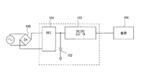
- the diode bridge circuit 100 converts AC power into DC power, and an active power factor correction circuit (PFC).
- the voltage is boosted by 101 and accumulated in the input capacitor 102, and the output of the capacitor 102 is output by the DC-DC converter 103 according to the load (see, for example, Patent Document 1).
- a power supply circuit including an AC-DC conversion circuit that converts AC power of an AC power supply into DC power and a secondary battery that supplies power to the output side of the AC-DC conversion circuit has been proposed (for example, Patent Document 2).
- the secondary battery is connected to the output side of the AC-DC conversion circuit via a charging circuit and a discharging circuit connected in parallel.
- the charging circuit and the discharging circuit control the discharging power and the charging power according to the output current of the AC-DC conversion circuit by the control circuit.
- Patent Document 3 a power supply circuit that rectifies an AC power supply, converts it into a DC voltage, supplies it to a stabilized power supply circuit, and outputs a DC voltage required for a load by the stabilized power supply circuit
- Patent Document 3 a power supply circuit that rectifies an AC power supply, converts it into a DC voltage, supplies it to a stabilized power supply circuit, and outputs a DC voltage required for a load by the stabilized power supply circuit.
- the AC power supply is stepped down and then rectified to charge the charging capacitor, and the charging voltage of the charging capacitor is stabilized when the voltage between the stabilized power supply circuit and the load drops.
- the load is supplied through a circuit.
- the AC power supply voltage drops due to transient peak current flowing into the load, the AC power supply is rectified and the energy stored in the storage unit is supplied to the load.
- An instantaneous voltage drop protection device has been proposed (see, for example, Patent Document 4).
- the narrower the input voltage range of the DC-DC converter 103 the higher the efficiency is possible (by increasing the transformer turns ratio, lowering the breakdown voltage of the secondary side parts and suppressing the current of the primary circuit) Effect).
- the input voltage range of the DC-DC converter is 360 to 400 V and the case where the input voltage range is 250 to 400 V
- the input voltage range is 250 to 400 V.
- the efficiency is improved by about 2% compared to the case of ⁇ 400V.
- the DC-DC converter 103 needs to operate in a wide input voltage range. is there.
- the load power changes periodically, the power that cannot be supplied by the power factor correction circuit 101 is supplied by the input capacitor 102 to absorb the fluctuation of the load power.
- the power fluctuation is not transmitted to the input side.
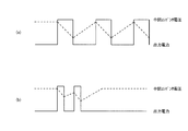
- the voltage of the input capacitor 102 repeatedly decreases and increases periodically as shown by the broken line, and the voltage of the input capacitor 102 is supplied to the load after being stabilized by the DC-DC converter in the subsequent stage.
- the DC-DC converter 103 has to have a wide input range.
- the load power fluctuation is not periodic, for example, after a short-time power fluctuation occurs twice. In many cases, there is no load fluctuation for a while. In the case of such a load fluctuation, the voltage of the input capacitor 102 repeatedly decreases and increases according to the load fluctuation when the load fluctuation occurs as shown by a broken line, but when the load fluctuation does not occur, The output voltage of the power factor correction circuit 101 is held. For this reason, the power conversion efficiency of the DC-DC converter 103 is unnecessarily deteriorated during a period in which no load fluctuation occurs. In addition, the power stored in the input capacitor 102 is charged only by the output voltage of the power factor correction circuit 101.
- the secondary battery is connected only to the output side of the AC-DC conversion circuit, and the secondary battery is charged by converting the AC power of the AC power source into DC power. I can't do it.
- a specific configuration of discharge control of the secondary battery is not disclosed.
- the prior art described in Patent Document 3 merely discloses rectifying an AC power supply to charge a charging capacitor, and does not disclose a specific configuration for discharging control of the charging capacitor.
- the prior art described in Patent Document 4 rectifies an AC power source and stores it in the power storage unit. However, only a DC-DC constant voltage circuit is disclosed as a discharge control unit. A specific configuration is not disclosed.
- the present invention has been made paying attention to the problems of the above-described conventional example, and an object thereof is to provide a power leveling apparatus capable of improving the power conversion efficiency by narrowing the input voltage range. .
- one aspect of a power leveling apparatus includes: a power converter that converts AC power from an AC power source into DC power and supplies the power to a load; and an output side of the power converter. And a power storage unit that supplies DC power.
- the power storage unit is connected between the power storage element and an output side of the power storage element and the power conversion unit, and controls the discharge power according to the output current of the power conversion unit, and charges the power storage element And a charging control unit.
- the charge control unit converts AC power into DC power and charges the power storage element with constant power.
- the discharge control unit monitors the output current of the voltage dividing circuit and the power conversion unit, and sets the divided voltage of the current monitoring unit that draws current from the voltage dividing circuit when the output current is larger than the set current, and the divided voltage of the voltage dividing circuit A discharge current control unit that generates a discharge command signal in comparison with the voltage.
- the input voltage range of the power conversion unit is narrowed by covering the insufficient power that cannot be covered by the power conversion unit due to load power fluctuation by controlling the discharge power of the power storage unit by the discharge control unit.
- the input power can be leveled.
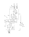
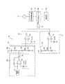
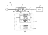
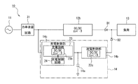
- FIG. 1 is a block diagram showing a first embodiment of a power leveling apparatus according to the present invention. It is a circuit diagram which shows the discharge control part of FIG. It is a circuit diagram which shows the charge control part of FIG. It is a block diagram which shows 2nd Embodiment of the power leveling apparatus which concerns on this invention. It is a block diagram which shows 3rd Embodiment of the power leveling apparatus which concerns on this invention. It is a block diagram which shows a prior art example. It is a time chart which shows the relationship between the load voltage fluctuation
- the power leveling device 10 includes an AC power source 11 that outputs, for example, 230 V AC power, and an AC / DC converter 12 as a power converter that receives AC power from the AC power source 11. And a load 13 to which output power from the AC / DC converter 12 is supplied, and a power storage unit 14 connected in parallel with the AC-DC converter 12.
- the AC / DC converter 12 includes a power factor correction circuit (PFC) 12a and a DC-DC converter 12b.
- the power factor correction circuit 12a has a rectifying function for converting AC power into a DC voltage and an output limiting current so that the input current does not exceed a preset set current.
- the DC-DC converter 12b converts the DC power output from the power factor correction circuit 12a into a DC voltage required by the load 13, for example, 12V DC power, and outputs the DC power to the load 13 via the diode D1.
- the power storage unit 14 includes a power storage element 14 a, a discharge control unit 14 b that discharges the stored power stored in the power storage element 14 a to the output side of the AC / DC converter 12, and AC power input from the AC power supply 11.
- the storage element 14a is a chargeable / dischargeable element, and an electric double layer capacitor, a lithium ion capacitor, an electrolytic capacitor, various batteries (lead, alkali, lithium ion, etc.), and the like can be applied.
- the discharge controller 14b includes an input terminal tin2 to which its own output voltage VA2 is input, and three voltage dividing resistors R11 and R12 connected in series between the input terminal tin2 and the ground. And a voltage dividing circuit 20 having R13, a current monitoring unit 21, and a discharge current control unit 22.
- the current monitoring unit 21 is a permissible upper limit current value output by the AC / DC converter 12 in which the current detection value IA1 input from the current detection unit CD that detects the output current of the AC / DC converter 12 as a voltage value is preset.
- An operational amplifier 21a that sucks current when IA1u or higher is provided.
- a current detection value IA1 having a voltage value is input to an inverting input terminal, and a reference voltage Vref1 corresponding to the allowable upper limit current value IA1u is input to a non-inverting input terminal.
- the output terminal of the operational amplifier 21a is connected to the cathode of the diode 21b, and the anode of the diode 21b is connected to the connection point of the resistors R11 and R12 of the voltage dividing circuit 20. Therefore, the operational amplifier 21a maintains a high level until the current detection value IA1 becomes equal to or higher than the set current value IA1u, and becomes a low level when the current detection value IA1 becomes equal to or higher than the set current value IA1u. Draw current from.
- the discharge current control unit 22 includes an operational amplifier 22a, a PWM signal generation circuit 22b, and a DC / DC converter 22c.
- the connection point of the resistors R12 and R13 of the voltage dividing circuit 20 is connected to the inverting input terminal, and the reference voltage Vref2 corresponding to 12V is input to the non-inverting input terminal.
- the divided voltage Vd input from the operational amplifier 22a from the voltage dividing circuit 20 is equal to or higher than the reference voltage Vref2, a discharge control signal Vc that is at a low level is output, and when the divided voltage Vd becomes lower than the reference voltage Vref2.
- the discharge control signal Vc having a voltage level corresponding to the difference is output.
- the PWM signal generation circuit 22b includes a comparator that compares the discharge control signal Vc output from the operational amplifier 22a with the carrier signal Sca that is a triangular wave signal or a sawtooth wave signal input from the carrier signal generation unit CS.
- the comparator outputs a PWM signal that is turned on while the discharge control signal Vc is above the carrier signal Sca, and that is turned off while the discharge control signal Vc is below the carrier signal.
- DC / DC converter 22c is connected between power storage element 14a and diode D2, and has a permissible range for charging voltage Vb of power storage element 14a with respect to voltage VA1 output from AC / DC converter 12 based on the PWM signal.
- the voltage is increased to a relatively high voltage VA2, and the storage element 14a can be discharged.
- the discharge current control unit 22 is controlled to be in an operation state or a stop state by an operation control signal Smc output from the current monitoring comparator 22d.
- the current detection value IA1 output from the current detection unit CD that detects the output current of the AC / DC converter 12 as a voltage value is supplied to the non-inverting input terminal, and the inverting input terminal is slightly more than the reference voltage Vref1.
- a reference voltage Vref6 set to a low voltage is supplied. Therefore, the comparator 22d outputs the low-level operation control signal Smc to the discharge current control unit 22 in a state where the current detection value IA1 is lower than the reference voltage Vref6, and the discharge current control unit 22 enters an operation stop state.
- the charging control unit 14 c includes a charging circuit 23 and a charging control circuit 24.
- the charging circuit 23 includes a power factor correction circuit 23a and a DC / DC converter 23b.
- the charging circuit 23 converts the AC power from the AC power source 11 into DC power to Charge.
- the constant current control is performed until the charging voltage Vb reaches the set voltage, and the constant voltage control is performed when the set voltage is reached. To do.
- the storage element 14a is a battery
- constant current / constant voltage control is performed in the same manner as the capacitor.
- the DC / DC converter 23b is omitted. Constant power / constant voltage charging is performed only by the rate improvement circuit 23a.
- the charging control circuit 24 monitors the charging voltage Vb of the storage element 14a, and when the charging voltage Vb drops below a preset normal set value Vbu (for example, 70% of the full charging voltage), the AC-DC converter 12 When the output current IA1 is less than the allowable charging current IA1s2 lower than the allowable upper limit current IA1s1, that is, when the power consumption of the load 13 is small, the power charging command Scc is output to the charging circuit 23.
- the charge control circuit 24 determines that the AC-DC converter 12 when the charge voltage Vb of the power storage element 14a falls below the required charge setting value Vbc (for example, 20% of the full charge voltage) lower than the normal setting value Vbu.
- the power charging command Scc is output to the charging circuit 23 regardless of the output current IA1.
- the charging control circuit 24 includes a storage voltage detection unit 25, a first control unit 26, a second control unit 27, and an OR circuit 28.
- the storage voltage detection unit 25 includes a power supply terminal tin2 to which the charging voltage Vb of the storage element 14a is input, and a voltage dividing circuit having voltage dividing resistors R21, R22, and R23 connected in series between the power supply terminal tin2 and the ground. 25a.
- a current monitoring unit 25b is connected to a connection point between the resistors R21 and R22 of the voltage dividing circuit 25a. Further, the stored voltage detection value Vbd is output from the connection point between the resistors R22 and R32 of the voltage dividing circuit 25.
- the current monitoring unit 25b includes an operational amplifier 29 and a diode 30 similarly to the current monitoring unit 21 of the discharge control unit 14b.
- the operational amplifier 29 the current detection value IA1 of the current sensor CD is supplied to the non-inverting input terminal, and the charging allowable current IA1s2 lower than the allowable upper limit current IA1s1 of the reference voltage Vref3 (the output current IA1 of the AC-DC converter 12) is supplied to the inverting input terminal. Is supplied).
- the diode 30 has an anode connected to the output terminal of the operational amplifier 29 and a cathode connected to a connection point between the resistors R21 and R22 of the voltage dividing circuit 25a.
- the first control unit 26 includes a comparator 26a.
- the stored voltage detection value Vbd is input to the inverting input terminal, and the reference voltage Vref4 is supplied to the non-inverting input terminal.
- Reference voltage Vref4 is set to a voltage value corresponding to, for example, 70% of full charge voltage Vbmax of power storage element 14a. Therefore, a voltage drop detection signal Svr that changes from a low level to a high level when the stored voltage detection value Vbd falls below the reference voltage Vref4 is output from the comparator 26a to the OR circuit 28.
- the second control unit 27 includes a voltage dividing circuit 27a that divides the storage voltage Vb of the storage element 14a and a comparator 27b.
- the voltage dividing circuit 27a includes an input terminal tin3 to which the stored voltage Vb of the power storage element 14a is input, and voltage dividing resistors R24 and R25 connected between the input terminal tin3 and the ground.
- the stored voltage detection value Vbd2 is output from the connection point of the voltage dividing resistors R24 and R25.
- the comparator 27b the stored voltage detection value Vbd of the voltage dividing circuit 27a is input to the inverting input terminal, and the reference voltage Vref5 is input to the non-inverting input terminal.
- the reference voltage Vref5 is set to a voltage value corresponding to, for example, 20% of the full charge voltage Vbmax of the storage element 14a.
- the charging voltage Vb of the storage element 14a is charged to a state close to the full charge pressure Vbmax.
- the charge control unit 14c of the power storage unit 14 is such that the divided voltage Vbd of the voltage dividing circuit 25a is equal to or higher than the reference voltage Vref4 of the comparator 26a of the first control unit 26, and the voltage drop detection signal output from the comparator 26a. Svr becomes low level. Further, the charge required detection signal Svc output from the comparator 27b of the second control unit 27 is also at a low level. For this reason, the power charging command Scc is not output from the OR circuit 28, and the charging circuit 23 stops operating.
- the current IA1 output from the AC / DC converter 12 is the discharge controller 14b. Is lower than the reference voltage Vref6 of the current monitoring comparator 22d. For this reason, the operation control signal Smc output from the comparator 22d is at a low level, the discharge current control unit 22 is in an operation stopped state, and the DC / DC converter 22c is stopped in operation. As a result, while the power consumption of the load 13 is small, only the AC / DC converter 12 is in an operating state when the charging process of the power storage element 14a is not performed.
- the current IA1 output from the AC / DC converter 12 increases and is higher than the reference voltage Vref6 of the current monitoring comparator 22d of the discharge control unit 14b.
- the operation control signal Smc output from the current monitoring comparator 22d becomes high level, and the discharge current control unit 22
- the operating state is entered, and the DC / DC converter 22c enters the operating state.
- the current IA1 output from the AC / DC converter 12 is lower than the reference voltage Vref1 of the operational amplifier 21a of the current monitoring unit 21 of the discharge control unit 14b. For this reason, the output of the operational amplifier 21a is maintained at a high level, and the current of the voltage dividing circuit 20 is not drawn through the diode 21b.
- the divided voltage Vd divided by the resistors R11 and R12 and R13 of the voltage dividing circuit 20 is supplied to the inverting input terminal of the operational amplifier 22a of the discharge current control unit 22.
- the discharge control signal Vc having a low voltage level corresponding to the difference from the reference voltage Vref2 is output from the operational amplifier 22a.
- a PWM signal corresponding to the voltage level of the discharge control signal Vc is output from the PWM signal generation circuit 22b to the DC / DC converter 22c, and the output voltage of the DC / DC converter 22c increases.
- the increase in the output voltage of the DC / DC converter 22c increases, for example, to 11V so that the diode D2 is not turned on when the voltage of the load 13 is 12V, and the power storage element 14a shares the power consumption of the load 13. Prepare for.
- the discharge control unit 14b In the current monitoring unit 21, the output of the operational amplifier 21a becomes a low level, that is, the ground potential, and the current of the voltage dividing circuit 20 is drawn through the diode 21b. For this reason, the divided voltage Vd output between the resistors R22 and R23 of the voltage dividing circuit 20 becomes sufficiently smaller than the reference voltage Vref2 of the operational amplifier 22a, and the voltage level of the discharge control signal Vc output from the operational amplifier 22a increases rapidly. To do. Therefore, a PWM signal having a wide ON state is obtained from the PWM signal generation circuit 22b, and this PWM signal is supplied to the DC / DC converter 22c.
- the DC / DC converter 22c boosts the storage voltage Vb of the storage element 14a to the reference voltage VA2 in accordance with the width of the PWM signal in the on state. For this reason, the output current IA2 corresponding to the shortage of the power consumption of the load 13 is output from the power storage element 14a to the load 13 side through the DC / DC converter 22c of the discharge control unit 14b and further via the diode D2. It is added to the output current IA1 of the DC converter 12 and supplied to the load 13. For this reason, the amount of current that cannot be covered by the AC / DC converter 12 can be covered by the amount of current from the storage element 14a. At this time, since the output voltage to the load 13 maintains the reference voltage VA1, the power consumption required by the load 13 can be supplied.
- the charging voltage Vb of the power storage element 14a decreases, and falls below the reference voltage Vref4 of the first control unit 26 of the charging control unit 14c.
- the output current IA1 of the AC / DC converter 12 monitored by the current monitoring unit 25b exceeds the charge allowable current IA1s2
- the output of the operational amplifier 29 is at a high level. Therefore, current is supplied to the connection point between the resistors R21 and R22 of the voltage dividing circuit 25a via the diode 30, so that the divided voltage Vd at the connection point between the resistors R22 and R23 is higher than the reference voltage Vref4 of the operational amplifier 26a.
- the stored voltage drop detection signal Svr is at a low level.
- the charge-required detection signal Svc output from the comparator 27b of the second control unit 27 is also maintained at a low level, so that the power charging command Scc output from the OR circuit 18 is maintained at a low level.
- the charging process of the storage element 14a is not executed. In this state, when the power consumption of the load 13 decreases and the voltage value of the output current IA1 output from the AC / DC converter 12 decreases below the reference voltage Vref3, the output of the operational amplifier 29 becomes low level, and the voltage dividing circuit The supply of current to the connection point of the resistors R21 and R22 of 25a is stopped.
- the current drop detection signal Svr output from the comparator 26 a of the first control unit 26 becomes high level, and a high level power charge command Scc is output from the OR circuit 28 to the DC / DC converter 23 b of the charging circuit 23.
- the charging circuit 23 converts the AC power from the AC power supply 11 into a DC current and steps down the voltage to charge the storage element 14a.
- the storage element 14a is an electric double layer capacitor or a lithium ion capacitor
- constant current control is performed when the charging voltage is less than the set voltage
- constant voltage control is performed when the set voltage is reached.
- the constant voltage control may be performed when the power storage element 14a is configured by a battery, and when the power storage element 14a is configured by an electrolytic capacitor, the DC / DC converter 23b is omitted to improve the power factor. Only the circuit 23a may be provided.
- the AC power of the AC power supply 11 is directly supplied to the AC / DC converter 12, and the AC power is full-wave rectified by the power factor improving circuit 12 a of the AC / DC converter 12.
- power factor improvement processing is performed.
- the DC / DC converter 12b steps down the DC voltage required by the load 13 and outputs the voltage to the load 13 via the diode D1.
- the necessary current of the load 13 can be provided only by the AC / DC converter 12, only the AC / DC converter 12 is driven. Then, the current required by the load 13 is monitored by the current monitoring unit 21 of the discharge control unit 14b.
- the discharge control unit 14b of the power storage unit 14 is driven to boost the stored voltage Vb of the power storage element 14a to the set voltage VA2. .
- a discharge current corresponding to a current exceeding the current that can be covered by the AC / DC converter 12 is supplied to the load 13.
- the AC / DC converter 12 it is not necessary to operate the AC / DC converter 12 so as to cover the entire current range required by the load 13, but only by performing power conversion so as to output a voltage and current that can be generated with constant input power. Well, it does not cause fluctuations in input power. As a result, the input voltage range of the AC / DC converter 12 can be narrowed to improve the power conversion efficiency, and at the same time, the current that cannot be covered by the AC / DC converter 12 due to fluctuations in the power consumption of the load 13 is stored. This can be covered by discharging the power stored in the element 14a.
- the conversion efficiency when both the AC / DC converter 12 and the discharge control unit 14b of the power storage unit 14 are operating can be improved by about 1.0% with respect to the conversion efficiency of the conventional example described above.
- the conversion efficiency of the conventional example can be improved by 2.0%. Therefore, according to the first embodiment, the power consumption fluctuation of the load does not affect the input side of the AC / DC converter 12, the input voltage of the AC / DC converter 12 can be leveled, Conversion efficiency can be improved.
- the storage element is charged using DC power output from the AC / DC converter. That is, in 2nd Embodiment, as shown in FIG. 4, the charge control part 14c of the electrical storage part 14 is provided in parallel with the discharge control part 14b. For this reason, in the charging control unit 14c, the power factor correction circuit constituting the charging circuit 23 is omitted and only the DC / DC converter 23b is configured.
- the DC / DC converter 23b is controlled by a power charge command from a charge control circuit 24 having the same configuration as that of the first embodiment. Further, the diode D2 is omitted.
- Other configurations are the same as those in FIGS. 1 to 3 of the first embodiment described above.
- the input power is leveled in the same manner as in the first embodiment except that the power storage element 14a in the power storage unit 14 is charged by the output power of the AC / DC converter 12. be able to. For this reason, also in 2nd Embodiment, the effect similar to 1st Embodiment mentioned above can be acquired. Therefore, in the state where the AC / DC converter 12 and the discharge control unit 14b of the power storage unit 14 are operating, the power conversion efficiency can be improved by 1.0% as compared with the conventional example described above. Furthermore, the power conversion efficiency when the power consumption of the load 13 can be covered only by the AC / DC converter 12 can be improved by 2.0%.
- the power factor correction circuit is shared. That is, in the third embodiment, as shown in FIG. 5, the AC power source 11 is made independent of the power factor improvement circuit provided in the AC / DC converter 12 and the charging control unit 14 c in the first embodiment.
- a power factor correction circuit 31 is connected. The output of the power factor correction circuit 31 is supplied to the DC / DC converter in the DC / DC converter 12b and the charge control unit 14c of the power storage unit 14.
- Other configurations are the same as those in the first embodiment.
- the electric power of the charging control unit 14c has a small capacity, and when a power factor correction circuit is provided independently, the charger efficiency is lowered. For this reason, by setting it as the structure of 3rd Embodiment, the large-capacity power factor improvement circuit of the DC / DC converter 12b can be used as a power factor improvement circuit of the charge control part 14c.
- the power conversion efficiency in the state where the DC / DC converter 12b and the discharge control unit 14b are simultaneously operated can be improved by 1.3% compared to the power conversion efficiency of the conventional example described above. Furthermore, the conversion efficiency during a period in which only the DC / DC converter 12b operates and there is no load fluctuation can be improved by 2.0%.
- the present invention is not limited to this, and the present invention is also applied to a case where the power conversion system is connected in parallel to a plurality of systems. Can be applied.
- SYMBOLS 10 Electric power leveling apparatus, 11 ... AC power supply, 12 ... AC / DC converter, 13 ... Load, 14 ... Power storage part, 14a ... Power storage element, 14b ... Discharge control part, 14c ... Charge control part, 20 ... Partial pressure Circuit 21... Current monitoring unit 21 a. Operational amplifier 22... Discharge current control unit 22 a. Operational amplifier 22 b... PWM signal generation circuit 22 c DC / DC converter 25 25 storage voltage detection unit 25 a. 25b ... Current monitoring unit, 26 ... First control unit, 26a ... Comparator, 27 ... Second control unit, 27a ... Comparator, 28 ... OR circuit, 31 ... Power factor improvement circuit
Landscapes
- Engineering & Computer Science (AREA)
- Power Engineering (AREA)
- Charge And Discharge Circuits For Batteries Or The Like (AREA)
- Dc-Dc Converters (AREA)
- Direct Current Feeding And Distribution (AREA)
- Rectifiers (AREA)
Abstract
入力電圧範囲を狭くして電力変換効率を向上させることができる電力平準化装置を提供する。交流電源(11)からの交流電力を直流電力に変換して負荷に供給する電力変換部(12)と、電力変換部の出力側に直流電力を供給する蓄電部(14)とを備えている。蓄電部は、蓄電素子(14a)と、この蓄電素子および電力変換部の出力側との間に接続され、電力変換部の出力電流に応じて放電電力を制御する放電制御部(14b)と、蓄電素子を充電する充電制御部(14c)とを備えている。充電制御部は、蓄電素子の充電電圧が設定値以下となったときに、交流電力を直流電力に変換して蓄電素子を定電力充電する。放電制御部は、分圧回路と、電力変換部の出力電流を監視し、出力電流が設定電流より大きいときに分圧回路から電流を引き抜く電流監視部と、分圧回路の分圧電圧を設定電圧と比較して放電指令信号を生成する放電電流制御部とを備えている。
Description
本発明は、負荷電力変動を抑制して電力平準化を行う電力平準化装置に関する。
近年、クラウドコンピューティングやビッグデータ解析需要の拡大に伴い、データセンター内において、複数のコンピュータが同期して動作するシステムが増加している。コンピュータは、CPUの動作状態等により瞬間的に消費電力が変動するため、複数台のコンピュータが同調して動作すると瞬間的に大きな消費電力が発生しその電力を供給する入力系統に負担が掛かっている(例えば、トランス、発電機等のうなり、ケーブルやブレーカなどの配電設備への過大なストレス)。
一方、高速化・大容量かにより電算機システム全体の消費電力が肥大化しており、電力供給ユニット(PSU)等の電力変換部の損失低減要求が強くなっている。
一方、高速化・大容量かにより電算機システム全体の消費電力が肥大化しており、電力供給ユニット(PSU)等の電力変換部の損失低減要求が強くなっている。
負荷電力変動を入力側に伝えないように電力平準化を行うために、図6に示すように、ダイオードブリッジ回路100で交流電力を直流電力に変換し、アクティブ型の力率改善回路(PFC)101で昇圧して入力コンデンサ102に蓄積し、このコンデンサ102の出力をDC-DCコンバータ103で負荷に応じた直流電力を出力するようにしている(例えば、特許文献1参照)。
また、交流電源の交流電力を直流電力に変換するAC-DC変換回路と、AC-DC変換回路の出力側に電力を供給する二次電池とを備えた電源回路が提案されている(例えば、特許文献2参照)。この特許文献2に記載された先行技術では、二次電池は並列に接続された充電回路及び放電回路を介してAC-DC変換回路の出力側に接続されている。そして、充電回路及び放電回路が、制御回路によって、AC-DC変換回路の出力電流に応じて放電電力及び充電電力を制御するようにしている。
また、交流電源の交流電力を直流電力に変換するAC-DC変換回路と、AC-DC変換回路の出力側に電力を供給する二次電池とを備えた電源回路が提案されている(例えば、特許文献2参照)。この特許文献2に記載された先行技術では、二次電池は並列に接続された充電回路及び放電回路を介してAC-DC変換回路の出力側に接続されている。そして、充電回路及び放電回路が、制御回路によって、AC-DC変換回路の出力電流に応じて放電電力及び充電電力を制御するようにしている。
さらに、交流電源を整流して直流電圧に変換して安定化電源回路に供給し、この安定化電源回路で負荷に必要な直流電圧を出力する電源回路が提案されている(例えば、特許文献3参照)。この特許文献3に記載された先行技術では、交流電源を降圧してから整流して充電用コンデンサを充電し、安定化電源回路及び負荷間の電圧低下時に充電用コンデンサの充電電圧を、安定化回路を介して負荷に供給するようにしている。
また、正常時は交流電力を整流した直流主電圧を負荷に供給し、負荷に流れ込む過渡ピーク電流による交流電源電圧の低下時に、交流電源を整流して蓄積部に蓄えられたエネルギーを負荷に供給する瞬時電圧低下保護装置が提案されている(例えば、特許文献4参照)。
また、正常時は交流電力を整流した直流主電圧を負荷に供給し、負荷に流れ込む過渡ピーク電流による交流電源電圧の低下時に、交流電源を整流して蓄積部に蓄えられたエネルギーを負荷に供給する瞬時電圧低下保護装置が提案されている(例えば、特許文献4参照)。
ところで、一般的に、DC-DCコンバータ103の入力電圧範囲が狭いほど高効率化が可能である(トランス巻数比を上げることで、2次側部品の低耐圧化、1次回路の電流抑制による効果等)。例えば、DC-DCコンバータの入力電圧範囲が360~400Vである場合と、入力電圧範囲が250~400Vである場合とを比較すると、入力電圧範囲が360~400Vの方が、入力電圧範囲が250~400Vである場合に比較して2%程度効率が良くなる。
しかし、上述した複数のコンピュータが同期して動作するシステムのように負荷変動が大きい場合には、DC-DCコンバータ103は広い入力電圧範囲で動作する必要があるため変換効率が低下するという課題がある。
しかし、上述した複数のコンピュータが同期して動作するシステムのように負荷変動が大きい場合には、DC-DCコンバータ103は広い入力電圧範囲で動作する必要があるため変換効率が低下するという課題がある。
すなわち、図7(a)で実線図示のように、負荷電力が周期的に変化する場合には、力率改善回路101で賄えない電力を入力コンデンサ102で賄って負荷電力の変動を吸収し、入力側に電力変動を伝達させないようにする。このため、入力コンデンサ102の電圧は、破線図示のように周期的に減少および増加を繰り返し、この入力コンデンサ102の電圧を後段のDC-DCコンバータにより、電圧を一定化させて負荷に供給する。この場合には、DC-DCコンバータ103を広い入力範囲とせざるを得ない。
しかしながら、上述した複数のコンピュータが同期して動作するシステムでは、図7(b)で実線図示のように、負荷電力の変動が周期的ではなく、例えば短時間の電力変動が2回生じた後に、しばらく負荷変動がない状態が継続する場合が多い。このような負荷変動の場合、入力コンデンサ102の電圧は、破線図示のように負荷変動が生じたときに、負荷変動に応じた減少および増加を繰り返すが、負荷変動を生じていない場合には、力率改善回路101の出力電圧を保持することになる。このため、負荷変動を生じていない期間でDC-DCコンバータ103の電力変換効率が無駄に悪くなってしまう。しかも、入力コンデンサ102に蓄積する電力は、力率改善回路101の出力電圧のみで充電される。
しかしながら、上述した複数のコンピュータが同期して動作するシステムでは、図7(b)で実線図示のように、負荷電力の変動が周期的ではなく、例えば短時間の電力変動が2回生じた後に、しばらく負荷変動がない状態が継続する場合が多い。このような負荷変動の場合、入力コンデンサ102の電圧は、破線図示のように負荷変動が生じたときに、負荷変動に応じた減少および増加を繰り返すが、負荷変動を生じていない場合には、力率改善回路101の出力電圧を保持することになる。このため、負荷変動を生じていない期間でDC-DCコンバータ103の電力変換効率が無駄に悪くなってしまう。しかも、入力コンデンサ102に蓄積する電力は、力率改善回路101の出力電圧のみで充電される。
また、特許文献2に記載された先行技術には、二次電池がAC-DC変換回路の出力側のみに接続されており、二次電池を交流電源の交流電力を直流電力に変換して充電することはできない。その上、二次電池の放電制御の具体的構成は開示されていない。
さらに、特許文献3に記載された先行技術には、交流電源を整流して充電用コンデンサを充電することが開示されているだけで、充電用コンデンサの放電制御の具体的構成は開示されていない。
また、特許文献4に記載された先行技術には、交流電源を整流して蓄電部に蓄積するが、放電制御部としてDC-DC定電圧回路が開示されているだけで蓄電部の放電制御の具体的構成は開示されていない。
さらに、特許文献3に記載された先行技術には、交流電源を整流して充電用コンデンサを充電することが開示されているだけで、充電用コンデンサの放電制御の具体的構成は開示されていない。
また、特許文献4に記載された先行技術には、交流電源を整流して蓄電部に蓄積するが、放電制御部としてDC-DC定電圧回路が開示されているだけで蓄電部の放電制御の具体的構成は開示されていない。
そこで、本発明は、上述した従来例の課題に着目してなされたものであり、入力電圧範囲を狭くして電力変換効率を向上させることができる電力平準化装置を提供することを目的としている。
上記目的を達成するために、本発明に係る電力平準化装置の一態様は、交流電源からの交流電力を直流電力に変換して負荷に供給する電力変換部と、電力変換部の出力側に直流電力を供給する蓄電部とを備えている。蓄電部は、蓄電素子と、該蓄電素子および電力変換部の出力側との間に接続され、電力変換部の出力電流に応じて放電電力を制御する放電制御部と、前記蓄電素子を充電する充電制御部とを備えている。充電制御部は、蓄電素子の充電電圧が設定値以下となったときに、交流電力を直流電力に変換して当該蓄電素子を定電力充電する。放電制御部は、分圧回路と、電力変換部の出力電流を監視し、出力電流が設定電流より大きいときに分圧回路から電流を引き抜く電流監視部と、分圧回路の分圧電圧を設定電圧と比較して放電指令信号を生成する放電電流制御部とを備えている。
本発明の一態様によれば、負荷電力変動による電力変換部で賄えない不足電力分を放電制御部で蓄電部の放電電力を制御して賄うことにより、電力変換部の入力電圧範囲を狭くして入力電力を平準化することができる。
次に、図面を参照して、本発明の一実施の形態を説明する。以下の図面の記載において、同一又は類似の部分には同一又は類似の符号を付している。ただし、図面は模式的なものである。
また、以下に示す実施の形態は、本発明の技術的思想を具体化するための装置や方法を例示するものであって、本発明の技術的思想は、構成部品の構造、配置等を下記のものに特定するものでない。本発明の技術的思想は、特許請求の範囲に記載された請求項が規定する技術的範囲内において、種々の変更を加えることができる。
また、以下に示す実施の形態は、本発明の技術的思想を具体化するための装置や方法を例示するものであって、本発明の技術的思想は、構成部品の構造、配置等を下記のものに特定するものでない。本発明の技術的思想は、特許請求の範囲に記載された請求項が規定する技術的範囲内において、種々の変更を加えることができる。
まず、本発明の一の態様を表す電力平準化装置の第1の実施形態について図1および図2を伴って説明する。
電力平準化装置10は、図1に示すように、例えば230Vの交流電力を出力する交流電源11と、この交流電源11からの交流電力が入力される電力変換部としてのAC/DC変換器12と、このAC/DC変換器12からの出力電力が供給される負荷13と、AC-DC変換器12と並列に接続された蓄電部14とを備えている。
ここで、AC/DC変換器12は、力率改善回路(PFC)12aとDC-DCコンバータ12bとで構成されている。力率改善回路12aは、交流電力を直流電圧に変換する整流機能と、入力電流が予め設定した設定電流を超えないように、出力制限電流が設定されている。
電力平準化装置10は、図1に示すように、例えば230Vの交流電力を出力する交流電源11と、この交流電源11からの交流電力が入力される電力変換部としてのAC/DC変換器12と、このAC/DC変換器12からの出力電力が供給される負荷13と、AC-DC変換器12と並列に接続された蓄電部14とを備えている。
ここで、AC/DC変換器12は、力率改善回路(PFC)12aとDC-DCコンバータ12bとで構成されている。力率改善回路12aは、交流電力を直流電圧に変換する整流機能と、入力電流が予め設定した設定電流を超えないように、出力制限電流が設定されている。
DC-DCコンバータ12bは、力率改善回路12aから出力される直流電力を負荷13が必要とする直流電圧例えば12Vの直流電力に変換して負荷13にダイオードD1を介して出力する。
蓄電部14は、蓄電素子14aと、蓄電素子14aに蓄電された蓄電電力をAC/DC変換器12の出力側に放電する放電制御部14bと、交流電源11から交流電力が入力されて蓄電素子14aを充電する充電制御部14cと、を備えている。
蓄電素子14aは、充放電可能な素子であって、電気2重層キャパシタ、リチウムイオンキャパシタ、電解コンデンサ、各種バッテリ(鉛、アルカリ、リチウムイオン他)等を適用することができる。
蓄電部14は、蓄電素子14aと、蓄電素子14aに蓄電された蓄電電力をAC/DC変換器12の出力側に放電する放電制御部14bと、交流電源11から交流電力が入力されて蓄電素子14aを充電する充電制御部14cと、を備えている。
蓄電素子14aは、充放電可能な素子であって、電気2重層キャパシタ、リチウムイオンキャパシタ、電解コンデンサ、各種バッテリ(鉛、アルカリ、リチウムイオン他)等を適用することができる。
放電制御部14bは、図2に示すように、自身の出力電圧VA2が入力される入力端子tin2と、この入力端子tin2とグランドとの間に直列に接続された3つの分圧抵抗R11、R12およびR13を有する分圧回路20と、電流監視部21と、放電電流制御部22とを備えている。
電流監視部21は、AC/DC変換器12の出力電流を電圧値として検出する電流検出部CDから入力される電流検出値IA1が予め設定したAC/DC変換器12が出力する許容上限電流値IA1u以上であるとき電流を吸引するオペアンプ21aを備えている。このオペアンプ21aは、反転入力端子に電圧値でなる電流検出値IA1が入力され、非反転入力端子に許容上限電流値IA1uに相当する参照電圧Vref1が入力されている。そして、このオペアンプ21aの出力端子がダイオード21bのカソードに接続され、ダイオード21bのアノードが分圧回路20の抵抗R11およびR12の接続点に接続されている。したがって、オペアンプ21aは、電流検出値IA1が設定電流値IA1u以上となるまではハイレベルを維持し、電流検出値IA1が設定電流値IA1u以上となったときにローレベルとなって分圧回路20から電流を引き込む。
電流監視部21は、AC/DC変換器12の出力電流を電圧値として検出する電流検出部CDから入力される電流検出値IA1が予め設定したAC/DC変換器12が出力する許容上限電流値IA1u以上であるとき電流を吸引するオペアンプ21aを備えている。このオペアンプ21aは、反転入力端子に電圧値でなる電流検出値IA1が入力され、非反転入力端子に許容上限電流値IA1uに相当する参照電圧Vref1が入力されている。そして、このオペアンプ21aの出力端子がダイオード21bのカソードに接続され、ダイオード21bのアノードが分圧回路20の抵抗R11およびR12の接続点に接続されている。したがって、オペアンプ21aは、電流検出値IA1が設定電流値IA1u以上となるまではハイレベルを維持し、電流検出値IA1が設定電流値IA1u以上となったときにローレベルとなって分圧回路20から電流を引き込む。
放電電流制御部22は、オペアンプ22aと、PWM信号生成回路22bと、DC/DCコンバータ22cとで構成されている。
オペアンプ22aは、反転入力端子に分圧回路20の抵抗R12およびR13の接続点が接続され、非反転入力端子に12Vに相当する参照電圧Vref2が入力されている。そして、このオペアンプ22aから分圧回路20から入力される分圧電圧Vdが参照電圧Vref2以上であるときにローレベルとなる放電制御信号Vcを出力し、分圧電圧Vdが参照電圧Vref2未満となると、その差分に応じた電圧レベルの放電制御信号Vcを出力する。
オペアンプ22aは、反転入力端子に分圧回路20の抵抗R12およびR13の接続点が接続され、非反転入力端子に12Vに相当する参照電圧Vref2が入力されている。そして、このオペアンプ22aから分圧回路20から入力される分圧電圧Vdが参照電圧Vref2以上であるときにローレベルとなる放電制御信号Vcを出力し、分圧電圧Vdが参照電圧Vref2未満となると、その差分に応じた電圧レベルの放電制御信号Vcを出力する。
PWM信号生成回路22bは、オペアンプ22aから出力される放電制御信号Vcとキャリア信号生成部CSから入力される三角波信号または鋸歯状波信号でなるキャリア信号Scaと比較するコンパレータで構成されている。このコンパレータから放電制御信号Vcがキャリア信号Scaを上回っている間にオン状態となり、放電制御信号Vcがキャリア信号を下回っている間にオフ状態となるPWM信号が出力される。
DC/DCコンバータ22cは、蓄電素子14aとダイオードD2との間に接続され、蓄電素子14aの充電電圧VbをPWM信号に基づいてAC/DC変換器12から出力される電圧VA1に対して許容範囲程度高い電圧VA2に昇圧し、蓄電素子14aの放電を可能とする。
DC/DCコンバータ22cは、蓄電素子14aとダイオードD2との間に接続され、蓄電素子14aの充電電圧VbをPWM信号に基づいてAC/DC変換器12から出力される電圧VA1に対して許容範囲程度高い電圧VA2に昇圧し、蓄電素子14aの放電を可能とする。
ここで、放電電流制御部22は、電流監視用のコンパレータ22dから出力される動作制御信号Smcによって動作状態と停止状態とに制御される。コンバレータ22dは、非反転入力端子に、AC/DC変換器12の出力電流を電圧値として検出する電流検出部CDから出力される電流検出値IA1が供給され、反転入力端子に参照電圧Vref1より僅かに低い電圧に設定された参照電圧Vref6が供給されている。
したがって、コンパレータ22dは、電流検出値IA1が参照電圧Vref6を下回っている状態では、ローレベルの動作制御信号Smcを放電電流制御部22に出力し、放電電流制御部22は動作停止状態となる。これに対して、電流検出値IA1が参照電圧Vref6を上回っている状態では、コンパレータ22dからハイレベルの動作制御信号Smcが放電電流制御部22に出力され、放電電流制御部22は動作状態となる。
したがって、コンパレータ22dは、電流検出値IA1が参照電圧Vref6を下回っている状態では、ローレベルの動作制御信号Smcを放電電流制御部22に出力し、放電電流制御部22は動作停止状態となる。これに対して、電流検出値IA1が参照電圧Vref6を上回っている状態では、コンパレータ22dからハイレベルの動作制御信号Smcが放電電流制御部22に出力され、放電電流制御部22は動作状態となる。
充電制御部14cは、図1に示すように、充電回路23と、充電制御回路24とを有する。充電回路23は、力率改善回路23aとDC/DCコンバータ23bとで構成され、電力充電指令Sccが入力されたときに、交流電源11からの交流電力を直流電力に変換して蓄電素子14aを充電する。
このときの充電モードとしては、蓄電素子14aが電気2重層キャパシタやリチウムイオンキャパシタである場合には、充電電圧Vbが設定電圧に達するまでは定電流制御を行い、設定電圧に達すると定電圧制御を行なう。また、蓄電素子14aが各種バッテリであるときにもキャパシタと同様に定電流・定電圧制御を行い、さらに、蓄電素子14aが電解コンデンサである場合には、DC/DCコンバータ23bを省略して力率改善回路23aのみで定電力・定電圧充電を行う。
このときの充電モードとしては、蓄電素子14aが電気2重層キャパシタやリチウムイオンキャパシタである場合には、充電電圧Vbが設定電圧に達するまでは定電流制御を行い、設定電圧に達すると定電圧制御を行なう。また、蓄電素子14aが各種バッテリであるときにもキャパシタと同様に定電流・定電圧制御を行い、さらに、蓄電素子14aが電解コンデンサである場合には、DC/DCコンバータ23bを省略して力率改善回路23aのみで定電力・定電圧充電を行う。
充電制御回路24は、蓄電素子14aの充電電圧Vbを監視し、充電電圧Vbが予め設定した通常設定値Vbu(満充電電圧の例えば70%)以下に低下したときに、AC-DC変換器12の出力電流IA1が許容上限電流IA1s1より低い充電許容電流IA1s2未満であるとき、すなわち負荷13の消費電力が小さいときに電力充電指令Sccを充電回路23に出力する。
また、充電制御回路24は、蓄電素子14aの充電電圧Vbが通常設定値Vbuより低い要充電設定値Vbc(例えば満充電電圧の例えば20%)以下に低下したときに、AC-DC変換器12の出力電流IA1にかかわらず電力充電指令Sccを充電回路23に出力する。
また、充電制御回路24は、蓄電素子14aの充電電圧Vbが通常設定値Vbuより低い要充電設定値Vbc(例えば満充電電圧の例えば20%)以下に低下したときに、AC-DC変換器12の出力電流IA1にかかわらず電力充電指令Sccを充電回路23に出力する。
ここで、充電制御回路24は、図3に示すように、蓄電電圧検出部25と、第1制御部26と、第2制御部27と、オア回路28とを備えている。
蓄電電圧検出部25は、蓄電素子14aの充電電圧Vbが入力される電源端子tin2と、この電源端子tin2とグランドとの間に直列接続された分圧抵抗R21、R22およびR23を有する分圧回路25aを備えている。
この分圧回路25aの抵抗R21およびR22の接続点には電流監視部25bが接続されている。また、分圧回路25の抵抗R22およびR32の接続点から蓄電電圧検出値Vbdが出力される。
蓄電電圧検出部25は、蓄電素子14aの充電電圧Vbが入力される電源端子tin2と、この電源端子tin2とグランドとの間に直列接続された分圧抵抗R21、R22およびR23を有する分圧回路25aを備えている。
この分圧回路25aの抵抗R21およびR22の接続点には電流監視部25bが接続されている。また、分圧回路25の抵抗R22およびR32の接続点から蓄電電圧検出値Vbdが出力される。
ここで、電流監視部25bは、放電制御部14bの電流監視部21と同様にオペアンプ29及びダイオード30を有する。オペアンプ29は、非反転入力端子に電流センサCDの電流検出値IA1が供給され、反転入力端子に参照電圧Vref3(AC-DC変換器12の出力電流IA1の許容上限電流IA1s1より低い充電許容電流IA1s2に相当する電圧)が供給されている。また、ダイオード30はアノードがオペアンプ29の出力端子に接続され、カソードが分圧回路25aの抵抗R21及びR22の接続点に接続されている。
第1制御部26は、コンパレータ26aを備えている。このコンパレータ26aは、反転入力端子に蓄電電圧検出値Vbdが入力され、非反転入力端子に参照電圧Vref4が供給されている。参照電圧Vref4は、蓄電素子14aの満充電電圧Vbmaxの例えば70%に相当する電圧値に設定されている。したがって、コンパレータ26aから蓄電電圧検出値Vbdが参照電圧Vref4を下回ったときにローレベルからハイレベルとなる電圧低下検出信号Svrがオア回路28に出力される。
第2制御部27は、蓄電素子14aの蓄電電圧Vbを分圧する分圧回路27aと、コンパレータ27bを備えている。
第2制御部27は、蓄電素子14aの蓄電電圧Vbを分圧する分圧回路27aと、コンパレータ27bを備えている。
分圧回路27aは、蓄電素子14aの蓄電電圧Vbが入力される入力端子tin3と、この入力端子tin3とグランドとの間に接続された分圧抵抗R24およびR25とで構成されている。そして、分圧抵抗R24およびR25の接続点から蓄電電圧検出値Vbd2が出力される。
コンパレータ27bは、反転入力端子に分圧回路27aの蓄電電圧検出値Vbdが入力され、非反転入力端子に参照電圧Vref5が入力されている。この参照電圧Vref5は、蓄電素子14aの満充電電圧Vbmaxの例えば20%に相当する電圧値に設定されている。したがって、コンパレータ27bから蓄電電圧検出値Vbd2が参照電圧Vref5を下回ったときにローレベルからハイレベルに転換する要充電検出信号Svcがオア回路28に出力される。
オア回路28は、第1制御部26の電圧低下検出信号Svrおよび第2制御部27の要充電検出信号Svcの何れかがハイレベルとなったときに、ハイレベルとなる充電指令信号Scを充電回路CHに出力する。
コンパレータ27bは、反転入力端子に分圧回路27aの蓄電電圧検出値Vbdが入力され、非反転入力端子に参照電圧Vref5が入力されている。この参照電圧Vref5は、蓄電素子14aの満充電電圧Vbmaxの例えば20%に相当する電圧値に設定されている。したがって、コンパレータ27bから蓄電電圧検出値Vbd2が参照電圧Vref5を下回ったときにローレベルからハイレベルに転換する要充電検出信号Svcがオア回路28に出力される。
オア回路28は、第1制御部26の電圧低下検出信号Svrおよび第2制御部27の要充電検出信号Svcの何れかがハイレベルとなったときに、ハイレベルとなる充電指令信号Scを充電回路CHに出力する。
次に、上記第1の実施形態の動作を説明する。
今、蓄電素子14aの充電電圧Vbが満充電圧Vbmaxに近い状態に充電されているものとする。
この状態では、蓄電部14の充電制御部14cは、分圧回路25aの分圧電圧Vbdが第1制御部26のコンパレータ26aの参照電圧Vref4以上であり、コンパレータ26aから出力される電圧低下検出信号Svrがローレベルとなる。また、第2制御部27のコンパレータ27bから出力される要充電検出信号Svcもローレベルとなっている。このため、オア回路28から電力充電指令Sccは出力されず、充電回路23は作動を停止している。
今、蓄電素子14aの充電電圧Vbが満充電圧Vbmaxに近い状態に充電されているものとする。
この状態では、蓄電部14の充電制御部14cは、分圧回路25aの分圧電圧Vbdが第1制御部26のコンパレータ26aの参照電圧Vref4以上であり、コンパレータ26aから出力される電圧低下検出信号Svrがローレベルとなる。また、第2制御部27のコンパレータ27bから出力される要充電検出信号Svcもローレベルとなっている。このため、オア回路28から電力充電指令Sccは出力されず、充電回路23は作動を停止している。
また、負荷13の消費電力がAC/DC変換器12から出力される直流電力で十分に賄える範囲内であるものとすると、AC/DC変換器12から出力される電流IA1は、放電制御部14bの電流監視用のコンパレータ22dの参照電圧Vref6より低くなっている。このため、コンパレータ22dから出力される動作制御信号Smcがローレベルとなっており、放電電流制御部22は動作停止状態にあり、DC/DCコンバータ22cは動作を停止している。
この結果、負荷13の消費電力が小さい間は、蓄電素子14aの充電処理を行わない場合に、AC/DC変換器12のみが作動状態となる。
この結果、負荷13の消費電力が小さい間は、蓄電素子14aの充電処理を行わない場合に、AC/DC変換器12のみが作動状態となる。
このDC/DCコンバータ22cの停止状態から、AC/DC変換器12から出力される電流IA1が増加して、放電制御部14bの電流監視用のコンパレータ22dの参照電圧Vref6より高く、放電制御部14bの電流監視部21のオペアンプ21aの参照電圧Vref1より低い状態(Vref6<IA1<Vref1)となると、電流監視用のコンパレータ22dから出力される動作制御信号Smcがハイレベルとなり、放電電流制御部22が動作状態となり、DC/DCコンバータ22cが動作状態となる。
しかしながら、この状態では、AC/DC変換器12から出力される電流IA1が放電制御部14bの電流監視部21のオペアンプ21aの参照電圧Vref1より低くなっている。このため、オペアンプ21aの出力はハイレベルを維持し、ダイオード21bを通じて分圧回路20の電流を引き込むことはない。
しかしながら、この状態では、AC/DC変換器12から出力される電流IA1が放電制御部14bの電流監視部21のオペアンプ21aの参照電圧Vref1より低くなっている。このため、オペアンプ21aの出力はハイレベルを維持し、ダイオード21bを通じて分圧回路20の電流を引き込むことはない。
したがって、分圧回路20の抵抗R11、抵抗R12及びR13で分圧された分圧電圧Vdが放電電流制御部22のオペアンプ22aの反転入力端子に供給される。このため、オペアンプ22aから参照電圧Vref2との差分に応じた低い電圧レベルの放電制御信号Vcが出力される。これに応じて、PWM信号生成回路22bから放電制御信号Vcの電圧レベルに応じたPWM信号がDC/DCコンバータ22cに出力され、このDC/DCコンバータ22cの出力電圧が上昇する。このDC/DCコンバータ22cの出力電圧の上昇は、例えば負荷13の電圧が12Vであるときに、ダイオードD2がオンしない程度に例えば11Vまで上昇し、蓄電素子14aが負荷13の消費電力を分担するための準備を行う。
この状態から負荷13の消費電力がさらに増加することにより、AC/DC変換器12から出力される出力電流IA1がAC/DC変換器12で賄える許容上限電流値IA1u以上となると、放電制御部14bの電流監視部21で、オペアンプ21aの出力はローレベルすなわちグランド電位となり、ダイオード21bを通じて分圧回路20の電流を引き込むことになる。
このため、分圧回路20の抵抗R22およびR23間から出力される分圧電圧Vdは、オペアンプ22aの参照電圧Vref2より十分に小さくなり、オペアンプ22aから出力される放電制御信号Vcの電圧レベルが急増する。したがって、PWM信号生成回路22bからオン状態の幅が広いPWM信号が得られ、このPWM信号がDC/DCコンバータ22cに供給される。
このため、分圧回路20の抵抗R22およびR23間から出力される分圧電圧Vdは、オペアンプ22aの参照電圧Vref2より十分に小さくなり、オペアンプ22aから出力される放電制御信号Vcの電圧レベルが急増する。したがって、PWM信号生成回路22bからオン状態の幅が広いPWM信号が得られ、このPWM信号がDC/DCコンバータ22cに供給される。
したがって、DC/DCコンバータ22cで、PWM信号のオン状態の幅に応じて蓄電素子14aの蓄電電圧Vbを基準電圧VA2まで昇圧させる。このため、負荷13の消費電力の不足分に応じた出力電流IA2が、蓄電素子14aから放電制御部14bのDC/DCコンバータ22cを通じ、さらにダイオードD2を介して負荷13側へ出力され、AC/DC変換器12の出力電流IA1に加算されて負荷13へ供給される。
このため、AC/DC変換器12で賄い切れない電流量を蓄電素子14aからの電流量で賄うことができる。このとき、負荷13への出力電圧は基準電圧VA1を維持するので、負荷13で必要とする消費電力を供給することができる。
このため、AC/DC変換器12で賄い切れない電流量を蓄電素子14aからの電流量で賄うことができる。このとき、負荷13への出力電圧は基準電圧VA1を維持するので、負荷13で必要とする消費電力を供給することができる。
この蓄電部14からの電力供給によって、蓄電素子14aの充電電圧Vbが減少し、充電制御部14cの第1制御部26の参照電圧Vref4未満に低下する。このとき、電流監視部25bで監視するAC/DC変換器12の出力電流IA1が充電許容電流IA1s2を超えているときには、オペアンプ29の出力がハイレベルとなっている。
このため、分圧回路25aの抵抗R21およびR22の接続点へ電流がダイオード30を介して供給されることにより、抵抗R22およびR23の接続点の分圧電圧Vdはオペアンプ26aの参照電圧Vref4より上昇し、蓄電電圧低下検出信号Svrがローレベルとなっている。
このため、分圧回路25aの抵抗R21およびR22の接続点へ電流がダイオード30を介して供給されることにより、抵抗R22およびR23の接続点の分圧電圧Vdはオペアンプ26aの参照電圧Vref4より上昇し、蓄電電圧低下検出信号Svrがローレベルとなっている。
このとき、第2制御部27のコンパレータ27bから出力される要充電検出信号Svcもローレベルを維持するので、オア回路18から出力される電力充電指令Sccはローレベルを維持し、充電回路CHによる蓄電素子14aの充電処理は実行されない。
この状態で、負荷13の消費電力が減少して、AC/DC変換器12から出力される出力電流IA1の電圧値が参照電圧Vref3より減少すると、オペアンプ29の出力がローレベルとなり、分圧回路25aの抵抗R21およびR22の接続点への電流の供給を停止する。
この状態で、負荷13の消費電力が減少して、AC/DC変換器12から出力される出力電流IA1の電圧値が参照電圧Vref3より減少すると、オペアンプ29の出力がローレベルとなり、分圧回路25aの抵抗R21およびR22の接続点への電流の供給を停止する。
このため、第1制御部26のコンパレータ26aから出力される電流低下検出信号Svrがハイレベルとなってオア回路28からハイレベルの電力充電指令Sccが充電回路23のDC/DCコンバータ23bに出力される。このため、充電回路23で、交流電源11からの交流電力を直流電流に変換するとともに降圧して、蓄電素子14aを充電する。このとき、蓄電素子14aが電気2重層キャパシタ、リチウムイオンキャパシタであるときには充電電圧が設定電圧未満であるときには定電流制御を行い、設定電圧に達すると定電圧制御を行う。また、蓄電素子14aがバッテリで構成されているときには定電圧制御のみを行うようにしてもよく、蓄電素子14aが電解コンデンサで構成されているときには、DC/DCコンバータ23bを省略して力率改善回路23aのみを設けるようにしてもよい。
また、上記第1制御部26による充電処理中に、蓄電素子14の充電電圧Vbがさらに低下して、第2制御部27の参照電圧Vref5以下すなわち満充電電圧Vbmaxの20%未満に低下すると、第2制御部27のコンパレータ27bからハイレベルの要充電検出信号Svcがオア回路28に出力される。
このため、オア回路28から充電指令が連続的に出力されることになり、充電回路23でAC/DC変換器12の出力電流IA1の値にかかわらず蓄電素子14aの充電が行われる。
このため、オア回路28から充電指令が連続的に出力されることになり、充電回路23でAC/DC変換器12の出力電流IA1の値にかかわらず蓄電素子14aの充電が行われる。
このように、第1の実施形態によると、交流電源11の交流電力が直接AC/DC変換器12に供給され、このAC/DC変換器12の力率改善回路12aで交流電力を全波整流するとともに、力率改善処理を行う。さらにDC/DCコンバータ12bで、負荷13が必要とする直流電圧に降圧してダイオードD1を介して負荷13に出力する。このとき、負荷13の必要電流がAC/DC変換器12のみで賄える場合には、このAC/DC変換器12のみが駆動される。そして、負荷13が必要とする電流を放電制御部14bの電流監視部21で監視する。負荷13が必要とする電流がAC/DC変換器12で賄える電流を超えたときに、蓄電部14の放電制御部14bが駆動されて、蓄電素子14aの蓄電電圧Vbを設定電圧VA2まで昇圧する。これにより、AC/DC変換器12で賄える電流を超えた電流分に相当する放電電流が負荷13に供給される。
このため、AC/DC変換器12を負荷13で必要とする全電流範囲をカバーするように動作させる必要がなく、一定の入力電力で生成できる電圧及び電流を出力するように電力変換するだけでよく、入力電力の変動を生じることがない。
この結果、AC/DC変換器12の入力電圧範囲を狭くして電力変換効率を向上させることができ、同時に負荷13の消費電力の変動によるAC/DC変換器12で賄えない電流分を蓄電素子14aの蓄電電力を放電させることにより賄うことができる。したがって、AC/DC変換器12と蓄電部14の放電制御部14bの双方が動作している場合の変換効率を前述した従来例の変換効率に対して約1.0%向上させることができる。負荷13の消費電力変動をAC/DC変換器12のみで賄える場合には、従来例の変換効率に対して2.0%向上させることができる。
よって、第1の実施形態によると、負荷の消費電力変動がAC/DC変換器12の入力側に影響することがなく、AC/DC変換器12の入力電圧を平準化することができるとともに、変換効率を向上させることができる。
この結果、AC/DC変換器12の入力電圧範囲を狭くして電力変換効率を向上させることができ、同時に負荷13の消費電力の変動によるAC/DC変換器12で賄えない電流分を蓄電素子14aの蓄電電力を放電させることにより賄うことができる。したがって、AC/DC変換器12と蓄電部14の放電制御部14bの双方が動作している場合の変換効率を前述した従来例の変換効率に対して約1.0%向上させることができる。負荷13の消費電力変動をAC/DC変換器12のみで賄える場合には、従来例の変換効率に対して2.0%向上させることができる。
よって、第1の実施形態によると、負荷の消費電力変動がAC/DC変換器12の入力側に影響することがなく、AC/DC変換器12の入力電圧を平準化することができるとともに、変換効率を向上させることができる。
次に、本発明に係る入力電力平準化装置の第2の実施形態について図4を伴って説明する。
この第2の実施形態では、蓄電素子の充電をAC/DC変換器から出力される直流電力を使用して行うようにしたものである。
すなわち、第2の実施形態では、図4に示すように、蓄電部14の充電制御部14cが放電制御部14bと並列に設けられている。このため、充電制御部14cでは、充電回路23を構成する力率改善回路が省略されてDC/DCコンバータ23bのみで構成されている。このDC/DCコンバータ23bが第1の実施形態と同様の構成を有する充電制御回路24からの電力充電指令によって制御される。また、ダイオードD2が省略されている。
その他の構成は、前述した第1の実施形態の図1~図3と同様の構成を有する。
この第2の実施形態では、蓄電素子の充電をAC/DC変換器から出力される直流電力を使用して行うようにしたものである。
すなわち、第2の実施形態では、図4に示すように、蓄電部14の充電制御部14cが放電制御部14bと並列に設けられている。このため、充電制御部14cでは、充電回路23を構成する力率改善回路が省略されてDC/DCコンバータ23bのみで構成されている。このDC/DCコンバータ23bが第1の実施形態と同様の構成を有する充電制御回路24からの電力充電指令によって制御される。また、ダイオードD2が省略されている。
その他の構成は、前述した第1の実施形態の図1~図3と同様の構成を有する。
この第2の実施形態では、蓄電部14における蓄電素子14aの充電がAC/DC変換器12の出力電力によって行われることを除いては第1の実施形態と同様の入力電力の平準化を行うことができる。
このため、第2の実施形態でも、前述した第1の実施形態と同様の作用効果を得ることができる。したがって、AC/DC変換器12及び蓄電部14の放電制御部14bが動作している状態で、前述した従来例に比較して電力変換効率を1.0%向上させることができる。
さらに、負荷13の消費電力をAC/DC変換器12のみで賄える場合の電力変換効率を2.0%向上させることができる。
このため、第2の実施形態でも、前述した第1の実施形態と同様の作用効果を得ることができる。したがって、AC/DC変換器12及び蓄電部14の放電制御部14bが動作している状態で、前述した従来例に比較して電力変換効率を1.0%向上させることができる。
さらに、負荷13の消費電力をAC/DC変換器12のみで賄える場合の電力変換効率を2.0%向上させることができる。
次に、本発明に係る電力平準化装置の第3の実施形態について図5を伴って説明する。
この第3の実施形態では、力率改善回路を共通化するようにしたものである。
すなわち、第3の実施形態では、図5に示すように、交流電源11に、第1の実施形態におけるAC/DC変換器12および充電制御部14cに設けられた力率改善回路を独立させた力率改善回路31を接続している。この力率改善回路31の出力をDC/DCコンバータ12b及び蓄電部14の充電制御部14cにおけるDC/DCコンバータに供給するようにしている。その他の構成について第1の実施形態と同様の構成を有する。
この第3の実施形態では、力率改善回路を共通化するようにしたものである。
すなわち、第3の実施形態では、図5に示すように、交流電源11に、第1の実施形態におけるAC/DC変換器12および充電制御部14cに設けられた力率改善回路を独立させた力率改善回路31を接続している。この力率改善回路31の出力をDC/DCコンバータ12b及び蓄電部14の充電制御部14cにおけるDC/DCコンバータに供給するようにしている。その他の構成について第1の実施形態と同様の構成を有する。
この第3の実施形態によると、第1の実施形態におけるAC/DC変換器12と充電制御部14cとに個別に設けられた力率改善回路を共通化して独立させた力率改善回路の出力をDC/DCコンバータ12bと、充電制御部14cのDC/DCコンバータ12bとに分配供給する。ここで、充電制御部14cの電力は小容量であり、独自で力率改善回路を設ける場合には充電器効率が低下することになる。このため、第3の実施形態の構成とすることにより、DC/DCコンバータ12bの大容量の力率改善回路を、充電制御部14cの力率改善回路として使用することができる。したがって、DC/DCコンバータ12bと放電制御部14bとを同時に動作させている状態での電力変換効率を前述した従来例の電力変換効率に比較して1.3%向上することができる。さらに、DC/DCコンバータ12bのみが動作する負荷変動がない期間の変換効率を2.0%向上させることができる。
なお、上記各実施形態においては、電力変換系統が1系統である場合について説明したが、これに限定されるものではなく、電力変換系統が複数系統並列に接続されている場合にも本発明を適用することができる。
10…電力平準化装置、11…交流電源、12…AC/DC変換器、13…負荷、14…蓄電部、14a…蓄電素子、14b…放電制御部、14c…充電制御部、20…分圧回路、21…電流監視部、21a…オペアンプ、22…放電電流制御部、22a…オペアンプ、22b…PWM信号生成回路、22c…DC/DCコンバータ、25…蓄電電圧検出部、25a…分圧回路、25b…電流監視部、26…第1制御部、26a…コンパレータ、27…第2制御部、27a…コンパレータ、28…オア回路、31…力率改善回路
Claims (5)
- 交流電源からの交流電力を直流電力に変換して負荷に供給する電力変換部と、
前記電力変換部の出力側に直流電力を供給する蓄電部とを備え、
前記蓄電部は、蓄電素子と、該蓄電素子および前記電力変換部の出力側との間に接続され、前記電力変換部の出力電流に応じて放電電力を制御する放電制御部と、前記蓄電素子を充電する充電制御部とを備え、
前記充電制御部は、前記蓄電素子の充電電圧が設定値以下となったときに、前記交流電力を直流電力に変換して当該蓄電素子を定電力充電し、
前記放電制御部は、分圧回路と、前記電力変換部の出力電流を監視し、出力電流が設定電流より大きいときに前記分圧回路から電流を引き抜く電流監視部と、前記分圧回路の分圧電圧を設定電圧と比較して放電指令信号を生成する放電電流制御部とを備えている
ことを特徴とする電力平準化装置。 - 前記充電制御部は、設定値として通常設定値と該通常設定値より小さい要充電設定値とが設定され、前記蓄電素子の充電電圧が前記通常設定値以下となったときに、負荷の消費電力量が少ないときに前記蓄電素子を充電し、前記蓄電素子の充電電圧が前記要充電設定値以下となったときに、負荷の消費電力量にかかわらず前記蓄電素子を充電することを特徴とする請求項1に記載の電力平準化装置。
- 前記放電制御部は、前記電力変換部の出力電流が許容上限電流以上となったときに、前記蓄電素子の蓄電電圧を昇圧して当該蓄電素子の放電制御を行うことを特徴とする請求項1又は2に記載の電力平準化装置。
- 前記充電制御部は、分圧回路と、前記電力変換部の出力電流を監視し、出力電流が設定電流より大きいときに前記分圧回路に電流を加える電流監視部と、前記分圧回路の分圧電圧を設定電圧と比較して充電指令信号を生成する制御部とを備えていることを特徴とする請求項1から3の何れか1項に記載の電力平準化装置。
- 交流電源が入力される共通の力率改善回路を備え、
前記力率改善回路の出力をDC/DCコンバータで構成される電力変換部に入力するとともに、前記充電制御部に入力することを特徴とする請求項1から4の何れか1項に記載の電力平準化装置。
Applications Claiming Priority (2)
| Application Number | Priority Date | Filing Date | Title |
|---|---|---|---|
| JP2016176577A JP6229777B1 (ja) | 2016-09-09 | 2016-09-09 | 電力平準化装置 |
| JP2016-176577 | 2016-09-09 |
Publications (1)
| Publication Number | Publication Date |
|---|---|
| WO2018047572A1 true WO2018047572A1 (ja) | 2018-03-15 |
Family
ID=60321164
Family Applications (1)
| Application Number | Title | Priority Date | Filing Date |
|---|---|---|---|
| PCT/JP2017/028884 Ceased WO2018047572A1 (ja) | 2016-09-09 | 2017-08-09 | 電力平準化装置 |
Country Status (2)
| Country | Link |
|---|---|
| JP (1) | JP6229777B1 (ja) |
| WO (1) | WO2018047572A1 (ja) |
Families Citing this family (1)
| Publication number | Priority date | Publication date | Assignee | Title |
|---|---|---|---|---|
| TWI815783B (zh) * | 2023-04-21 | 2023-09-11 | 應能科技股份有限公司 | 交直流轉換器及變頻器 |
Citations (2)
| Publication number | Priority date | Publication date | Assignee | Title |
|---|---|---|---|---|
| JPH09261895A (ja) * | 1996-03-21 | 1997-10-03 | Nemic Lambda Kk | 瞬時電圧低下保護装置 |
| WO2002061917A1 (en) * | 2001-02-01 | 2002-08-08 | Hitachi Maxell, Ltd. | Power supply |
Family Cites Families (1)
| Publication number | Priority date | Publication date | Assignee | Title |
|---|---|---|---|---|
| JPS5949235U (ja) * | 1982-09-27 | 1984-04-02 | 株式会社東芝 | 電源回路 |
-
2016
- 2016-09-09 JP JP2016176577A patent/JP6229777B1/ja active Active
-
2017
- 2017-08-09 WO PCT/JP2017/028884 patent/WO2018047572A1/ja not_active Ceased
Patent Citations (2)
| Publication number | Priority date | Publication date | Assignee | Title |
|---|---|---|---|---|
| JPH09261895A (ja) * | 1996-03-21 | 1997-10-03 | Nemic Lambda Kk | 瞬時電圧低下保護装置 |
| WO2002061917A1 (en) * | 2001-02-01 | 2002-08-08 | Hitachi Maxell, Ltd. | Power supply |
Also Published As
| Publication number | Publication date |
|---|---|
| JP6229777B1 (ja) | 2017-11-15 |
| JP2018042428A (ja) | 2018-03-15 |
Similar Documents
| Publication | Publication Date | Title |
|---|---|---|
| US9735619B2 (en) | Power conversion device | |
| US10404071B2 (en) | Power system for multiple power sources | |
| EP2985857A1 (en) | Storage battery management system and storage battery management method | |
| EP2587623A1 (en) | Dc power distribution system | |
| JP6929385B2 (ja) | ハイブリッドエネルギー貯蔵システム | |
| JP2003244854A (ja) | 蓄電装置の充放電制御装置及び充放電制御方法並びに電力貯蔵システム | |
| JP2013042627A (ja) | 直流電源制御装置および直流電源制御方法 | |
| KR20200048913A (ko) | 폐배터리 기반의 독립형 가정용 에너지 저장 시스템 | |
| JP6522901B2 (ja) | 直流配電システム | |
| JP2012050167A (ja) | 直流給電システム | |
| US12212142B2 (en) | Electrical energy storage system and energy storage system | |
| JP2008131736A (ja) | 分散型電源システムと昇降圧チョッパ装置 | |
| JP2017200307A (ja) | 蓄電制御装置 | |
| Marcelino et al. | A comparative study of droop compensation functions for state-of-charge based adaptive droop control for distributed energy storage systems | |
| CN108667114A (zh) | 供电系统和供电系统的控制方法 | |
| JP6156562B1 (ja) | 電力平準化装置 | |
| JP2008017652A (ja) | 電力供給システム | |
| JP2015164015A (ja) | 直流給電システム、直流電源装置、及び給電制御方法 | |
| CN109804520B (zh) | 电力转换系统、电力供给系统及电力转换装置 | |
| JP2023073396A (ja) | 電力供給システム | |
| JP2018170929A (ja) | 電力変換システム、電力変換装置 | |
| JP6229777B1 (ja) | 電力平準化装置 | |
| JP2023553345A (ja) | 直流/直流コンバータおよびその制御方法 | |
| KR102180879B1 (ko) | 에너지저장장치 및 태양광발전패널별로 전력변환장치가 연결되는 태양광발전시스템 | |
| KR20210010753A (ko) | 직류 공통 방식을 이용한 하이브리드 신재생 에너지 시스템 |
Legal Events
| Date | Code | Title | Description |
|---|---|---|---|
| 121 | Ep: the epo has been informed by wipo that ep was designated in this application |
Ref document number: 17848516 Country of ref document: EP Kind code of ref document: A1 |
|
| NENP | Non-entry into the national phase |
Ref country code: DE |
|
| 122 | Ep: pct application non-entry in european phase |
Ref document number: 17848516 Country of ref document: EP Kind code of ref document: A1 |