WO2018043340A1 - 圧電振動子 - Google Patents
圧電振動子 Download PDFInfo
- Publication number
- WO2018043340A1 WO2018043340A1 PCT/JP2017/030561 JP2017030561W WO2018043340A1 WO 2018043340 A1 WO2018043340 A1 WO 2018043340A1 JP 2017030561 W JP2017030561 W JP 2017030561W WO 2018043340 A1 WO2018043340 A1 WO 2018043340A1
- Authority
- WO
- WIPO (PCT)
- Prior art keywords
- substrate
- ave
- piezoelectric
- metal particles
- spherical
- Prior art date
- Legal status (The legal status is an assumption and is not a legal conclusion. Google has not performed a legal analysis and makes no representation as to the accuracy of the status listed.)
- Ceased
Links
Images



Classifications
-
- H—ELECTRICITY
- H03—ELECTRONIC CIRCUITRY
- H03H—IMPEDANCE NETWORKS, e.g. RESONANT CIRCUITS; RESONATORS
- H03H9/00—Networks comprising electromechanical or electro-acoustic elements; Electromechanical resonators
- H03H9/02—Details
- H03H9/05—Holders or supports
- H03H9/09—Elastic or damping supports
-
- H—ELECTRICITY
- H03—ELECTRONIC CIRCUITRY
- H03H—IMPEDANCE NETWORKS, e.g. RESONANT CIRCUITS; RESONATORS
- H03H9/00—Networks comprising electromechanical or electro-acoustic elements; Electromechanical resonators
- H03H9/02—Details
- H03H9/02007—Details of bulk acoustic wave devices
- H03H9/02086—Means for compensation or elimination of undesirable effects
- H03H9/02133—Means for compensation or elimination of undesirable effects of stress
-
- H—ELECTRICITY
- H03—ELECTRONIC CIRCUITRY
- H03H—IMPEDANCE NETWORKS, e.g. RESONANT CIRCUITS; RESONATORS
- H03H9/00—Networks comprising electromechanical or electro-acoustic elements; Electromechanical resonators
- H03H9/02—Details
- H03H9/05—Holders or supports
- H03H9/0504—Holders or supports for bulk acoustic wave devices
- H03H9/0509—Holders or supports for bulk acoustic wave devices consisting of adhesive elements
-
- H—ELECTRICITY
- H03—ELECTRONIC CIRCUITRY
- H03H—IMPEDANCE NETWORKS, e.g. RESONANT CIRCUITS; RESONATORS
- H03H9/00—Networks comprising electromechanical or electro-acoustic elements; Electromechanical resonators
- H03H9/02—Details
- H03H9/05—Holders or supports
- H03H9/10—Mounting in enclosures
- H03H9/1007—Mounting in enclosures for bulk acoustic wave [BAW] devices
- H03H9/1014—Mounting in enclosures for bulk acoustic wave [BAW] devices the enclosure being defined by a frame built on a substrate and a cap, the frame having no mechanical contact with the BAW device
- H03H9/1021—Mounting in enclosures for bulk acoustic wave [BAW] devices the enclosure being defined by a frame built on a substrate and a cap, the frame having no mechanical contact with the BAW device the BAW device being of the cantilever type
-
- H—ELECTRICITY
- H03—ELECTRONIC CIRCUITRY
- H03H—IMPEDANCE NETWORKS, e.g. RESONANT CIRCUITS; RESONATORS
- H03H9/00—Networks comprising electromechanical or electro-acoustic elements; Electromechanical resonators
- H03H9/15—Constructional features of resonators consisting of piezoelectric or electrostrictive material
- H03H9/17—Constructional features of resonators consisting of piezoelectric or electrostrictive material having a single resonator
- H03H9/171—Constructional features of resonators consisting of piezoelectric or electrostrictive material having a single resonator implemented with thin-film techniques, i.e. of the film bulk acoustic resonator [FBAR] type
- H03H9/172—Means for mounting on a substrate, i.e. means constituting the material interface confining the waves to a volume
- H03H9/173—Air-gaps
-
- H—ELECTRICITY
- H03—ELECTRONIC CIRCUITRY
- H03H—IMPEDANCE NETWORKS, e.g. RESONANT CIRCUITS; RESONATORS
- H03H9/00—Networks comprising electromechanical or electro-acoustic elements; Electromechanical resonators
- H03H9/15—Constructional features of resonators consisting of piezoelectric or electrostrictive material
- H03H9/17—Constructional features of resonators consisting of piezoelectric or electrostrictive material having a single resonator
- H03H9/19—Constructional features of resonators consisting of piezoelectric or electrostrictive material having a single resonator consisting of quartz
Definitions
- the present invention relates to a piezoelectric vibrator, and more particularly, to a piezoelectric vibrator in which a piezoelectric vibration element is held on a substrate by a conductive holding member.
- Patent Document 1 discloses a piezoelectric device in which a spherical spacer is mixed in an adhesive serving as a holding unit for holding a piezoelectric vibrating piece, and a gap between the substrate and the piezoelectric vibrating piece is secured by the diameter of the spherical spacer. Yes.
- the adhesive is mixed with metal particles having an outer dimension that is 1 ⁇ 4 or less of the diameter of the spherical spacer to achieve electrical conduction.
- the present invention has been made in view of such circumstances, and provides a piezoelectric vibrator in which the conductivity of the holding portion of the piezoelectric vibration element is improved while keeping the distance between the piezoelectric vibration element and the main surface of the substrate constant. For the purpose.
- a piezoelectric vibrator includes a piezoelectric vibration element, a substrate having first and second main surfaces facing each other, and a conductive holding member that holds the piezoelectric vibration element on the first main surface of the substrate.
- the conductive holding member includes a plurality of metal particles and a plurality of spherical spacers that hold the piezoelectric vibration element at a predetermined interval from the first main surface of the substrate, and the average particle diameter of the spherical spacers Is V ave, and the average particle diameter of the metal particles is W ave , the relationship is W ave ⁇ (2 / ⁇ 3) ⁇ 1 ⁇ ⁇ V ave .
- the metal particles can sufficiently enter the gap formed by the spherical spacer in the holding portion of the piezoelectric vibration element. Therefore, the conductivity of the holding part is improved.
- the present invention it is possible to provide a piezoelectric vibrator in which the conductivity of the holding portion of the piezoelectric vibration element is improved while keeping the distance between the piezoelectric vibration element and the main surface of the substrate constant.
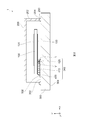
- FIG. 1 is an exploded perspective view of a piezoelectric vibrator according to an embodiment of the present invention.
- 2 is a cross-sectional view taken along line II-II in FIG.
- FIG. 3 is a diagram schematically showing a top view of the conductive holding member.
- the conductive holding member 342 includes an adhesive 400, a plurality of spherical spacers 410, and a plurality of metal particles 420. It is a figure which shows a mode.
- FIG. 4 is a conceptual diagram for explaining the relationship between the size of the spherical spacer and the size of the metal particles, and specifically shows a state in which one metal particle enters a gap formed by three spherical spacers.
- FIG. 5 is a conceptual diagram for explaining the relationship between the size of the spherical spacer and the size of the metal particles, and specifically shows a state in which three metal particles enter a gap formed by the three spherical spacers. It is.
- FIG. 1 is an exploded perspective view of a piezoelectric vibrator according to an embodiment of the present invention
- FIG. 2 is a sectional view taken along line II-II in FIG.
- the piezoelectric vibrator 1 includes a piezoelectric vibration element 100 (Piezoelectric Resonator), a lid member 200, and a substrate 300.
- the lid member 200 and the substrate 300 are part of the structure of a holder (case or package) for housing the piezoelectric vibration element 100.
- the piezoelectric vibration element 100 includes a piezoelectric substrate 110 and excitation electrodes (Excitation Electrodes) 120 and 130 (hereinafter referred to as “first excitation electrode 120” and “second excitation electrode 130”) provided on the front and back surfaces of the piezoelectric substrate 110, respectively. Also).
- excitation electrodes 120 and 130 hereinafter referred to as “first excitation electrode 120” and “second excitation electrode 130”
- the piezoelectric substrate 110 is formed from a predetermined piezoelectric material, and the material is not particularly limited.
- the piezoelectric substrate 110 is formed from an artificial crystal having a predetermined crystal orientation (Synthetic Quartz Crystal).
- the piezoelectric substrate 110 is, for example, an AT-cut crystal piece (Quartz Crystal Element).
- the AT-cut crystal piece is 35 degrees 15 minutes in the direction from the Y axis to the Z axis around the X axis among the X, Y, and Z axes that are the crystal axes of the artificial quartz.
- the piezoelectric substrate 110 which is an AT-cut crystal piece has a long side extending along the X axis, a short side extending along the Z ′ axis, and a thickness extending along the Y ′ axis. And has a substantially rectangular shape on the XZ ′ plane.
- a piezoelectric vibration element using an AT-cut crystal piece has high frequency stability over a wide temperature range, and is excellent in aging characteristics.
- a piezoelectric vibration element using an AT-cut crystal piece that is, a quartz vibration element
- the piezoelectric substrate is not limited to the above configuration, and for example, a rectangular AT-cut quartz piece having a long side extending along the Z ′ axis and a short side extending along the X axis is applied. May be.
- a crystal piece with a cut other than the AT cut such as a BT cut may be used.
- the material of the piezoelectric substrate is not limited to quartz, and for example, a piezoelectric ceramic such as PZT or other piezoelectric material such as zinc oxide may be used.
- the piezoelectric vibration element may be, for example, a MEMS (Micro Electro Mechanical Systems), and specifically, Si-MEMS in which a MEMS is formed on a silicon substrate may be used. Furthermore, the piezoelectric vibration element may be a piezoelectric MEMS using a predetermined piezoelectric material such as AlN, LiTaO 3 , LiNbO 3 , or PZT.
- the first excitation electrode 120 is formed on the first main surface 112 of the piezoelectric substrate 110, and the second excitation electrode 130 is formed on the second main surface 114 of the piezoelectric substrate 110.
- the first excitation electrode 120 and the second excitation electrode 130 are a pair of electrodes, and are disposed so as to substantially overlap each other when the XZ ′ plane is viewed in plan.
- the piezoelectric substrate 110 has a connection electrode 124 electrically connected to the first excitation electrode 120 via the extraction electrode 122, and a connection electrode 134 electrically connected to the second excitation electrode 130 via the extraction electrode 132. And are formed. Specifically, the extraction electrode 122 is extracted from the first excitation electrode 120 toward the short side of the X-axis negative direction side on the first main surface 112 and further passes through the side surface of the piezoelectric substrate 110 on the Z′-axis positive direction side. Thus, the connection electrode 124 formed on the second main surface 114 is connected.
- the extraction electrode 132 is extracted from the second excitation electrode 130 toward the X-axis negative direction side short side on the second main surface 114 and connected to the connection electrode 134 formed on the second main surface 114.
- the connection electrodes 124 and 134 are disposed along the short side of the X-axis negative direction, and are electrically held and mechanically held by the substrate 300 via the conductive holding members 340 and 342 (holding portions).
- the arrangement and pattern shape of the connection electrodes 124 and 134 and the extraction electrodes 122 and 132 are not limited, and may be changed as appropriate in consideration of electrical connection with other members.
- Each of the electrodes including the first excitation electrode 120 and the second excitation electrode 130 has, for example, a chromium (Cr) layer formed on the surface of the piezoelectric substrate 110 as a base to increase the bonding force, and a gold layer on the surface of the chromium layer.
- An (Au) layer is formed.
- the material is not limited.
- the lid member 200 has a recess that opens to face the first main surface 302 of the substrate 300.
- the lid member 200 is provided with a side wall portion 202 formed so as to rise from the bottom surface of the recess over the entire circumference of the opening.
- the side wall portion 202 is an end surface 204 facing the first main surface 302 of the substrate 300. have.
- the end surface 204 is bonded to the first main surface 302 of the substrate 300 via the bonding material 250.
- the lid member 200 may have any shape that can accommodate the piezoelectric vibration element 100 in the internal space when bonded to the substrate 300, and the shape is not particularly limited.
- the material of the lid member 200 is not particularly limited, but may be made of a conductive material such as metal.
- a shield function can be added by electrically connecting the lid member 200 to the ground potential.
- the lid member 200 may be made of an alloy (for example, 42 alloy) containing iron (Fe) and nickel (Ni).
- a surface layer such as a gold (Au) layer may be further formed on the surface of the lid member 200. By forming a gold layer on the surface, it is possible to prevent the lid member 200 from being oxidized.
- the lid member 200 may be an insulating material or a composite structure of a conductive material and an insulating material.
- the substrate 300 holds the piezoelectric vibration element 100.
- the piezoelectric vibration element 100 is held on the first main surface 302 of the substrate 300 through the conductive holding members 340 and 342 so as to be able to be excited.
- the substrate 300 has a long side extending along the X axis, a short side extending along the Z ′ axis, and a side in the thickness direction extending along the Y ′ axis, and is substantially rectangular on the XZ ′ plane. It has a shape.
- the substrate 300 is made of, for example, a single layer of insulating ceramic. As another embodiment, the substrate 300 may be formed by stacking and firing a plurality of insulating ceramic sheets.
- the substrate 300 is preferably made of a heat resistant material.
- the substrate 300 may have a flat plate shape as shown in FIG. 1, or may have a concave shape opened in a direction facing the lid member 200.
- connection electrodes 320 and 322, corner electrodes 324 and 326, and extraction electrodes 320a and 322a are formed on the first main surface 302, and side electrodes 330, 332, 334, and 336 are formed on the side surfaces.
- External electrodes 360, 362, 364, 366 are formed on the main surface 304.
- connection electrodes 320 and 322 are formed on the first main surface 302 of the substrate 300 along the short side on the X axis negative direction side and spaced from the short side.
- the connection electrode 320 is connected to the connection electrode 124 of the piezoelectric vibration element 100 via the conductive holding member 340
- the connection electrode 322 is connected to the connection electrode 134 of the piezoelectric vibration element 100 via the conductive holding member 342.
- the material of the connection electrodes 320 and 322 is not particularly limited.
- the connection electrodes 320 and 322 are formed of a laminate of molybdenum (Mo), nickel (Ni), and gold (Au).
- the conductive holding members 340 and 342 are formed by, for example, thermosetting an adhesive. Details of the configuration of the conductive holding members 340 and 342 will be described later.
- the extraction electrode 320 a is extracted from the connection electrode 320 toward the side electrode 330 provided at one corner of the substrate 300.
- the extraction electrode 322a is extracted along the X-axis direction from the connection electrode 322 toward the side electrode 332 provided at the corner of the substrate 300 at the diagonal position of the side electrode 330.
- corner electrodes 324 and 326 are formed in the remaining corners (corners other than the corners where the extraction electrodes 320a and 322a electrically connected to the connection electrodes 320 and 322 are disposed). .
- the corner electrodes 324 and 326 are electrodes that are not electrically connected to either the first excitation electrode 120 or the second excitation electrode 130.
- the plurality of side surface electrodes 330, 332, 334, and 336 are formed on the side surfaces near the respective corners of the substrate 300. Further, the plurality of external electrodes 360, 362, 364, 366 are formed in the vicinity of each corner on the second main surface 304 of the substrate 300. Specifically, the side electrode 330 and the external electrode 360 are arranged at corners on the X axis negative direction and the Z ′ axis positive direction side, and the side electrode 332 and the external electrode 362 are on the X axis positive direction and the Z ′ axis negative direction side.
- the side electrode 334 and the external electrode 364 are arranged at the corners on the X axis positive direction and the Z ′ axis positive direction side, and the side electrode 336 and the external electrode 366 are arranged on the X axis negative direction and the Z ′ axis negative direction. It is arranged at the corner on the direction side.
- Side electrodes 330, 332, 334, and 336 are provided to electrically connect the electrodes on the first main surface 302 and the second main surface 304.
- a corner portion of the substrate 300 has a cut-out side surface formed by cutting a part of the corner portion into a cylindrical curved surface shape (also referred to as a castellation shape).
- Side electrodes 330, 332, 334, and 336 are formed on the side surfaces.
- the shape of the corner portion of the substrate 300 is not limited to this, and the shape of the cutout may be a flat shape, or may be a rectangular shape having no cutout and having four corners at right angles in plan view. There may be.
- External electrodes 360, 362, 364, and 366 are electrodes for electrical connection with a mounting board (not shown).
- the external electrodes 360, 362, 364, and 366 are electrically connected to side electrodes 330, 332, 334, and 336 formed on the side surfaces of the corresponding corners, respectively.
- the external electrodes 360, 362, 364, and 366 can be electrically connected to the electrodes on the first main surface 302 side of the substrate 300 via the side electrodes 330, 332, 334, and 336.
- the external electrode 360 is electrically connected to the first excitation electrode 120 via the side electrode 330, the extraction electrode 320a, the connection electrode 320, and the conductive holding member 340.
- the external electrode 362 is electrically connected to the second excitation electrode 130 via the side electrode 332, the extraction electrode 322a, the connection electrode 322, and the conductive holding member 342. That is, the external electrodes 360 and 362 are input / output terminals that are electrically connected to the first excitation electrode 120 or the second excitation electrode 130.
- the remaining external electrodes 364 and 366 are dummy electrodes that are not electrically connected to the first excitation electrode 120 or the second excitation electrode 130 of the piezoelectric vibration element 100.
- the external electrodes 364 and 366 can be formed at all corners, so that the process of electrically connecting the piezoelectric vibrator 1 to another member is facilitated.
- the external electrodes 364 and 366 may function as a grounding electrode to which a ground potential is supplied.
- the lid member 200 when the lid member 200 is made of a conductive material, the lid member 200 can be provided with a shielding function by electrically connecting the lid member 200 to the external electrodes 364 and 366 that are grounding electrodes.
- each structure of the connection electrode, the corner electrode, the extraction electrode, the side electrode, and the external electrode formed on the substrate 300 is not limited to the above-described example, and various modifications can be applied.
- the number of external electrodes is not limited to four.
- only two input / output terminals arranged diagonally may be provided.
- the side electrodes are not limited to those arranged at the corners, and may be formed on any side surface of the substrate 300 excluding the corners. In this case, as already described, a cut-out side surface in which a part of the side surface is cut into a cylindrical curved surface may be formed, and a side electrode may be formed on the side surface excluding the corners.
- corner electrodes 324 and 326, the side surface electrodes 334 and 336, and the external electrodes 364 and 366 may not be formed.
- a through hole penetrating from the first main surface 302 to the second main surface 304 is formed in the substrate 300, and electrical conduction is made from the connection electrode formed on the first main surface 302 to the second main surface 304 by this through hole. You may plan.
- the bonding material 250 is provided over the entire circumferences of the lid member 200 and the substrate 300, and bonds the end surface 204 of the side wall portion 202 of the lid member 200 and the first main surface 302 of the substrate 300.
- the material of the bonding material 250 is not limited, but may be, for example, a gold (Au) -tin (Sn) eutectic alloy.
- the piezoelectric vibration element 100 is hermetically sealed in an internal space (cavity) surrounded by the concave portion of the lid member 200 and the substrate 300.
- the pressure in the internal space is a vacuum state lower than the atmospheric pressure, thereby reducing a change with time due to oxidation of the first excitation electrode 120 and the second excitation electrode 130.
- the piezoelectric vibrator 1 an alternating electric field is applied between the pair of first excitation electrode 120 and second excitation electrode 130 in the piezoelectric vibration element 100 via the external electrodes 360 and 362 of the substrate 300.
- FIG. 3 is a diagram schematically showing a top view of the conductive holding member.
- the conductive holding member 342 includes an adhesive 400, a plurality of spherical spacers 410, and a plurality of metal particles 420. It is a figure which shows a mode. 3 schematically shows the conductive holding member 342 provided on the connection electrode 322 in a plan view of the substrate 300 (that is, a plan view of the XZ ′ plane). The lid member 200 and the piezoelectric vibration element are shown in FIG. 100 is omitted. In the following description, since the conductive holding member 340 is the same as the conductive holding member 342, detailed description thereof is omitted.
- the conductive holding member 342 includes an adhesive (binder) 400, a plurality of spherical spacers 410, and a plurality of metal particles 420.
- the adhesive 400 contains, for example, a resin as a main component.
- Each of the plurality of spherical spacers 410 is mainly composed of a resin such as rubber having elasticity or plastic such as silicone resin.
- a silicone resin is used for the plurality of spherical spacers 410.
- the adhesive 400 and the spherical spacer 410 may be distinguished from each other by using different types of resins, for example.
- Each of the plurality of spherical spacers 410 has a spherical shape, for example.
- the spherical shape is not limited to a spherical shape, and includes an elliptical shape, a spherical shape or a shape obtained by slightly deforming an elliptical shape, and the like.
- the plurality of spherical spacers 410 are not covered with metal, and a silicone resin material that is an insulator is exposed on the surface.
- Such a spherical spacer 410 has a lower Young's modulus and a lower acoustic impedance than a spherical spacer coated with metal.
- Each of the plurality of spherical spacers 410 has a particle diameter V, and an average value of the particle diameters V is an average particle diameter V ave .
- the particle diameter V of the spherical spacer is an equivalent circle diameter obtained from the cross-sectional area of the spherical spacer in an arbitrary cross-sectional view.
- the cross-sectional view is, for example, a cross-sectional image of the conductive holding member acquired at a magnification of 10,000 times with a scanning ion microscope using a focused ion beam (FIB).
- the average particle diameter V ave is the particle diameter of a total of 100 spherical spacers selected from 10 particles estimated to have the maximum length in each of the cross-sectional images of 10 conductive holding members having different cross sections. Average value.
- the spherical spacer before adding to an electroconductive holding member can be measured, you may measure an average particle diameter using the particle size distribution measuring apparatus of a laser diffraction and a scattering method.
- the definitions of the particle diameter and the average particle diameter are the same in the particle diameter and average particle diameter of metal particles described later.
- the particle size V of the spherical spacer 410 is such that the surface of the second excitation electrode 130 formed on the second main surface 114 of the piezoelectric vibration element 100 and the surface of the connection electrode 322 formed on the first main surface 302 of the substrate 300.
- the distance L is equal to or smaller than the distance L (that is, V ⁇ L is satisfied) (see FIG. 2).
- the piezoelectric vibration element 100 is placed on the surface of the connection electrode 322 with a plurality of spherical spacers 410 interposed therebetween.
- the piezoelectric vibration element 100 responds to the particle diameter V of the spherical spacer from the surface of the connection electrode 322. It will be held at intervals. Specifically, for example, when the spherical spacers 410 are stacked one stage in the Y′-axis direction as shown in FIG. 2, the piezoelectric vibrating element 100 has an interval corresponding to the particle diameter V of the spherical spacers 410 (for example, 5 About 6 ⁇ m).
- the piezoelectric vibration element 100 has an interval (for example, about 10 to 11 ⁇ m) corresponding to about twice the particle diameter V of the spherical spacers 410.
- the spherical spacer 410 may be slightly deformed by being sandwiched between the connection electrode 322 and the piezoelectric vibration element 100, and the length in the Y-axis direction may be shorter than the particle diameter V before bonding. In this way, the distance between the second main surface 114 of the piezoelectric vibration element 100 and the first main surface 302 of the substrate 300 is kept constant, and parasitics generated between the electrodes formed on both the main surfaces. The capacity can be kept constant.
- the plurality of spherical spacers 410 are provided, for example, on the connection electrode 322 (see FIG. 3).
- “being spread” is a state in which the surfaces of adjacent spherical spacers among the plurality of spherical spacers 410 are arranged so as to contact each other, as shown in FIG. 3.
- a plurality of spherical spacer groups constituted by three spherical spacers 410 a, 410 b, 410 c adjacent to each other are arranged on the first main surface of the substrate.
- a gap is formed in a region surrounded by three spherical spacers 410a to 410c adjacent to each other.
- the spherical spacer groups are stacked in a plurality of stages in the Y′-axis direction, gaps similar to the gaps are formed between the spherical spacer groups stacked in the Y′-axis direction.
- Each of the plurality of metal particles 420 is a particle formed by bonding a plurality of metal atoms.
- the material of the plurality of metal particles 420 is not particularly limited, for example, silver (Ag) or the like is a main component.
- the plurality of metal particles 420 are cured while being in contact with each other between the adhesives 400, whereby the conductive holding member 342 becomes an adhesive that functions as a holding member while having conductivity.
- Each of the plurality of metal particles 420 has a particle diameter W, and an average value of the particle diameters W is an average particle diameter W ave .
- variation (namely, particle diameter distribution) of the particle diameter of the some metal particle 420 can approximate the normal distribution function of standard deviation (sigma), for example.
- Each of the plurality of metal particles 420 is disposed so as to enter a gap formed by the plurality of spherical spacers 410 spread on the connection electrode 322, and is in contact with each other in the Y′-axis direction. That is, the particle diameter W of the metal particles 420 is smaller than the gap formed by the three spherical spacers 410a to 410c constituting the spherical spacer group. This point will be described with reference to FIGS. In FIGS. 4 and 5, description will be made assuming that both the spherical spacer and the metal particle are spheres circumscribing each other.
- FIG. 4 is a conceptual diagram for explaining the relationship between the size of the spherical spacer and the size of the metal particles. Specifically, the relationship between the three spherical spacers arranged next to each other on the first main surface 302 of the substrate 300 is shown. It is a figure which shows a mode that one metal particle enters into the formed clearance gap.
- FIG. 5 is a conceptual diagram for explaining the relationship between the size of the spherical spacer and the size of the metal particles. Specifically, the state in which the three metal particles enter the gap formed by the three spherical spacers.
- FIG. 4 and 5 are cross sections parallel to the XZ ′ plane when the plurality of spherical spacers are spread evenly as shown in FIG.
- a cross section of the height is schematically shown. That is, at the height, the gap formed by the plurality of spherical spacers is the narrowest.
- the radius of the great circle 10a, 10b, 10c of the sphere corresponding to the spherical spacer is R (corresponding to V / 2)
- the radius of the small circle 20a, 20b, 20c of the sphere corresponding to the metal particle is r ( Equivalent to W / 2).
- FIG. 4 is a conceptual diagram showing a case where one metal particle enters a gap formed by three spherical spacers in a certain spherical spacer group.
- the center of the great circle 10a is O
- the center of the small circle 20a is P
- the contact point between the great circle 10a and the great circle 10b is Q
- r ⁇ (2 / ⁇ 3) ⁇ 1 ⁇ ⁇ R (1)
- some of the plurality of metal particles having the average particle diameter W ave may enter the gap formed by the plurality of spherical spacers having the average particle diameter V ave. it can.
- the metal particles having a particle diameter W smaller than the average particle diameter W ave For example, the ratio is about half of the entire metal particles contained in the conductive holding member.
- W ave ⁇ (2 / ⁇ 3) ⁇ 1 ⁇ ⁇ V ave ( ⁇ 0.15 ⁇ V ave ) (3)
- FIG. 5 is a conceptual diagram showing a case where three metal particles enter a gap formed by three spherical spacers in a certain spherical spacer group.
- the center of the great circle 10a is O
- the center of the small circle 20a is P
- the contact point of the great circle 10a and the great circle 10b is Q
- the contact point of the great circle 10a and the small circle 20a is S
- the contact point of the small circle 20a and the small circle 20c Is T
- the intersection of the straight line OT and the straight line QP U
- the line segment OQ R
- the line segment OP (R + r)
- the line segment PT r.
- the line segment OT ⁇ ⁇ (R + r) 2 ⁇ r 2 ⁇ from the three square theorem.
- a part of the plurality of metal particles having an average particle diameter W ave (for example, about half of the whole metal particles included in the conductive holding member) is three. At the same time, it can enter the gap formed by the three spherical spacers having an average particle diameter V ave .
- W ave ⁇ (5-2 ⁇ 6) ⁇ V ave ( ⁇ 0.10 ⁇ V ave ) (9)
- the spherical spacer is mixed. Even if it is, the electroconductivity of a conductive holding member can be maintained favorable. Therefore, in the piezoelectric vibrator 1, the conductivity of the conductive holding member (holding portion) that holds the piezoelectric vibration element is improved while keeping the distance between the piezoelectric vibration element 100 and the main surface of the substrate 300 constant. In addition, since it is not necessary to coat the spherical spacer with metal, the manufacturing cost is lower than that of the structure coated with metal.
- the Young's modulus of the conductive holding members 340 and 342 is smaller and the acoustic impedance is lower than that of the conventional piezoelectric vibrator disclosed in Patent Document 1, for example. .
- the difference in acoustic impedance between the piezoelectric vibration element 100 and the substrate 300 having a relatively high acoustic impedance and the conductive holding member having a relatively low acoustic impedance increases.
- the greater the difference in acoustic impedance of each object the greater the reflected wave of vibration at the boundary surface between the objects, and the reduced the transmitted wave.
- the reflected wave at the boundary surface between the piezoelectric vibration element 100 and the conductive holding members 340 and 342 increases, and the transmitted wave to the substrate 300 decreases. Accordingly, vibration leaking from the piezoelectric vibration element 100 to the substrate 300 via the conductive holding members 340 and 342 is reduced, and a decrease in the CI (Crystal Impedance) value of the piezoelectric vibrator 1 is suppressed.
- the average particle diameter W ave of the plurality of metal particles may satisfy the following formula (10).
- at least six metal particles can simultaneously enter the gap formed by the three spherical spacers. Therefore, since the generation of powder bridges of the metal particles is suppressed, the metal particles are more likely to enter the gap, and the conductivity of the conductive holding member is improved.
- W ave ⁇ [ ⁇ (2 / ⁇ 3) ⁇ 1 ⁇ / 6] ⁇ V ave ( ⁇ 0.03 ⁇ V ave ) (10)
- the piezoelectric vibration element 100 has one end fixed by conductive holding members 340 and 342 and the other end is free. It may be fixed to the substrate 300 at both ends. That is, one of the connection electrodes 320, 322 is formed on the X axis positive direction side and the other is formed on the X axis negative direction side. Also good.
- FIG. 2 shows an example in which one spherical spacer is stacked in the height direction (Y′-axis direction), but the number of the spherical spacers is not limited to this, and two steps in the height direction are provided. The above may be stacked.
- the metal particles in order to simultaneously enter six metal particles into the gap formed by the three spherical spacers, it is necessary to make the metal particles relatively smaller than the spherical spacers.
- the proportion of the metal particles in the conductive holding member increases.
- the acoustic impedance of the conductive holding member is increased.
- the difference in acoustic impedance between the conductive holding member and the piezoelectric vibration element 100 and the substrate 300 tends to be small.
- the number of metal particles entering the gap formed by the three spherical spacers having an average particle diameter V ave is, for example, up to six.
- the average particle diameter W ave preferably satisfies the following formula (11). W ave ⁇ [ ⁇ (2 / ⁇ 3) ⁇ 1 ⁇ / 6] ⁇ V ave ( ⁇ 0.03 ⁇ V ave ) (11)
- the piezoelectric vibrator 1 may not include the lid member 200.
- the conductive holding members 340 and 342 include a plurality of metal particles 420 and a plurality of spherical spacers 410 that hold the piezoelectric vibration element 100 at a predetermined interval from the first main surface 302 of the substrate 300.
- the average particle diameter of the spherical spacer 410 is V ave and the average particle diameter of the metal particles 420 is W ave .
- the relationship is W ave ⁇ (2 / ⁇ 3) ⁇ 1 ⁇ ⁇ V ave .
- the metal particles 420 sufficiently enter the gap formed by the spherical spacer 410, so that the conductivity of the conductive holding members 340 and 342 is improved. Moreover, since it is not necessary to coat the spherical spacer with metal, the manufacturing cost is low. Further, since spherical spacers that are not covered with metal are used, the Young's modulus of the conductive holding members 340 and 342 is small, and the acoustic impedance is low. Thereby, vibration leaking from the piezoelectric vibration element 100 to the substrate 300 via the conductive holding members 340 and 342 is reduced, and a decrease in the CI value of the piezoelectric vibrator 1 is suppressed.
- the piezoelectric vibrator 1 When the particle size distribution of the metal particles 420 is approximated to a normal distribution function with a standard deviation ⁇ , the piezoelectric vibrator 1 further has a relationship of W ave + 2 ⁇ ⁇ (2 / ⁇ 3) ⁇ 1 ⁇ ⁇ V ave. You may do it. Thereby, most (for example, about 95% of the total) of the plurality of metal particles 420 can enter the gap formed by the spherical spacer 410. Therefore, the conductivity of the conductive holding members 340 and 342 is further improved.
- the piezoelectric vibrator 1 may further have a relationship of W ave ⁇ (5-2 ⁇ 6) ⁇ V ave .
- the metal particles 420 can easily enter the gap formed by the spherical spacer 410. Therefore, the conductivity of the conductive holding members 340 and 342 is further improved.
- the material of the spherical spacer 410 is not particularly limited, but for example, a resin may be the main component.
- the spherical spacer 410 may have an insulating surface, for example. Thereby, the spherical spacer 410 has a lower acoustic impedance than the spherical spacer coated with metal. Therefore, vibration leaking from the piezoelectric vibration element 100 to the substrate 300 via the conductive holding members 340 and 342 is reduced, and a decrease in the CI value of the piezoelectric vibrator 1 is suppressed.
- the material of the metal particles 420 is not particularly limited, but for example, silver may be the main component.
- the plurality of spherical spacers 410 are arranged on the first main surface 302 of the substrate 300 and have a spherical spacer set constituted by three spherical spacers 410a to 410c adjacent to each other.
- a plurality of particles that pass through a gap surrounded by the two spherical spacers 410a to 410c and are in contact with each other in the normal direction of the first main surface 302 may be included.
- the three spherical spacers 410a to 410c may be in contact with each other.
- a plurality of spherical spacer groups may be arranged on the first main surface 302 of the substrate 300.
- the piezoelectric vibrator 1 further includes a lid member 200 that is bonded to the substrate 300 and accommodates the piezoelectric vibration element 100. Thereby, the piezoelectric vibration element 100 can be accommodated in the internal space.
- each embodiment described above is for facilitating understanding of the present invention, and is not intended to limit the present invention.
- the present invention can be changed / improved without departing from the spirit thereof, and the present invention includes equivalents thereof. That is, those in which the person skilled in the art appropriately changes the design of each embodiment is also included in the scope of the present invention as long as the features of the present invention are included.
- each element included in each embodiment and its arrangement, material, condition, shape, size, and the like are not limited to those illustrated, and can be changed as appropriate.
- each element included in each embodiment can be combined as much as technically possible, and combinations thereof are included in the scope of the present invention as long as they include the features of the present invention.
- Piezoelectric vibrator 100 Piezoelectric vibration element 110 Piezoelectric substrate 120,130 Excitation electrode 122,132 Extraction electrode 124,134 Connection electrode 200 Lid member 250 Bonding material 300 Substrate 320,322 Connection electrode 320a, 322a Extraction electrode 324,326 Corner electrode 330 , 332, 334, 336 Side electrode 340, 342 Conductive holding member 360, 362, 364, 366 External electrode 400 Adhesive 410 Spherical spacer 420 Metal particles 10a, 10b, 10c Large circle 20a, 20b, 20c Small circle
Landscapes
- Physics & Mathematics (AREA)
- Acoustics & Sound (AREA)
- Piezo-Electric Or Mechanical Vibrators, Or Delay Or Filter Circuits (AREA)
Abstract
圧電振動子(1)は、圧電振動素子(100)と、対向する第1及び第2主面を有する基板(300)と、圧電振動素子を基板の第1主面上に保持する導電性保持部材(340,342)と、を備え、導電性保持部材は、複数の金属粒子(420)と、圧電振動素子を基板の第1主面から所定の間隔をあけて保持する複数の球状スペーサ(410)と、を含み、球状スペーサの平均粒子径をVaveとし、金属粒子の平均粒子径をWaveとした場合、Wave<{(2/√3)-1}×Vaveの関係を有する。
Description
本発明は、圧電振動子に関し、特に、圧電振動素子が導電性保持部材によって基板上に保持された圧電振動子に関する。
圧電振動子の一態様として、基板の主面に圧電振動素子が載置される構造が知られている。このような構造においては、圧電振動素子に形成された電極と基板に形成された電極との間に発生する寄生容量のばらつきが抑制されるよう、圧電振動素子と基板の主面との距離が一定に保たれることが好ましい。例えば、特許文献1には、圧電振動片を保持する保持部となる接着剤に球状スペーサが混入され、当該球状スペーサの直径により基板と圧電振動片の隙間が確保される圧電デバイスが開示されている。当該接着剤には、球状スペーサの直径の1/4以下である外形寸法の金属粒子が混入されており、電気的導通が図られている。
しかしながら、特許文献1に開示されるような圧電デバイスでは、接着剤において金属粒子が球状スペーサによって形成された隙間に充分に入り込まず、接着剤の導電性が低下する問題がある。
本発明はこのような事情に鑑みてなされたものであり、圧電振動素子と基板主面との距離を一定に保ちつつ、圧電振動素子の保持部の導電性が向上する圧電振動子を提供することを目的とする。
本発明の一側面に係る圧電振動子は、圧電振動素子と、対向する第1及び第2主面を有する基板と、圧電振動素子を基板の第1主面上に保持する導電性保持部材と、を備え、導電性保持部材は、複数の金属粒子と、圧電振動素子を基板の第1主面から所定の間隔をあけて保持する複数の球状スペーサと、を含み、球状スペーサの平均粒子径をVaveとし、金属粒子の平均粒子径をWaveとした場合、Wave<{(2/√3)-1}×Vaveの関係を有する。
上記構成によれば、圧電振動素子の保持部において、金属粒子が球状スペーサによって形成された隙間に充分に入り込むことができる。従って、当該保持部の導電性が向上する。
本発明によれば、圧電振動素子と基板主面との距離を一定に保ちつつ、圧電振動素子の保持部の導電性が向上する圧電振動子を提供することができる。
以下に本発明の実施形態を説明する。以下の図面の記載において、同一又は類似の構成要素は同一又は類似の符号で表している。図面は例示であり、各部の寸法や形状は模式的なものであり、本願発明の技術的範囲を当該実施形態に限定して解するべきではない。
図1及び図2を参照しつつ、本発明の一実施形態に係る圧電振動子1を説明する。図1は、本発明の一実施形態に係る圧電振動子の分解斜視図であり、図2は、図1のII-II線断面図である。
図1に示されるように、本実施形態に係る圧電振動子1は、圧電振動素子100(Piezoelectric Resonator)と、蓋部材200と、基板300と、を備える。蓋部材200及び基板300は、圧電振動素子100を収容するための保持器(ケース又はパッケージ)の構成の一部である。
圧電振動素子100は、圧電基板110と、圧電基板110の表裏面にそれぞれ設けられた励振電極(Excitation Electrodes)120,130(以下では、「第1励振電極120」及び「第2励振電極130」ともいう。)と、を含む。
圧電基板110は、所定の圧電材料から形成され、その材料は特に限定されるものではない。図1に示される例では、圧電基板110は、所定の結晶方位を有する人工水晶(Synthetic Quartz Crystal)から形成されている。圧電基板110は、例えば、ATカットされた水晶片(Quartz Crystal Element)である。ATカットされた水晶片は、人工水晶の結晶軸であるX軸、Y軸、Z軸のうち、Y軸及びZ軸をX軸の周りにY軸からZ軸の方向に35度15分±1分30秒分回転させた軸をそれぞれY´軸及びZ´軸とした場合、X軸及びZ´軸によって特定される面(以下、「XZ´面」と呼ぶ。他の軸によって特定される面についても同様である。)と平行な面を主面として切り出されたものである。図1に示される例では、ATカットされた水晶片である圧電基板110は、X軸に沿って延びる長辺と、Z´軸に沿って延びる短辺と、Y´軸に沿って延びる厚み方向の辺と、を有しており、XZ´面において略矩形状をなしている。ATカットされた水晶片を用いた圧電振動素子は、広い温度範囲で高い周波数安定性を有し、また、経時変化特性にも優れている。また、ATカットされた水晶片を用いた圧電振動素子(すなわち、水晶振動素子(Quartz Crystal Resonator))は、主要振動として厚みすべり振動モード(Thickness Shear Mode)を含む。以下、ATカットの軸方向を基準として圧電振動子1の各構成を説明する。
なお、圧電基板は上記構成に限定されるものではなく、例えば、Z´軸に沿って延びる長辺と、X軸に沿って延びる短辺とを有する矩形状のATカットされた水晶片を適用してもよい。あるいは、主要振動が厚みすべり振動モードを含んでいれば、例えば、BTカットなどのATカット以外のカットの水晶片であってもよい。また、圧電基板の材料は水晶に限定されるものではなく、例えば、PZTなどの圧電セラミックや酸化亜鉛などのその他の圧電材料を用いてもよい。また、圧電振動素子は、例えばMEMS(Micro Electro Mechanical Systems)であってもよく、具体的には、シリコン基板にMEMSを形成したSi-MEMSを用いてもよい。さらに、圧電振動素子は、AlN、LiTaO3、LiNbO3、PZTなどの所定の圧電材料を用いた圧電MEMSであってもよい。
第1励振電極120は、圧電基板110の第1主面112に形成され、第2励振電極130は、圧電基板110の第2主面114に形成されている。第1励振電極120及び第2励振電極130は、一対の電極であり、XZ´面を平面視した場合に略全体が重なり合うように配置されている。
圧電基板110には、第1励振電極120に引出電極122を介して電気的に接続された接続電極124と、第2励振電極130に引出電極132を介して電気的に接続された接続電極134と、が形成される。具体的には、引出電極122は、第1主面112において第1励振電極120からX軸負方向側短辺に向かって引き出され、さらに圧電基板110のZ´軸正方向側の側面を通って、第2主面114に形成された接続電極124に接続される。他方、引出電極132は、第2主面114において第2励振電極130からX軸負方向側短辺に向かって引き出され、第2主面114に形成された接続電極134に接続される。接続電極124,134はX軸負方向側短辺に沿って配置され、導電性保持部材340,342(保持部)を介して基板300に電気的導通を図るとともに機械的に保持される。なお、接続電極124,134及び引出電極122,132の配置やパターン形状は限定されるものではなく、他の部材との電気的接続を考慮して適宜変更されてもよい。
第1励振電極120及び第2励振電極130を含む上記各電極は、例えば、圧電基板110の表面に接合力を高めるためクロム(Cr)層が下地として形成されており、クロム層の表面に金(Au)層が形成されている。なお、その材料は限定されるものではない。
図2に示されるように、蓋部材200は、基板300の第1主面302に対向して開口した凹部を有している。蓋部材200は、開口の全周に亘って、凹部の底面から立ち上がるように形成された側壁部202が設けられており、側壁部202は、基板300の第1主面302に対向する端面204を有している。端面204は、接合材250を介して基板300の第1主面302と接合される。なお、蓋部材200は基板300に接合されたときに圧電振動素子100を内部空間に収容することができる形状であればよく、その形状は特に限定されるものではない。蓋部材200の材質は特に限定されるものではないが、例えば金属などの導電性材料で構成されていてもよい。これによれば、蓋部材200を接地電位に電気的に接続させることによりシールド機能を付加することができる。蓋部材200が金属によって形成される場合、例えば、鉄(Fe)及びニッケル(Ni)を含む合金(例えば42アロイ)で形成されてもよい。あるいは、蓋部材200の表面にさらに金(Au)層などの表面層が形成されてもよい。表面に金層が形成されることにより、蓋部材200の酸化防止を図ることができる。あるいは、蓋部材200は、絶縁材料又は導電材料及び絶縁材料の複合構造であってもよい。
図1に戻り、基板300は、圧電振動素子100を保持するものである。図1に示される例では、圧電振動素子100が、導電性保持部材340,342を介して基板300の第1主面302上に励振可能に保持されている。
基板300は、X軸に沿って延びる長辺と、Z´軸に沿って延びる短辺と、Y´軸に沿って延びる厚み方向の辺と、を有しており、XZ´面において略矩形状をなしている。基板300は、例えば単層の絶縁性セラミックで形成されている。別の実施形態として、基板300は、複数の絶縁性セラミックシートを積層して焼成することによって形成されてもよい。基板300は耐熱性材料から構成されることが好ましい。なお、基板300は、図1に示されるように平板状をなしていてもよく、又は蓋部材200に対向する向きに開口した凹状をなしていてもよい。
基板300には、第1主面302に接続電極320,322、コーナー電極324,326、及び引出電極320a,322aが形成され、側面に側面電極330,332,334,336が形成され、第2主面304に外部電極360,362,364,366が形成されている。
接続電極320,322は、基板300の第1主面302上において、X軸負方向側の短辺に沿ってかつ当該短辺から間隔を空けて形成されている。接続電極320は導電性保持部材340を介して圧電振動素子100の接続電極124と接続され、接続電極322は、導電性保持部材342を介して圧電振動素子100の接続電極134と接続される。接続電極320,322の材料は特に限定されないが、例えば、モリブデン(Mo)、ニッケル(Ni)、及び金(Au)の積層により構成される。なお、導電性保持部材340,342は、例えば、接着剤が熱硬化されて形成される。導電性保持部材340,342の構成の詳細については後述する。
引出電極320aは、接続電極320から基板300の1つの角部に設けられた側面電極330に向かって引き出されている。引出電極322aは、接続電極322から基板300における側面電極330の対角位置にある角部に設けられた側面電極332に向かって、X軸方向に沿って引き出されている。
本実施形態においては、残りの角部(接続電極320,322と電気的に接続された引出電極320a,322aが配置された角部以外の角部)にコーナー電極324,326が形成されている。コーナー電極324,326は、第1励振電極120及び第2励振電極130のいずれとも電気的に接続されていない電極である。
複数の側面電極330,332,334,336は、それぞれ、基板300の各角部付近の側面に形成されている。また、複数の外部電極360,362,364,366は、それぞれ、基板300の第2主面304上の各角部付近に形成されている。具体的には、側面電極330及び外部電極360はX軸負方向及びZ´軸正方向側の角部に配置され、側面電極332及び外部電極362はX軸正方向及びZ´軸負方向側の角部に配置され、側面電極334及び外部電極364はX軸正方向及びZ´軸正方向側の角部に配置され、側面電極336及び外部電極366はX軸負方向及びZ´軸負方向側の角部に配置されている。
側面電極330,332,334,336は、第1主面302と第2主面304の各電極を電気的に接続するために設けられている。図1に示される例では、基板300の角部は、その一部が円筒曲面状(キャスタレーション形状とも呼ばれる。)に切断して形成された切り欠き側面をなしており、このような切り欠き側面に側面電極330,332,334,336が形成されている。なお、基板300の角部の形状はこれに限定されるものではなく、切り欠きの形状は平面状であってもよく、又は切り欠きがなく、平面視して四隅が直角である矩形状であってもよい。
外部電極360,362,364,366は、実装基板(図示しない)と電気的に接続するための電極である。外部電極360,362,364,366は、各々、対応する角部の側面に形成された側面電極330,332,334,336に電気的に接続される。これにより、外部電極360,362,364,366は、側面電極330,332,334,336を介して基板300の第1主面302側の電極に電気的に導通可能となる。
具体的には、複数の外部電極のうち、外部電極360は、側面電極330、引出電極320a、接続電極320、及び導電性保持部材340を介して第1励振電極120に電気的に接続され、外部電極362は、側面電極332、引出電極322a、接続電極322、及び導電性保持部材342を介して第2励振電極130に電気的に接続される。すなわち、外部電極360,362は、第1励振電極120又は第2励振電極130と電気的に接続される入出力端子である。
また、残りの外部電極364,366は、圧電振動素子100の第1励振電極120又は第2励振電極130とは電気的に接続されることがないダミー電極である。外部電極364,366を形成することにより、全ての角部に外部電極を形成することができるため、圧電振動子1を他の部材に電気的に接続する処理工程が容易となる。なお、外部電極364,366は、接地電位が供給される接地用電極としての機能を有していてもよい。例えば、蓋部材200が導電性材料からなる場合、蓋部材200を接地用電極である外部電極364,366に電気的に接続することにより、蓋部材200にシールド機能を付与することができる。
なお、基板300に形成される接続電極、コーナー電極、引出電極、側面電極、及び外部電極の各構成は上述の例に限定されるものではなく、様々に変形して適用することができる。例えば、外部電極の個数は4つに限るものではなく、例えば対角上に配置された2つの入出力端子のみであってもよい。また、側面電極は角部に配置されたものに限らず、角部を除く基板300のいずれかの側面に形成されてもよい。この場合、既に説明したとおり、側面の一部を円筒曲面状に切断した切り欠き側面を形成し、角部を除く当該側面に側面電極を形成してもよい。さらに、コーナー電極324,326、側面電極334,336、及び外部電極364,366は形成しなくてもよい。また、基板300に第1主面302から第2主面304へ貫通するスルーホールを形成し、このスルーホールによって第1主面302に形成した接続電極から第2主面304へ電気的導通を図ってもよい。
接合材250は、蓋部材200及び基板300のそれぞれの全周に亘って設けられ、蓋部材200の側壁部202の端面204と基板300の第1主面302とを接合する。接合材250の材料は限定されるものではないが、例えば金(Au)‐錫(Sn)共晶合金としてもよい。蓋部材と基板の接合を金属接合とすることにより、蓋部材が導電性材料で構成されている場合、蓋部材と基板との間の電気的導通を図ることができる。また、封止性を向上させることができる。
蓋部材200及び基板300の両者が接合材250を介して接合されることによって、圧電振動素子100が、蓋部材200の凹部と基板300とによって囲まれた内部空間(キャビティ)に密封封止される。この場合、内部空間の圧力は大気圧力よりも低圧な真空状態であることが好ましく、これにより第1励振電極120及び第2励振電極130の酸化による経時変化などが低減される。
上述の構成により、圧電振動子1においては、基板300の外部電極360,362を介して、圧電振動素子100における一対の第1励振電極120及び第2励振電極130の間に交番電界が印加される。これにより、厚みすべり振動モードを含む振動モードによって圧電基板110が振動し、該振動に伴う共振特性が得られる。
次に、図2及び図3を参照しつつ、導電性保持部材について詳細に説明する。図3は、導電性保持部材の上面図を模式的に示した図であり、具体的には導電性保持部材342に接着剤400、複数の球状スペーサ410及び複数の金属粒子420が含まれた様子を示す図である。なお、図3は、接続電極322上に設けられた導電性保持部材342を基板300の平面視(すなわち、XZ´面の平面視)を模式的に示しており、蓋部材200及び圧電振動素子100が省略されている。また、以下の説明において、導電性保持部材340については導電性保持部材342と同様であるため、詳細な説明は省略する。
図2及び図3に示されるように、導電性保持部材342は、接着剤(バインダー)400、複数の球状スペーサ410及び複数の金属粒子420を含む。なお、接着剤400は、例えば樹脂を主成分とする。
複数の球状スペーサ410の各々は、例えば、弾力性を有するゴム、又は、シリコーン樹脂などのプラスチック等の樹脂を主成分とする。本実施形態では、複数の球状スペーサ410にはシリコーン樹脂が用いられている。接着剤400及び球状スペーサ410がいずれも樹脂を主成分とする場合、接着剤400及び球状スペーサ410は、例えば種類の異なる樹脂が用いられることにより、両者が区別されてもよい。複数の球状スペーサ410の各々は、例えば球形状をなす。なお、球形状とは、球形に限られず、楕円形や、球形又は楕円形が多少変形した形状などを含む。本実施形態においては、複数の球状スペーサ410は金属により被覆されておらず、表面に絶縁体であるシリコーン樹脂材料が露出している。このような球状スペーサ410は、金属により被覆された球状スペーサに比べてヤング率が小さく、音響インピーダンスが低い。
複数の球状スペーサ410は、各々、粒子径Vを有し、当該粒子径Vの平均値を平均粒子径Vaveとする。なお、本明細書において球状スペーサの粒子径Vとは、任意の断面視における球状スペーサの断面面積から求められる円相当径のことである。当該断面視は、例えば、集束イオンビーム(FIB:Focused Ion Beam)を用いた走査イオン顕微鏡による1万倍の倍率にて取得された導電性保持部材の断面画像である。また、平均粒子径Vaveとは、断面の異なる10枚の導電性保持部材の断面画像のそれぞれにおいて、最大長さと推定される10個の粒子を選択した合計100個の球状スペーサの粒子径の平均値である。なお、導電性保持部材に添加する前の球状スペーサが測定できる場合、レーザー回折・散乱法の粒子径分布測定装置を用いて平均粒子径を測定してもよい。この粒子径及び平均粒子径についての定義は、後述する金属粒子の粒子径及び平均粒子径においても同様である。
球状スペーサ410の粒子径Vは、圧電振動素子100の第2主面114に形成された第2励振電極130の表面と、基板300の第1主面302に形成された接続電極322の表面との距離Lとの関係において、当該距離Lと等しいか、又は当該距離Lより小さい(すなわち、V≦Lを満たす)(図2参照)。そして、接続電極322の表面上に、複数の球状スペーサ410を挟んで圧電振動素子100が載置される。これにより、基板300の第1主面302の法線方向、すなわち図2に示されるY´軸方向においては、圧電振動素子100が接続電極322の表面から当該球状スペーサの粒子径Vに応じた間隔をあけて保持されることとなる。具体的には、例えば、図2に示されるように球状スペーサ410がY´軸方向に1段積まれる場合は、圧電振動素子100は球状スペーサ410の粒子径Vに相当する間隔(例えば、5~6μm程度)をあけて保持される。あるいは、例えば、球状スペーサ410がY´軸方向に2段積まれる場合は、圧電振動素子100は球状スペーサ410の粒子径Vの約2倍に相当する間隔(例えば、10~11μm程度)をあけて保持される。なお、球状スペーサ410は、接続電極322と圧電振動素子100との間に挟まれることによってわずかに変形し、Y軸方向の長さが接着前の粒子径Vより短くなっていてもよい。このようにして、圧電振動素子100の第2主面114と基板300の第1主面302との距離が一定に保たれることとなり、当該両主面に形成される電極間に発生する寄生容量の大きさを一定に保つことができる。
また、XZ´面の平面視においては、複数の球状スペーサ410は、例えば接続電極322上に敷き詰められて設けられている(図3参照)。ここで、「敷き詰められる」とは、図3に示されるように、複数の球状スペーサ410のうち隣り合う球状スペーサの表面が互いに接触するように配置された状態である。この時、図3に示されるように、基板の第1主面上には、互いに隣り合う3つの球状スペーサ410a,410b,410cにより構成される球状スペーサ組が複数配置されている。また、互いに隣接する3つの球状スペーサ410a~410cによって囲まれた領域には隙間が形成される。なお、球状スペーサ組がY´軸方向に複数段積まれる場合は、Y´軸方向に積まれた球状スペーサ組の間にも、当該隙間と同様の隙間が形成されることとなる。
複数の金属粒子420の各々は、複数の金属原子が結合してなる粒子である。複数の金属粒子420の材料は特に限定されないが、例えば、銀(Ag)等を主成分とする。複数の金属粒子420が接着剤400の間において互いに接触しつつ硬化されることにより、導電性保持部材342が導電性を備えつつ保持部材として機能する接着剤となる。複数の金属粒子420は、各々、粒子径Wを有し、当該粒子径Wの平均値を平均粒子径Waveとする。なお、複数の金属粒子420の粒子径のばらつき(すなわち、粒子径分布)は、例えば、標準偏差σの正規分布関数に近似できる。複数の金属粒子420の各々は、接続電極322上に敷き詰められた複数の球状スペーサ410によって形成される隙間に入り込むように配置され、Y´軸方向に互いに接触して連なっている。すなわち、金属粒子420の粒子径Wは、球状スペーサ組を構成する3つの球状スペーサ410a~410cによって形成される隙間よりも小さい。この点について、図4及び図5を参照しつつ説明する。なお、図4及び図5では、球状スペーサと金属粒子がいずれもそれぞれに外接する球体であると仮定して説明する。
図4は、球状スペーサの大きさと金属粒子の大きさの関係を説明するための概念図であり、具体的には、基板300の第1主面302上に並ぶ互いに隣り合う3つの球状スペーサによって形成された隙間に1つの金属粒子が入り込む様子を示す図である。また、図5は、球状スペーサの大きさと金属粒子の大きさの関係を説明するための概念図であり、具体的には3つの球状スペーサによって形成された隙間に3つの金属粒子が入り込む様子を示す図である。なお図4及び図5は、図3に示されるように複数の球状スペーサが均等に敷き詰められた場合に、XZ´面と平行な断面であって、隣接する複数の球状スペーサの表面が互いに接する高さの断面を模式的に示している。すなわち、当該高さでは、複数の球状スペーサによって形成される隙間が最も狭くなる。球状スペーサに相当する球の断面の大円10a,10b,10cの半径をR(V/2に相当)とし、金属粒子に相当する球の断面の小円20a,20b,20cの半径をr(W/2に相当)とする。
図4は、ある球状スペーサ組において、3つの球状スペーサによって形成された隙間に1つの金属粒子が入り込む場合を示した概念図である。大円10aの中心をO、小円20aの中心をP、大円10aと大円10bとの接点をQとすると、線分OQ=R、線分OP=(R+r)である。また、三角形OPQにおいて、角OQP=90度、角OPQ=60度であるため、線分OQ:線分OP=R:(R+r)=√3:2となる。従って、以下の式(1)が成立する。
r={(2/√3)-1}×R・・・(1)
r={(2/√3)-1}×R・・・(1)
上記式(1)より、粒子径Wの1つの金属粒子が、粒子径Vの3つの球状スペーサによって形成された隙間に入り込む条件は、以下の式(2)となる。
W<{(2/√3)-1}×V・・・(2)
W<{(2/√3)-1}×V・・・(2)
従って、以下の式(3)を満たすと、平均粒子径Waveの複数の金属粒子のうち一部の金属粒子が、平均粒子径Vaveの複数の球状スペーサによって形成された隙間に入り込むことができる。なお、例えば金属粒子の平均粒子径WaveがWave={(2/√3)-1}×Vaveを満たす場合、当該平均粒子径Waveより小さい粒子径Wを有する金属粒子が、当該隙間に入り込むことができ、その割合は、例えば導電性保持部材に含まれる金属粒子全体の半分程度である。
Wave<{(2/√3)-1}×Vave(≒0.15×Vave)・・・(3)
Wave<{(2/√3)-1}×Vave(≒0.15×Vave)・・・(3)
また、導電性保持部材に含まれる金属粒子の粒子径分布を標準偏差σの正規分布関数に近似した場合、以下の式(4)~(6)をさらに満たすと、平均粒子径Waveの複数の金属粒子のうち大部分(例えば、式(5)を満たす場合は、全体の95%程度)の金属粒子が、平均粒子径Vaveの複数の球状スペーサによって形成された隙間に入り込むことができる。
Wave+σ<{(2/√3)-1}×Vave・・・(4)
Wave+2σ<{(2/√3)-1}×Vave・・・(5)
Wave+3σ<{(2/√3)-1}×Vave・・・(6)
Wave+σ<{(2/√3)-1}×Vave・・・(4)
Wave+2σ<{(2/√3)-1}×Vave・・・(5)
Wave+3σ<{(2/√3)-1}×Vave・・・(6)
図5は、ある球状スペーサ組において、3つの球状スペーサによって形成された隙間に3つの金属粒子が入り込む場合を示した概念図である。なお、大円10a,10b,10cについては円弧の一部が示されている。大円10aの中心をO、小円20aの中心をP、大円10aと大円10bとの接点をQ、大円10aと小円20aの接点をS、小円20aと小円20cの接点をT、直線OTと直線QPの交点をUとすると、線分OQ=R、線分OP=(R+r)、線分PT=rである。また、三角形POTにおいて、角PTO=90度であるため、三平方の定理より、線分OT=√{(R+r)2―r2}である。また、三角形PTUにおいて、角PTU=90度、角PUT=60度であるため、線分TU=(1/√3)×rである。従って、線分OU=√{(R+r)2―r2}+(1/√3)×rである。また、三角形OQUにおいて、角OQU=90度、角OUQ=60度であるため、線分OQ:線分OU=R:√{(R+r)2―r2}+(1/√3)×r=√3:2となる。従って、以下の式(7)が成立する。
r=(5-2√6)×R・・・(7)
r=(5-2√6)×R・・・(7)
上記式(7)より、粒子径Wの3つの金属粒子が、粒子径Vの3つの球状スペーサによって形成された隙間に入り込む条件は、以下の式(8)となる。
W<(5-2√6)×V・・・(8)
W<(5-2√6)×V・・・(8)
従って、以下の式(9)を満たすと、平均粒子径Waveの複数の金属粒子のうち一部(例えば、導電性保持部材に含まれる金属粒子全体の半分程度)の金属粒子が、3つ同時に平均粒子径Vaveの3つの球状スペーサによって形成された隙間に入り込むことができる。
Wave<(5-2√6)×Vave(≒0.10×Vave)・・・(9)
Wave<(5-2√6)×Vave(≒0.10×Vave)・・・(9)
上述の構成により、圧電振動子1においては、例えば特許文献1に開示されるような従来の接着剤に比べて金属粒子が球状スペーサによって形成された隙間に充分に入り込むため、球状スペーサが混入していても導電性保持部材の導電性を良好に維持することができる。従って、圧電振動子1は、圧電振動素子100と基板300の主面との距離を一定に保ちつつ、圧電振動素子を保持する導電性保持部材(保持部)の導電性が向上する。また、球状スペーサを金属により被覆する必要がないため、金属により被覆される構成に比べて製造コストが安価となる。
また、金属により被覆されていない球状スペーサを用いるため、例えば特許文献1に開示されるような従来の圧電振動子に比べ、導電性保持部材340,342のヤング率が小さく、音響インピーダンスが低くなる。これにより、音響インピーダンスが比較的高い圧電振動素子100及び基板300と、音響インピーダンスが比較的低い導電性保持部材との音響インピーダンスの差が大きくなる。ここで、異なる物体間における振動の伝搬は、各物体の音響インピーダンスの差が大きいほど、当該物体間の境界面における振動の反射波が増加し、透過波が減少する。すなわち、圧電振動素子100から伝搬される振動のうち、圧電振動素子100と導電性保持部材340,342との境界面における反射波が増加し、基板300への透過波が減少する。従って、圧電振動素子100から導電性保持部材340,342を介して基板300に漏出する振動が減少し、圧電振動子1のCI(Crystal Impedance)値の低下が抑制される。
さらに、図5に示されるように、金属粒子を、3つの球状スペーサによって形成された隙間に3つの金属粒子が同時に入り込む大きさとすることにより、金属粒子同士が接触して当該隙間に詰まることが軽減される。これにより、図4に示される場合と比較して、金属粒子が当該隙間にさらに入り込みやすくなり、導電性保持部材の導電性が向上する。
なお、複数の金属粒子の平均粒子径Waveは、以下の式(10)を満たしていてもよい。これにより、少なくとも6つの金属粒子が3つの球状スペーサによって形成された隙間に同時に入り込むことができる。従って、金属粒子の粉体ブリッジの発生が抑制されるため、金属粒子が当該隙間にさらに入り込みやすくなり、導電性保持部材の導電性が向上する。
Wave<[{(2/√3)-1}/6]×Vave(≒0.03×Vave)・・・(10)
Wave<[{(2/√3)-1}/6]×Vave(≒0.03×Vave)・・・(10)
また、図1に示される例では、圧電振動素子100は、その一方端が導電性保持部材340,342により固定されており、その他方端が自由となっているが、圧電振動素子100はその両端において基板300に固定されていてもよい。すなわち、接続電極320,322の一方がX軸正方向側に形成され、他方がX軸負方向側に形成されるなど、基板300の第1主面302上において互いに異なる側に配置されていてもよい。
また、図2においては、球状スペーサが高さ方向(Y´軸方向)に1段積まれた例が示されているが、球状スペーサの段数はこれに限られず、当該高さ方向に2段以上積まれていてもよい。
また、3つの球状スペーサによって形成された隙間に、例えば6つの金属粒子が同時に入り込むためには、球状スペーサに比べて金属粒子を相対的に小さくする必要がある。しかしながら、金属粒子を小さくすると、導電性保持部材に占める金属粒子の割合が増加する。この結果、導電性保持部材の音響インピーダンスが高くなる。これにより、導電性保持部材と、圧電振動素子100及び基板300との音響インピーダンスの差が小さくなる傾向となる。従って、音響インピーダンスの差の低下を防ぐためには、平均粒子径Vaveの3つの球状スペーサによって形成された隙間に入る金属粒子の数が、例えば多くても6つまでとなるよう、金属粒子の平均粒子径Waveは、以下の式(11)を満たしていることが好ましい。
Wave≧[{(2/√3)-1}/6]×Vave(≒0.03×Vave)・・・(11)
Wave≧[{(2/√3)-1}/6]×Vave(≒0.03×Vave)・・・(11)
また、圧電振動子1は、蓋部材200を備えていなくてもよい。
以上、本発明の例示的な実施形態について説明した。圧電振動子1において、導電性保持部材340,342は、複数の金属粒子420と、圧電振動素子100を基板300の第1主面302から所定の間隔をあけて保持する複数の球状スペーサ410を含み、球状スペーサ410の平均粒子径をVaveとし、金属粒子420の平均粒子径をWaveとした場合、Wave<{(2/√3)-1}×Vaveの関係を有する。これにより、金属粒子420が球状スペーサ410によって形成された隙間に充分に入り込むため、導電性保持部材340,342の導電性が向上する。また、球状スペーサを金属により被覆する必要がないため、製造コストが安価となる。また、金属により被覆されていない球状スペーサを用いるため、導電性保持部材340,342のヤング率が小さく、音響インピーダンスが低くなる。これにより、圧電振動素子100から導電性保持部材340,342を介して基板300に漏出する振動が減少し、圧電振動子1のCI値の低下が抑制される。
また、金属粒子420の粒子径分布を標準偏差σの正規分布関数に近似した場合、圧電振動子1は、Wave+2σ<{(2/√3)-1}×Vaveの関係をさらに有していてもよい。これにより、複数の金属粒子420のうち大部分(例えば、全体の95%程度)の金属粒子が、球状スペーサ410によって形成された隙間に入り込むことができる。従って、導電性保持部材340,342の導電性がさらに向上する。
また、圧電振動子1は、Wave<(5-2√6)×Vaveの関係をさらに有していてもよい。これにより、金属粒子420が球状スペーサ410によって形成された隙間に入り込みやすくなる。従って、導電性保持部材340,342の導電性がさらに向上する。
また、球状スペーサ410の材料は特に限定されないが、例えば樹脂を主成分としていてもよい。
また、球状スペーサ410は、例えば表面が絶縁体であってもよい。これにより、球状スペーサ410は、金属により被覆された球状スペーサに比べて音響インピーダンスが低くなる。従って、圧電振動素子100から導電性保持部材340,342を介して基板300に漏出する振動が減少し、圧電振動子1のCI値の低下が抑制される。
また、金属粒子420の材料は特に限定されないが、例えば銀を主成分としていてもよい。
また、複数の球状スペーサ410は、基板300の第1主面302上に並び、互いに隣り合う3つの球状スペーサ410a~410cにより構成される球状スペーサ組を有し、複数の金属粒子420は、3つの球状スペーサ410a~410cによって囲まれた隙間を通り、第1主面302の法線方向に互いに接触して連なる複数の粒子を有していてもよい。
また、3つの球状スペーサ410a~410cは、互いに接触していてもよい。
また、球状スペーサ組は、基板300の第1主面302上に複数配置されていてもよい。
また、圧電振動子1は、基板300に接合され、圧電振動素子100を収容する蓋部材200をさらに備える。これにより、圧電振動素子100を内部空間に収容することができる。
なお、以上説明した各実施形態は、本発明の理解を容易にするためのものであり、本発明を限定して解釈するためのものではない。本発明は、その趣旨を逸脱することなく、変更/改良され得るととともに、本発明にはその等価物も含まれる。すなわち、各実施形態に当業者が適宜設計変更を加えたものも、本発明の特徴を備えている限り、本発明の範囲に包含される。例えば、各実施形態が備える各要素およびその配置、材料、条件、形状、サイズなどは、例示したものに限定されるわけではなく適宜変更することができる。また、各実施形態が備える各要素は、技術的に可能な限りにおいて組み合わせることができ、これらを組み合わせたものも本発明の特徴を含む限り本発明の範囲に包含される。
1 圧電振動子
100 圧電振動素子
110 圧電基板
120,130 励振電極
122,132 引出電極
124,134 接続電極
200 蓋部材
250 接合材
300 基板
320,322 接続電極
320a,322a 引出電極
324,326 コーナー電極
330,332,334,336 側面電極
340,342 導電性保持部材
360,362,364,366 外部電極
400 接着剤
410 球状スペーサ
420 金属粒子
10a,10b,10c 大円
20a,20b,20c 小円
100 圧電振動素子
110 圧電基板
120,130 励振電極
122,132 引出電極
124,134 接続電極
200 蓋部材
250 接合材
300 基板
320,322 接続電極
320a,322a 引出電極
324,326 コーナー電極
330,332,334,336 側面電極
340,342 導電性保持部材
360,362,364,366 外部電極
400 接着剤
410 球状スペーサ
420 金属粒子
10a,10b,10c 大円
20a,20b,20c 小円
Claims (10)
- 圧電振動素子と、
対向する第1及び第2主面を有する基板と、
前記圧電振動素子を前記基板の前記第1主面上に保持する導電性保持部材と、
を備え、
前記導電性保持部材は、複数の金属粒子と、前記圧電振動素子を前記基板の前記第1主面から所定の間隔をあけて保持する複数の球状スペーサと、を含み、
前記球状スペーサの平均粒子径をVaveとし、前記金属粒子の平均粒子径をWaveとした場合、
Wave<{(2/√3)-1}×Vave
の関係を有する、圧電振動子。 - 前記金属粒子の粒子径分布を標準偏差σの正規分布関数に近似した場合、
Wave+2σ<{(2/√3)-1}×Vave
の関係をさらに有する、請求項1に記載の圧電振動子。 - Wave<(5-2√6)×Vave
の関係をさらに有する、請求項1に記載の圧電振動子。 - 前記球状スペーサは樹脂を主成分とする、請求項1から3のいずれか一項に記載の圧電振動子。
- 前記球状スペーサの少なくとも表面が絶縁体である、請求項1から4のいずれか一項に記載の圧電振動子。
- 前記金属粒子は銀を主成分とする、請求項1から5のいずれか一項に記載の圧電振動子。
- 前記複数の球状スペーサは、前記第1主面上に並び、互いに隣り合う3つの球状スペーサにより構成される球状スペーサ組を有し、
前記複数の金属粒子は、前記3つの球状スペーサによって囲まれた隙間を通り、前記第1主面の法線方向に互いに接触して連なる複数の粒子を有する、請求項1から6のいずれか一項に記載の圧電振動子。 - 前記3つの球状スペーサは、互いに接触している、請求項7に記載の圧電振動子。
- 前記球状スペーサ組が、前記第1主面上に複数配置されている、請求項7又は8に記載の圧電振動子。
- 前記基板に接合され、前記圧電振動素子を収容する蓋部材をさらに備える、請求項1から9のいずれか一項に記載の圧電振動子。
Priority Applications (1)
| Application Number | Priority Date | Filing Date | Title |
|---|---|---|---|
| US16/282,761 US20190190486A1 (en) | 2016-08-31 | 2019-02-22 | Piezoelectric resonator unit |
Applications Claiming Priority (2)
| Application Number | Priority Date | Filing Date | Title |
|---|---|---|---|
| JP2016-169901 | 2016-08-31 | ||
| JP2016169901 | 2016-08-31 |
Related Child Applications (1)
| Application Number | Title | Priority Date | Filing Date |
|---|---|---|---|
| US16/282,761 Continuation US20190190486A1 (en) | 2016-08-31 | 2019-02-22 | Piezoelectric resonator unit |
Publications (1)
| Publication Number | Publication Date |
|---|---|
| WO2018043340A1 true WO2018043340A1 (ja) | 2018-03-08 |
Family
ID=61300782
Family Applications (1)
| Application Number | Title | Priority Date | Filing Date |
|---|---|---|---|
| PCT/JP2017/030561 Ceased WO2018043340A1 (ja) | 2016-08-31 | 2017-08-25 | 圧電振動子 |
Country Status (2)
| Country | Link |
|---|---|
| US (1) | US20190190486A1 (ja) |
| WO (1) | WO2018043340A1 (ja) |
Cited By (1)
| Publication number | Priority date | Publication date | Assignee | Title |
|---|---|---|---|---|
| US20220224456A1 (en) * | 2021-01-14 | 2022-07-14 | Samsung Electronics Co., Ltd. | Method and apparatus for transmitting uplink channel in wireless communication system |
Families Citing this family (2)
| Publication number | Priority date | Publication date | Assignee | Title |
|---|---|---|---|---|
| JP6956093B2 (ja) * | 2016-08-31 | 2021-10-27 | 株式会社村田製作所 | 圧電振動子 |
| CN109804560B (zh) * | 2016-10-11 | 2023-03-14 | 株式会社村田制作所 | 压电振子及其制造方法 |
Citations (6)
| Publication number | Priority date | Publication date | Assignee | Title |
|---|---|---|---|---|
| JPH11289233A (ja) * | 1998-04-03 | 1999-10-19 | Sii Quartz Techno:Kk | 圧電振動子およびその製造方法 |
| JP2000082934A (ja) * | 1998-07-01 | 2000-03-21 | Seiko Epson Corp | 圧電振動子のマウント構造、このマウント構造を用いた圧電振動子ユニット並びに発振器 |
| JP2005318330A (ja) * | 2004-04-28 | 2005-11-10 | Kyocera Kinseki Corp | 圧電振動子 |
| JP2007135191A (ja) * | 2005-10-12 | 2007-05-31 | Epson Toyocom Corp | 圧電デバイス及び、その製造方法 |
| JP2014150452A (ja) * | 2013-02-01 | 2014-08-21 | Asahi Kasei Electronics Co Ltd | 圧電デバイス |
| JP2014170864A (ja) * | 2013-03-05 | 2014-09-18 | Ibiden Co Ltd | 接合体およびその製造方法 |
-
2017
- 2017-08-25 WO PCT/JP2017/030561 patent/WO2018043340A1/ja not_active Ceased
-
2019
- 2019-02-22 US US16/282,761 patent/US20190190486A1/en not_active Abandoned
Patent Citations (6)
| Publication number | Priority date | Publication date | Assignee | Title |
|---|---|---|---|---|
| JPH11289233A (ja) * | 1998-04-03 | 1999-10-19 | Sii Quartz Techno:Kk | 圧電振動子およびその製造方法 |
| JP2000082934A (ja) * | 1998-07-01 | 2000-03-21 | Seiko Epson Corp | 圧電振動子のマウント構造、このマウント構造を用いた圧電振動子ユニット並びに発振器 |
| JP2005318330A (ja) * | 2004-04-28 | 2005-11-10 | Kyocera Kinseki Corp | 圧電振動子 |
| JP2007135191A (ja) * | 2005-10-12 | 2007-05-31 | Epson Toyocom Corp | 圧電デバイス及び、その製造方法 |
| JP2014150452A (ja) * | 2013-02-01 | 2014-08-21 | Asahi Kasei Electronics Co Ltd | 圧電デバイス |
| JP2014170864A (ja) * | 2013-03-05 | 2014-09-18 | Ibiden Co Ltd | 接合体およびその製造方法 |
Cited By (2)
| Publication number | Priority date | Publication date | Assignee | Title |
|---|---|---|---|---|
| US20220224456A1 (en) * | 2021-01-14 | 2022-07-14 | Samsung Electronics Co., Ltd. | Method and apparatus for transmitting uplink channel in wireless communication system |
| US12155491B2 (en) * | 2021-01-14 | 2024-11-26 | Samsung Electronics Co., Ltd | Method and apparatus for transmitting uplink channel in wireless communication system |
Also Published As
| Publication number | Publication date |
|---|---|
| US20190190486A1 (en) | 2019-06-20 |
Similar Documents
| Publication | Publication Date | Title |
|---|---|---|
| CN109478876B (zh) | 谐振器和谐振装置 | |
| US11722111B2 (en) | Piezoelectric resonator unit and method of manufacturing the same | |
| WO2018043340A1 (ja) | 圧電振動子 | |
| US11251773B2 (en) | AT-cut crystal element, crystal unit, and semi-manufactured crystal unit | |
| JP6315418B1 (ja) | 圧電振動素子搭載用の集合基板及びその製造方法、並びに、圧電振動子の製造方法 | |
| US11233497B2 (en) | Piezoelectric vibrator | |
| JP5144731B2 (ja) | 圧電振動子 | |
| US10985727B2 (en) | Piezoelectric vibrator | |
| WO2019167920A1 (ja) | 振動基板、振動素子、及び振動子 | |
| CN111133677B (zh) | 谐振器以及谐振装置 | |
| US12034432B2 (en) | Vibration element, vibrator, and method for producing vibration element with a vibrating piece having a protruding part for improved vibration characteristics | |
| JP7061275B2 (ja) | 水晶振動素子および水晶振動子 | |
| JP2020167584A (ja) | 振動素子、振動子及び振動素子の製造方法 | |
| JP2018152668A (ja) | 圧電振動片および圧電振動子 | |
| WO2022130668A1 (ja) | 圧電振動子 | |
| JP6577791B2 (ja) | 水晶素板、水晶振動素子及び水晶デバイス | |
| CN115699571A (zh) | 压电振子 | |
| WO2021220542A1 (ja) | 圧電振動子 | |
| JP2007274331A (ja) | 圧電発振器 | |
| JP2017123616A (ja) | 圧電振動子 |
Legal Events
| Date | Code | Title | Description |
|---|---|---|---|
| 121 | Ep: the epo has been informed by wipo that ep was designated in this application |
Ref document number: 17846345 Country of ref document: EP Kind code of ref document: A1 |
|
| NENP | Non-entry into the national phase |
Ref country code: DE |
|
| 122 | Ep: pct application non-entry in european phase |
Ref document number: 17846345 Country of ref document: EP Kind code of ref document: A1 |
|
| NENP | Non-entry into the national phase |
Ref country code: JP |