WO2018042846A1 - 電子デバイス及び多層セラミック基板 - Google Patents
電子デバイス及び多層セラミック基板 Download PDFInfo
- Publication number
- WO2018042846A1 WO2018042846A1 PCT/JP2017/023542 JP2017023542W WO2018042846A1 WO 2018042846 A1 WO2018042846 A1 WO 2018042846A1 JP 2017023542 W JP2017023542 W JP 2017023542W WO 2018042846 A1 WO2018042846 A1 WO 2018042846A1
- Authority
- WO
- WIPO (PCT)
- Prior art keywords
- connection terminal
- multilayer ceramic
- ceramic substrate
- sectional
- cross
- Prior art date
- Legal status (The legal status is an assumption and is not a legal conclusion. Google has not performed a legal analysis and makes no representation as to the accuracy of the status listed.)
- Ceased
Links
Images




Classifications
-
- H—ELECTRICITY
- H05—ELECTRIC TECHNIQUES NOT OTHERWISE PROVIDED FOR
- H05K—PRINTED CIRCUITS; CASINGS OR CONSTRUCTIONAL DETAILS OF ELECTRIC APPARATUS; MANUFACTURE OF ASSEMBLAGES OF ELECTRICAL COMPONENTS
- H05K1/00—Printed circuits
- H05K1/18—Printed circuits structurally associated with non-printed electric components
- H05K1/181—Printed circuits structurally associated with non-printed electric components associated with surface mounted components
-
- H—ELECTRICITY
- H05—ELECTRIC TECHNIQUES NOT OTHERWISE PROVIDED FOR
- H05K—PRINTED CIRCUITS; CASINGS OR CONSTRUCTIONAL DETAILS OF ELECTRIC APPARATUS; MANUFACTURE OF ASSEMBLAGES OF ELECTRICAL COMPONENTS
- H05K1/00—Printed circuits
- H05K1/02—Details
- H05K1/03—Use of materials for the substrate
- H05K1/0306—Inorganic insulating substrates, e.g. ceramic, glass
-
- H—ELECTRICITY
- H05—ELECTRIC TECHNIQUES NOT OTHERWISE PROVIDED FOR
- H05K—PRINTED CIRCUITS; CASINGS OR CONSTRUCTIONAL DETAILS OF ELECTRIC APPARATUS; MANUFACTURE OF ASSEMBLAGES OF ELECTRICAL COMPONENTS
- H05K1/00—Printed circuits
- H05K1/02—Details
- H05K1/11—Printed elements for providing electric connections to or between printed circuits
- H05K1/111—Pads for surface mounting, e.g. lay-out
-
- H—ELECTRICITY
- H05—ELECTRIC TECHNIQUES NOT OTHERWISE PROVIDED FOR
- H05K—PRINTED CIRCUITS; CASINGS OR CONSTRUCTIONAL DETAILS OF ELECTRIC APPARATUS; MANUFACTURE OF ASSEMBLAGES OF ELECTRICAL COMPONENTS
- H05K1/00—Printed circuits
- H05K1/18—Printed circuits structurally associated with non-printed electric components
-
- H—ELECTRICITY
- H05—ELECTRIC TECHNIQUES NOT OTHERWISE PROVIDED FOR
- H05K—PRINTED CIRCUITS; CASINGS OR CONSTRUCTIONAL DETAILS OF ELECTRIC APPARATUS; MANUFACTURE OF ASSEMBLAGES OF ELECTRICAL COMPONENTS
- H05K3/00—Apparatus or processes for manufacturing printed circuits
- H05K3/30—Assembling printed circuits with electric components, e.g. with resistors
- H05K3/32—Assembling printed circuits with electric components, e.g. with resistors electrically connecting electric components or wires to printed circuits
- H05K3/34—Assembling printed circuits with electric components, e.g. with resistors electrically connecting electric components or wires to printed circuits by soldering
-
- H—ELECTRICITY
- H05—ELECTRIC TECHNIQUES NOT OTHERWISE PROVIDED FOR
- H05K—PRINTED CIRCUITS; CASINGS OR CONSTRUCTIONAL DETAILS OF ELECTRIC APPARATUS; MANUFACTURE OF ASSEMBLAGES OF ELECTRICAL COMPONENTS
- H05K3/00—Apparatus or processes for manufacturing printed circuits
- H05K3/30—Assembling printed circuits with electric components, e.g. with resistors
- H05K3/32—Assembling printed circuits with electric components, e.g. with resistors electrically connecting electric components or wires to printed circuits
- H05K3/34—Assembling printed circuits with electric components, e.g. with resistors electrically connecting electric components or wires to printed circuits by soldering
- H05K3/341—Surface mounted components
- H05K3/3431—Leadless components
- H05K3/3436—Leadless components having an array of bottom contacts, e.g. pad grid array or ball grid array components
-
- H—ELECTRICITY
- H10—SEMICONDUCTOR DEVICES; ELECTRIC SOLID-STATE DEVICES NOT OTHERWISE PROVIDED FOR
- H10W—GENERIC PACKAGES, INTERCONNECTIONS, CONNECTORS OR OTHER CONSTRUCTIONAL DETAILS OF DEVICES COVERED BY CLASS H10
- H10W70/00—Package substrates; Interposers; Redistribution layers [RDL]
- H10W70/60—Insulating or insulated package substrates; Interposers; Redistribution layers
- H10W70/67—Insulating or insulated package substrates; Interposers; Redistribution layers characterised by their insulating layers or insulating parts
- H10W70/68—Shapes or dispositions thereof
-
- H—ELECTRICITY
- H10—SEMICONDUCTOR DEVICES; ELECTRIC SOLID-STATE DEVICES NOT OTHERWISE PROVIDED FOR
- H10W—GENERIC PACKAGES, INTERCONNECTIONS, CONNECTORS OR OTHER CONSTRUCTIONAL DETAILS OF DEVICES COVERED BY CLASS H10
- H10W70/00—Package substrates; Interposers; Redistribution layers [RDL]
- H10W70/60—Insulating or insulated package substrates; Interposers; Redistribution layers
- H10W70/67—Insulating or insulated package substrates; Interposers; Redistribution layers characterised by their insulating layers or insulating parts
- H10W70/68—Shapes or dispositions thereof
- H10W70/685—Shapes or dispositions thereof comprising multiple insulating layers
-
- H—ELECTRICITY
- H10—SEMICONDUCTOR DEVICES; ELECTRIC SOLID-STATE DEVICES NOT OTHERWISE PROVIDED FOR
- H10W—GENERIC PACKAGES, INTERCONNECTIONS, CONNECTORS OR OTHER CONSTRUCTIONAL DETAILS OF DEVICES COVERED BY CLASS H10
- H10W70/00—Package substrates; Interposers; Redistribution layers [RDL]
- H10W70/60—Insulating or insulated package substrates; Interposers; Redistribution layers
- H10W70/67—Insulating or insulated package substrates; Interposers; Redistribution layers characterised by their insulating layers or insulating parts
- H10W70/69—Insulating materials thereof
- H10W70/692—Ceramics or glasses
-
- H—ELECTRICITY
- H05—ELECTRIC TECHNIQUES NOT OTHERWISE PROVIDED FOR
- H05K—PRINTED CIRCUITS; CASINGS OR CONSTRUCTIONAL DETAILS OF ELECTRIC APPARATUS; MANUFACTURE OF ASSEMBLAGES OF ELECTRICAL COMPONENTS
- H05K2201/00—Indexing scheme relating to printed circuits covered by H05K1/00
- H05K2201/09—Shape and layout
- H05K2201/09209—Shape and layout details of conductors
- H05K2201/09372—Pads and lands
- H05K2201/09472—Recessed pad for surface mounting; Recessed electrode of component
-
- H—ELECTRICITY
- H05—ELECTRIC TECHNIQUES NOT OTHERWISE PROVIDED FOR
- H05K—PRINTED CIRCUITS; CASINGS OR CONSTRUCTIONAL DETAILS OF ELECTRIC APPARATUS; MANUFACTURE OF ASSEMBLAGES OF ELECTRICAL COMPONENTS
- H05K2201/00—Indexing scheme relating to printed circuits covered by H05K1/00
- H05K2201/10—Details of components or other objects attached to or integrated in a printed circuit board
- H05K2201/10613—Details of electrical connections of non-printed components, e.g. special leads
- H05K2201/10742—Details of leads
- H05K2201/1075—Shape details
- H05K2201/10795—Details of lead tips, e.g. pointed
-
- H—ELECTRICITY
- H05—ELECTRIC TECHNIQUES NOT OTHERWISE PROVIDED FOR
- H05K—PRINTED CIRCUITS; CASINGS OR CONSTRUCTIONAL DETAILS OF ELECTRIC APPARATUS; MANUFACTURE OF ASSEMBLAGES OF ELECTRICAL COMPONENTS
- H05K2201/00—Indexing scheme relating to printed circuits covered by H05K1/00
- H05K2201/10—Details of components or other objects attached to or integrated in a printed circuit board
- H05K2201/10613—Details of electrical connections of non-printed components, e.g. special leads
- H05K2201/10742—Details of leads
- H05K2201/1075—Shape details
- H05K2201/1081—Special cross-section of a lead; Different cross-sections of different leads; Matching cross-section, e.g. matched to a land
-
- H—ELECTRICITY
- H05—ELECTRIC TECHNIQUES NOT OTHERWISE PROVIDED FOR
- H05K—PRINTED CIRCUITS; CASINGS OR CONSTRUCTIONAL DETAILS OF ELECTRIC APPARATUS; MANUFACTURE OF ASSEMBLAGES OF ELECTRICAL COMPONENTS
- H05K3/00—Apparatus or processes for manufacturing printed circuits
- H05K3/10—Apparatus or processes for manufacturing printed circuits in which conductive material is applied to the insulating support in such a manner as to form the desired conductive pattern
- H05K3/12—Apparatus or processes for manufacturing printed circuits in which conductive material is applied to the insulating support in such a manner as to form the desired conductive pattern using thick film techniques, e.g. printing techniques to apply the conductive material or similar techniques for applying conductive paste or ink patterns
- H05K3/1216—Apparatus or processes for manufacturing printed circuits in which conductive material is applied to the insulating support in such a manner as to form the desired conductive pattern using thick film techniques, e.g. printing techniques to apply the conductive material or similar techniques for applying conductive paste or ink patterns by screen printing or stencil printing
-
- H—ELECTRICITY
- H05—ELECTRIC TECHNIQUES NOT OTHERWISE PROVIDED FOR
- H05K—PRINTED CIRCUITS; CASINGS OR CONSTRUCTIONAL DETAILS OF ELECTRIC APPARATUS; MANUFACTURE OF ASSEMBLAGES OF ELECTRICAL COMPONENTS
- H05K3/00—Apparatus or processes for manufacturing printed circuits
- H05K3/22—Secondary treatment of printed circuits
- H05K3/26—Cleaning or polishing of the conductive pattern
-
- H—ELECTRICITY
- H05—ELECTRIC TECHNIQUES NOT OTHERWISE PROVIDED FOR
- H05K—PRINTED CIRCUITS; CASINGS OR CONSTRUCTIONAL DETAILS OF ELECTRIC APPARATUS; MANUFACTURE OF ASSEMBLAGES OF ELECTRICAL COMPONENTS
- H05K3/00—Apparatus or processes for manufacturing printed circuits
- H05K3/40—Forming printed elements for providing electric connections to or between printed circuits
- H05K3/4007—Surface contacts, e.g. bumps
-
- H—ELECTRICITY
- H05—ELECTRIC TECHNIQUES NOT OTHERWISE PROVIDED FOR
- H05K—PRINTED CIRCUITS; CASINGS OR CONSTRUCTIONAL DETAILS OF ELECTRIC APPARATUS; MANUFACTURE OF ASSEMBLAGES OF ELECTRICAL COMPONENTS
- H05K3/00—Apparatus or processes for manufacturing printed circuits
- H05K3/40—Forming printed elements for providing electric connections to or between printed circuits
- H05K3/4038—Through-connections; Vertical interconnect access [VIA] connections
- H05K3/4053—Through-connections; Vertical interconnect access [VIA] connections by thick-film techniques
- H05K3/4061—Through-connections; Vertical interconnect access [VIA] connections by thick-film techniques for via connections in inorganic insulating substrates
-
- H—ELECTRICITY
- H05—ELECTRIC TECHNIQUES NOT OTHERWISE PROVIDED FOR
- H05K—PRINTED CIRCUITS; CASINGS OR CONSTRUCTIONAL DETAILS OF ELECTRIC APPARATUS; MANUFACTURE OF ASSEMBLAGES OF ELECTRICAL COMPONENTS
- H05K3/00—Apparatus or processes for manufacturing printed circuits
- H05K3/46—Manufacturing multilayer circuits
- H05K3/4644—Manufacturing multilayer circuits by building the multilayer layer by layer, i.e. build-up multilayer circuits
-
- H—ELECTRICITY
- H10—SEMICONDUCTOR DEVICES; ELECTRIC SOLID-STATE DEVICES NOT OTHERWISE PROVIDED FOR
- H10W—GENERIC PACKAGES, INTERCONNECTIONS, CONNECTORS OR OTHER CONSTRUCTIONAL DETAILS OF DEVICES COVERED BY CLASS H10
- H10W70/00—Package substrates; Interposers; Redistribution layers [RDL]
- H10W70/01—Manufacture or treatment
- H10W70/05—Manufacture or treatment of insulating or insulated package substrates, or of interposers, or of redistribution layers
-
- H—ELECTRICITY
- H10—SEMICONDUCTOR DEVICES; ELECTRIC SOLID-STATE DEVICES NOT OTHERWISE PROVIDED FOR
- H10W—GENERIC PACKAGES, INTERCONNECTIONS, CONNECTORS OR OTHER CONSTRUCTIONAL DETAILS OF DEVICES COVERED BY CLASS H10
- H10W70/00—Package substrates; Interposers; Redistribution layers [RDL]
- H10W70/01—Manufacture or treatment
- H10W70/05—Manufacture or treatment of insulating or insulated package substrates, or of interposers, or of redistribution layers
- H10W70/095—Manufacture or treatment of insulating or insulated package substrates, or of interposers, or of redistribution layers of vias therein
-
- H—ELECTRICITY
- H10—SEMICONDUCTOR DEVICES; ELECTRIC SOLID-STATE DEVICES NOT OTHERWISE PROVIDED FOR
- H10W—GENERIC PACKAGES, INTERCONNECTIONS, CONNECTORS OR OTHER CONSTRUCTIONAL DETAILS OF DEVICES COVERED BY CLASS H10
- H10W70/00—Package substrates; Interposers; Redistribution layers [RDL]
- H10W70/01—Manufacture or treatment
- H10W70/05—Manufacture or treatment of insulating or insulated package substrates, or of interposers, or of redistribution layers
- H10W70/097—Cleaning
-
- H—ELECTRICITY
- H10—SEMICONDUCTOR DEVICES; ELECTRIC SOLID-STATE DEVICES NOT OTHERWISE PROVIDED FOR
- H10W—GENERIC PACKAGES, INTERCONNECTIONS, CONNECTORS OR OTHER CONSTRUCTIONAL DETAILS OF DEVICES COVERED BY CLASS H10
- H10W70/00—Package substrates; Interposers; Redistribution layers [RDL]
- H10W70/01—Manufacture or treatment
- H10W70/05—Manufacture or treatment of insulating or insulated package substrates, or of interposers, or of redistribution layers
- H10W70/098—Applying pastes or inks, e.g. screen printing
-
- H—ELECTRICITY
- H10—SEMICONDUCTOR DEVICES; ELECTRIC SOLID-STATE DEVICES NOT OTHERWISE PROVIDED FOR
- H10W—GENERIC PACKAGES, INTERCONNECTIONS, CONNECTORS OR OTHER CONSTRUCTIONAL DETAILS OF DEVICES COVERED BY CLASS H10
- H10W72/00—Interconnections or connectors in packages
- H10W72/071—Connecting or disconnecting
- H10W72/072—Connecting or disconnecting of bump connectors
-
- H—ELECTRICITY
- H10—SEMICONDUCTOR DEVICES; ELECTRIC SOLID-STATE DEVICES NOT OTHERWISE PROVIDED FOR
- H10W—GENERIC PACKAGES, INTERCONNECTIONS, CONNECTORS OR OTHER CONSTRUCTIONAL DETAILS OF DEVICES COVERED BY CLASS H10
- H10W72/00—Interconnections or connectors in packages
- H10W72/071—Connecting or disconnecting
- H10W72/072—Connecting or disconnecting of bump connectors
- H10W72/07231—Techniques
- H10W72/07236—Soldering or alloying
-
- H—ELECTRICITY
- H10—SEMICONDUCTOR DEVICES; ELECTRIC SOLID-STATE DEVICES NOT OTHERWISE PROVIDED FOR
- H10W—GENERIC PACKAGES, INTERCONNECTIONS, CONNECTORS OR OTHER CONSTRUCTIONAL DETAILS OF DEVICES COVERED BY CLASS H10
- H10W72/00—Interconnections or connectors in packages
- H10W72/20—Bump connectors, e.g. solder bumps or copper pillars; Dummy bumps; Thermal bumps
- H10W72/221—Structures or relative sizes
- H10W72/222—Multilayered bumps, e.g. a coating on top and side surfaces of a bump core
-
- H—ELECTRICITY
- H10—SEMICONDUCTOR DEVICES; ELECTRIC SOLID-STATE DEVICES NOT OTHERWISE PROVIDED FOR
- H10W—GENERIC PACKAGES, INTERCONNECTIONS, CONNECTORS OR OTHER CONSTRUCTIONAL DETAILS OF DEVICES COVERED BY CLASS H10
- H10W72/00—Interconnections or connectors in packages
- H10W72/20—Bump connectors, e.g. solder bumps or copper pillars; Dummy bumps; Thermal bumps
- H10W72/221—Structures or relative sizes
- H10W72/222—Multilayered bumps, e.g. a coating on top and side surfaces of a bump core
- H10W72/223—Multilayered bumps, e.g. a coating on top and side surfaces of a bump core characterised by the structure of the outermost layers, e.g. multilayered coatings
-
- H—ELECTRICITY
- H10—SEMICONDUCTOR DEVICES; ELECTRIC SOLID-STATE DEVICES NOT OTHERWISE PROVIDED FOR
- H10W—GENERIC PACKAGES, INTERCONNECTIONS, CONNECTORS OR OTHER CONSTRUCTIONAL DETAILS OF DEVICES COVERED BY CLASS H10
- H10W72/00—Interconnections or connectors in packages
- H10W72/20—Bump connectors, e.g. solder bumps or copper pillars; Dummy bumps; Thermal bumps
- H10W72/221—Structures or relative sizes
- H10W72/227—Multiple bumps having different sizes
-
- H—ELECTRICITY
- H10—SEMICONDUCTOR DEVICES; ELECTRIC SOLID-STATE DEVICES NOT OTHERWISE PROVIDED FOR
- H10W—GENERIC PACKAGES, INTERCONNECTIONS, CONNECTORS OR OTHER CONSTRUCTIONAL DETAILS OF DEVICES COVERED BY CLASS H10
- H10W72/00—Interconnections or connectors in packages
- H10W72/20—Bump connectors, e.g. solder bumps or copper pillars; Dummy bumps; Thermal bumps
- H10W72/231—Shapes
- H10W72/234—Cross-sectional shape, i.e. in side view
-
- H—ELECTRICITY
- H10—SEMICONDUCTOR DEVICES; ELECTRIC SOLID-STATE DEVICES NOT OTHERWISE PROVIDED FOR
- H10W—GENERIC PACKAGES, INTERCONNECTIONS, CONNECTORS OR OTHER CONSTRUCTIONAL DETAILS OF DEVICES COVERED BY CLASS H10
- H10W72/00—Interconnections or connectors in packages
- H10W72/20—Bump connectors, e.g. solder bumps or copper pillars; Dummy bumps; Thermal bumps
- H10W72/251—Materials
- H10W72/252—Materials comprising solid metals or solid metalloids, e.g. PbSn, Ag or Cu
-
- H—ELECTRICITY
- H10—SEMICONDUCTOR DEVICES; ELECTRIC SOLID-STATE DEVICES NOT OTHERWISE PROVIDED FOR
- H10W—GENERIC PACKAGES, INTERCONNECTIONS, CONNECTORS OR OTHER CONSTRUCTIONAL DETAILS OF DEVICES COVERED BY CLASS H10
- H10W90/00—Package configurations
- H10W90/701—Package configurations characterised by the relative positions of pads or connectors relative to package parts
- H10W90/721—Package configurations characterised by the relative positions of pads or connectors relative to package parts of bump connectors
- H10W90/724—Package configurations characterised by the relative positions of pads or connectors relative to package parts of bump connectors between a chip and a stacked insulating package substrate, interposer or RDL
Definitions
- the present invention relates to an electronic device in which an electronic component is mounted on a multilayer ceramic substrate.
- the present invention also relates to a multilayer ceramic substrate for mounting electronic components.
- Patent Document 1 discloses mounting an electronic component on which a protruding electrode and an alignment protrusion having a height higher than the protruding electrode are formed on a substrate with a wiring electrode.
- the substrate has a concave portion having a slope corresponding to the position of the alignment protrusion, an electrode is formed at the bottom of the concave portion, and a wiring electrode is formed at a portion corresponding to the protruding electrode.
- a recess is formed on the surface of the substrate in order to align the height of the alignment protrusion in the completed mounting state with the height of the other protrusion electrode.
- a substrate having a concave portion formed on the surface can be used when an electronic component including a plurality of connection terminals having different heights is mounted on the substrate.
- the present invention has been made to solve the above problems, and in an electronic device in which an electronic component is mounted on a multilayer ceramic substrate, it can reduce damage to the electronic component during mounting and suppress the occurrence of poor conduction.
- An object of the present invention is to provide an electronic device that can be used.
- Another object of the present invention is to provide a multilayer ceramic substrate that can reduce damage to electronic components during mounting.
- the electronic device of the present invention is an electronic device in which an electronic component is mounted on a multilayer ceramic substrate, and the electronic component includes a connection terminal having an R shape in cross-sectional view on the mounting surface side, and the multilayer ceramic substrate includes: A surface electrode for connecting to the connection terminal is provided, and a mounting surface of the multilayer ceramic substrate is formed with a concave portion having an R shape in a cross-sectional view at a position corresponding to the connection terminal. It is provided in at least a part of the recess and is electrically connected to the connection terminal.
- a concave portion having an R shape is formed on the surface of the substrate at a position corresponding to the connection terminal having an R shape, and a surface electrode is provided on at least a part of the concave portion.
- the connection terminal and the surface electrode come into contact with each other when mounting the electronic component on the multilayer ceramic substrate, and the stress is greatly received.
- the connection terminal and the surface electrode can be in contact with each other. Therefore, since the stress is relieved as compared with the case where the connection terminal and the surface electrode are in contact with each other at a point, it is possible to reduce damage to the electronic component and suppress the occurrence of poor conduction.
- the cross-sectional shape of the recess is preferably an arc shape or a bathtub shape. In this case, since the connection terminal and the surface electrode are easily in contact with each other, damage to the electronic component can be further reduced.
- the value of Rp / Rs is not less than 0.1 and not more than 1.0, where Rs is the radius of curvature in the sectional view of the recess and Rp is the radius of curvature in the sectional view of the connection terminal. Preferably there is. In this case, the occurrence of poor conduction can be further suppressed.
- the multilayer ceramic substrate of the present invention is a multilayer ceramic substrate for mounting an electronic component, and the multilayer ceramic substrate includes a surface electrode for connection with a connection terminal of the electronic component, and mounting the multilayer ceramic substrate A concave portion having an R shape in a cross-sectional view is formed on the surface at a position corresponding to the connection terminal, and the surface electrode is provided in at least a part of the concave portion.
- a concave portion having an R shape is formed on the surface of the substrate at a position corresponding to the connection terminal, and a surface electrode is provided on at least a part of the concave portion.
- the cross-sectional shape of the recess is an arc shape or a bathtub shape. In this case, since the connection terminal and the surface electrode are easily in contact with each other, damage to the electronic component can be further reduced.
- the electronic device which can reduce the damage of the electronic component at the time of mounting, and can suppress generation
- FIG. 1 is a cross-sectional view schematically showing an example of an electronic device of the present invention.
- 2A is a cross-sectional view schematically showing a copper pillar bump which is an example of a connection terminal
- FIG. 2B is a cross-sectional view schematically showing a solder bump which is another example of the connection terminal. is there.
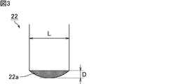
- FIG. 3 is a cross-sectional view schematically showing a method for obtaining the radius of curvature of the copper pillar bump.
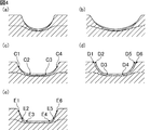
- FIG. 4A, FIG. 4B, FIG. 4C, FIG. 4D, and FIG. 4E are cross-sectional views that schematically show examples of the cross-sectional shape of the recesses.
- FIG. 4A, FIG. 4B, FIG. 4C, FIG. 4D, and FIG. 4E are cross-sectional views that schematically show examples of the cross-sectional shape of the recesses.
- FIG. 4A, FIG. 4B, FIG. 4C, FIG. 4D, and FIG. 4E are
- FIG. 5 is a cross-sectional view schematically showing a method for obtaining the radius of curvature of a recess having a bathtub-shaped cross-sectional shape.
- FIG. 6A and FIG. 6B are cross-sectional views schematically showing examples of surface electrodes provided in the recesses.
- FIG. 7A and FIG. 7B are cross-sectional views schematically illustrating another example of the electronic device of the present invention.
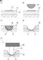
- FIG. 8A, FIG. 8B, FIG. 8C, FIG. 8D, and FIG. 8E are cross-sectional views schematically showing an example of a method for manufacturing the electronic device shown in FIG. is there.
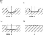
- 9 (a), 9 (b), 9 (c), and 9 (d) show electronic components on the multilayer ceramic substrates of Example 1, Example 2, Comparative Example 1, and Comparative Example 2, respectively. It is sectional drawing which showed the position to mount typically.
- the present invention is not limited to the following configurations, and can be applied with appropriate modifications without departing from the scope of the present invention.
- the present invention also includes a combination of two or more desirable configurations of the present invention described below.
- FIG. 1 is a cross-sectional view schematically showing an example of an electronic device of the present invention.
- cross section means a cross section in the thickness direction of the multilayer ceramic substrate.
- the electronic component 20 is mounted on the multilayer ceramic substrate 10.
- the electronic component 20 includes a connection terminal 21 on the mounting surface side, and the connection terminal 21 has an R shape (rounded shape) on the mounting surface side in a cross-sectional view.
- the multilayer ceramic substrate 10 includes a surface electrode 11 for connecting to the connection terminal 21.
- a recess 12 is formed at a position corresponding to the connection terminal 21, and the recess 12 has an R shape in a cross-sectional view.
- a surface electrode 11 is provided in a part of the recess 12, and the surface electrode 11 and the connection terminal 21 are electrically connected. As shown in FIG. 1, the surface electrode 11 also has an R shape in cross-sectional view.
- the electronic component constituting the electronic device of the present invention is composed of, for example, an active component, a passive component, or a composite thereof.
- active components include semiconductor elements such as transistors, diodes, ICs, and LSIs.
- passive components include chip components such as resistors, capacitors, and inductors, vibrators, filters, and the like.
- the electronic component includes a connection terminal having an R shape in cross-sectional view on the mounting surface side.
- a connection terminal having an R shape in cross-sectional view on the mounting surface side.
- the electronic component is made of a semiconductor element such as an IC
- a bump such as a copper pillar bump or a solder bump corresponds to the connection terminal.
- the electronic component is a chip component such as a capacitor
- the external electrode corresponds to the connection terminal.
- FIG. 2A is a cross-sectional view schematically showing a copper pillar bump which is an example of a connection terminal
- FIG. 2B is a cross-sectional view schematically showing a solder bump which is another example of the connection terminal. is there.
- solder 22a is provided at the tip of a copper pillar (pillar) 22b, and the tip has an R shape.
- the solder bump 23 shown in FIG. 2B has an R shape as a whole.
- the radius of curvature Rp in the cross-sectional view of the connection terminal is not particularly limited as long as the connection terminal has an R shape in the cross-sectional view.
- the connection terminal is a solder bump
- the radius when the cross-sectional shape of the solder bump is regarded as a circle is the curvature radius Rp.
- the connection terminal is a copper pillar bump
- the radius when the cross-sectional shape of the solder provided at the tip is regarded as a part of the arc is defined as a curvature radius Rp.
- FIG. 3 is a cross-sectional view schematically showing a method for obtaining the radius of curvature of the copper pillar bump.
- the radius of curvature Rp is the chord length (length indicated by L in FIG. 3) and the arrow height (D in FIG. 3).
- Rp (L 2 + 4D 2 ) / 8D
- the chord length L is not constant, such as the planar shape of the copper pillar bump is a race track shape
- the radius of curvature Rp may be obtained by setting the length of the shortest portion as the chord length L.
- the multilayer ceramic substrate constituting the electronic device of the present invention includes a ceramic body having a ceramic layer on the surface, and a surface electrode provided on one main surface of the ceramic body.
- the ceramic body constituting the multilayer ceramic substrate has a laminated structure in which a plurality of ceramic layers are laminated, and an inner layer conductor and a via conductor are provided inside the ceramic body.
- a surface electrode may be provided on the other main surface of the ceramic body.
- the ceramic layer constituting the ceramic body preferably contains a low-temperature sintered ceramic material.
- the low-temperature sintered ceramic material means a material that can be sintered at a firing temperature of 1000 ° C. or less and can be co-fired with silver, copper, or the like among ceramic materials.
- Examples of the low-temperature sintered ceramic material contained in the ceramic layer include a glass composite low-temperature sintered ceramic material obtained by mixing borosilicate glass with a ceramic material such as quartz, alumina, and forsterite, ZnO—MgO—Al 2 Crystallized glass-based low-temperature sintered ceramic materials using O 3 —SiO 2 -based crystallized glass, BaO—Al 2 O 3 —SiO 2 based ceramic materials and Al 2 O 3 —CaO—SiO 2 —MgO—B 2
- Non-glass type low-temperature sintered ceramic material using O 3 type ceramic material or the like can be used.
- the inner layer conductor and via conductor provided inside the ceramic body preferably contain at least one conductive material selected from gold, silver and copper, and more preferably contain silver or copper. Since gold, silver, and copper have low resistance, they are particularly suitable when the multilayer ceramic substrate is used for high frequency.
- the surface electrode provided on one main surface of the ceramic body is for connecting to a connection terminal of an electronic component, and preferably includes at least one conductive material selected from gold, silver and copper, More preferably, it contains silver or copper.
- the surface electrode may have a single layer structure or a multilayer structure.
- the surface electrode includes a sintered layer provided on the upper surface of the ceramic layer constituting one main surface of the ceramic body, and a plating layer provided on the upper surface of the sintered layer. It is preferable to include. Only one layer may be sufficient as a sintered layer, and two or more layers may be sufficient as it.
- the plating layer may be only one layer or two or more layers.
- the sintered layer is formed by baking a conductive paste, and the plated layer is formed by applying electrolytic plating or electroless plating after forming the sintered layer.
- the maximum thickness of a surface electrode is not specifically limited, It is preferable that they are 2 micrometers or more and 20 micrometers or less.
- the configuration of the multilayer ceramic substrate is not particularly limited, and the number of ceramic layers stacked, the arrangement of surface electrodes, inner layer conductors, and via conductors can be variously changed. Moreover, you may arrange
- Examples of the metal oxide that does not substantially sinter at the sintering temperature of the low-temperature sintered ceramic material include alumina, titania, zirconia, silica, and magnesia. Among these, alumina or silica is preferable. These metal oxides may be one kind or two or more kinds.
- the mounting surface of the multilayer ceramic substrate is formed with a concave portion having an R shape in cross-section at a position corresponding to the connection terminal.
- a surface electrode is provided on at least a part of the recess, and the surface electrode and the connection terminal are electrically connected.
- the cross-sectional shape of the concave portion is not particularly limited as long as the concave portion has an R shape in cross-sectional view, but is preferably an arc shape or a bathtub shape.
- the cross-sectional shape of a recessed part means the cross-sectional shape of the part containing a surface electrode.
- the surface electrode excluding the plating layer also has an R shape in a sectional view, and the surface electrode including the plating layer has an R shape in a sectional view.
- FIG. 4A, FIG. 4B, FIG. 4C, FIG. 4D, and FIG. 4E are cross-sectional views that schematically show examples of the cross-sectional shape of the recesses.
- a cross-sectional shape of the concave portion an arc shape as shown in FIG. 4A, an elliptic arc shape as shown in FIG. 4B, and as shown in FIG. 4C, FIG. 4D and FIG.
- the bathtub shape means an R shape having a straight base in a sectional view.
- C1 to C2 are arcuate
- C2 to C3 are linear
- C3 to C4 are arcuate.
- D1 to D3 are curved
- D3 to D4 are linear
- D4 to D6 are curved
- D2 and D5 exist as inflection points.
- E1 to E2 are linear
- E2 to E3 are arcs
- E3 to E4 are linear
- E4 to E5 are arcs
- E5 to E6 are linear.
- the radius of curvature Rs in the sectional view of the recess is not particularly limited as long as the recess has an R shape in the sectional view.
- the radius is the curvature radius Rs.
- the radius of the portion that comes into contact with the connection terminal is defined as a curvature radius Rs.
- FIG. 5 is a cross-sectional view schematically showing a method for obtaining the radius of curvature of a recess having a bathtub-shaped cross-sectional shape.
- the position A corresponding to the end of the copper pillar bump 22, the position B corresponding to the center of the copper pillar bump 22, and the center between the end and the center.
- the coordinates of the position C corresponding to the point are obtained, and the radius of the circle passing through the three points is defined as the curvature radius Rs.
- the position A is the side close to the outer periphery of the recess 12.
- the coordinates of the portion including the surface electrode 11 are obtained.
- the surface electrode 11 includes a plating layer
- the coordinates of the portion excluding the plating layer are obtained.
- connection terminal is a copper pillar bump
- the curvature radius Rs can also be obtained by the same method as described above even in the case of a connection terminal such as a solder bump.
- the value of Rp / Rs is not less than 0.1 and not more than 1.0, where Rs is the radius of curvature in the sectional view of the recess and Rp is the radius of curvature in the sectional view of the connection terminal. Is preferred.
- the value of Rp / Rs is more preferably 0.2 or more and 1.0 or less.
- the maximum depth of the concave portion excluding the plating layer is not particularly limited, but is preferably 3 ⁇ m or more and 20 ⁇ m or less.
- the structure of the surface electrode is not particularly limited as long as the surface electrode is provided on at least a part of the recess.
- the surface electrode may be provided in a part of the recess, or may be provided on the entire surface of the recess.
- the surface electrode provided in the recessed part may be electrically connected with the surface electrode provided in surfaces other than a recessed part.
- FIG. 6A and FIG. 6B are cross-sectional views schematically showing examples of surface electrodes provided in the recesses.
- the surface electrode 11 provided in a part of the recess 12 and the surface electrode 13 provided on the surface other than the recess 12 are electrically connected.
- FIG. 6B The surface electrode 11 provided on the entire surface of the recess 12 and the surface electrodes 13 and 14 provided on the surface other than the recess 12 are electrically connected.
- the mounting surface of the multilayer ceramic substrate does not need to have the recesses formed at positions corresponding to all the connection terminals.
- the recessed part should just be formed in the position corresponding to a connection terminal.
- FIG. 7A and FIG. 7B are cross-sectional views schematically illustrating another example of the electronic device of the present invention.
- the electronic component 20 is shown separated from the multilayer ceramic substrate 10 for convenience.
- the recesses 12 having the same depth are formed at positions corresponding to all the connection terminals 21.
- the length of the connection terminal 21 provided in the electronic component 20 is different, the length of the connection terminal 21 is set so that the electronic component 20 does not tilt with respect to the multilayer ceramic substrate 10. Accordingly, it is preferable that the recesses 12 having different depths are formed.
- the recessed part does not need to be formed in the position corresponding to a short connection terminal.
- FIG. 8A, FIG. 8B, FIG. 8C, FIG. 8D, and FIG. 8E are cross-sectional views schematically showing an example of a method for manufacturing the electronic device shown in FIG. is there.
- the ceramic green sheet becomes a ceramic layer after firing.
- the ceramic green sheet is obtained by forming a slurry containing a ceramic raw material powder such as a low-temperature sintered ceramic material, an organic binder, and a solvent into a sheet shape by a doctor blade method or the like.
- the slurry may contain various additives such as a dispersant and a plasticizer.
- a through hole for a via conductor is formed in a specific ceramic green sheet.
- a conductive paste body to be a via conductor is formed.
- a conductive paste layer to be an inner layer conductor is formed on a specific ceramic green sheet by a method such as screen printing.
- a conductive paste layer 11 'to be the surface electrode 11 is formed on the ceramic green sheet 15' disposed on the surface after lamination.
- the conductive paste layer 11 ′ can be formed by a method such as screen printing using a conductive paste having the same composition as the conductive paste, for example.
- a plurality of ceramic green sheets 15 ′ are stacked and pressure-bonded to produce an unfired stacked body 10 ′.
- a portion corresponding to the connection terminal of the electronic component in the unfired laminated body 10 ′ is pressed using a mold 30 having a predetermined shape.
- a concave portion 12 having an R shape in a cross-sectional view is formed on the surface of the unfired laminate 10 '.
- a conductive paste layer 11 ′ is provided in a part of the recess 12.
- a concave portion having a desired shape can be formed by changing the shape of the mold.
- the recess can be formed by drilling, laser processing, or the like.
- the electronic component 20 including the connection terminal 21 having an R shape in cross-sectional view on the mounting surface side is mounted on the multilayer ceramic substrate 10. Specifically, the connection terminal 21 of the electronic component 20 is brought into contact with the surface electrode 11 of the multilayer ceramic substrate 10 to make the surface electrode 11 and the connection terminal 21 conductive.
- a constraining green sheet containing an oxide that does not substantially sinter at the temperature at which the ceramic green sheet sinters is prepared, and laminated in a state where the constraining green sheets are arranged on both main surfaces of the unfired laminate.
- the body may be fired.
- an unfired laminated composite in which a restraining green sheet is disposed between ceramic green sheets may be fired, and furthermore, a restraining green sheet is disposed on both main surfaces of the unfired laminated composite.
- the laminated composite may be fired.
- the constraining green sheet does not sinter substantially at the time of firing, and thus does not shrink, and acts to suppress shrinkage in the main surface direction with respect to the laminated body or laminated composite.
- the dimensional accuracy of the multilayer ceramic substrate can be increased.
- the constraining green sheet is preferably formed from a slurry containing the above oxide powder, an organic binder, and a solvent into a sheet shape by a doctor blade method or the like.
- the slurry may contain various additives such as a dispersant and a plasticizer.
- alumina titania, zirconia, silica, magnesia and the like
- alumina titania, zirconia, silica, magnesia and the like
- a multilayer ceramic substrate constituting the electronic device is also one aspect of the present invention.
- the ceramic sheet 1 is a ceramic green sheet that becomes a ceramic layer of a multilayer ceramic substrate.
- powders of SiO 2 , BaCO 3 , Al 2 O 3 , ZrO 2 , CaCO 3 , B 2 O 3 , MnCO 3 , TiO 2 and Mg (OH) 2 were prepared.
- An organic binder, a dispersant and a plasticizer were added to the above starting raw material powder to prepare a ceramic slurry.
- a ceramic slurry was formed into a sheet shape on a PET film by a doctor blade method and dried to prepare a ceramic sheet 1.
- the ceramic sheet 2 is a constraining green sheet laminated inside the multilayer ceramic substrate.
- Alumina powder and B—Si—Ba-based glass powder were weighed so as to have a predetermined composition ratio, mixed and pulverized, and then a ceramic slurry was prepared by the same procedure as for ceramic sheet 1 to prepare ceramic sheet 2.
- the ceramic sheet 3 is a constraining green sheet disposed on the main surface of the multilayer ceramic substrate.
- the alumina powder and the glass powder were weighed so as to have a predetermined composition ratio, mixed and pulverized, and then a ceramic slurry was prepared by the same procedure as the ceramic sheet 1 to prepare the ceramic sheet 3.
- the conductive paste was printed on specific ceramic sheets 1, 2 and 3 by a screen printing method.
- the ceramic sheet was cut into 100 mm ⁇ 100 mm, and then pressed at a temperature of 50 ° C. or higher and 80 ° C. or lower and a pressure of 50 MPa or higher and 200 MPa or lower to obtain an unfired laminated composite.
- this laminated composite is arrange
- Step of firing the unfired laminated composite While adjusting the unfired laminated composite to an atmosphere condition in which Cu is not oxidized in an H 2 / N 2 / H 2 O atmosphere, the temperature is raised to a firing temperature of 850 ° C. to 1050 ° C. and held for 60 minutes to 90 minutes. Then, by cooling to room temperature, a multilayer ceramic substrate having a surface electrode in an arcuate recess was produced. Next, after the unsintered ceramic sheet 3 disposed on the surface of the multilayer ceramic substrate prepared after the firing is removed by ultrasonic cleaning or the like, electrolysis is performed on the surface electrode formed on the surface of the multilayer ceramic substrate. A plating layer was formed by performing plating or electroless plating.
- Example 2 Production of multilayer ceramic substrate having bathtub-shaped recesses
- the surface of the unsintered laminated composite has a bathtub shape in the cross-sectional view.
- a multilayer ceramic substrate was produced in the same manner as in Example 1 except that the recess was formed.
- Example 2 Production of multilayer ceramic substrate having no recess
- a multilayer ceramic substrate was produced in the same manner as in Example 1 except that the unsintered multilayer composite was not pressed using a mold and no recess was formed on the surface of the unsintered multilayer composite. did.
- an IC containing an internal continuity check pattern was prepared as an electronic component, and bumps serving as connection terminals were attached to the electrode portions of the IC.
- bumps solder bumps and copper pillar bumps were used.
- FIG. 9A shows electronic components on the multilayer ceramic substrates of Example 1, Example 2, Comparative Example 1, and Comparative Example 2, respectively. It is sectional drawing which showed the position to mount typically. With respect to the surface electrode of the multilayer ceramic substrate of Example 1 formed in the arc-shaped recess, as shown in FIG. 9A, the center of the recess (position indicated as 0 in FIG. 9A). The IC is mounted at a position 30 ⁇ m away from the center (position shown as 30 in FIG. 9A), 50 ⁇ m away from the center (position shown as 50 in FIG. 9A), Poor conduction was evaluated at three locations with distances from the center of 0 ⁇ m, 30 ⁇ m, and 50 ⁇ m.
- FIG. 9A shows the center of the recess
- FIG. 9B also shows the surface electrode of the multilayer ceramic substrate of Example 2 formed in the bathtub-shaped recess and the surface electrode of the multilayer ceramic substrate of Comparative Example 1 formed in the rectangular recess.
- electrical_connection defect was evaluated in three places whose distances from a center part are 0 micrometer, 30 micrometers, and 50 micrometers.
- the center portion of the surface electrode is mounted, and the conduction failure was evaluated at one place with a distance of 0 ⁇ m from the center.
- Table 1 shows the evaluation results of poor conduction.
- the case where no continuity failure occurred was marked as ⁇
- the case where a continuity failure occurred was marked as x.
- the width of the recess was 120 ⁇ m, and the maximum depth of the recess was 10 ⁇ m or more and 30 ⁇ m or less.
- the evaluation is performed with the curvature radius of the connection terminal (bump) being constant, and when the recess is formed, the ratio (Rp / Rs) of the curvature radius Rp of the connection terminal to the curvature radius Rs of the recess is constant. And evaluated.
- the radius of curvature of the recess at a position 50 ⁇ m away from the center is defined as the radius of curvature Rs.
- Example 1 in which the arc-shaped recess was formed, when the value of Rp / Rs was 0.1 or more and 1.0 or less, the occurrence of poor conduction was suppressed, and 0.2 or more and 1 It was confirmed that the occurrence of poor conduction was particularly suppressed when the ratio was 0.0 or less.
- Example 2 in which the bathtub-shaped concave portion was formed, the occurrence of poor conduction was suppressed when the value of Rp / Rs was 0.1 or more and 1.0 or less, and 0.2 or more and 1.0 or less. In the following cases, it was confirmed that the occurrence of poor conduction was particularly suppressed.
Landscapes
- Engineering & Computer Science (AREA)
- Microelectronics & Electronic Packaging (AREA)
- Manufacturing & Machinery (AREA)
- Chemical & Material Sciences (AREA)
- Ceramic Engineering (AREA)
- Inorganic Chemistry (AREA)
- Production Of Multi-Layered Print Wiring Board (AREA)
- Electric Connection Of Electric Components To Printed Circuits (AREA)
- Structures For Mounting Electric Components On Printed Circuit Boards (AREA)
- Ceramic Capacitors (AREA)
Abstract
本発明の電子デバイスは、多層セラミック基板に電子部品が実装された電子デバイスであって、上記電子部品は、断面視でR形状を有する接続端子を実装面側に備え、上記多層セラミック基板は、上記接続端子と接続するための表面電極を備え、上記多層セラミック基板の実装面には、上記接続端子に対応する位置に、断面視でR形状を有する凹部が形成されており、上記表面電極は、上記凹部の少なくとも一部に設けられており、上記接続端子と導通していることを特徴とする。
Description
本発明は、多層セラミック基板に電子部品が実装された電子デバイスに関する。また、本発明は、電子部品を実装するための多層セラミック基板に関する。
半導体チップ等の電子部品を基板上に実装する方法として、特許文献1には、突起電極と上記突起電極よりも高さが高い位置合わせ突起とが形成された電子部品を配線電極付き基板に実装する場合において、上記基板には、上記位置合わせ突起の位置に対応して斜面を有する凹部が形成され、その凹部の底部に電極が形成されるとともに、上記突起電極に対応した部分に配線電極が形成されており、上記位置合わせ突起を上記凹部に係合させて押圧して位置合わせ突起を変形させる旨の電子部品の実装方法が実質的に記載されている。上記構成によれば、狭ピッチや微細配線基板への位置ずれ実装(接続)による信頼性の低下を回避できるとされている。
特許文献1に記載されている電子部品の実装方法では、実装の完了状態における位置合わせ突起の高さを他の突起電極の高さと揃えるために基板の表面に凹部が形成されているが、位置合わせ突起に限らず、高さが異なる複数の接続端子を備える電子部品を基板に実装する場合においても、表面に凹部が形成された基板を用いることができる。
しかし、電子部品を基板に実装するために、半田バンプや銅ピラーバンプ等の接続端子を基板表面の凹部に設けられた表面電極と当接させる際、電子部品が大きなダメージを受けてしまい、導通不良が生じるおそれがある。
本発明は上記の問題を解決するためになされたものであり、多層セラミック基板に電子部品が実装された電子デバイスにおいて、実装時における電子部品のダメージを低減し、導通不良の発生を抑えることができる電子デバイスを提供することを目的とする。本発明はまた、実装時における電子部品のダメージを低減することができる多層セラミック基板を提供することを目的とする。
本発明の電子デバイスは、多層セラミック基板に電子部品が実装された電子デバイスであって、上記電子部品は、断面視でR形状を有する接続端子を実装面側に備え、上記多層セラミック基板は、上記接続端子と接続するための表面電極を備え、上記多層セラミック基板の実装面には、上記接続端子に対応する位置に、断面視でR形状を有する凹部が形成されており、上記表面電極は、上記凹部の少なくとも一部に設けられており、上記接続端子と導通していることを特徴とする。
本発明の電子デバイスでは、R形状を有する接続端子に対応する位置に、R形状を有する凹部を基板の表面に形成するとともに、その凹部の少なくとも一部に表面電極を設けている。従来のように凹部の底面が平坦である場合には、電子部品を多層セラミック基板に実装する際に接続端子と表面電極とが点で接触し、応力を大きく受けてしまう。これに対し、本発明の電子デバイスでは、電子部品を多層セラミック基板に実装する際に接続端子と表面電極とが面で接触することができる。したがって、接続端子と表面電極が点で接触する場合に比べて応力が緩和されるため、電子部品のダメージを低減し、導通不良の発生を抑えることができる。
本発明の電子デバイスにおいては、上記凹部の断面形状が円弧状又はバスタブ形状であることが好ましい。この場合、接続端子と表面電極とが面で接触しやすくなるため、電子部品のダメージをより低減することができる。
本発明の電子デバイスにおいては、上記凹部の断面視における曲率半径をRs、上記接続端子の断面視における曲率半径をRpとしたとき、Rp/Rsの値が0.1以上、1.0以下であることが好ましい。この場合、導通不良の発生をより抑えることができる。
本発明の多層セラミック基板は、電子部品を実装するための多層セラミック基板であって、上記多層セラミック基板は、上記電子部品の接続端子と接続するための表面電極を備え、上記多層セラミック基板の実装面には、上記接続端子に対応する位置に、断面視でR形状を有する凹部が形成されており、上記表面電極は、上記凹部の少なくとも一部に設けられていることを特徴とする。
本発明の多層セラミック基板では、接続端子に対応する位置に、R形状を有する凹部を基板の表面に形成するとともに、その凹部の少なくとも一部に表面電極を設けている。これにより、接続端子がR形状を有する場合に、接続端子と表面電極とが面で接触することができるため、両者が点で接触する場合に比べて応力が緩和される。そのため、電子部品のダメージを低減し、導通不良の発生を抑えることができる。
本発明の多層セラミック基板においては、上記凹部の断面形状が円弧状又はバスタブ形状であることが好ましい。この場合、接続端子と表面電極とが面で接触しやすくなるため、電子部品のダメージをより低減することができる。
本発明によれば、多層セラミック基板に電子部品が実装された電子デバイスにおいて、実装時における電子部品のダメージを低減し、導通不良の発生を抑えることができる電子デバイスを提供することができる。
以下、本発明の電子デバイスについて説明する。
しかしながら、本発明は、以下の構成に限定されるものではなく、本発明の要旨を変更しない範囲において適宜変更して適用することができる。なお、以下において記載する本発明の個々の望ましい構成を2つ以上組み合わせたものもまた本発明である。
しかしながら、本発明は、以下の構成に限定されるものではなく、本発明の要旨を変更しない範囲において適宜変更して適用することができる。なお、以下において記載する本発明の個々の望ましい構成を2つ以上組み合わせたものもまた本発明である。
図1は、本発明の電子デバイスの一例を模式的に示す断面図である。
本明細書において、単に「断面」と記載する場合には、多層セラミック基板の厚み方向の断面を意味する。
本明細書において、単に「断面」と記載する場合には、多層セラミック基板の厚み方向の断面を意味する。
図1には全体的な構成が示されていないが、電子デバイス1においては、多層セラミック基板10に電子部品20が実装されている。電子部品20は、接続端子21を実装面側に備えており、接続端子21は、断面視でR形状(rounded shape)を実装面側に有している。多層セラミック基板10は、接続端子21と接続するための表面電極11を備えている。多層セラミック基板10の実装面には、接続端子21に対応する位置に凹部12が形成されており、凹部12は、断面視でR形状を有している。凹部12の一部には表面電極11が設けられており、表面電極11と接続端子21とが導通している。なお、図1に示すように、表面電極11も、断面視でR形状を有している。
本発明の電子デバイスを構成する電子部品は、例えば、能動部品、受動部品、あるいは、それらの複合体からなっている。能動部品としては、例えば、トランジスタ、ダイオード、IC又はLSI等の半導体素子が挙げられ、受動部品としては、例えば、抵抗、コンデンサ又はインダクタ等のチップ部品や、振動子、フィルタ等が挙げられる。
本発明の電子デバイスにおいて、電子部品は、断面視でR形状を有する接続端子を実装面側に備えている。例えば、電子部品がIC等の半導体素子からなる場合、銅ピラーバンプや半田バンプ等のバンプが接続端子に相当する。また、電子部品がコンデンサ等のチップ部品からなる場合、外部電極が接続端子に相当する。
図2(a)は、接続端子の一例である銅ピラーバンプを模式的に示す断面図であり、図2(b)は、接続端子の別の一例である半田バンプを模式的に示す断面図である。
図2(a)に示す銅ピラーバンプ22では、銅製の柱(ピラー)22bの先端に半田22aが設けられており、先端がR形状を有している。また、図2(b)に示す半田バンプ23では、全体がR形状を有している。
図2(a)に示す銅ピラーバンプ22では、銅製の柱(ピラー)22bの先端に半田22aが設けられており、先端がR形状を有している。また、図2(b)に示す半田バンプ23では、全体がR形状を有している。
本発明の電子デバイスにおいては、接続端子が断面視でR形状を有する限り、接続端子の断面視における曲率半径Rpは特に限定されない。
例えば、接続端子が半田バンプである場合、半田バンプの断面形状を円とみなしたときの半径を曲率半径Rpとする。また、接続端子が銅ピラーバンプである場合、先端に設けられた半田の断面形状を円弧の一部とみなしたときの半径を曲率半径Rpとする。
例えば、接続端子が半田バンプである場合、半田バンプの断面形状を円とみなしたときの半径を曲率半径Rpとする。また、接続端子が銅ピラーバンプである場合、先端に設けられた半田の断面形状を円弧の一部とみなしたときの半径を曲率半径Rpとする。
図3は、銅ピラーバンプの曲率半径を求める方法を模式的に示す断面図である。
銅ピラーバンプ22の先端に設けられた半田22aの断面形状を円弧の一部とみなす場合、曲率半径Rpは、弦長(図3中、Lで示す長さ)及び矢高(図3中、Dで示す長さ)を測定することにより、以下の式
Rp=(L2+4D2)/8D
から求めることができる。
なお、銅ピラーバンプの平面形状がレーストラック形状である等、弦長Lが一定でない場合、最も短い箇所の長さを弦長Lとして曲率半径Rpを求めればよい。
銅ピラーバンプ22の先端に設けられた半田22aの断面形状を円弧の一部とみなす場合、曲率半径Rpは、弦長(図3中、Lで示す長さ)及び矢高(図3中、Dで示す長さ)を測定することにより、以下の式
Rp=(L2+4D2)/8D
から求めることができる。
なお、銅ピラーバンプの平面形状がレーストラック形状である等、弦長Lが一定でない場合、最も短い箇所の長さを弦長Lとして曲率半径Rpを求めればよい。
本発明の電子デバイスを構成する多層セラミック基板は、表面にセラミック層を有するセラミック素体と、セラミック素体の一方主面に設けられた表面電極とを備えている。
多層セラミック基板を構成するセラミック素体は、複数のセラミック層が積層された積層構造を有しており、セラミック素体の内部には、内層導体及びビア導体が設けられている。また、セラミック素体の他方主面にも表面電極が設けられていてもよい。
セラミック素体を構成するセラミック層は、低温焼結セラミック材料を含有することが好ましい。低温焼結セラミック材料とは、セラミック材料のうち、1000℃以下の焼成温度で焼結可能であり、銀や銅等との同時焼成が可能である材料を意味する。
セラミック層に含有される低温焼結セラミック材料としては、例えば、クオーツやアルミナ、フォルステライト等のセラミック材料にホウ珪酸ガラスを混合してなるガラス複合系低温焼結セラミック材料、ZnO-MgO-Al2O3-SiO2系の結晶化ガラスを用いた結晶化ガラス系低温焼結セラミック材料、BaO-Al2O3-SiO2系セラミック材料やAl2O3-CaO-SiO2-MgO-B2O3系セラミック材料等を用いた非ガラス系低温焼結セラミック材料等が挙げられる。
セラミック素体の内部に設けられる内層導体及びビア導体は、金、銀及び銅から選択される少なくとも1種の導電材料を含むことが好ましく、銀又は銅を含むことがより好ましい。金、銀及び銅は、低抵抗であるため、特に、多層セラミック基板が高周波用途である場合に適している。
セラミック素体の一方主面に設けられた表面電極は、電子部品の接続端子と接続するためのものであり、金、銀及び銅から選択される少なくとも1種の導電材料を含むことが好ましく、銀又は銅を含むことがより好ましい。
表面電極は、1層構造を有していてもよいし、複層構造を有していてもよい。表面電極が複層構造を有する場合、表面電極は、セラミック素体の一方主面を構成するセラミック層の上面に設けられた焼結層と、焼結層の上面に設けられためっき層とを含むことが好ましい。焼結層は、1層のみでもよいし、2層以上でもよい。めっき層も、1層のみでもよいし、2層以上でもよい。
なお、焼結層は、導電ペーストを焼き付けることによって形成されたものであり、めっき層は、焼結層を形成した後に電解めっき又は無電解めっきを施すことによって形成されたものである。
なお、焼結層は、導電ペーストを焼き付けることによって形成されたものであり、めっき層は、焼結層を形成した後に電解めっき又は無電解めっきを施すことによって形成されたものである。
表面電極の最大厚みは特に限定されないが、2μm以上、20μm以下であることが好ましい。
本発明の電子デバイスにおいて、多層セラミック基板の構成は特に限定されず、セラミック層の積層数や、表面電極、内層導体及びビア導体の配置等については種々に変更することができる。
また、低温焼結セラミック材料を含有するセラミック層の間に、上記低温焼結セラミック材料の焼結温度では実質的に焼結しない金属酸化物を含有する拘束層を配置してもよい。
また、低温焼結セラミック材料を含有するセラミック層の間に、上記低温焼結セラミック材料の焼結温度では実質的に焼結しない金属酸化物を含有する拘束層を配置してもよい。
低温焼結セラミック材料の焼結温度では実質的に焼結しない金属酸化物としては、例えば、アルミナ、チタニア、ジルコニア、シリカ、マグネシア等が挙げられ、これらの中ではアルミナ又はシリカが好ましい。これらの金属酸化物は、1種でもよく、2種以上でもよい。
本発明の電子デバイスにおいて、多層セラミック基板の実装面には、接続端子に対応する位置に、断面視でR形状を有する凹部が形成されている。凹部の少なくとも一部には表面電極が設けられており、表面電極と接続端子とが導通している。
本発明の電子デバイスにおいては、凹部が断面視でR形状を有する限り、凹部の断面形状は特に限定されないが、円弧状又はバスタブ形状であることが好ましい。
なお、凹部の断面形状とは、表面電極を含む部分の断面形状を意味する。ただし、表面電極がめっき層を含む場合には、めっき層を除いた部分の断面形状を意味する。したがって、本発明の電子デバイスにおいては、めっき層を除いた表面電極も、断面視でR形状を有しており、めっき層を含む表面電極が断面視でR形状を有することが好ましい。
なお、凹部の断面形状とは、表面電極を含む部分の断面形状を意味する。ただし、表面電極がめっき層を含む場合には、めっき層を除いた部分の断面形状を意味する。したがって、本発明の電子デバイスにおいては、めっき層を除いた表面電極も、断面視でR形状を有しており、めっき層を含む表面電極が断面視でR形状を有することが好ましい。
図4(a)、図4(b)、図4(c)、図4(d)及び図4(e)は、凹部の断面形状の例を模式的に示す断面図である。
凹部の断面形状としては、図4(a)に示すような円弧状、図4(b)に示すような楕円弧状、図4(c)、図4(d)及び図4(e)に示すようなバスタブ形状等が挙げられる。なお、バスタブ形状とは、断面視で、直線状の底辺を有するR形状を意味する。図4(c)では、C1からC2までが円弧状、C2からC3までが直線状、C3からC4までが円弧状になっている。図4(d)では、D1からD3までが曲線状、D3からD4までが直線状、D4からD6までが曲線状となっており、D2及びD5が変曲点として存在する。図4(e)では、E1からE2までが直線状、E2からE3までが円弧状、E3からE4までが直線状、E4からE5までが円弧状、E5からE6までが直線状となっている。
凹部の断面形状としては、図4(a)に示すような円弧状、図4(b)に示すような楕円弧状、図4(c)、図4(d)及び図4(e)に示すようなバスタブ形状等が挙げられる。なお、バスタブ形状とは、断面視で、直線状の底辺を有するR形状を意味する。図4(c)では、C1からC2までが円弧状、C2からC3までが直線状、C3からC4までが円弧状になっている。図4(d)では、D1からD3までが曲線状、D3からD4までが直線状、D4からD6までが曲線状となっており、D2及びD5が変曲点として存在する。図4(e)では、E1からE2までが直線状、E2からE3までが円弧状、E3からE4までが直線状、E4からE5までが円弧状、E5からE6までが直線状となっている。
本発明の電子デバイスにおいては、凹部が断面視でR形状を有する限り、凹部の断面視における曲率半径Rsは特に限定されない。
例えば、凹部の断面形状が円弧状である場合、その半径を曲率半径Rsとする。また、凹部の断面形状が楕円弧状又はバスタブ形状である場合、接続端子と当接する箇所の半径を曲率半径Rsとする。
例えば、凹部の断面形状が円弧状である場合、その半径を曲率半径Rsとする。また、凹部の断面形状が楕円弧状又はバスタブ形状である場合、接続端子と当接する箇所の半径を曲率半径Rsとする。
図5は、バスタブ形状の断面形状を有する凹部の曲率半径を求める方法を模式的に示す断面図である。
図5に示すように、多層セラミック基板10の凹部12において、銅ピラーバンプ22の端部に対応する位置A、銅ピラーバンプ22の中央部に対応する位置B、及び、端部と中央部との中点に対応する位置Cの座標を求め、その3点を通る円の半径を曲率半径Rsとする。位置Aは、凹部12の外周に近い側とする。なお、位置A、位置B及び位置Cの座標を求める際には、図5に示すように、表面電極11を含む部分の座標を求める。ただし、表面電極11がめっき層を含む場合には、めっき層を除いた部分の座標を求める。
図5に示すように、多層セラミック基板10の凹部12において、銅ピラーバンプ22の端部に対応する位置A、銅ピラーバンプ22の中央部に対応する位置B、及び、端部と中央部との中点に対応する位置Cの座標を求め、その3点を通る円の半径を曲率半径Rsとする。位置Aは、凹部12の外周に近い側とする。なお、位置A、位置B及び位置Cの座標を求める際には、図5に示すように、表面電極11を含む部分の座標を求める。ただし、表面電極11がめっき層を含む場合には、めっき層を除いた部分の座標を求める。
図5では、接続端子が銅ピラーバンプである場合について説明したが、半田バンプ等の接続端子の場合も、上記の同様の方法によって曲率半径Rsを求めることができる。
本発明の電子デバイスにおいては、凹部の断面視における曲率半径をRs、接続端子の断面視における曲率半径をRpとしたとき、Rp/Rsの値が0.1以上、1.0以下であることが好ましい。Rp/Rsの値は、0.2以上、1.0以下であることがより好ましい。
本発明の電子デバイスにおいて、めっき層を除いた凹部の最大深さは特に限定されないが、3μm以上、20μm以下であることが好ましい。
本発明の電子デバイスにおいては、凹部の少なくとも一部に表面電極が設けられている限り、表面電極の構造は特に限定されない。表面電極は、凹部の一部に設けられていてもよいし、凹部の全面に設けられていてもよい。また、凹部に設けられた表面電極は、凹部以外の表面に設けられた表面電極と電気的に接続されていてもよい。
図6(a)及び図6(b)は、凹部に設けられた表面電極の例を模式的に示す断面図である。
図6(a)では、凹部12の一部に設けられた表面電極11と、凹部12以外の表面に設けられた表面電極13とが電気的に接続されており、図6(b)では、凹部12の全面に設けられた表面電極11と、凹部12以外の表面に設けられた表面電極13及び14とが電気的に接続されている。
図6(a)では、凹部12の一部に設けられた表面電極11と、凹部12以外の表面に設けられた表面電極13とが電気的に接続されており、図6(b)では、凹部12の全面に設けられた表面電極11と、凹部12以外の表面に設けられた表面電極13及び14とが電気的に接続されている。
本発明の電子デバイスにおいて、電子部品が複数の接続端子を備える場合、多層セラミック基板の実装面には、全ての接続端子に対応する位置に上記凹部が形成されている必要はなく、少なくとも1つの接続端子に対応する位置に上記凹部が形成されていればよい。
図7(a)及び図7(b)は、本発明の電子デバイスの別の例を模式的に示す断面図である。図7(a)及び図7(b)では、便宜上、電子部品20を多層セラミック基板10から離して記載している。
図7(a)に示すように、電子部品20が備える接続端子21の長さが同じ場合、全ての接続端子21に対応する位置に、深さの同じ凹部12が形成されていることが好ましい。また、図7(b)に示すように、電子部品20が備える接続端子21の長さが異なる場合、多層セラミック基板10に対して電子部品20が傾かないように、接続端子21の長さに応じて深さの異なる凹部12が形成されていることが好ましい。ただし、図7(b)においては、長さの短い接続端子に対応する位置に凹部が形成されていなくてもよい。
図7(a)に示すように、電子部品20が備える接続端子21の長さが同じ場合、全ての接続端子21に対応する位置に、深さの同じ凹部12が形成されていることが好ましい。また、図7(b)に示すように、電子部品20が備える接続端子21の長さが異なる場合、多層セラミック基板10に対して電子部品20が傾かないように、接続端子21の長さに応じて深さの異なる凹部12が形成されていることが好ましい。ただし、図7(b)においては、長さの短い接続端子に対応する位置に凹部が形成されていなくてもよい。
本発明の電子デバイスは、好ましくは以下のように製造される。
図8(a)、図8(b)、図8(c)、図8(d)及び図8(e)は、図1に示す電子デバイスの製造方法の一例を模式的に示す断面図である。
図8(a)、図8(b)、図8(c)、図8(d)及び図8(e)は、図1に示す電子デバイスの製造方法の一例を模式的に示す断面図である。
まず、複数のセラミックグリーンシートを準備する。セラミックグリーンシートは、焼成後にセラミック層となるものである。
セラミックグリーンシートは、例えば低温焼結セラミック材料のようなセラミック原料の粉末と、有機バインダと溶剤とを含有するスラリーを、ドクターブレード法等によってシート状に成形したものである。上記スラリーには、分散剤、可塑剤等の種々の添加剤が含有されていてもよい。
特定のセラミックグリーンシートに、ビア導体のための貫通孔を形成する。該貫通孔に、例えば銀又は銅を含有する導電ペーストを充填することにより、ビア導体となるべき導電ペースト体を形成する。
上記導電ペーストと同じ組成の導電ペーストを用いて、例えばスクリーン印刷等の方法によって、特定のセラミックグリーンシートに、内層導体となるべき導電ペースト層を形成する。
次に、図8(a)に示すように、積層後に表面に配置されるセラミックグリーンシート15’上に、表面電極11となるべき導電ペースト層11’を形成する。導電ペースト層11’は、例えば上記導電ペーストと同じ組成の導電ペーストを用いて、スクリーン印刷等の方法によって形成することができる。続いて、複数のセラミックグリーンシート15’を積層し、圧着することにより、未焼成の積層体10’を作製する。
続いて、図8(b)に示すように、所定の形状の金型30を用いて、未焼成の積層体10’のうち、電子部品の接続端子に対応する部分をプレスする。これによって、図8(c)に示すように、未焼成の積層体10’の表面に、断面視でR形状を有する凹部12が形成される。図8(c)では、凹部12の一部に導電ペースト層11’が設けられている。
未焼成の積層体をプレスする際、金型の形状を変更することにより、所望の形状の凹部を形成することができる。また、ドリル加工、レーザー加工等によっても凹部を形成することができる。
金型を外した後、未焼成の積層体10’を焼成する。これによって、図8(d)に示すように、凹部12の表面に表面電極11を備える焼結体(多層セラミック基板10)が得られる。
なお、焼成後の焼結体に対して、電解めっき又は無電解めっきを施すことによって、表面電極の上面にめっき層を形成してもよい。
その後、図8(e)に示すように、断面視でR形状を有する接続端子21を実装面側に備える電子部品20を多層セラミック基板10に実装する。具体的には、電子部品20の接続端子21を多層セラミック基板10の表面電極11と当接させ、表面電極11と接続端子21とを導通させる。
以上により、図1に示す電子デバイス1が得られる。
なお、セラミックグリーンシートが焼結する温度では実質的に焼結しない酸化物を含有する拘束用グリーンシートを準備し、未焼成の積層体の両主面に拘束用グリーンシートを配置した状態で積層体を焼成してもよい。また、セラミックグリーンシートの間に拘束用グリーンシートを配置した未焼成の積層複合体を焼成してもよいし、さらに、未焼成の積層複合体の両主面に拘束用グリーンシートを配置した状態で積層複合体を焼成してもよい。
この場合、拘束用グリーンシートは、焼成時において実質的に焼結しないので収縮が生じず、積層体又は積層複合体に対して主面方向での収縮を抑制するように作用する。その結果、多層セラミック基板の寸法精度を高めることができる。
この場合、拘束用グリーンシートは、焼成時において実質的に焼結しないので収縮が生じず、積層体又は積層複合体に対して主面方向での収縮を抑制するように作用する。その結果、多層セラミック基板の寸法精度を高めることができる。
拘束用グリーンシートは、好ましくは、上記酸化物の粉末と有機バインダと溶剤とを含有するスラリーを、ドクターブレード法等によってシート状に成形したものである。上記スラリーには、分散剤、可塑剤等の種々の添加剤が含有されていてもよい。
上記スラリーに含有される酸化物としては、例えば、アルミナ、チタニア、ジルコニア、シリカ、マグネシア等を用いることができる。これらの中では、アルミナを用いることが好ましい。
以上、本発明の電子デバイスについて説明してきたが、上記電子デバイスを構成する多層セラミック基板もまた、本発明の1つである。
以下、本発明の電子デバイスをより具体的に開示した実施例を示す。なお、本発明は、これらの実施例のみに限定されるものではない。
[実施例1:円弧状の凹部が形成された多層セラミック基板の作製]
(セラミックシート1を準備する工程)
セラミックシート1は、多層セラミック基板のセラミック層となるセラミックグリーンシートである。
出発原料として、SiO2、BaCO3、Al2O3、ZrO2、CaCO3、B2O3、MnCO3、TiO2及びMg(OH)2の各粉末を準備した。
上述の出発原料粉末に、有機バインダ、分散剤及び可塑剤を加えて、セラミックスラリーを作製した。
次に、ドクターブレード法によってセラミックスラリーをPETフィルム上にシート状に成形し、乾燥させることにより、セラミックシート1を作製した。
(セラミックシート1を準備する工程)
セラミックシート1は、多層セラミック基板のセラミック層となるセラミックグリーンシートである。
出発原料として、SiO2、BaCO3、Al2O3、ZrO2、CaCO3、B2O3、MnCO3、TiO2及びMg(OH)2の各粉末を準備した。
上述の出発原料粉末に、有機バインダ、分散剤及び可塑剤を加えて、セラミックスラリーを作製した。
次に、ドクターブレード法によってセラミックスラリーをPETフィルム上にシート状に成形し、乾燥させることにより、セラミックシート1を作製した。
(セラミックシート2を準備する工程)
セラミックシート2は、多層セラミック基板の内部に積層される拘束用グリーンシートである。
アルミナ粉末とB-Si-Ba系ガラス粉末とを所定の組成比となるように秤量し、混合粉砕した後、セラミックシート1と同様の手順によりセラミックスラリーを作製し、セラミックシート2を作製した。
セラミックシート2は、多層セラミック基板の内部に積層される拘束用グリーンシートである。
アルミナ粉末とB-Si-Ba系ガラス粉末とを所定の組成比となるように秤量し、混合粉砕した後、セラミックシート1と同様の手順によりセラミックスラリーを作製し、セラミックシート2を作製した。
(セラミックシート3を準備する工程)
セラミックシート3は、多層セラミック基板の主面に配置される拘束用グリーンシートである。
アルミナ粉末とガラス粉末とを所定の組成比となるように秤量し、混合粉砕した後、セラミックシート1と同様の手順によりセラミックスラリーを作製し、セラミックシート3を作製した。
セラミックシート3は、多層セラミック基板の主面に配置される拘束用グリーンシートである。
アルミナ粉末とガラス粉末とを所定の組成比となるように秤量し、混合粉砕した後、セラミックシート1と同様の手順によりセラミックスラリーを作製し、セラミックシート3を作製した。
(導電ペーストを準備する工程)
Cu粉末、エチルセルロース及びテルペン系溶剤を混合し、3本ロールミルで混合分散することにより、電極形成用の導電ペーストを作製した。
Cu粉末、エチルセルロース及びテルペン系溶剤を混合し、3本ロールミルで混合分散することにより、電極形成用の導電ペーストを作製した。
(導電ペーストをセラミックシートに印刷する工程)
特定のセラミックシート1、2及び3上に、スクリーン印刷法により上記導電ペーストを印刷した。
特定のセラミックシート1、2及び3上に、スクリーン印刷法により上記導電ペーストを印刷した。
(セラミックシートを積層圧着する工程)
上記のセラミックシートを100mm×100mmにカットした後、温度50℃以上80℃以下、圧力50MPa以上200MPa以下で圧着することにより、未焼成の積層複合体を得た。なお、この積層複合体は、表面から、セラミックシート3、セラミックシート1及びセラミックシート2の順で配置されている。
上記のセラミックシートを100mm×100mmにカットした後、温度50℃以上80℃以下、圧力50MPa以上200MPa以下で圧着することにより、未焼成の積層複合体を得た。なお、この積層複合体は、表面から、セラミックシート3、セラミックシート1及びセラミックシート2の順で配置されている。
(凹部を形成する工程)
断面視で円弧状の金型を用いて、未焼成の積層複合体のうち、電子部品の接続端子に対応する部分をプレスした。これにより、未焼成の積層複合体の表面に、断面視で円弧状の凹部を形成した。なお、凹部は、焼成後の表面電極が凹部の一部に設けられるように形成した。なお、セラミックシート2及びセラミックシート1の順で積層してから、上記金型を用いてプレスすることにより、断面視で円弧状の凹部を形成した後、セラミックシート3を積層して圧着してもよい。
断面視で円弧状の金型を用いて、未焼成の積層複合体のうち、電子部品の接続端子に対応する部分をプレスした。これにより、未焼成の積層複合体の表面に、断面視で円弧状の凹部を形成した。なお、凹部は、焼成後の表面電極が凹部の一部に設けられるように形成した。なお、セラミックシート2及びセラミックシート1の順で積層してから、上記金型を用いてプレスすることにより、断面視で円弧状の凹部を形成した後、セラミックシート3を積層して圧着してもよい。
(未焼成の積層複合体を焼成する工程)
未焼成の積層複合体を、H2/N2/H2O雰囲気でCuが酸化しない雰囲気条件に調整しながら、焼成温度850℃以上1050℃以下まで昇温し、60分間以上90分間以下保持した後、室温まで冷却することにより、円弧状の凹部に表面電極を備える多層セラミック基板を作製した。次いで、上記焼成後に作製された多層セラミック基板の表面に配置された未焼結のセラミックシート3を超音波洗浄等で除去した後、上記多層セラミック基板の表面に形成された表面電極上に、電解めっき又は無電解めっきを施すことによって、めっき層を形成した。
未焼成の積層複合体を、H2/N2/H2O雰囲気でCuが酸化しない雰囲気条件に調整しながら、焼成温度850℃以上1050℃以下まで昇温し、60分間以上90分間以下保持した後、室温まで冷却することにより、円弧状の凹部に表面電極を備える多層セラミック基板を作製した。次いで、上記焼成後に作製された多層セラミック基板の表面に配置された未焼結のセラミックシート3を超音波洗浄等で除去した後、上記多層セラミック基板の表面に形成された表面電極上に、電解めっき又は無電解めっきを施すことによって、めっき層を形成した。
[実施例2:バスタブ形状の凹部が形成された多層セラミック基板の作製]
断面視で円弧状の金型に代えて、断面視でバスタブ形状の金型を用いて未焼成の積層複合体をプレスすることにより、未焼成の積層複合体の表面に、断面視でバスタブ形状の凹部を形成したことを除いて、実施例1と同様の方法で多層セラミック基板を作製した。
断面視で円弧状の金型に代えて、断面視でバスタブ形状の金型を用いて未焼成の積層複合体をプレスすることにより、未焼成の積層複合体の表面に、断面視でバスタブ形状の凹部を形成したことを除いて、実施例1と同様の方法で多層セラミック基板を作製した。
[比較例1:矩形状の凹部が形成された多層セラミック基板の作製]
断面視で円弧状の金型に代えて、断面視で矩形状の金型を用いて未焼成の積層複合体をプレスすることにより、未焼成の積層複合体の表面に、断面視で矩形状の凹部を形成したことを除いて、実施例1と同様の方法で多層セラミック基板を作製した。
断面視で円弧状の金型に代えて、断面視で矩形状の金型を用いて未焼成の積層複合体をプレスすることにより、未焼成の積層複合体の表面に、断面視で矩形状の凹部を形成したことを除いて、実施例1と同様の方法で多層セラミック基板を作製した。
[比較例2:凹部が形成されていない多層セラミック基板の作製]
金型を用いた未焼成の積層複合体のプレスを行わず、未焼成の積層複合体の表面に凹部を形成しなかったことを除いて、実施例1と同様の方法で多層セラミック基板を作製した。
金型を用いた未焼成の積層複合体のプレスを行わず、未焼成の積層複合体の表面に凹部を形成しなかったことを除いて、実施例1と同様の方法で多層セラミック基板を作製した。
[電子デバイスの評価]
実施例1、実施例2、比較例1及び比較例2の多層セラミック基板に電子部品を実装することによって電子デバイスを作製した。実装時における電子部品のダメージを評価するために、導通不良を評価した。
実施例1、実施例2、比較例1及び比較例2の多層セラミック基板に電子部品を実装することによって電子デバイスを作製した。実装時における電子部品のダメージを評価するために、導通不良を評価した。
まず、電子部品として、内部導通チェックパターンを内蔵したICを準備し、ICの電極部に接続端子であるバンプを付けた。バンプとしては、半田バンプ及び銅ピラーバンプを用いた。
図9(a)、図9(b)、図9(c)及び図9(d)は、それぞれ、実施例1、実施例2、比較例1及び比較例2の多層セラミック基板に電子部品を実装する位置を模式的に示した断面図である。
円弧状の凹部に形成された実施例1の多層セラミック基板の表面電極に対して、図9(a)に示すように、凹部の中心部(図9(a)中、0と示した位置)、中心部から30μm離れた位置(図9(a)中、30と示した位置)、中心部から50μm離れた位置(図9(a)中、50と示した位置)にICを搭載し、中心部からの距離が0μm、30μm及び50μmの3箇所で導通不良を評価した。
バスタブ形状の凹部に形成された実施例2の多層セラミック基板の表面電極、及び、矩形状の凹部に形成された比較例1の多層セラミック基板の表面電極に対しても、それぞれ図9(b)及び図9(c)に示すように、中心部からの距離が0μm、30μm及び50μmの3箇所で導通不良を評価した。
凹部が形成されていない比較例2の多層セラミック基板の表面電極に対しては、図9(d)に示すように、表面電極の中心部(図9(d)中、0と示した位置)にICを搭載し、中心部からの距離が0μmの1箇所で導通不良を評価した。
円弧状の凹部に形成された実施例1の多層セラミック基板の表面電極に対して、図9(a)に示すように、凹部の中心部(図9(a)中、0と示した位置)、中心部から30μm離れた位置(図9(a)中、30と示した位置)、中心部から50μm離れた位置(図9(a)中、50と示した位置)にICを搭載し、中心部からの距離が0μm、30μm及び50μmの3箇所で導通不良を評価した。
バスタブ形状の凹部に形成された実施例2の多層セラミック基板の表面電極、及び、矩形状の凹部に形成された比較例1の多層セラミック基板の表面電極に対しても、それぞれ図9(b)及び図9(c)に示すように、中心部からの距離が0μm、30μm及び50μmの3箇所で導通不良を評価した。
凹部が形成されていない比較例2の多層セラミック基板の表面電極に対しては、図9(d)に示すように、表面電極の中心部(図9(d)中、0と示した位置)にICを搭載し、中心部からの距離が0μmの1箇所で導通不良を評価した。
導通不良の評価結果を表1に示す。表1では、導通不良が発生しなかった場合を○、導通不良が発生した場合を×とした。
なお、凹部の幅は120μm、凹部の最大深さは10μm以上30μm以下とした。また、接続端子(バンプ)の曲率半径を一定にして評価するとともに、凹部が形成されている場合には、凹部の曲率半径Rsに対する接続端子の曲率半径Rpの比(Rp/Rs)を一定にして評価した。バスタブ形状の凹部については、中心部から50μm離れた位置における凹部の曲率半径を上記曲率半径Rsとした。
なお、凹部の幅は120μm、凹部の最大深さは10μm以上30μm以下とした。また、接続端子(バンプ)の曲率半径を一定にして評価するとともに、凹部が形成されている場合には、凹部の曲率半径Rsに対する接続端子の曲率半径Rpの比(Rp/Rs)を一定にして評価した。バスタブ形状の凹部については、中心部から50μm離れた位置における凹部の曲率半径を上記曲率半径Rsとした。

表1より、矩形状の凹部が形成された比較例1、及び、凹部が形成されていない比較例2では、接続端子と表面電極とが点で接触するため、導通不良が発生したと考えられる。一方、円弧状の凹部が形成された実施例1では、接続端子と表面電極とが面で接触するため、導通不良が発生しなかったと考えられる。また、バスタブ形状の凹部が形成された実施例2では、中心部から50μm離れた位置では接続端子と表面電極とが面で接触するため、導通不良が発生しなかったと考えられる。
以下、実施例1及び実施例2の多層セラミック基板に対して、中心部から50μm離れた位置において、Rp/Rsの値を表2に示す範囲に変更した場合の導通不良を評価した。導通不良の評価結果を表2に示す。表2では、1000個のICに対して、導通不良の発生数が0個の場合を◎(優)、1個以上10個以下の場合を○(良)、11個以上50個以下の場合を△(可)、51個以上の場合を×(不良)とした。

表2より、円弧状の凹部が形成された実施例1では、Rp/Rsの値が0.1以上、1.0以下である場合に導通不良の発生が抑えられ、0.2以上、1.0以下である場合に導通不良の発生が特に抑えられることが確認された。
また、バスタブ形状の凹部が形成された実施例2では、Rp/Rsの値が0.1以上、1.0以下である場合に導通不良の発生が抑えられ、0.2以上、1.0以下である場合に導通不良の発生が特に抑えられることが確認された。
1 電子デバイス
10 多層セラミック基板
11,13,14 表面電極
12 凹部
20 電子部品
21 接続端子
22 銅ピラーバンプ(接続端子)
23 半田バンプ(接続端子)
10 多層セラミック基板
11,13,14 表面電極
12 凹部
20 電子部品
21 接続端子
22 銅ピラーバンプ(接続端子)
23 半田バンプ(接続端子)
Claims (5)
- 多層セラミック基板に電子部品が実装された電子デバイスであって、
前記電子部品は、断面視でR形状を有する接続端子を実装面側に備え、
前記多層セラミック基板は、前記接続端子と接続するための表面電極を備え、
前記多層セラミック基板の実装面には、前記接続端子に対応する位置に、断面視でR形状を有する凹部が形成されており、
前記表面電極は、前記凹部の少なくとも一部に設けられており、前記接続端子と導通していることを特徴とする電子デバイス。 - 前記凹部の断面形状が円弧状又はバスタブ形状である請求項1に記載の電子デバイス。
- 前記凹部の断面視における曲率半径をRs、前記接続端子の断面視における曲率半径をRpとしたとき、Rp/Rsの値が0.1以上、1.0以下である請求項1又は2に記載の電子デバイス。
- 電子部品を実装するための多層セラミック基板であって、
前記多層セラミック基板は、前記電子部品の接続端子と接続するための表面電極を備え、
前記多層セラミック基板の実装面には、前記接続端子に対応する位置に、断面視でR形状を有する凹部が形成されており、
前記表面電極は、前記凹部の少なくとも一部に設けられていることを特徴とする多層セラミック基板。 - 前記凹部の断面形状が円弧状又はバスタブ形状である請求項4に記載の多層セラミック基板。
Priority Applications (3)
| Application Number | Priority Date | Filing Date | Title |
|---|---|---|---|
| JP2018536977A JPWO2018042846A1 (ja) | 2016-08-30 | 2017-06-27 | 電子デバイス及び多層セラミック基板 |
| CN201780052927.1A CN109644559A (zh) | 2016-08-30 | 2017-06-27 | 电子器件以及多层陶瓷基板 |
| US16/283,858 US20190191565A1 (en) | 2016-08-30 | 2019-02-25 | Electronic device and multilayer ceramic substrate |
Applications Claiming Priority (2)
| Application Number | Priority Date | Filing Date | Title |
|---|---|---|---|
| JP2016168314 | 2016-08-30 | ||
| JP2016-168314 | 2016-08-30 |
Related Child Applications (1)
| Application Number | Title | Priority Date | Filing Date |
|---|---|---|---|
| US16/283,858 Continuation US20190191565A1 (en) | 2016-08-30 | 2019-02-25 | Electronic device and multilayer ceramic substrate |
Publications (1)
| Publication Number | Publication Date |
|---|---|
| WO2018042846A1 true WO2018042846A1 (ja) | 2018-03-08 |
Family
ID=61301541
Family Applications (1)
| Application Number | Title | Priority Date | Filing Date |
|---|---|---|---|
| PCT/JP2017/023542 Ceased WO2018042846A1 (ja) | 2016-08-30 | 2017-06-27 | 電子デバイス及び多層セラミック基板 |
Country Status (4)
| Country | Link |
|---|---|
| US (1) | US20190191565A1 (ja) |
| JP (1) | JPWO2018042846A1 (ja) |
| CN (1) | CN109644559A (ja) |
| WO (1) | WO2018042846A1 (ja) |
Cited By (2)
| Publication number | Priority date | Publication date | Assignee | Title |
|---|---|---|---|---|
| JP2020191436A (ja) * | 2019-05-22 | 2020-11-26 | レノボ・シンガポール・プライベート・リミテッド | 基板、電子基板および電子基板の製造方法 |
| JP2021022699A (ja) * | 2019-07-30 | 2021-02-18 | 京セラ株式会社 | 配線基体および電子装置 |
Families Citing this family (3)
| Publication number | Priority date | Publication date | Assignee | Title |
|---|---|---|---|---|
| JP7607438B2 (ja) * | 2020-11-13 | 2024-12-27 | ローム株式会社 | 半導体装置 |
| CN114665902A (zh) * | 2020-12-22 | 2022-06-24 | 华为技术有限公司 | 基于低温共烧陶瓷的射频器件及电子设备 |
| JP2023156659A (ja) * | 2022-04-13 | 2023-10-25 | 富士電機株式会社 | 半導体装置 |
Citations (3)
| Publication number | Priority date | Publication date | Assignee | Title |
|---|---|---|---|---|
| JPH0241476U (ja) * | 1988-09-14 | 1990-03-22 | ||
| JPH11121527A (ja) * | 1997-10-21 | 1999-04-30 | Pfu Ltd | ベアチップ実装方法およびセラミック基板の製造方法およびセラミック基板ならびに半導体装置 |
| JP2008021751A (ja) * | 2006-07-11 | 2008-01-31 | National Institute Of Advanced Industrial & Technology | 電極、半導体チップ、基板、半導体チップの電極接続構造、半導体モジュールおよびその製造方法 |
Family Cites Families (11)
| Publication number | Priority date | Publication date | Assignee | Title |
|---|---|---|---|---|
| JPS62229896A (ja) * | 1986-03-29 | 1987-10-08 | 株式会社東芝 | 印刷配線基板 |
| AU645283B2 (en) * | 1990-01-23 | 1994-01-13 | Sumitomo Electric Industries, Ltd. | Substrate for packaging a semiconductor device |
| US5290970A (en) * | 1992-09-18 | 1994-03-01 | Unisys Corporation | Multilayer printed circuit board rework method and rework pin |
| US5543586A (en) * | 1994-03-11 | 1996-08-06 | The Panda Project | Apparatus having inner layers supporting surface-mount components |
| JPH08279670A (ja) * | 1995-04-07 | 1996-10-22 | Hitachi Ltd | 電子部品の表面実装構造 |
| US5928767A (en) * | 1995-06-07 | 1999-07-27 | Dexter Corporation | Conductive film composite |
| JP3395621B2 (ja) * | 1997-02-03 | 2003-04-14 | イビデン株式会社 | プリント配線板及びその製造方法 |
| US7096555B2 (en) * | 2003-09-19 | 2006-08-29 | Viasystems Group, Inc. | Closed loop backdrilling system |
| TWI237364B (en) * | 2004-12-14 | 2005-08-01 | Advanced Semiconductor Eng | Flip chip package with anti-floating mechanism |
| JP2010278193A (ja) * | 2009-05-28 | 2010-12-09 | Murata Mfg Co Ltd | 電子部品、それを用いた電子部品装置およびそれらの製造方法 |
| JP5561190B2 (ja) * | 2011-01-31 | 2014-07-30 | 富士通株式会社 | 半導体装置、半導体装置の製造方法及び電子装置 |
-
2017
- 2017-06-27 JP JP2018536977A patent/JPWO2018042846A1/ja active Pending
- 2017-06-27 WO PCT/JP2017/023542 patent/WO2018042846A1/ja not_active Ceased
- 2017-06-27 CN CN201780052927.1A patent/CN109644559A/zh not_active Withdrawn
-
2019
- 2019-02-25 US US16/283,858 patent/US20190191565A1/en not_active Abandoned
Patent Citations (3)
| Publication number | Priority date | Publication date | Assignee | Title |
|---|---|---|---|---|
| JPH0241476U (ja) * | 1988-09-14 | 1990-03-22 | ||
| JPH11121527A (ja) * | 1997-10-21 | 1999-04-30 | Pfu Ltd | ベアチップ実装方法およびセラミック基板の製造方法およびセラミック基板ならびに半導体装置 |
| JP2008021751A (ja) * | 2006-07-11 | 2008-01-31 | National Institute Of Advanced Industrial & Technology | 電極、半導体チップ、基板、半導体チップの電極接続構造、半導体モジュールおよびその製造方法 |
Cited By (4)
| Publication number | Priority date | Publication date | Assignee | Title |
|---|---|---|---|---|
| JP2020191436A (ja) * | 2019-05-22 | 2020-11-26 | レノボ・シンガポール・プライベート・リミテッド | 基板、電子基板および電子基板の製造方法 |
| US11094658B2 (en) | 2019-05-22 | 2021-08-17 | Lenovo (Singapore) Pte. Ltd. | Substrate, electronic substrate, and method for producing electronic substrate |
| JP2021022699A (ja) * | 2019-07-30 | 2021-02-18 | 京セラ株式会社 | 配線基体および電子装置 |
| JP7397595B2 (ja) | 2019-07-30 | 2023-12-13 | 京セラ株式会社 | 配線基体および電子装置 |
Also Published As
| Publication number | Publication date |
|---|---|
| CN109644559A (zh) | 2019-04-16 |
| US20190191565A1 (en) | 2019-06-20 |
| JPWO2018042846A1 (ja) | 2019-06-24 |
Similar Documents
| Publication | Publication Date | Title |
|---|---|---|
| JP5104932B2 (ja) | 多層配線基板及びその製造方法 | |
| JP4254860B2 (ja) | チップ型電子部品を内蔵した多層基板及びその製造方法 | |
| US7903426B2 (en) | Multilayer electronic component, electronic device, and method for producing multilayer electronic component | |
| US20190191565A1 (en) | Electronic device and multilayer ceramic substrate | |
| US7417196B2 (en) | Multilayer board with built-in chip-type electronic component and manufacturing method thereof | |
| KR20140081283A (ko) | 기판 내장용 적층 세라믹 전자부품 및 이의 제조방법, 기판 내장용 적층 세라믹 전자부품을 구비하는 인쇄회로기판 | |
| WO2013058351A1 (ja) | 多層配線基板、プローブカード及び多層配線基板の製造方法 | |
| JP4463045B2 (ja) | セラミック電子部品及びコンデンサ | |
| JP5236371B2 (ja) | セラミック部品の製造方法 | |
| WO2018030192A1 (ja) | セラミック電子部品 | |
| JP2001320168A (ja) | 配線基板およびその製造方法、ならびにそれを用いた電子装置 | |
| JPWO2017187753A1 (ja) | 多層セラミック基板 | |
| JP4329762B2 (ja) | チップ型電子部品内蔵型多層基板 | |
| JP4765330B2 (ja) | 積層型電子部品を内蔵した多層配線基板及び多層配線基板の製造方法 | |
| JP2011029534A (ja) | 多層配線基板 | |
| KR100956212B1 (ko) | 다층 세라믹 기판의 제조 방법 | |
| JP2006060148A (ja) | セラミック電子部品及びコンデンサ | |
| JP2006032442A (ja) | 多層基板及びその製造方法 | |
| JP4826348B2 (ja) | 突起状電極付き多層セラミック電子部品の製造方法 | |
| JP2009147160A (ja) | 多層セラミック基板の製造方法及び多層セラミック基板、これを用いた電子部品 | |
| KR102048102B1 (ko) | 적층 세라믹 전자부품 | |
| JP2006135195A (ja) | セラミック多層基板の製造方法、並びにこの製造方法に用いられるセラミックグリーンシート | |
| JP2000183538A (ja) | セラミック多層基板 | |
| JP2006066743A (ja) | コンデンサ内蔵ガラスセラミック多層配線基板およびその製造方法 | |
| JP2010232255A (ja) | 多層配線基板の製造方法 |
Legal Events
| Date | Code | Title | Description |
|---|---|---|---|
| 121 | Ep: the epo has been informed by wipo that ep was designated in this application |
Ref document number: 17845856 Country of ref document: EP Kind code of ref document: A1 |
|
| ENP | Entry into the national phase |
Ref document number: 2018536977 Country of ref document: JP Kind code of ref document: A |
|
| NENP | Non-entry into the national phase |
Ref country code: DE |
|
| 122 | Ep: pct application non-entry in european phase |
Ref document number: 17845856 Country of ref document: EP Kind code of ref document: A1 |