WO2018037719A1 - センサ装置 - Google Patents
センサ装置 Download PDFInfo
- Publication number
- WO2018037719A1 WO2018037719A1 PCT/JP2017/024425 JP2017024425W WO2018037719A1 WO 2018037719 A1 WO2018037719 A1 WO 2018037719A1 JP 2017024425 W JP2017024425 W JP 2017024425W WO 2018037719 A1 WO2018037719 A1 WO 2018037719A1
- Authority
- WO
- WIPO (PCT)
- Prior art keywords
- resistance
- resistor
- resistance element
- circuit
- sensor device
- Prior art date
- Legal status (The legal status is an assumption and is not a legal conclusion. Google has not performed a legal analysis and makes no representation as to the accuracy of the status listed.)
- Ceased
Links
Images



Classifications
-
- G—PHYSICS
- G01—MEASURING; TESTING
- G01K—MEASURING TEMPERATURE; MEASURING QUANTITY OF HEAT; THERMALLY-SENSITIVE ELEMENTS NOT OTHERWISE PROVIDED FOR
- G01K7/00—Measuring temperature based on the use of electric or magnetic elements directly sensitive to heat ; Power supply therefor, e.g. using thermoelectric elements
- G01K7/16—Measuring temperature based on the use of electric or magnetic elements directly sensitive to heat ; Power supply therefor, e.g. using thermoelectric elements using resistive elements
- G01K7/18—Measuring temperature based on the use of electric or magnetic elements directly sensitive to heat ; Power supply therefor, e.g. using thermoelectric elements using resistive elements the element being a linear resistance, e.g. platinum resistance thermometer
- G01K7/20—Measuring temperature based on the use of electric or magnetic elements directly sensitive to heat ; Power supply therefor, e.g. using thermoelectric elements using resistive elements the element being a linear resistance, e.g. platinum resistance thermometer in a specially-adapted circuit, e.g. bridge circuit
-
- G—PHYSICS
- G01—MEASURING; TESTING
- G01N—INVESTIGATING OR ANALYSING MATERIALS BY DETERMINING THEIR CHEMICAL OR PHYSICAL PROPERTIES
- G01N27/00—Investigating or analysing materials by the use of electric, electrochemical, or magnetic means
- G01N27/02—Investigating or analysing materials by the use of electric, electrochemical, or magnetic means by investigating impedance
- G01N27/04—Investigating or analysing materials by the use of electric, electrochemical, or magnetic means by investigating impedance by investigating resistance
- G01N27/045—Circuits
- G01N27/046—Circuits provided with temperature compensation
-
- G—PHYSICS
- G01—MEASURING; TESTING
- G01F—MEASURING VOLUME, VOLUME FLOW, MASS FLOW OR LIQUID LEVEL; METERING BY VOLUME
- G01F1/00—Measuring the volume flow or mass flow of fluid or fluent solid material wherein the fluid passes through a meter in a continuous flow
- G01F1/68—Measuring the volume flow or mass flow of fluid or fluent solid material wherein the fluid passes through a meter in a continuous flow by using thermal effects
-
- G—PHYSICS
- G01—MEASURING; TESTING
- G01N—INVESTIGATING OR ANALYSING MATERIALS BY DETERMINING THEIR CHEMICAL OR PHYSICAL PROPERTIES
- G01N27/00—Investigating or analysing materials by the use of electric, electrochemical, or magnetic means
- G01N27/02—Investigating or analysing materials by the use of electric, electrochemical, or magnetic means by investigating impedance
- G01N27/04—Investigating or analysing materials by the use of electric, electrochemical, or magnetic means by investigating impedance by investigating resistance
- G01N27/14—Investigating or analysing materials by the use of electric, electrochemical, or magnetic means by investigating impedance by investigating resistance of an electrically-heated body in dependence upon change of temperature
- G01N27/18—Investigating or analysing materials by the use of electric, electrochemical, or magnetic means by investigating impedance by investigating resistance of an electrically-heated body in dependence upon change of temperature caused by changes in the thermal conductivity of a surrounding material to be tested
-
- H—ELECTRICITY
- H01—ELECTRIC ELEMENTS
- H01C—RESISTORS
- H01C1/00—Details
- H01C1/16—Resistor networks not otherwise provided for
-
- H—ELECTRICITY
- H01—ELECTRIC ELEMENTS
- H01C—RESISTORS
- H01C7/00—Non-adjustable resistors formed as one or more layers or coatings; Non-adjustable resistors made from powdered conducting material or powdered semi-conducting material with or without insulating material
- H01C7/02—Non-adjustable resistors formed as one or more layers or coatings; Non-adjustable resistors made from powdered conducting material or powdered semi-conducting material with or without insulating material having positive temperature coefficient
- H01C7/021—Non-adjustable resistors formed as one or more layers or coatings; Non-adjustable resistors made from powdered conducting material or powdered semi-conducting material with or without insulating material having positive temperature coefficient formed with two or more layers
-
- H—ELECTRICITY
- H01—ELECTRIC ELEMENTS
- H01C—RESISTORS
- H01C7/00—Non-adjustable resistors formed as one or more layers or coatings; Non-adjustable resistors made from powdered conducting material or powdered semi-conducting material with or without insulating material
- H01C7/04—Non-adjustable resistors formed as one or more layers or coatings; Non-adjustable resistors made from powdered conducting material or powdered semi-conducting material with or without insulating material having negative temperature coefficient
- H01C7/041—Non-adjustable resistors formed as one or more layers or coatings; Non-adjustable resistors made from powdered conducting material or powdered semi-conducting material with or without insulating material having negative temperature coefficient formed with two or more layers
-
- H—ELECTRICITY
- H10—SEMICONDUCTOR DEVICES; ELECTRIC SOLID-STATE DEVICES NOT OTHERWISE PROVIDED FOR
- H10D—INORGANIC ELECTRIC SEMICONDUCTOR DEVICES
- H10D84/00—Integrated devices formed in or on semiconductor substrates that comprise only semiconducting layers, e.g. on Si wafers or on GaAs-on-Si wafers
- H10D84/01—Manufacture or treatment
- H10D84/02—Manufacture or treatment characterised by using material-based technologies
- H10D84/03—Manufacture or treatment characterised by using material-based technologies using Group IV technology, e.g. silicon technology or silicon-carbide [SiC] technology
- H10D84/038—Manufacture or treatment characterised by using material-based technologies using Group IV technology, e.g. silicon technology or silicon-carbide [SiC] technology using silicon technology, e.g. SiGe
Definitions
- the present invention relates to a sensor device provided with a resistance circuit, and more particularly to a sensor device provided with a resistance circuit capable of reducing the temperature dependence of the resistance value.
- a sensor device used in an internal combustion engine for automobiles requires a composite sensor device that can measure a plurality of environmental parameters from among environmental parameters such as the flow rate, humidity, pressure, and temperature of intake air.
- environmental parameters such as the flow rate, humidity, pressure, and temperature of intake air.
- the sensor device there is a sensor device using a bridge circuit using a reference resistor as a drive circuit for the sensor element.
- This reference resistor is required to have a small change in resistance value due to temperature.
- a high-precision resistor is used as the reference resistor, or the resistance value of the resistor is adjusted by resistance trimming or the like.
- increasing the component cost and securing the installation space are problems.
- the number of parts can be reduced by forming a reference resistor as an alternative to the chip resistor in the LSI.
- a resistance element that can be formed on an LSI has a problem that a temperature change in resistance value (hereinafter referred to as resistance temperature change) is large.
- the reference resistance used in the bridge circuit of the sensor element needs to reduce temperature dependency in order to accurately detect a minute resistance change of the sensor element regardless of the temperature change of the sensor device.
- Patent Document 1 discloses a technique for reducing the temperature dependence of the oscillation frequency of an oscillation circuit used in a sensor device.
- This sensor device includes a semiconductor chip that adjusts and outputs a sensor signal, and the semiconductor chip includes an A / D converter, digital arithmetic means, and an oscillation circuit that applies an oscillation frequency to the D / A converter.
- a resistor for controlling the oscillation frequency in the oscillation circuit is provided by combining a positive temperature coefficient resistor and a negative temperature coefficient resistor.
- the semiconductor resistance and the contact resistance are connected in series connection, parallel connection, or a combination of series connection and parallel connection (see paragraph 0022).
- a gas sensor device that measures an environmental parameter (physical quantity) of an intake passage of an internal combustion engine has a wide temperature range in which the sensor device is placed due to changes in the driving environment or engine heat generation, and the sensor performance is from ⁇ 40 ° C. to + 125 ° C. It is necessary to satisfy. Therefore, the temperature change of the resistor becomes large, and a resistor having a small resistance temperature change in a wide temperature environment is required. Further, when used as a reference resistance of a bridge circuit that detects a resistance change of the sensor element, a resistance change with a small resistance temperature change is necessary because the resistance change of the minute reference resistance affects the measurement accuracy.
- the resistor disclosed in Patent Document 1 uses a semiconductor resistance made of a resistance material having a positive temperature coefficient and a contact resistance made of a resistance material having a negative temperature coefficient, whereby a resistance temperature change caused in the semiconductor resistance and a resistance temperature change caused in the contact resistance Is offset.
- the resistance value of the semiconductor resistor and the resistance value of the contact resistance have an optimal ratio.
- the number of semiconductor resistors and the number of contact resistors are The ratio is adjusted in advance so as to flatten the temperature characteristic.
- the ratio between the resistance value of the semiconductor resistance and the resistance value of the contact resistance does not become the ratio as designed.
- the ratio of the resistance values varies, the resistance temperature change of one of the resistances increases and the canceling effect decreases.
- a resistor having a positive temperature coefficient is manufactured with a resistance value higher than a design value, a positive temperature coefficient is generated in the overall combined resistance.
- a resistor having a negative temperature coefficient is manufactured with a resistance value higher than the design value, a negative temperature coefficient is generated in the overall combined resistance.
- a positive and negative random temperature coefficient is generated in the combined resistance of the resistor due to variations in the two types of resistance value balance.
- the resistance temperature coefficient generated in the resistor changes the characteristics of the sensor device and affects the measurement accuracy of the sensor device.
- An object of the present invention is to provide a sensor device capable of reducing characteristic changes due to temperature changes.
- the sensor device of the present invention comprises: In a sensor device that includes a detection resistor whose resistance value changes according to a physical quantity, and a reference resistance that is compared with the detection resistor, and that measures the physical quantity based on a change in the resistance value of the detection resistor,
- the reference resistor includes a first resistance circuit in which a first resistance element having a positive resistance temperature coefficient and a second resistance element having a negative resistance temperature coefficient are electrically connected, and a third resistance temperature coefficient being positive.
- a second resistance circuit electrically connected to the resistance element and a fourth resistance element having a negative resistance temperature coefficient; and
- the first resistance circuit is configured so that a combined resistance value causes a first deviation on either a positive or negative side with respect to a temperature change,
- the second resistance circuit is configured such that a combined resistance value causes a second deviation on a side opposite to a positive or negative side where the first deviation occurs with respect to the temperature change.
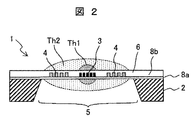
- FIG. 2 is a cross-sectional view of the sensor element illustrated in FIG. 1.
- It is a drive circuit diagram of a sensor element according to an embodiment of the present invention.
- It is a resistance circuit diagram which shows the structure of the comparative example with this invention.
- It is a resistance circuit diagram of the sensor apparatus which concerns on one Example of this invention.
- It is a figure for demonstrating the effect
- It is sectional drawing of the resistance circuit which concerns on one Example of this invention.
- It is a top view of a resistance circuit concerning one example of the present invention.
- It is a top view of a resistance circuit concerning one example of the present invention.
- the present invention is applied to a gas concentration sensor device that measures intake air humidity of an automobile engine as an example of a sensor device.
- the physical quantity (environmental parameter) to be detected by the sensor device of this embodiment is a change in gas concentration, and can be used for measurement of, for example, hydrogen concentration.
- the intake humidity to be measured by the sensor device of the present embodiment is measured by detecting a change in the thermal conductivity of the gas due to the gas concentration.
- a change in thermal conductivity is detected from a change in the amount of heat released from the heater formed in the sensor element. Since the change in the thermal conductivity of the gas due to the concentration of the gas is minute, a highly accurate drive circuit is required for detecting the change in the heat radiation amount of the heater and for controlling the temperature of the heater. In such a sensor device, the configuration of the present invention is required. The effect by is high.
- FIG. 1 shows a plan view of a sensor element 1 of a gas concentration sensor device according to this embodiment.
- the sensor element 1 has a substrate 2 made of single crystal silicon. A cavity 5 is formed in the substrate 2, and the cavity 5 is covered with a thin film support 6.
- the thin film support 6 is provided with a detection heater 3 and a compensation heater 4.
- the compensation heater 4 is arranged so as to surround the detection heater 3.
- the detection heater 3 and the compensation heater 4 are formed as a resistance pattern extending along the plane of the thin film support 6 and having a plurality of folded portions.
- the detection heater 3 and the compensation heater 4 include electrodes 7a, 7b, 7c, and 7d formed on the substrate 2 for connection to the drive circuit 30 (see FIG. 3).
- FIG. 2 is a view showing a II-II section of FIG.
- the sensor element 1 includes a substrate 2 made of single crystal silicon.
- the substrate 2 includes a cavity 5.
- the thin film support 6 is laminated on the upper surface of the substrate 2.
- the thin film support 6 is composed of insulating layers 8a and 8b, and is provided such that the detection heater 3 and the compensation heater 4 are interposed between the insulation layers 8a and 8b. It is supported by the insulating layers 8a and 8b.
- the detection heater 3 is held at the temperature Th1 by controlling the current flowing through the detection heater 3.
- the compensation heater 4 is maintained at the temperature Th2 by controlling the current flowing through the compensation heater 4.
- the temperature Th1 is about 500 ° C.
- the temperature Th2 is about 300 ° C.
- the compensation heater 4 is used to maintain the periphery of the detection heater 3 at a constant temperature higher than the environmental temperature. The influence of environmental temperature changes is eliminated. Thereby, it is possible to directly detect the humidity from the change in the heat radiation amount of the detection heater 3.
- the detection heater 3 and the compensation heater 4 for example, platinum (Pt), tantalum (Ta), molybdenum (Mo), silicon (Si), or the like is selected as a material that is stable at a high temperature (a material having a high melting point).
- platinum (Pt), tantalum (Ta), molybdenum (Mo), silicon (Si), or the like is selected as a material that is stable at a high temperature (a material having a high melting point).
- silicon oxide (SiO2) and silicon nitride (Si3N4) are selected in a single layer or a laminated structure.
- a resin material such as polyimide, ceramic, glass, or the like can be selected in a single layer or a laminated configuration.
- aluminum (Al) or the like is selected as the electrodes 7a, 7b, 7c, and 7d.
- the sensor element 1 is formed by using a semiconductor microfabrication technique using photolithography or an anisotropic etching technique.
- the cavity 5 is formed by processing the single crystal silicon substrate 2 using anisotropic etching or isotropic etching.
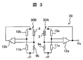
- FIG. 3 shows a driving circuit of the gas concentration sensor device in the present embodiment.
- the sensor device includes the sensor element 1 shown in FIG. 1 and the drive circuit 30 shown in FIG.
- the drive circuit 30 includes a bridge circuit 30A that controls heating of the detection heater 3, and a bridge circuit 30B that controls heating of the compensation heater 4.
- the bridge circuit 30A including the detection heater 3 includes a series circuit (first series circuit) in which a reference resistor 9a is electrically connected in series to the detection heater 3, and a resistor 10a and a resistor 11a electrically connected in series. It consists of a series circuit (second series circuit).
- the potential at the connection between the detection heater 3 and the reference resistor 9a (first potential) and the potential at the connection between the resistors 10a and 11a (second potential) are input to the differential amplifier 12a.
- the differential amplifier 12a outputs a voltage or current corresponding to the difference in input voltage (difference voltage between the first potential and the second potential).
- the output of the differential amplifier 12a is connected between the detection heater 3 of the bridge circuit 30A and the resistor 10a, and is fed back as a heating current of the detection heater 3.
- the resistance values of the resistor 10a and the resistor 11a are set to 10 times or more the resistance value of the detection heater 3. As a result, most of the current supplied from the differential amplifier 12a flows to the detection heater 3, and the detection heater 3 can be efficiently heated.
- the detection heater 3 Since the resistance value of the detection heater 3 changes depending on the temperature, the detection heater 3 can be held at a constant temperature by performing feedback control so that the resistance ratio with the reference resistor 9a is constant.
- a series circuit in which the reference resistor 9b is electrically connected in series to the compensation heater 4, and a resistor 10b and a resistor 11b are electrically connected in series. It consists of a series circuit (fourth series circuit).
- the potential at the connection between the compensation heater 4 and the reference resistor 9b (third potential) and the potential at the connection between the resistor 10ab and the resistor 11b (fourth potential) are input to the differential amplifier 12b.
- the differential amplifier 12b outputs a voltage or current corresponding to the difference in input voltage (difference voltage between the third potential and the fourth potential).
- the output of the differential amplifier 12b is connected between the compensation heater 4 of the bridge circuit 30B and the resistor 10b, and is fed back as a heating current of the compensation heater 4.
- the resistance values of the resistor 10b and the resistor 11b are set to 10 times or more the resistance value of the compensation heater 4. As a result, most of the current supplied from the differential amplifier 12b flows to the compensation heater 4, and the compensation heater 4 can be efficiently heated.
- the compensation heater 4 Since the resistance value of the compensation heater 4 changes depending on the temperature, the compensation heater 4 can be held at a constant temperature by feedback control so that the resistance ratio with the reference resistor 9b is constant.
- the reference resistors 9a and 9b, resistors 10a and 10b, resistors 11a and 11b, and differential amplifier circuits 12a and 12b are integrated on a semiconductor chip.
- the ratio between the resistance value of the resistor 10a and the resistance value of the resistor 11a needs to be constant.
- the ratio of the resistance value of the resistor 10b and the resistance value of the resistor 11b needs to be constant.
- the resistor 10a and the resistor 11a are formed on the semiconductor chip using the same material and in the same process.
- the resistor 10b and the resistor 11b are formed on the semiconductor chip by using the same material and in the same process.
- the resistance change rates of the resistors 10a and 11a are the same, and the resistance change rates of the resistors 10b and 11b are Therefore, the ratio between the resistance value of the resistor 10a and the resistance value of the resistor 11a and the ratio between the resistance value of the resistor 10a and the resistance value of the resistor 11a are kept constant.
- the drive circuit 30 operates so that the ratio between the resistance value of the reference resistor 9a and the resistance value when the detection heater 3 is heated (during driving) is constant. Then, when the resistance value of the reference resistor 9a varies depending on the environmental temperature, the temperature of the detection heater 3 changes so that the resistance ratio with the reference resistor 9a becomes constant. When the temperature of the detection heater 3 changes, the heating power changes and a measurement error occurs. Further, since the ratio of the resistance value of the reference resistor 9b and the resistance value when the compensation heater 4 is heated (during driving) is constant, if the resistance value of the reference resistor 9b varies depending on the environmental temperature, the reference value The temperature of the compensation heater 4 changes so that the resistance ratio with the resistor 9b is constant. Accordingly, the reference resistors 9a and 9b are required to have a small resistance temperature change due to the environmental temperature.
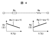
- FIG. 4 shows a configuration of a resistance circuit in a comparative example with the present invention.
- a resistor Rp made of a resistance material having a positive resistance temperature coefficient and a resistor Rn made of a negative resistance material are formed in a series circuit. Connect and form.
- the resistance temperature coefficient of the resistor Rp is ⁇ p and the resistance temperature coefficient of the resistor Rn is ⁇ n
- the resistor Rp and the resistor Rn are formed of different materials, the manufacturing process is different, and the resistance value (Rp) of the resistor Rp and the resistance value (Rn) of the resistor Rn are unrelated to each other. Therefore, a temperature coefficient of resistance corresponding to the variation in the resistance ratio Rp / Rn occurs.
- the present embodiment includes the following resistance circuit.
- FIG. 5 shows a resistance circuit as a reference resistance to which the present invention is applied.
- the resistance circuit 9 of the present invention includes a series circuit (first resistance circuit) Rs composed of a resistance (second resistance element) Rp1 having a positive resistance temperature coefficient and a negative resistance (first resistance element) Rn1, and a resistance temperature coefficient.
- Reference resistors 9a and 9b are configured by including a parallel circuit (second resistor circuit) Rc including a positive resistor (fourth resistor element) Rp2 and a negative resistor (third resistor element) Rn2.
- the resistors Rp1 and Rp2 are formed using the same resistance material and in the same process.
- the resistors Rn1 and Rn2 are formed using the same resistance material and in the same process. That is, the resistors Rp1 and Rp2 are simultaneously patterned by etching a resistance thin film having a positive resistance temperature coefficient.
- the resistance value of the resistor Rp1 and the resistance value of the resistor Rp2 simultaneously vary, and the ratio (resistance ratio) between the resistance value of the resistor Rp1 and the resistance value of the resistor Rp2 is maintained. .
- the resistors Rn1 and Rn2 are simultaneously formed by etching a resistance thin film having a negative resistance temperature coefficient.
- the resistor Rp1 and the resistor Rp2 are formed by the same process on the same layer of the stacked layers. Further, the resistor Rn1 and the resistor Rn2 are formed by the same process on the same layer of the stacked layers.
- the resistance circuit 9 of the present embodiment is obtained by connecting the series circuit Rs and the parallel circuit Rc.
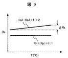
- FIG. 6 shows temperature characteristics when variation occurs in the resistance ratio between the resistor Rn1 and the resistor Rp1 in the combined resistor Rs of the series circuit portion.
- the resistance temperature coefficient ⁇ n of the resistor Rn1 and the resistance temperature coefficient ⁇ p of the Rp1 use resistance materials having the same absolute value but different signs.
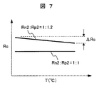
- FIG. 7 shows temperature characteristics when the resistance ratio between the resistor Rn2 and the resistor Rp2 varies in the combined resistor Rc of the parallel circuit section.
- the resistance temperature coefficient ⁇ n of the resistor Rn2 and the resistance temperature coefficient ⁇ p of the resistor Rp2 are examples using resistance materials having the same absolute value but different signs.
- the series circuit Rs shown in FIG. 6 and the parallel circuit Rc shown in FIG. 7 have positive and negative temperature dependences caused by increasing the resistance of materials having a positive resistance temperature coefficient (Rp1, Rp2).
- Rp1, Rp2 a positive resistance temperature coefficient
- the series circuit Rs the temperature dependence of the resistance on the high resistance side of the two resistances appears, so that a positive resistance temperature change occurs when Rp1 becomes a high resistance.
- the parallel circuit Rc the temperature dependency of the resistance on the low resistance side of the two resistances appears, so that a negative resistance temperature change occurs conversely. For this reason, the series circuit Rs and the parallel circuit Rc differ in the temperature dependence of the combined resistances Rs and Rc when the temperature changes.
- the absolute value of the resistance temperature coefficient ⁇ n of the resistors Rn1 and Rn2 and the absolute value of the resistance temperature coefficient ⁇ p of the resistors Rp1 and Rp2 are used is described. If the value and the absolute value of the resistance temperature coefficient ⁇ p are different, the resistance ratio between the resistance Rn1 and the resistance Rp1 may be adjusted as appropriate. The absolute value of the resistance temperature coefficient ⁇ n and the absolute value of the resistance temperature coefficient ⁇ p are the same. There is no need.
- the combined resistance value (Rs) of the series circuit Rs and the combined resistance value (Rc) of the parallel resistor Rc are substantially the same.
- the combined resistance value Rs and the combined resistance value Rc include an error due to processing variation or the like, or a difference between the resistance values Rs and Rc intentionally provided within a range in which the object of the present invention can be achieved.
- the combined resistance value (Rs) and the combined resistance value (Rc) are considered to be substantially the same.
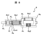
- FIG. 8 and 9 show the specific structure of the resistor circuit 9 of this embodiment.
- FIG. 8 shows a planar structure
- FIG. 9 shows a cross-sectional structure.
- a series circuit Rs composed of polycrystalline silicon Rn1 having a negative resistance temperature coefficient and polycrystalline silicon Rp1 having a positive resistance temperature coefficient, polycrystalline silicon Rn2 having a negative resistance temperature coefficient, and polycrystalline silicon Rp1 having a positive resistance temperature coefficient
- a parallel circuit Rc comprising: Each resistor is connected to the aluminum wiring AL by a contact Cont.
- the resistance temperature coefficient of polycrystalline silicon is determined to be positive or negative depending on the impurity concentration.
- the resistor Rn1 and the resistor Rn2 are formed in the same layer by the same process.
- the resistors Rp1 and Rp2 are also formed in the same layer and in the same process.
- the resistor Rn1 and the resistor Rp1 or the resistor Rn2 and the resistor Rp2 have different resistance temperature coefficients and are formed by different processes.
- the resistor Rn1 and the resistor Rp1 are formed in the same layer, but may be formed in different layers.
- the resistor Rn2 and the resistor Rp2 are formed in the same layer, but may be formed in different layers.
- a diffused resistor in which a silicon substrate is doped with impurities can be used.
- a silicide resistor or a metal resistor can also be used as a diffused resistor in which a silicon substrate is doped with impurities.
- Polycrystalline silicon has less variation in resistivity than these resistive materials. Therefore, the resistance ratio between the resistor Rn1 and the resistor Rn2 and the resistance ratio between the resistor Rp1 and the resistor Rp2 can be matched more, and the effect of the present invention can be enhanced.
- the sensor device 1 used in a harsh environment such as an automobile engine needs to reduce the influence of mechanical strain in addition to temperature change.
- a resistance change due to the piezo effect (hereinafter referred to as piezoresistance change) occurs in the resistance formed on the semiconductor chip.
- Such mechanical strain is generated not only by the expansion and thermal contraction due to the temperature of the semiconductor chip but also by the expansion and contraction of the support material on which the semiconductor chip is installed. Therefore, when the environmental temperature in which the sensor device 1 is used changes, a piezoresistance change occurs in addition to the resistance temperature change.
- the piezoresistance coefficient of semiconductors differs depending on the conductivity type of silicon. For example, in N-type silicon doped with phosphorus as an impurity, the resistance value decreases when tension is applied along the direction of current flowing through the resistor. On the other hand, in the P-type silicon doped with boron as an impurity, the resistance value increases. Therefore, the resistance change due to the distortion of the reference resistor can be reduced by combining silicon materials having different conductivity types.
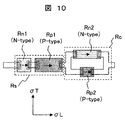
- FIG. 10 shows a specific example of the reference resistance in which the piezoresistance change is reduced.
- the resistors Rn1 and Rn2 use N-type polycrystalline silicon, and the resistors Rp1 and Rp2 use P-type polycrystalline silicon. Other configurations are the same as those in the first embodiment.
- the resistance value of the resistor Rn1 decreases and the resistance value of the resistor Rp1 increases in the resistor Rn1 and the resistor Rp1 constituting the series circuit (first resistor circuit) Rs. To do.
- the resistance value of the resistor Rn2 decreases and the resistance value of the resistor Rp2 increases.
- the piezoresistance change of the resistor Rn1 and the piezoresistance change of the resistor Rp1 cancel each other's resistance change.
- the piezoresistance change of the resistor Rn2 and the piezoresistance change of the resistor Rp2 work so as to cancel each other's resistance change. Therefore, in this embodiment, the influence of the piezoresistance change due to the stress ⁇ L and the stress ⁇ T is suppressed, and the change in the combined resistance value of the resistance circuit 9 is suppressed.
- the resistance circuit 9 of the present embodiment has the series circuit Rs and the parallel circuit Rc as in the first embodiment, and has the same operational effects as the first embodiment.
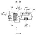
- FIG. 11 shows another specific example of the reference resistance in which the change in piezoresistance is reduced.
- the resistors Rn1, Rn2, Rp1, and Rp2 are all made of N-type polycrystalline silicon having the same conductivity type.
- the direction of current flowing in the resistors Rn1 and Rp1 constituting the series circuit Rs (y direction) and the direction of current flowing in the resistors Rn2 and Rp2 constituting the parallel circuit Rc (x direction) are orthogonal to each other. It is patterned as follows. Other configurations are the same as those in the first and second embodiments.
- the arrangement of the resistors Rn1 and Rp1 constituting the series circuit Rs is different from those in the first and second embodiments. That is, the wiring 13 connecting the resistor Rn1 and the resistor Rp1 is folded back, and the direction of the current flowing through the resistor Rn1 and the direction of the current flowing through the resistor Rp1 are parallel and different in direction by 180 degrees.
- the first resistance element Rn1, the second resistance element Rp1, the third resistance element Rn2, and the fourth resistance element Rp2 are arranged so that the directions of the currents flowing through the first and second resistance elements Rn1, Rp1, Rp1, Rp2, and Rp2 are orthogonal to each other.
- the wiring 13 (see FIG. 8) connected to the resistors Rn1 and Rp1 is formed in a straight line.
- the wiring 13 shown in FIG. A folded configuration may be used as shown.
- the resistors Rn1, Rp1, Rn2, and Rp2 constituting the reference resistor are combined with resistors (N-type resistors) Rn1 and Rn2 having different conductivity types and resistors (P-type resistors) Rp1 and Rp2.
- the change in the reference resistance due to the distortion caused by the change in the environmental temperature is reduced by the configuration and the configuration in which the resistances Rn1, Rp1 and the resistances Rn2, Rp2 of the same conductivity type are combined so that the directions of the flowing currents are different by 90 degrees. be able to.
- this invention is not limited to each above-mentioned Example, Various modifications are included.
- the above-described embodiments have been described in detail for easy understanding of the present invention, and are not necessarily limited to those having all the configurations.
- a part of the configuration of one embodiment can be replaced with the configuration of another embodiment, and the configuration of another embodiment can be added to the configuration of one embodiment.
Landscapes
- Physics & Mathematics (AREA)
- Engineering & Computer Science (AREA)
- Chemical & Material Sciences (AREA)
- General Physics & Mathematics (AREA)
- Microelectronics & Electronic Packaging (AREA)
- Immunology (AREA)
- Electrochemistry (AREA)
- Biochemistry (AREA)
- General Health & Medical Sciences (AREA)
- Life Sciences & Earth Sciences (AREA)
- Health & Medical Sciences (AREA)
- Pathology (AREA)
- Analytical Chemistry (AREA)
- Chemical Kinetics & Catalysis (AREA)
- Electromagnetism (AREA)
- Fluid Mechanics (AREA)
- Ceramic Engineering (AREA)
- Semiconductor Integrated Circuits (AREA)
- Measuring Volume Flow (AREA)
- Investigating Or Analyzing Materials By The Use Of Electric Means (AREA)
Abstract
本発明の目的は、温度変化による特性変化を低減することができるセンサ装置を提供することにある。 物理量に応じて抵抗値が変化する検出抵抗体と前記検出抵抗体と比較される基準抵抗9とを備えたセンサ装置において、基準抵抗9は、抵抗温度係数が正である第1抵抗素子Rn1と抵抗温度係数が負である第2抵抗素子Rp1とを電気的に接続した第1抵抗回路Rsと、抵抗温度係数が正である第3抵抗素子Rn2と抵抗温度係数が負である第4抵抗素子Rp2とを電気的に接続した第2抵抗回路Rcと、を電気的に接続して構成され、第1抵抗回路Rsは、合成抵抗値が温度変化に対して正又は負のいずれかの側に第1のずれを生じるように構成され、第2抵抗回路Rcは、合成抵抗値が前記温度変化に対して、前記第1のずれが生じる正又は負のいずれかの側とは逆側に第2のずれを生じるように構成される。
Description
本発明は、抵抗回路を備えたセンサ装置に係り、特に抵抗値の温度依存性を低減可能な抵抗回路を備えたセンサ装置に関する。
近年、センサ装置の小型化の要求に対応するためにセンサ装置の集積化が進んでいる。例えば、自動車用の内燃機関に使われるセンサ装置においては、吸入空気の流量、湿度、圧力および温度などの環境パラメータの中から複数の環境パラメータを計測することができるようにした複合センサ装置が要求されている。これらの環境パラメータを計測する複数のセンサ素子とLSIなどの回路部品とを一体化するためには、センサ素子および回路部品の小型化や部品数の削減が必要である。
さらにセンサ装置の一例として、センサ素子の駆動回路に基準抵抗を用いたブリッジ回路を用いたものがある。この基準抵抗は、温度による抵抗値変化が小さいことが求められる。従来は、基準抵抗として高精度な抵抗器を用いたり、抵抗トリミングなどにより抵抗器の抵抗値を調整したりしていたが、この場合、部品コストの増加や設置スペースの確保が課題になる。一方、チップ抵抗器の代替となる基準抵抗をLSIに形成することにより部品数を削減することができる。しかし、LSIに形成できる抵抗素子は抵抗値の温度変化(以下、抵抗温度変化という)が大きいという問題がある。センサ素子の駆動回路の基準抵抗に抵抗温度変化があると、センサ装置の温度変化によって計測誤差が発生する。特に、センサ素子のブリッジ回路に使用する基準抵抗は、センサ素子の微少な抵抗変化をセンサ装置の温度変化によらず正確に検出するために、温度依存性を低減する必要がある。
特開2015-50549号公報(特許文献1)には、センサ装置に用いられる発振回路の発振周波数の温度依存性を低減する技術が開示されている。このセンサ装置はセンサ信号を調整して出力する半導体チップを備え、半導体チップはA/Dコンバータ、デジタル演算手段およびD/Aコンバータへ発振周波数を付与する発振回路を備える。発振回路において発振周波数を制御する抵抗器は、正温度係数抵抗器と負温度係数抵抗器とを組み合わせて設けられる。具体的には、正温度係数を有する複数の半導体抵抗と負温度係数を有する複数のコンタクト抵抗とを組み合わせ、半導体抵抗およびコンタクト抵抗の使用個数および使用個数の比率を調整して抵抗器全体の温度特性をフラット化する(要約参照)。さらに具体的には、半導体抵抗およびコンタクト抵抗は直列接続、並列接続、或いは直列接続と並列接続とを組み合わせて、接続される(段落0022参照)。
例えば内燃機関の吸気通路の環境パラメータ(物理量)を測定する気体センサ装置は、走行環境の変化やエンジン発熱により、センサ装置が置かれる環境の温度範囲が広く、-40℃から+125℃においてセンサ性能を満たす必要がある。そのため、抵抗器の温度変化が大きくなり、広範囲の温度環境において抵抗温度変化の小さい抵抗器が必要になる。また、センサ素子の抵抗変化を検出するブリッジ回路の基準抵抗として用いる場合、微小な基準抵抗の抵抗変化が計測精度に影響を与えるため、抵抗温度変化の小さい抵抗器が必要になる。
特許文献1の抵抗器は、正温度係数の抵抗材料からなる半導体抵抗と負温度係数の抵抗材料からなるコンタクト抵抗とを用いることで、半導体抵抗に生じる抵抗温度変化とコンタクト抵抗に生じる抵抗温度変化とを相殺している。この相殺効果を高めるためには半導体抵抗の抵抗値とコンタクト抵抗の抵抗値が最適な比率になっている必要があり、特許文献1の抵抗器では、半導体抵抗の個数とコンタクト抵抗の個数との比率が温度特性をフラット化するように予め調整されている。
しかしながら、製造ばらつきにより各々の抵抗値にばらつきが生じるため半導体抵抗の抵抗値とコンタクト抵抗の抵抗値との比率は設計値通りの比率にならない。抵抗値の比率にばらつきが発生するとどちらかの抵抗の抵抗温度変化が強まり相殺効果が低下する。例えば、正の温度係数を持つ抵抗が設計値より高い抵抗値で製造された場合、全体の合成抵抗には正の温度係数が生じる。逆に、負の温度係数を持つ抵抗が設計値より高抵抗値で製造された場合、全体の合成抵抗には負の温度係数が生じる。
したがって、2種の抵抗材料を組み合わせると2種の抵抗値バランスのばらつきによって、抵抗器の合成抵抗には正負ランダムな抵抗温度係数が生じる。そして、抵抗器に生じる抵抗温度係数は、センサ装置の特性を変化させ、センサ装置の計測精度に影響を与える。
本発明の目的は、温度変化による特性変化を低減することができるセンサ装置を提供することにある。
上記目的を達成するために、本発明のセンサ装置は、
物理量に応じて抵抗値が変化する検出抵抗体と、前記検出抵抗体と比較される基準抵抗と、を備え、前記検出抵抗体の抵抗値の変化に基づいて前記物理量を計測するセンサ装置において、
前記基準抵抗は、抵抗温度係数が正である第1抵抗素子と抵抗温度係数が負である第2抵抗素子とを電気的に接続した第1抵抗回路と、抵抗温度係数が正である第3抵抗素子と抵抗温度係数が負である第4抵抗素子とを電気的に接続した第2抵抗回路と、を電気的に接続して構成され、
前記第1抵抗回路は、合成抵抗値が温度変化に対して正又は負のいずれかの側に第1のずれを生じるように構成され、
前記第2抵抗回路は、合成抵抗値が前記温度変化に対して、前記第1のずれが生じる正又は負のいずれかの側とは逆側に第2のずれを生じるように構成される。
本発明によれば、温度変化によるセンサ装置の特性変化を低減することができ、温度変化の影響を受け難い高精度なセンサ装置を提供することができる。上記した以外の課題、構成及び効果は、以下の実施形態の説明により明らかにされる。
以下で説明する実施例は、センサ装置の一例として自動車エンジンの吸気湿度を計測する気体濃度センサ装置に本発明を適用したものである。本実施例のセンサ装置の検出対象とする物理量(環境パラメータ)は気体の濃度変化であり、例えば水素濃度などの計測にも用いることができる。
本実施例のセンサ装置が計測対象とする吸気湿度は、気体の濃度による気体の熱伝導率変化を検出することにより計測される。熱伝導率の変化はセンサ素子に形成したヒータの放熱量変化から検出する。気体の濃度による気体の熱伝導率変化は微小であることから、ヒータの放熱量変化の検出およびヒータの温度制御において高精度な駆動回路が要求され、このようなセンサ装置においては本発明の構成による効果が高い。
[実施例1]
図1に本実施例における気体濃度センサ装置のセンサ素子1の平面図を示す。
図1に本実施例における気体濃度センサ装置のセンサ素子1の平面図を示す。
センサ素子1は、単結晶シリコンで形成された基板2を有している。基板2には、空洞部5が形成されており、空洞部5は薄膜支持体6によって覆われている。この薄膜支持体6には、検出ヒータ3と補償ヒータ4とが敷設される。補償ヒータ4は検出ヒータ3の周囲を取り巻くように配置されている。検出ヒータ3および補償ヒータ4は、薄膜支持体6の平面に沿って延在し、複数の折り返し部を有する抵抗パターンとして形成される。検出ヒータ3および補償ヒータ4は、駆動回路30(図3参照)との接続のために基板2上に形成された電極7a、7b、7cおよび7dを備える。
図2は、図1のII-II断面を示す図である。
センサ素子1は単結晶シリコンで形成された基板2を備える。基板2は空洞部5を備える。薄膜支持体6は基板2の上面に積層される。薄膜支持体6は絶縁層8a,8bから成り、これらの絶縁層8aと絶縁層8bとの間に、検出ヒータ3および補償ヒータ4が介在するように設けられ、検出ヒータ3および補償ヒータ4は絶縁層8a,8bに支持されている。
図2を用いてセンサ素子1の動作について説明する。
検出ヒータ3は、検出ヒータ3に流れる電流を制御することによって、温度Th1に保持される。また補償ヒータ4は、補償ヒータ4に流れる電流を制御することによって、温度Th2に保持される。例えば温度Th1は500℃程度であり、温度Th2は300℃程度である。センサ素子1が置かれる雰囲気の気体濃度が変化すると気体の熱伝導率が変化し、検出ヒータ3の放熱量が変わる。この放熱量の変化から気体の濃度を検出する。
センサ素子1を設置する環境温度は自動車の走行環境やエンジンの運転状態に応じて変動するが、補償ヒータ4を用いて検出ヒータ3の周辺を環境温度よりも高い一定温度に保持することで、環境温度変化の影響を排除している。これにより、検出ヒータ3の放熱量の変化から湿度を直接検出することができる。
検出ヒータ3および補償ヒータ4としては、高温において安定な材料(高い融点を有する材料)として、例えば、白金(Pt)、タンタル(Ta)、モリブデン(Mo)またはシリコン(Si)等が選定され、絶縁層8a,8bとしては酸化シリコン(SiO2)と窒化シリコン(Si3N4)が単層あるいは積層構成にて選定される。また、絶縁層8a,8bとして、ポリイミドなどの樹脂材料やセラミックまたはガラスなどを単層あるいは積層構成にて選定することもできる。また、電極7a,7b,7c,7dとしては、アルミニウム(Al)等が選定される。
センサ素子1は、フォトリソグラフィーを利用した半導体微細加工技術または異方性エッチング技術を用いて形成される。空洞部5は、単結晶シリコン基板2を異方性エッチングや等方性エッチングなどを用いて加工することにより形成される。
図3は、本実施例における気体濃度センサ装置の駆動回路を示す。
本実施例に係るセンサ装置は図1に示すセンサ素子1と図3に示す駆動回路30とを備えて構成される。駆動回路30は、検出ヒータ3を加熱制御するブリッジ回路30Aと、補償ヒータ4を加熱制御するブリッジ回路30Bとから成る。
検出ヒータ3が含まれるブリッジ回路30Aは、検出ヒータ3に基準抵抗9aを電気的に直列に接続した直列回路(第1直列回路)と、抵抗10aと抵抗11aとを電気的に直列に接続した直列回路(第2直列回路)から成る。検出ヒータ3と基準抵抗9aとの接続部の電位(第1電位)と、抵抗10aと抵抗11aとの接続部の電位(第2電位)とは差動増幅器12aに入力される。差動増幅器12aは、入力電圧の差(第1電位と第2電位との差電圧)に応じた電圧、または電流を出力する。差動増幅器12aの出力はブリッジ回路30Aの検出ヒータ3と抵抗10aとの間に接続され、検出ヒータ3の加熱電流としてフィードバックされる。
抵抗10aおよび抵抗11aの抵抗値は検出ヒータ3の抵抗値の10倍以上に設定する。これにより差動増幅器12aから供給される電流の多くは検出ヒータ3に流れ、検出ヒータ3を効率よく加熱することができる。
検出ヒータ3は温度により抵抗値が変化するため、基準抵抗9aとの抵抗比が一定となるようにフィードバック制御することにより一定温度に保持することができる。
補償ヒータ4が含まれるブリッジ回路30Bは、補償ヒータ4に基準抵抗9bを電気的に直列に接続した直列回路(第3直列回路)と、抵抗10bと抵抗11bとを電気的に直列に接続した直列回路(第4直列回路)から成る。補償ヒータ4と基準抵抗9bとの接続部の電位(第3電位)と、抵抗10ab抵抗11bとの接続部の電位(第4電位)とは差動増幅器12bに入力される。差動増幅器12bは、入力電圧の差(第3電位と第4電位との差電圧)に応じた電圧、または電流を出力する。差動増幅器12bの出力はブリッジ回路30Bの補償ヒータ4と抵抗10bとの間に接続され、補償ヒータ4の加熱電流としてフィードバックされる。
抵抗10bおよび抵抗11bの抵抗値は補償ヒータ4の抵抗値の10倍以上に設定する。これにより差動増幅器12bから供給される電流の多くは補償ヒータ4に流れ、補償ヒータ4を効率よく加熱することができる。
補償ヒータ4は温度により抵抗値が変化するため、基準抵抗9bとの抵抗比が一定となるようにフィードバック制御することにより一定温度に保持することができる。
基準抵抗9a,9b、抵抗10a,10b、抵抗11a,11bおよび差動増幅回路12a,12bは、半導体チップに集積化して設ける。
抵抗10aの抵抗値と抵抗11aの抵抗値との比は一定であることが必要である。また、抵抗10bの抵抗値と抵抗11bの抵抗値との比は一定であることが必要である。このためには、抵抗10aと抵抗11aとは同一材料を用いて且つ同じプロセスで半導体チップに形成する。また、抵抗10bと抵抗11bとは同一材料を用いて且つ同じプロセスで半導体チップに形成する。こうすることで、抵抗10a,11aおよび抵抗10b,11bに抵抗温度変化が発生した場合においても、抵抗10aと抵抗11aとの抵抗変化率は一致し、抵抗10bと抵抗11bとの抵抗変化率は一致するため、抵抗10aの抵抗値と抵抗11aの抵抗値との比および抵抗10aの抵抗値と抵抗11aの抵抗値との比はそれぞれ一定に保たれる。
駆動回路30は、基準抵抗9aの抵抗値と検出ヒータ3の加熱時(駆動時)の抵抗値との比が一定となるように動作している。そうすると、基準抵抗9aの抵抗値が環境温度により変動すると、基準抵抗9aとの抵抗比が一定となるように検出ヒータ3の温度が変化する。検出ヒータ3の温度が変化すると加熱電力が変化し計測誤差が生じる。また、基準抵抗9bの抵抗値と補償ヒータ4の加熱時(駆動時)の抵抗値との比が一定となるように動作することから、基準抵抗9bの抵抗値が環境温度により変動すると、基準抵抗9bとの抵抗比が一定となるように補償ヒータ4の温度が変化する。したがって、基準抵抗9a,9bは環境温度による抵抗温度変化が小さいことが求められる。
図4に本発明との比較例における抵抗回路の構成を示す。
図4の比較例においては、基準抵抗9a,9bを半導体チップに形成する場合、抵抗温度係数が正の抵抗材料からなる抵抗Rpと負の抵抗材料からなる抵抗Rnとを直列回路を成すように接続して形成する。抵抗Rpの抵抗温度係数をαp、抵抗Rnの抵抗温度係数を-αnとすると、抵抗Rnと抵抗Rpとの合成抵抗Rsは、
Rs=Rp(1+αp・T)+Rn(1-αn・T)
=(Rp+Rn)(1+(Rpαp-Rnαn)/(Rp+Rn)・T (1)
となる。式(1)において温度Tの係数をゼロにするためには、
Rp/Rn=αn/αp (2)
となり、抵抗Rpと抵抗Rnとの比を抵抗温度係数αn,αpに合わせて適切に設計することよって温度依存性を相殺する効果が得られる。
Rs=Rp(1+αp・T)+Rn(1-αn・T)
=(Rp+Rn)(1+(Rpαp-Rnαn)/(Rp+Rn)・T (1)
となる。式(1)において温度Tの係数をゼロにするためには、
Rp/Rn=αn/αp (2)
となり、抵抗Rpと抵抗Rnとの比を抵抗温度係数αn,αpに合わせて適切に設計することよって温度依存性を相殺する効果が得られる。
しかし、抵抗Rpと抵抗Rnとは異なる材料で形成されるため、製造プロセスも異なり抵抗Rpの抵抗値(Rp)と抵抗Rnの抵抗値(Rn)とには互いに無関係なばらつきが発生する。したがって、抵抗比Rp/Rnのばらつきに応じた抵抗温度係数が生じる。
この課題に対して、本実施例では以下の抵抗回路を備える。
図5に本発明を適用した基準抵抗としての抵抗回路を示す。
本発明の抵抗回路9は、抵抗温度係数が正の抵抗(第2抵抗素子)Rp1と負の抵抗(第1抵抗素子)Rn1からなる直列回路(第1抵抗回路)Rsと、抵抗温度係数が正の抵抗(第4抵抗素子)Rp2と負の抵抗(第3抵抗素子)Rn2からなる並列回路(第2抵抗回路)Rcとを備え、基準抵抗9a,9bを構成する。
抵抗Rp1と抵抗Rp2とは同一の抵抗材料を用いて且つ同じプロセスで形成する。また、抵抗Rn1と抵抗Rn2とは同一の抵抗材料を用いて且つ同じプロセスで形成する。つまり、抵抗温度係数が正の抵抗薄膜をエッチングすることにより抵抗Rp1と抵抗Rp2とを同時にパターニングし形成する。抵抗薄膜の膜厚に製造ばらつきが生じると、抵抗Rp1の抵抗値と抵抗Rp2の抵抗値とは同時にばらつき、抵抗Rp1の抵抗値と抵抗Rp2の抵抗値との比(抵抗比)は保持される。抵抗Rn1と抵抗Rn2とについても同様に、抵抗温度係数が負となる抵抗薄膜をエッチングすることにより同時に形成される。
すなわち本実施例では、抵抗Rp1と抵抗Rp2とは積み重なった複数層の中の同じ層の膜に同じプロセスで形成される。また抵抗Rn1と抵抗Rn2とは積み重なった複数層の中の同じ層の膜に同じプロセスで形成される。
抵抗Rp1,Rp2の抵抗温度係数をαp、抵抗Rn1,Rn2の抵抗温度係数を-αnとすると、抵抗回路9における抵抗Rn1と抵抗Rp1との直列回路の合成抵抗Rsは、
Rs=Rn1(1+αn・T)+Rp1(1-αp・T) (3)
となる。また、抵抗回路9における抵抗Rn2と抵抗Rp2との並列回路の合成抵抗Rcは、
Rc=1/(1/(Rn1(1+αn・T))+1/(Rp1(1-αp・T))) (4)となる。本実施例の抵抗回路9は上記の直列回路Rsと並列回路Rcとを接続したものである。
Rs=Rn1(1+αn・T)+Rp1(1-αp・T) (3)
となる。また、抵抗回路9における抵抗Rn2と抵抗Rp2との並列回路の合成抵抗Rcは、
Rc=1/(1/(Rn1(1+αn・T))+1/(Rp1(1-αp・T))) (4)となる。本実施例の抵抗回路9は上記の直列回路Rsと並列回路Rcとを接続したものである。
以下、本実施例の抵抗回路9の作用および効果を説明する。
図6に、直列回路部の合成抵抗Rsにおいて、抵抗Rn1と抵抗Rp1との抵抗比にばらつきが生じたときの温度特性を示す。ここで、抵抗Rn1の抵抗温度係数αnとRp1の抵抗温度係数αpとは絶対値が等しく符号の正負が異なる特性の抵抗材を用いた例を示す。
図6に示すように、抵抗Rp1と抵抗Rn1との抵抗比が、設計値通りの1:1である場合、抵抗Rn1の抵抗温度変化と抵抗Rp1の抵抗温度変化とが互いに相殺し、温度に対してフラットな特性となる。次に、製造ばらつきによりRp1が1.2倍となった場合、全体の合成抵抗Rsはプラスにシフトすると同時に、温度に対する相殺効果が崩れ、温度変化によってΔRsの抵抗増加が生じる。
図7に、並列回路部の合成抵抗Rcにおいて、抵抗Rn2と抵抗Rp2との抵抗比にばらつきが生じたときの温度特性を示す。ここで、同様に抵抗Rn2の抵抗温度係数αnと抵抗Rp2の抵抗温度係数αpとは絶対値が等しく符号の正負が異なる特性の抵抗材を用いた例を示す。
図7に示すように、抵抗Rp2と抵抗Rn2との抵抗比が、設計値通りの1:1である場合、抵抗Rn2の抵抗温度変化と抵抗Rp2の抵抗温度変化とが互いに相殺し、温度に対してフラットな特性となる。次に、製造ばらつきにより抵抗Rp2が1.2倍となった場合、全体の合成抵抗Rcがプラスにシフトすると同時に、温度に対する相殺効果が崩れ、温度変化によってΔRcの抵抗減少が生じる。
図6に示した直列回路Rsと図7で示した並列回路Rcとは、抵抗温度係数が正の材料(Rp1、Rp2)の高抵抗化により発生する温度依存性が正負で異なる。直列回路Rsでは、2つの抵抗のうち高抵抗側の抵抗の温度依存性が現れるため、Rp1が高抵抗になると正の抵抗温度変化が生じる。一方、並列回路Rcでは、2つの抵抗のうち低抵抗側の抵抗の温度依存性が現れるため、逆に負の抵抗温度変化が生じる。このため、直列回路Rsと並列回路Rcとは、温度変化が生じた場合の合成抵抗Rs,Rcの温度依存性が正負で異なる。
直列回路Rsの合成抵抗値(Rs)と並列回路Rcの合成抵抗値(Rc)とを電気的に直列に接続すると、直列回路Rsの抵抗増加と並列回路Rcの抵抗減少とが互いに相殺する効果が得られる。
上記の例では抵抗Rn1,Rn2の抵抗温度係数αnの絶対値と、抵抗Rp1,Rp2の抵抗温度係数αpの絶対値とが同一の材料を用いた場合について説明したが、抵抗温度係数αnの絶対値と抵抗温度係数αpの絶対値とが異なる場合は適宜、抵抗Rn1と抵抗Rp1との抵抗比を調整すればよく、抵抗温度係数αnの絶対値と抵抗温度係数αpの絶対値とは同一である必要はない。
好ましくは、直列回路Rsの合成抵抗値(Rs)と並列回路Rcの合成抵抗値(Rc)とは、ほぼ同等の抵抗値(Rs=Rc)となるように設計すれば、図6および図7に示したΔRsとΔRcとがより一致するため、抵抗ばらつきにより発生する抵抗温度変化の相殺効果が高まる。
すなわち、直列回路Rsの合成抵抗値(Rs)と並列抵抗Rcの合成抵抗値(Rc)とが実質的に同じである。ここで、合成抵抗値Rsと合成抵抗値Rcとが加工のばらつき等による誤差や、本発明の目的を達成可能な範囲で故意に設けられた各抵抗値Rs,Rcの差を含む場合は、合成抵抗値(Rs)と合成抵抗値(Rc)とは実質的に同じであるとみなされる。
図8および図9に本実施例の抵抗回路9の具体的構造を示す。図8は平面構造、図9は断面構造を示す。
抵抗温度係数が負の多結晶シリコンRn1と抵抗温度係数が正の多結晶シリコンRp1とからなる直列回路Rsと、抵抗温度係数が負の多結晶シリコンRn2と抵抗温度係数が正の多結晶シリコンRp1とからなる並列回路Rcとを電気的に直列に接続した構成である。各々の抵抗はアルミ配線ALとコンタクトContにより接続している。多結晶シリコンの抵抗温度係数は不純物濃度により正負が決定する。
図9の断面構造に示すように、抵抗Rn1と抵抗Rn2とは同一層に同一プロセスで形成される。また、抵抗Rp1と抵抗Rp2とについても同一層に同一プロセスで形成される。抵抗Rn1と抵抗Rp1あるいは抵抗Rn2と抵抗Rp2は、異なる抵抗温度係数であるため異なるプロセスで形成される。図中では抵抗Rn1と抵抗Rp1とは同一層に形成されているが、異なる層に形成されることもある。また抵抗Rn2と抵抗Rp2とは同一層に形成されているが、異なる層に形成されることもある。
また、上記の抵抗材料としては、多結晶シリコンのほか、シリコン基板に不純物をドープした拡散抵抗を用いることができる。シリコン基板に不純物をドープした拡散抵抗としては、シリサイド抵抗または金属抵抗を用いることもできる。多結晶シリコンはこれらの抵抗材料に比べて抵抗率のばらつきが小さい。したがって、抵抗Rn1と抵抗Rn2との抵抗比、抵抗Rp1と抵抗Rp2との抵抗比をより一致させることができ、本発明の効果を高めることができる。
[実施例2]
本発明に係るセンサ素子の基準抵抗の他の実施例を説明する。
本発明に係るセンサ素子の基準抵抗の他の実施例を説明する。
自動車エンジンなどの過酷な環境で使用されるセンサ装置1には、温度変化に加えて機械的な歪の影響を低減する必要がある。駆動回路9を形成した半導体チップに歪が加わると半導体チップに形成した抵抗にピエゾ効果による抵抗変化(以下、ピエゾ抵抗変化という)が生じる。このような機械的歪は半導体チップの温度による膨張および熱収縮のほか、半導体チップを設置した支持材の膨張および収縮によっても発生する。したがって、センサ装置1が使用される環境温度が変化すると、抵抗温度変化に加えてピエゾ抵抗変化が発生する。
半導体のピエゾ抵抗係数はシリコンの導電型によって正負異なる。例えば、不純物としてリンをドープしたN型シリコンでは、抵抗に流れる電流方向に沿って引っ張りを加えると抵抗値が減少する。不純物としてボロンをドープしたP型シリコンでは、逆に抵抗値が増加する。したがって、基準抵抗器の歪による抵抗変化は、導電型の異なるシリコン材料を複合することによって低減できる。
図10に、上記のピエゾ抵抗変化を低減した基準抵抗の具体例を示す。
抵抗Rn1,Rn2はN型多結晶シリコンを用い、抵抗Rp1,Rp2はP型多結晶シリコンを用いている。それ以外の構成は、実施例1と同様に構成される。
抵抗に流れる電流方向に沿った応力σLが加わると、直列回路(第1抵抗回路)Rsを構成する抵抗Rn1および抵抗Rp1においては、抵抗Rn1の抵抗値は減少し、抵抗Rp1の抵抗値は増加する。また並列回路(第2抵抗回路)Rcを構成する抵抗Rn2および抵抗Rp2においては、抵抗Rn2の抵抗値は減少し、抵抗Rp2の抵抗値は増加する。
抵抗に流れる電流方向に交差する応力σTが加わると、直列回路Rsを構成する抵抗Rn1および抵抗Rp1においては、抵抗Rn1の抵抗値は増加し、抵抗Rp1の抵抗値は減少する。また並列回路Rcを構成する抵抗Rn2および抵抗Rp2においては、抵抗Rn2の抵抗値は増加し、抵抗Rp2の抵抗値は減少する。
上述した構成では、導電型の異なる抵抗を複合させることで、応力σLまたは応力σTが加わった場合に、抵抗Rn1のピエゾ抵抗変化と抵抗Rp1のピエゾ抵抗変化とが互いの抵抗変化を打ち消すように働くと共に、抵抗Rn2のピエゾ抵抗変化と抵抗Rp2のピエゾ抵抗変化とが互いの抵抗変化を打ち消すように働く。従って本実施例では、応力σLおよび応力σTによるピエゾ抵抗変化による影響を抑制して、抵抗回路9の合成抵抗値の変化を抑制する。
また本実施例の抵抗回路9は、実施例1と同様に直列回路Rsおよび並列回路Rcを有し、実施例1と同様な作用効果を有する。
[実施例3]
図11に、ピエゾ抵抗変化を低減した基準抵抗のその他の具体例を示す。
図11に、ピエゾ抵抗変化を低減した基準抵抗のその他の具体例を示す。
抵抗Rn1,Rn2,Rp1,Rp2はすべて同じ導電型のN型多結晶シリコンを用いている。また、直列回路Rsを構成する抵抗Rn1,Rp1に流れる電流の方向(y方向)と並列回路Rcを構成する抵抗Rn2,Rp2に流れる電流の方向(x方向)とは、互いに直交する方向を向くようにパターニングしている。それ以外の構成は、実施例1および実施例2と同様に構成される。
上記構造において、図中のx方向に応力が加わると、抵抗Rn1,Rp1の抵抗値は増加し、抵抗Rn2,Rp2の抵抗値は減少する。このように同じ導電型の抵抗Rn1,Rp1と抵抗Rn2,Rp2とを電流の向きが直交するように配置することで、抵抗Rn1,Rp1と抵抗Rn2,Rp2とは互いの抵抗変化を打ち消すように働く。
このために本実施例では、直列回路Rsを構成する抵抗Rn1および抵抗Rp1の配置が、実施例1および実施例2と異なっている。すなわち抵抗Rn1と抵抗Rp1と接続する配線13が折り返され、抵抗Rn1に流れる電流の方向と抵抗Rp1に流れる電流の方向とは平行で且つ180度向きが異なる。
すなわち本実施例では、第1抵抗回路Rsを構成する第1抵抗素子Rn1及び第2抵抗素子Rn2に流れる電流の方向と第2抵抗回路Rcを構成する第3抵抗素子Rn2及び第4抵抗素子Rp2に流れる電流の方向とが直交するように、第1抵抗素子Rn1、第2抵抗素子Rp1、第3抵抗素子Rn2及び第4抵抗素子Rp2が配置される。
なお実施例1では、抵抗Rn1と抵抗Rp1と接続する配線13(図8参照)が直線状に形成されているが、ピエゾ抵抗変化を無視できる場合に、図8に示す配線13を図11に示すように折り返した構成にしてもよい。
上記のように、基準抵抗を構成する抵抗体Rn1,Rp1,Rn2,Rp2を、導電型の異なる抵抗(N型の抵抗)Rn1,Rn2と抵抗(P型の抵抗)Rp1,Rp2とを組み合わせて構成する構成や、同じ導電型の抵抗Rn1,Rp1と抵抗Rn2,Rp2とを、流れる電流の向きが90度異なるように組み合わせる構成によって、環境温度の変化により生じる歪による基準抵抗の変化を低減することができる。
上述した各実施例では、直列抵抗Rs(Rn1、Rp1)と並列抵抗Rc(Rn2、Rp2)とを直列に接続した構成を示したが、これらを並列に接続した構成でも同様の効果が得られる。
なお、本発明は上記した各実施例に限定されるものではなく、様々な変形例が含まれる。例えば、上記した実施例は本発明を分かりやすく説明するために詳細に説明したものであり、必ずしも全ての構成を備えるものに限定されるものではない。また、ある実施例の構成の一部を他の実施例の構成に置き換えることが可能であり、また、ある実施例の構成に他の実施例の構成を加えることも可能である。また、各実施例の構成の一部について、他の構成の追加・削除・置換をすることが可能である。
1…センサ素子、2…基板、3…検出ヒータ、4…補償ヒータ、5…空洞部、6…薄膜支持体、7a~7d…電極、8a,8b…絶縁層、9a,9b…基準抵抗、10a,10b…抵抗、11a,11b…抵抗、12a,12b…差動増幅器、13…配線、30…駆動回路,30A…検出ヒータ3が含まれるブリッジ回路、30B…補償ヒータ4が含まれるブリッジ回路、Rc…並列回路、Rn1,Rp1…直列回路Rsを構成する抵抗体、Rn2,Rp2…並列回路Rcを構成する抵抗体、Rs…直列回路。
Claims (6)
- 物理量に応じて抵抗値が変化する検出抵抗体と、前記検出抵抗体と比較される基準抵抗と、を備え、前記検出抵抗体の抵抗値の変化に基づいて前記物理量を計測するセンサ装置において、
前記基準抵抗は、抵抗温度係数が正である第1抵抗素子と抵抗温度係数が負である第2抵抗素子とを電気的に接続した第1抵抗回路と、抵抗温度係数が正である第3抵抗素子と抵抗温度係数が負である第4抵抗素子とを電気的に接続した第2抵抗回路と、を電気的に接続して構成され、
前記第1抵抗回路は、合成抵抗値が温度変化に対して正又は負のいずれかの側に第1のずれを生じるように構成され、
前記第2抵抗回路は、合成抵抗値が前記温度変化に対して、前記第1のずれが生じる正又は負のいずれかの側とは逆側に第2のずれを生じるように構成されることを特徴とするセンサ装置。 - 請求項1に記載のセンサ装置において、
前記第1抵抗回路は、前記第1抵抗素子と前記第2抵抗素子とが直列に接続された直列回路で構成され、
前記第2抵抗回路は、前記第3抵抗素子と前記第4抵抗素子とが並列に接続された並列回路で構成されることを特徴とするセンサ装置。 - 請求項2に記載のセンサ装置において、
前記第1抵抗素子と前記第3抵抗素子とは、同一層の多結晶シリコン膜により形成され、
前記第2抵抗素子と前記第4抵抗素子とは、同一層の多結晶シリコン膜により形成されることを特徴とするセンサ装置。 - 請求項3に記載のセンサ装置において、
前記基準抵抗は、前記直列回路の合成抵抗値と前記並列回路の合成抵抗値とが実質的に同じであることを特徴とするセンサ装置。 - 請求項3に記載のセンサ装置において、
前記第1抵抗素子と前記第3抵抗素子とは、同一の導電型となる不純物をドープした多結晶シリコンであり、
前記第3抵抗素子と前記第4抵抗素子とは、前記1抵抗素子及び前記第2抵抗素子と異なる導電型の不純物をドープした多結晶シリコンであることを特徴とするセンサ装置。 - 請求項3に記載のセンサ装置において、
前記第1抵抗素子、前記第2抵抗素子、前記第3抵抗素子及び前記第4抵抗素子は、同一の導電型となる不純物をドープした多結晶シリコンであり、
前記第1抵抗回路を構成する前記第1抵抗素子及び前記第2抵抗素子に流れる電流の方向と前記第2抵抗回路を構成する前記第3抵抗素子及び前記第4抵抗素子に流れる電流の方向とが直交するように、前記第1抵抗素子、前記第2抵抗素子、前記第3抵抗素子及び前記第4抵抗素子が配置されることを特徴とするセンサ装置。
Priority Applications (2)
| Application Number | Priority Date | Filing Date | Title |
|---|---|---|---|
| DE112017003438.8T DE112017003438T5 (de) | 2016-08-22 | 2017-07-04 | Sensorvorrichtung |
| US16/325,593 US11047822B2 (en) | 2016-08-22 | 2017-07-04 | Sensor device |
Applications Claiming Priority (2)
| Application Number | Priority Date | Filing Date | Title |
|---|---|---|---|
| JP2016-161626 | 2016-08-22 | ||
| JP2016161626A JP6603633B2 (ja) | 2016-08-22 | 2016-08-22 | センサ装置 |
Publications (1)
| Publication Number | Publication Date |
|---|---|
| WO2018037719A1 true WO2018037719A1 (ja) | 2018-03-01 |
Family
ID=61245859
Family Applications (1)
| Application Number | Title | Priority Date | Filing Date |
|---|---|---|---|
| PCT/JP2017/024425 Ceased WO2018037719A1 (ja) | 2016-08-22 | 2017-07-04 | センサ装置 |
Country Status (4)
| Country | Link |
|---|---|
| US (1) | US11047822B2 (ja) |
| JP (1) | JP6603633B2 (ja) |
| DE (1) | DE112017003438T5 (ja) |
| WO (1) | WO2018037719A1 (ja) |
Cited By (3)
| Publication number | Priority date | Publication date | Assignee | Title |
|---|---|---|---|---|
| CN109831200A (zh) * | 2019-01-08 | 2019-05-31 | 上海华虹宏力半导体制造有限公司 | 电阻电路结构 |
| JP2020035899A (ja) * | 2018-08-30 | 2020-03-05 | ルネサスエレクトロニクス株式会社 | 半導体装置 |
| JP2024077416A (ja) * | 2022-11-28 | 2024-06-07 | ローム株式会社 | オシレータ回路、タイマー回路 |
Families Citing this family (6)
| Publication number | Priority date | Publication date | Assignee | Title |
|---|---|---|---|---|
| CN112585455B (zh) * | 2018-08-10 | 2024-10-29 | Tdk株式会社 | 气体传感器 |
| JP7268333B2 (ja) * | 2018-11-16 | 2023-05-08 | Tdk株式会社 | 歪検出素子および力学量センサ |
| JP2020177393A (ja) * | 2019-04-17 | 2020-10-29 | エイブリック株式会社 | 定電流回路及び半導体装置 |
| JP7508946B2 (ja) | 2020-08-26 | 2024-07-02 | 富士電機株式会社 | 半導体モジュール |
| JP7509054B2 (ja) * | 2021-02-25 | 2024-07-02 | オムロン株式会社 | 熱式センサ |
| DE102023205187A1 (de) | 2023-06-02 | 2024-12-05 | Infineon Technologies Ag | Sensorvorrichtung zur messung einergaskonzentration und verfahren zum bestimmen einer gaskonzentration |
Citations (3)
| Publication number | Priority date | Publication date | Assignee | Title |
|---|---|---|---|---|
| JPS6082949A (ja) * | 1983-10-14 | 1985-05-11 | Sanyo Electric Co Ltd | 電子式湿度計 |
| US5345184A (en) * | 1991-12-16 | 1994-09-06 | Sharp Kabushiki Kaisha | Humidity detection circuit for electronic heat cooking apparatus |
| JP2015050549A (ja) * | 2013-08-30 | 2015-03-16 | 株式会社デンソー | 発振回路 |
Family Cites Families (9)
| Publication number | Priority date | Publication date | Assignee | Title |
|---|---|---|---|---|
| US3728702A (en) * | 1969-12-11 | 1973-04-17 | Matsushita Electric Industrial Co Ltd | Temperature alarm utilizing paired positive and negative coefficient thermistors |
| GB2140615B (en) * | 1983-03-22 | 1987-03-18 | Standard Telephones Cables Ltd | Thermistor composite |
| JPH0653417A (ja) * | 1992-05-19 | 1994-02-25 | Texas Instr Inc <Ti> | 抵抗器回路およびそれを形成する方法 |
| US5748429A (en) * | 1996-09-09 | 1998-05-05 | Honeywell Inc. | Self checking temperature sensing circuit |
| JP2004157024A (ja) * | 2002-11-07 | 2004-06-03 | Omron Corp | 温度検出装置 |
| US6888763B1 (en) * | 2003-02-04 | 2005-05-03 | Advanced Micro Devices, Inc. | Compensated oscillator circuit for charge pumps |
| US7217981B2 (en) * | 2005-01-06 | 2007-05-15 | International Business Machines Corporation | Tunable temperature coefficient of resistance resistors and method of fabricating same |
| KR100697278B1 (ko) * | 2005-01-27 | 2007-03-20 | 삼성전자주식회사 | 저항소자를 가지는 반도체 집적회로 |
| JP6294172B2 (ja) * | 2014-06-30 | 2018-03-14 | 日立オートモティブシステムズ株式会社 | 物理量検出装置 |
-
2016
- 2016-08-22 JP JP2016161626A patent/JP6603633B2/ja not_active Expired - Fee Related
-
2017
- 2017-07-04 DE DE112017003438.8T patent/DE112017003438T5/de not_active Withdrawn
- 2017-07-04 WO PCT/JP2017/024425 patent/WO2018037719A1/ja not_active Ceased
- 2017-07-04 US US16/325,593 patent/US11047822B2/en not_active Expired - Fee Related
Patent Citations (3)
| Publication number | Priority date | Publication date | Assignee | Title |
|---|---|---|---|---|
| JPS6082949A (ja) * | 1983-10-14 | 1985-05-11 | Sanyo Electric Co Ltd | 電子式湿度計 |
| US5345184A (en) * | 1991-12-16 | 1994-09-06 | Sharp Kabushiki Kaisha | Humidity detection circuit for electronic heat cooking apparatus |
| JP2015050549A (ja) * | 2013-08-30 | 2015-03-16 | 株式会社デンソー | 発振回路 |
Cited By (4)
| Publication number | Priority date | Publication date | Assignee | Title |
|---|---|---|---|---|
| JP2020035899A (ja) * | 2018-08-30 | 2020-03-05 | ルネサスエレクトロニクス株式会社 | 半導体装置 |
| JP7015754B2 (ja) | 2018-08-30 | 2022-02-03 | ルネサスエレクトロニクス株式会社 | 半導体装置 |
| CN109831200A (zh) * | 2019-01-08 | 2019-05-31 | 上海华虹宏力半导体制造有限公司 | 电阻电路结构 |
| JP2024077416A (ja) * | 2022-11-28 | 2024-06-07 | ローム株式会社 | オシレータ回路、タイマー回路 |
Also Published As
| Publication number | Publication date |
|---|---|
| JP2018031586A (ja) | 2018-03-01 |
| DE112017003438T5 (de) | 2019-03-28 |
| US20190204251A1 (en) | 2019-07-04 |
| US11047822B2 (en) | 2021-06-29 |
| JP6603633B2 (ja) | 2019-11-06 |
Similar Documents
| Publication | Publication Date | Title |
|---|---|---|
| JP6603633B2 (ja) | センサ装置 | |
| CN101308036B (zh) | 热式流量计 | |
| JP5055349B2 (ja) | 熱式ガスセンサ | |
| CN102004125B (zh) | 热式湿度传感器 | |
| CN101013043B (zh) | 热式流量传感器 | |
| JP5683192B2 (ja) | 熱式流量センサ | |
| CN108369198B (zh) | 气体传感器装置及气体传感器装置的加热电流控制方法 | |
| JP5315304B2 (ja) | 熱式流量計 | |
| CN100437043C (zh) | 物理量传感器 | |
| JP6438706B2 (ja) | センサ装置 | |
| US9232315B2 (en) | Monolithically applied heating elements on saw substrate | |
| US6684693B2 (en) | Heat generation type flow sensor | |
| JP5769043B2 (ja) | 電気素子、集積素子、電子回路及び温度較正装置 | |
| CN113811744B (zh) | 热式传感器装置 | |
| JP2001012985A (ja) | 熱式空気流量センサ及び内燃機関制御装置 | |
| JP5492834B2 (ja) | 熱式流量計 | |
| JP5628236B2 (ja) | 熱式湿度センサ | |
| JP6532810B2 (ja) | 流量センサ |
Legal Events
| Date | Code | Title | Description |
|---|---|---|---|
| 121 | Ep: the epo has been informed by wipo that ep was designated in this application |
Ref document number: 17843207 Country of ref document: EP Kind code of ref document: A1 |
|
| 122 | Ep: pct application non-entry in european phase |
Ref document number: 17843207 Country of ref document: EP Kind code of ref document: A1 |