WO2018021085A1 - 回路基板固定構造、及び電気機器 - Google Patents
回路基板固定構造、及び電気機器 Download PDFInfo
- Publication number
- WO2018021085A1 WO2018021085A1 PCT/JP2017/025876 JP2017025876W WO2018021085A1 WO 2018021085 A1 WO2018021085 A1 WO 2018021085A1 JP 2017025876 W JP2017025876 W JP 2017025876W WO 2018021085 A1 WO2018021085 A1 WO 2018021085A1
- Authority
- WO
- WIPO (PCT)
- Prior art keywords
- circuit board
- case
- screw
- diameter
- inner cylinder
- Prior art date
- Legal status (The legal status is an assumption and is not a legal conclusion. Google has not performed a legal analysis and makes no representation as to the accuracy of the status listed.)
- Ceased
Links
Images




Classifications
-
- H—ELECTRICITY
- H05—ELECTRIC TECHNIQUES NOT OTHERWISE PROVIDED FOR
- H05K—PRINTED CIRCUITS; CASINGS OR CONSTRUCTIONAL DETAILS OF ELECTRIC APPARATUS; MANUFACTURE OF ASSEMBLAGES OF ELECTRICAL COMPONENTS
- H05K7/00—Constructional details common to different types of electric apparatus
- H05K7/14—Mounting supporting structure in casing or on frame or rack
- H05K7/1417—Mounting supporting structure in casing or on frame or rack having securing means for mounting boards, plates or wiring boards
- H05K7/142—Spacers not being card guides
-
- H—ELECTRICITY
- H05—ELECTRIC TECHNIQUES NOT OTHERWISE PROVIDED FOR
- H05K—PRINTED CIRCUITS; CASINGS OR CONSTRUCTIONAL DETAILS OF ELECTRIC APPARATUS; MANUFACTURE OF ASSEMBLAGES OF ELECTRICAL COMPONENTS
- H05K7/00—Constructional details common to different types of electric apparatus
- H05K7/14—Mounting supporting structure in casing or on frame or rack
- H05K7/1422—Printed circuit boards receptacles, e.g. stacked structures, electronic circuit modules or box like frames
- H05K7/1427—Housings
-
- H—ELECTRICITY
- H05—ELECTRIC TECHNIQUES NOT OTHERWISE PROVIDED FOR
- H05K—PRINTED CIRCUITS; CASINGS OR CONSTRUCTIONAL DETAILS OF ELECTRIC APPARATUS; MANUFACTURE OF ASSEMBLAGES OF ELECTRICAL COMPONENTS
- H05K1/00—Printed circuits
- H05K1/02—Details
-
- H—ELECTRICITY
- H05—ELECTRIC TECHNIQUES NOT OTHERWISE PROVIDED FOR
- H05K—PRINTED CIRCUITS; CASINGS OR CONSTRUCTIONAL DETAILS OF ELECTRIC APPARATUS; MANUFACTURE OF ASSEMBLAGES OF ELECTRICAL COMPONENTS
- H05K5/00—Casings, cabinets or drawers for electric apparatus
- H05K5/0026—Casings, cabinets or drawers for electric apparatus provided with connectors and printed circuit boards [PCB], e.g. automotive electronic control units
- H05K5/0047—Casings, cabinets or drawers for electric apparatus provided with connectors and printed circuit boards [PCB], e.g. automotive electronic control units having a two-part housing enclosing a PCB
- H05K5/0052—Casings, cabinets or drawers for electric apparatus provided with connectors and printed circuit boards [PCB], e.g. automotive electronic control units having a two-part housing enclosing a PCB characterized by joining features of the housing parts
-
- H—ELECTRICITY
- H05—ELECTRIC TECHNIQUES NOT OTHERWISE PROVIDED FOR
- H05K—PRINTED CIRCUITS; CASINGS OR CONSTRUCTIONAL DETAILS OF ELECTRIC APPARATUS; MANUFACTURE OF ASSEMBLAGES OF ELECTRICAL COMPONENTS
- H05K5/00—Casings, cabinets or drawers for electric apparatus
- H05K5/0026—Casings, cabinets or drawers for electric apparatus provided with connectors and printed circuit boards [PCB], e.g. automotive electronic control units
- H05K5/0047—Casings, cabinets or drawers for electric apparatus provided with connectors and printed circuit boards [PCB], e.g. automotive electronic control units having a two-part housing enclosing a PCB
- H05K5/006—Casings, cabinets or drawers for electric apparatus provided with connectors and printed circuit boards [PCB], e.g. automotive electronic control units having a two-part housing enclosing a PCB characterized by features for holding the PCB within the housing
-
- H—ELECTRICITY
- H05—ELECTRIC TECHNIQUES NOT OTHERWISE PROVIDED FOR
- H05K—PRINTED CIRCUITS; CASINGS OR CONSTRUCTIONAL DETAILS OF ELECTRIC APPARATUS; MANUFACTURE OF ASSEMBLAGES OF ELECTRICAL COMPONENTS
- H05K2201/00—Indexing scheme relating to printed circuits covered by H05K1/00
- H05K2201/10—Details of components or other objects attached to or integrated in a printed circuit board
- H05K2201/10227—Other objects, e.g. metallic pieces
- H05K2201/10409—Screws
Definitions
- the technology disclosed in this specification relates to a circuit board fixing structure and an electric device.
- a substrate is arranged between the main body case and the lower case, and the substrate is fixed to either the main body case or the lower case.
- An example of this substrate fixing structure is disclosed in Patent Document 1.
- Patent Document 1 a fixing boss is erected on the case body, and a screw is inserted into a screw hole provided for each of the reinforcing plate, the flexible substrate, and the spacer from the reinforcing plate side.
- the reinforcing plate, the flexible substrate, and the spacer are fixed to the case body by screwing in the fixing hole of the boss.
- the screw seat surface presses the reinforcing plate, and the pressing force is directly applied to the flexible substrate stacked on the reinforcing plate. For this reason, in the peripheral portion of the fixing hole into which the screw of the flexible substrate is inserted, there is a risk that distortion or twisting may occur due to the pressing force applied to the portion corresponding to the screw seat surface and the periphery thereof. Since circuit wiring cannot be performed in such a portion of the flexible substrate where distortion or twisting occurs, the mounting area is reduced.
- the technology disclosed in the present specification has been completed based on the above circumstances, and can improve the wiring density of the circuit board without reducing the mounting area of the circuit board. It is an object of the present invention to provide a fixing structure and an electric device using the same.
- a screw having a head having a diameter larger than that of the shaft portion and a shaft portion of the screw are screwed to one end portion of the shaft portion provided with a screw thread.
- An outer cylinder portion having an inner cylinder portion having a threaded hole and a fitting hole having an inner diameter dimension larger than the outer dimension of the inner cylinder portion and fitted to the inner cylinder portion, and one of the outer cylinder portions The other end of the outer cylinder is provided with a contacted portion with which the head of the screw comes into contact with the screw shaft being screwed into the screw hole of the inner cylinder.
- An outer cylinder part having a pressing part, a large-diameter part that does not move relative to the outer peripheral surface of the inner cylinder part, and has a diameter larger than the outer dimension of the inner cylinder part, and an inner cylinder part
- the outer cylinder has a through hole having an inner diameter smaller than the outer diameter of the large diameter portion and smaller than the outer diameter of the large diameter portion. Nipped between And a circuit board.
- the circuit board In a state where the inner cylinder portion is inserted through the insertion hole of the circuit board, the circuit board is not inserted deeper than the large diameter portion.
- the outer cylinder part When the outer cylinder part is externally fitted to the inner cylinder part and the shaft part of the screw is screwed into the screw hole of the inner cylinder part, the head part of the screw comes into contact with the contacted part of the outer cylinder part. The outer cylinder part is pressed by the head of the screw. Then, the circuit board is sandwiched between the pressing portion of the outer cylinder portion and the large diameter portion. Thereby, a circuit board can be fixed.
- the area of the area where pressure is applied to the circuit board is reduced by changing the dimensions of the large diameter portion and the pressing portion. be able to.
- the area of the circuit board where the conductive pattern cannot be formed can be reduced, so that the wiring density of the circuit board can be improved.
- the large-diameter portion may be integrally formed on the outer peripheral surface of the inner cylinder portion. According to such a structure, compared with the case where a large diameter part and an inner cylinder part are comprised by another component, a number of parts can be reduced.
- the large diameter portion is preferably formed integrally with the outer peripheral surface of the inner cylinder portion.
- the number of components can be reduced as compared with the case where the large diameter portion and the inner cylinder portion are configured as separate components.
- an electric device disclosed in the present specification includes the above-described circuit board fixing structure, a first case having a first bottom plate portion having an outer cylinder portion, and a second bottom plate portion having an inner cylinder portion. And a second case, wherein the first case and the second case are integrally assembled by screwing the shaft portion of the screw into the screw hole of the inner cylinder portion.
- the wiring density of the circuit board provided in the electric device can be improved.
- a first claw portion is formed on the first side wall portion rising from the side edge of the first bottom plate portion, and the second side wall portion rising from the side edge of the second bottom plate portion is at a position corresponding to the first claw portion. It is preferable that a second claw portion that engages with the first claw portion is provided.
- the pressing portion of the outer cylinder portion is in contact with the circuit board.
- a circuit board in the state which engaged the 1st nail
- a circuit board fixing structure can be realized with a simple configuration without reducing the mounting area of the circuit board, and the wiring density of the circuit board can be improved.
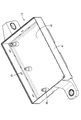
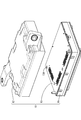
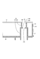
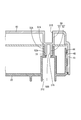
- FIG. 2 is a cross-sectional view showing a first case and a second case that are screwed together, and is a cross-sectional view taken along line VIII-VIII in FIG. Sectional drawing showing the 1st case and 2nd case in a comparative example
- the electrical device 10 shown in FIGS. 1, 4 and 5 is, for example, an ECU (Electronic Control Unit), and supplies power to various in-vehicle electrical components from a power source such as a battery and controls supply power. Is what you do.
- ECU Electronic Control Unit
- the electrical device 10 includes a plate-like circuit board 13, a first case 11 on which the circuit board 13 is disposed, and a second case attached to the first case 11 so as to cover the circuit board 13. 12.
- a plurality of connectors 15 are arranged in the first case 11.
- the circuit board 13 has a substantially rectangular shape as shown in FIG. A conductive pattern (not shown) is formed on the front surface and / or back surface of the circuit board 13 by a printed wiring technique.
- the circuit board 13 is provided with a plurality of board holes 13A (through holes) used when the circuit board 13 is fixed to the first case 11 and the second case 12.
- the first case 11 has a substantially box shape, and includes a substantially rectangular first bottom plate portion 20 and a first side wall portion 21 that rises from its four sides. ing.
- a plurality of first claw portions 23 that are used when temporarily assembled with the second case 12 are provided on the outer side surface of the first side wall portion 21.
- a plurality of first tube portions 30 are formed so as to protrude from the first bottom plate portion 20. In the present embodiment, four first cylindrical portions 30 are provided in the vicinity of the two first side wall portions 21 in the vicinity where the connector 15 is disposed.
- the second case 12 has a substantially box shape similar to the first case 11, and is formed by rising from a substantially rectangular second bottom plate portion 40 and its four sides. And a side wall 41.
- a second claw portion 43 that is engaged with the first claw portion 23 of the first case 11 is provided on the inner side surface of the second side wall portion.
- the same number of second claw portions 43 as the first claw portions 23 are provided.
- a plurality of second cylindrical portions 50 are formed so as to protrude from the second bottom plate portion 40.
- the same number of second cylinders 50 as the first cylinders 30 are provided at positions corresponding to the first cylinders 30.
- the configuration of the first cylindrical portion 30 in the first case 11 will be described.
- the first cylindrical portion 30 has a hollow cylindrical shape, and is connected to the first large diameter portion 31 and the first large diameter portion 31 arranged on the base end side in the vicinity of the first bottom plate portion 20. It has the 1st small diameter part 32 (outer cylinder part) distribute
- the first large diameter portion 31 is larger in diameter than the first small diameter portion 32.
- the first large diameter portion 31 is opened in the first bottom plate portion 20 and has a first bottom plate hole 31C.
- one end portion of the first small diameter portion 32 protrudes inward from the inner peripheral surface of the first cylindrical portion 30 and is a fixed portion.
- 33 (contacted portion) is provided, and the fixing portion 33 is provided over the entire circumference in the first large diameter portion 31 and the first small diameter portion 32.
- a first screw insertion hole 31 ⁇ / b> B is formed at the inner peripheral edge of the fixing portion 33.
- the distal end side of the first small diameter portion 32 is opened, and a fitting hole 32B (fitting hole) for inserting a second small diameter portion 52 described later is provided therein.
- the tip part which is the other end part has a first substrate pressing part 32A (pressing part).
- claw part 23 provided in the 1st side wall part 21 of the 1st case 11 is demonstrated.
- the first claw portion 23 is provided on the outer surface of the four first side wall portions 21.
- the first claw portion 23 is provided at the distal end portion of the first side wall portion 21, and is formed in a tapered shape toward the distal end of the first side wall portion 21.
- the second cylindrical portion 50 has a hollow cylindrical shape, and has a second large diameter portion 51 (large diameter portion) and a second large diameter portion arranged on the proximal end side in the vicinity of the second bottom plate portion 40. 51, and a second small diameter portion 52 (inner tube portion) arranged on the distal end side of the second tube portion 50.
- the second large diameter portion 51 has a diameter larger than the external diameter of the second small diameter portion 52 and is open in the second bottom plate portion 40 and has a second bottom plate hole 51B.
- the second large diameter portion 51 is configured not to move relative to the outer peripheral surface of the second small diameter portion 52.
- the second large diameter portion 51 is integrally formed on the outer peripheral surface of the second small diameter portion 52, but the internal space of the second large diameter portion 51 and the internal space of the second small diameter portion 52 are Not communicating.
- the step portion is the second substrate pressing portion 51A.
- the second small diameter portion 52 is open at the tip and has a screwing hole 52B (screwing hole) into which a screw 60 having a screw thread is screwed.
- the distal end portion of the second small diameter portion 52 is a second tube portion abutting portion 52A, and abuts against the fixing portion 33 in a state where the screw 60 is screwed into the screwing hole 52B.
- the second cylinder portion contact portion 52A contacts the surface of the fixing portion 33 on the fitting hole 32B side.
- the inner diameter dimension of the first small diameter part 32 is larger than the outer dimension of the second small diameter part 52, and the first small diameter part 32 is arranged so as to be fitted on the second small diameter part 52.
- claw part 43 provided in the 2nd side wall part 41 of the 2nd case 12 is demonstrated.
- the second claw portion 43 is provided on the inner peripheral surface of the four second side wall portions 41.
- the second claw portion 43 is provided so as to protrude inward at the center portion of the second side wall portion 41, and is inclined so as to descend toward the tip of the second side wall portion 41. Has been.
- each board hole 13 ⁇ / b> A matches each corresponding fitting hole 32 ⁇ / b> B.
- each second small diameter portion 52 is inserted into the corresponding fitting hole 32 ⁇ / b> B through the substrate hole 13 ⁇ / b> A, and the second case 12 is positioned with respect to the first case 11.
- the first side wall portion 21 and the second side wall portion 41 are arranged so as to overlap each other so that the second side wall portion 41 is arranged outside.
- the first case 11 and the second case 12 are temporarily assembled by the first claw portion 23 and the second claw portion 43.
- the second case 12 when the second case 12 is assembled to the first case 11, the second side wall portion 41 moves downward. Then, the inclined surface of the second claw part 43 moves along the inclined surface of the first claw part 23, and when the second claw part 43 gets over the first claw stepped part 24 of the first claw part 23, the second claw part 43 has a second claw part 43.
- the claw stepped portions 44 are locked with each other. In this state, in FIG. 7, the first case 11 can move only in the upward direction, the second case 12 can move only in the downward direction, and cannot move in the direction away from each other.
- the first screw insertion hole 31B matches the screwing hole 52B, and the first screw insertion hole
- the screw hole 52B and the first large diameter portion 31 communicate with each other through 31B.
- the tip of the first substrate pressing portion 32A is in contact with the circuit board 13, and specifically, is in contact with the edge of the substrate hole 13A.
- the second board pressing part 51A of the second large diameter part 51 is in contact with the circuit board 13, and specifically, in contact with the hole edge part of the board hole 13A. That is, the circuit board 13 is sandwiched between the second substrate pressing portion 51A and the first substrate pressing portion 32A of the second large diameter portion 51. In this state, there is a small gap between the fixed portion 33 and the second cylindrical portion abutting portion 52A.
- the first case 11 and the second case 12 temporarily assembled as shown in FIGS. 5 and 8 are reversed in the vertical direction.
- the first case 11 and the second case 12 are temporarily assembled and do not move in directions away from each other, the first case 11 and the second case 12 are detached during the reversing operation. There is no.
- the circuit board 13 is sandwiched between the second board pressing part 51A and the first board pressing part 32A of the second large diameter part 51, the circuit board 13 is suppressed from rattling.
- the screw 60 is inserted into the screwing hole 52B through the first screw insertion hole 31B and screwed. Then, there is no small gap between the fixing portion 33 and the second cylindrical portion abutting portion 52A, and the first case 11 and the second case 12 are firmly fixed. Further, the screw 60 engages the head 60 ⁇ / b> A to press the fixing portion 33, and the pressing force is transmitted to the first substrate pressing portion 32 ⁇ / b> A via the first small diameter portion 32. With the pressing force, the first substrate pressing portion 32A can sandwich and fix the circuit board 13 between the second substrate pressing portion 51A.
- a screw hole is provided at an end portion of the first cylinder portion 111 ⁇ / b> A that protrudes from the first bottom plate portion 140 of the first case 111, and a board hole is formed at a corresponding position of the circuit board 113. Is provided.
- the protruding end portion of the second cylindrical portion 112A provided to protrude from the second bottom plate portion 120 of the second case 112 is open and has a screw insertion hole therein.
- the circuit board 113 is sandwiched between the first board pressing part 111C of the first cylinder part 111A and the protruding end part of the second cylinder part 112A, and the screw 60 is screwed in that state.
- the screw 60 is inserted through the screw hole and the substrate hole while being screwed into the screw insertion hole in the second cylindrical portion 112A, the pressing force from the head of the screw 60 is applied to the first substrate pressing portion 111C.
- the circuit board 113 is sandwiched and fixed between the first board pressing part 111C and the protruding end part of the second cylinder part 112A by the pressing force.
- the contact portion A1 between the first case 111 and the circuit board 113 is subjected to a pressing force from the first case 111 due to screwing, and a distortion or the like is generated. Therefore, a conductive pattern may be formed. Can not.
- the contact portion A1 on the circuit board 113 extends over a wide range around the hole edge of the board hole, and wiring cannot be performed in the range of the diameter A2 on the circuit board 113. The area becomes narrow. As described above, in the comparative example, since the screwing position and the fixing position of the circuit board 113 are close to each other, the contact portion A1 between the first case 111 and the circuit board 113 becomes large.
- the first and second diameter small portions 32 and 52 are arranged so that a pressing force applied by screwing of the screw 60 is applied.
- the position and the fixed position of the circuit board where the first board pressing part 32A of the first small diameter part 32 is in contact with the board can be separated.
- the contact portion B1 of the circuit board 13 is within a narrow range around the hole edge of the board hole 13A, and the range where wiring cannot be performed is limited to a range with a small diameter B2.
- the circuit board 13 can be fixed using the screw 60 having the same size as the screw used in the configuration of the comparative example, and the range in which the conductive pattern cannot be formed on the circuit board 13 can be reduced. Therefore, a wide mounting area can be secured.
- the circuit board 13 in a state where the second small diameter portion 52 is inserted into the board hole 13A of the circuit board 13, the circuit board 13 is not inserted deeper than the second large diameter portion 51.
- the head 60A of the screw 60 is fixed to the fixed portion of the first small diameter portion 32.
- the first small diameter portion 32 is pressed by the head 60 ⁇ / b> A of the screw 60.
- the circuit board 13 is sandwiched between the first substrate pressing portion 32 ⁇ / b> A of the first small diameter portion 32 and the second large diameter portion 51. Thereby, the circuit board 13 can be fixed.
- the circuit board 13 is sandwiched between the second large diameter portion 51 and the first substrate pressing portion 32A, by changing the dimensions of the second large diameter portion 51 and the first substrate pressing portion 32A, The area of the area where pressure is applied to the circuit board 13 can be reduced. As a result, the area of the circuit board 13 where the conductive pattern cannot be formed can be reduced, so that the wiring density of the circuit board 13 can be improved.
- the second large diameter portion 51 is formed integrally with the outer peripheral surface of the second small diameter portion 52. Therefore, compared with the case where the 2nd diameter large part 51 and the 2nd diameter small part 52 are comprised by another component, a number of parts can be reduced.
- the electrical device 10 includes the first case 11 having the first bottom plate portion 20 having the first small diameter portion 32 and the second bottom plate portion 40 having the second small diameter portion 52.
- the first case 11 and the second case 12 are integrally assembled by screwing the shaft portion 60B of the screw 60 into the screwing hole 52B of the second small diameter portion 52. It is like that. Thereby, the wiring density of the circuit board 13 with which the electric equipment 10 is provided can be improved.
- the first claw portion 23 is formed on the first side wall portion 21 rising from the side edge of the first bottom plate portion 20, and the second side wall rising from the side edge of the second bottom plate portion 40.
- the part 41 is provided with a second claw part 43 that engages with the first claw part 23 at a position corresponding to the first claw part 23.
- the first board pressing part 32A is in contact with the circuit board 13 in a state where the first claw part 23 and the second claw part 43 are engaged.
- the circuit board 13 is made to have the first diameter by the first board pressing part 32A in a state where the first claw part 23 of the first case 11 and the second claw part 43 of the second case 12 are engaged.
- the large portion 31 (fixed portion 33) is pressed. Thereby, it is possible to prevent the circuit board 13 from rattling in a state where the first case 11 and the second case 12 are temporarily assembled.
- the electric device 10 is an ECU, the electric device 10 is not limited to this, and may be an electric junction box that switches electric power supplied from a power source to vehicle-mounted electrical components, and may be any electric device. it can.
- one circuit board 13 is accommodated in one electric device 10, but the present invention is not limited to this, and a plurality of circuit boards 13 are accommodated in one electric device 10. It is good.
- the electric device 10 includes the first claw portion 23 and the second claw portion 43, but the first claw portion 23 and the second claw portion 43 may be omitted.
Landscapes
- Engineering & Computer Science (AREA)
- Microelectronics & Electronic Packaging (AREA)
- Mounting Of Printed Circuit Boards And The Like (AREA)
Abstract
回路基板固定構造1は、ネジ(60)が螺合されている螺合孔(52B)を有する第2径小部(52)と、第2径小部(52)の外形寸法よりも大きな内径寸法を有して第2径小部(52)に外嵌する嵌合孔(32B)を有する第1径小部(32)と、第2径小部(52)の外周面に対して相対的に移動しないようになっており、且つ、第2径小部(52)の外形寸法よりも径大な第2径大部(51)とを備えており、第1径小部(32)は一方の端部には、ネジ(60)が第2径小部(52)の螺合孔(52B)に螺合された状態で、ネジ(60)の頭部(60A)が当接する固定部(33)を備え、第1径小部(32)の他方の端部には第1基板押圧部(32A)を有する。回路基板(13)は 第2径小部(52)の外形寸法よりも大きく、且つ、第2径大部(51)の外形寸法よりも小さな内径寸法を有する基板孔(13A)を有し、第2径小部(52)が基板孔(13A)に貫通した状態で、第1径小部(32)の第1基板押圧部(32A)と第2径大部(51)との間に挟持されている。
Description
本明細書に開示された技術は、回路基板固定構造、及び電気機器に関する。
電気接続箱において本体ケースとロアケースとの間に基板が配されており、基板は本体ケースかロアケースのいずれかに固定されている。この基板の固定構造の一例が特許文献1に開示されている。
特許文献1において、ケース本体に固定用ボスが立設されており、補強板とフレキシブル基板とスペーサとに対してそれぞれに設けられているねじ用孔にねじを補強板側から挿入し、固定用ボスの固定用孔にねじ止めすることにより、補強板とフレキシブル基板とスペーサとをケース本体に固定している。
しかしながら、このような基板の固定構造によると、ねじ座面が補強板を押圧し、補強板に重ねられているフレキシブル基板にその押圧力がそのまま付加される。そのため、フレキシブル基板のねじが挿入されている固定用孔の周囲部分において、ねじ座面に対応する部分とその周囲にわたって押圧力を受けて、ひずみやよれ等が生じてしまう恐れがある。フレキシブル基板においてこのようにひずみやよれ等が生じてしまう部分には、回路配線を行うことができないため、実装面積が小さくなってしまう。
本明細書に開示された技術は上記のような事情に基づいて完成されたものであって、回路基板における実装面積を小さくすることなく、回路基板の配線密度を向上させることができる、回路基板の固定構造、及びこれを用いた電気機器を提供することを目的とする。
本明細書に開示された技術に係る基板固定構造は、ネジ山を備えた軸部の一の端部に軸部よりも径大な頭部を有するネジと、ネジの軸部が螺合された螺合孔を有する内筒部と、内筒部の外形寸法よりも大きな内径寸法を有して内筒部に外嵌する嵌合孔を有する外筒部であって、外筒部の一方の端部には、ネジの軸部が内筒部の螺合孔に螺合された状態で、ネジの頭部が当接する被当接部を備え、外筒部の他方の端部には押圧部を有する外筒部と、内筒部の外周面に対して相対的に移動しないようになっており、且つ、内筒部の外形寸法よりも径大な径大部と、内筒部の外形寸法よりも大きく、且つ、径大部の外形寸法よりも小さな内径寸法を有する貫通孔を有し、内筒部が貫通孔に貫通した状態で、外筒部の押圧部と、径大部との間に挟持される回路基板とを備えている。
上記の構成によれば下記の作用効果を得ることができる。回路基板の挿通孔に内筒部を挿通させた状態では、回路基板は径大部よりも奥方には挿通されないようになっている。この内筒部に外筒部を外嵌し、ネジの軸部を内筒部の螺合孔に螺合させると、ネジの頭部が外筒部の被当接部に当接し、これにより、外筒部がネジの頭部により押圧される。すると、外筒部の押圧部と、径大部とによって、回路基板が挟持される。これにより、回路基板を固定することができる。
このとき、回路基板は、径大部と押圧部との間に挟持されるので、径大部と押圧部の寸法を変更することにより、回路基板に圧力が加えられる領域の面積を、小さくすることができる。この結果、回路基板のうち導電パターンを形成することのできない領域を小さくすることができるので、回路基板の配線密度を向上させることができる。
上記の構成に加えて、径大部は内筒部の外周面に一体に形成されていてもよい。このような構成によれば、径大部と、内筒部とを別部品で構成する場合に比べて、部品点数を減少させることができる。
本明細書に開示された技術の実施態様としては以下の態様が好ましい。
径大部は内筒部の外周面に一体に形成されていることが好ましい。
上記の構成によれば、径大部と内筒部とを別部品で構成する場合に比べて、部品点数を削減することができる。
また、本明細書に開示された電気機器は、上記の回路基板固定構造と、外筒部を備えた第1底板部を有する第1ケースと、内筒部を備えた第2底板部を有する第2ケースと、を備え、ネジの軸部を内筒部の螺合孔に螺合することにより第1ケースと前記第2ケースとが一体に組み付けられるようになっている電気機器。
上記の構成によれば、電気機器が備える回路基板の配線密度を向上させることができる。
本明細書に開示された技術の実施態様としては以下の態様が好ましい。
第1底板部の側縁から立ち上がる第1側壁部には第1爪部が形成されており、第2底板部の側縁から立ち上がる第2側壁部には、第1爪部に対応する位置に、第1爪部と係合する第2爪部が設けられていることが好ましい。
上記の構成によれば、第1ケースの第1爪部と、第2ケースの第2爪部とを係合させることにより、ネジ止めに先立って、第1ケースと第2ケースとを仮組みすることができる。
第1爪部と前記第2爪部とが係合した状態で、外筒部の押圧部は回路基板に当接していることが好ましい。
上記の構成によれば、第1ケースの第1爪部と、第2ケースの第2爪部とを係合させた状態で、回路基板は、外筒部の押圧部によって、径大部側に押圧されるようになっている。これにより、第1ケースと第2ケースとを仮組みした状態で、回路基板ががたつくことを抑制することができる。
本発明によれば、回路基板における実装面積を小さくすることなく、簡単な構成で回路基板の固定構造を実現することができ、回路基板の配線密度を向上させることができる。
本明細に開示された技術の一実施形態を図1ないし図8を参照して説明する。本実施形態において図1、4及び5に示す電気機器10は、例えばECU(Electronic Control Unit)であって、バッテリー等の電源から、各種車載電装品への電力の供給及び供給電力の制御等を行うものである。
電気機器10は、図4に示すように、板状の回路基板13と、回路基板13が配される第1ケース11と、回路基板13を覆うように第1ケース11に取り付けられる第2ケース12と、を備える。第1ケース11には複数のコネクタ15が配されている。
回路基板13は、図4に示すように、略長方形状をなす。回路基板13の表面及び裏面の双方又は一方にはプリント配線技術により図示しない導電パターンが形成されている。また、回路基板13には、回路基板13を第1ケース11第2ケース12に固定する際に用いられる基板孔13A(貫通孔)が複数設けられている。
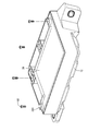
第1ケース11は、図2に示すように、略箱型形状をなしており、略長方形の第1底板部20とその4辺から立ち上がって形成されている第1側壁部21とを有している。第1側壁部21の外側面には、第2ケース12と仮組みする際に用いられる複数の第1爪部23が設けられている。また、第1底板部20からは複数の第1筒部30が突出して形成されている。本実施例においては、コネクタ15が配されている付近の2つの第1側壁部21の近傍に4つの第1筒部30が設けられている。
第2ケース12は、図3に示すように、第1ケース11と同様な略箱型形状をなしており、略長方形の第2底板部40とその4辺から立ち上がって形成されている第2側壁部41とを有している。第2側壁部の内側面には、第1ケース11の第1爪部23と係合される第2爪部43が設けられている。第2爪部43は第1爪部23と同数個設けられている。また、第2底板部40からは複数の第2筒部50が突出して形成されている。第1筒部30と同数の第2筒部50が、第1筒部30に対応した位置に設けられている。
次に、図6ないし図8を参照して、回路基板固定構造1の構成について詳細に説明する。
第1ケース11における第1筒部30の構成について説明する。第1筒部30は、内部は空洞の円筒形であり、第1底板部20近傍の基端部側において配されている第1径大部31と、第1径大部31から連なって第1筒部30の先端側に配されている第1径小部32(外筒部)とを有する。第1径大部31は第1径小部32よりも径寸法が大きい。第1径大部31は第1底板部20において開口しており第1底板孔31Cを有する。
第1径大部31と第1径小部32との連結部分において、第1径小部32の一方の端部には第1筒部30の内周面から内側に向かって突出して固定部33(被当接部)が設けられており、固定部33は第1径大部31、第1径小部32内の全周にわたって設けられている。固定部33の内周縁において第1ネジ挿入孔31Bが形成されている。
第1径小部32の先端側は開口しており、内部に後述する第2径小部52を挿入する嵌合孔32B(嵌合孔)が設けられており、第1径小部32の他方の端部である先端部には第1基板押圧部32A(押圧部)を有している。
第1ケース11の第1側壁部21に設けられている第1爪部23について説明する。図2に示すように本実施例において、第1爪部23は4つの第1側壁部21の外側面に設けられている。第1爪部23は、図6に示すように、第1側壁部21の先端部に設けられており、第1側壁部21の先端に向かってテーパ状に形成されている。
第2ケース12における第2筒部50の構成について説明する。第2筒部50は、内部は空洞の円筒形であり、第2底板部40近傍の基端部側において配されている第2径大部51(径大部)と、第2径大部51から連なって第2筒部50の先端側に配されている第2径小部52(内筒部)とを有する。第2径大部51は第2径小部52の外形寸法よりも径寸法が大きく、第2底板部40において開口しており第2底板孔51Bを有する。また、第2径大部51は第2径小部52の外周面に対して相対的に移動しないように構成されている。本実施例において、第2径大部51は第2径小部52の外周面に一体に形成されているが、第2径大部51の内部空間と第2径小部52の内部空間は連通していない。
第2径大部51と第2径小部52との連結部分の外周面において、第2径大部51は第2径小部52よりも外側に突出して段差部を形成しており、その段差部は第2基板押圧部51Aである。第2径小部52は、先端部が開口しており、内部にネジ山を有するネジ60が螺合される螺合孔52B(螺合孔)を有している。第2径小部52の先端部は第2筒部当接部52Aであり、ネジ60が螺合孔52Bに螺合された状態で、固定部33に当接する。具体的には、ネジ60が螺合孔52Bに螺合された状態で、第2筒部当接部52Aは固定部33の嵌合孔32B側の面に当接する。
第1径小部32の内径寸法は第2径小部52の外形寸法よりも大きく、第1径小部32は第2径小部52に外嵌するように配されている。
第2ケース12の第2側壁部41に設けられている第2爪部43について説明する。図3に示すように本実施例において、第2爪部43は4つの第2側壁部41の内周面に設けられている。第2爪部43は、図7に示すように、第2側壁部41の中央部において内側に突出して設けられており、第2側壁部41の先端に向かって下降するように傾斜して形成されている。
次に、図4ないし図8を参照して、回路基板13と、第1ケース11と、第2ケース12とを組み付ける工程における基板固定構造を説明する。
まず、図4及び図6に示すように、各基板孔13Aが対応する各嵌合孔32Bに合致するように回路基板13を第1ケース11上に載置する。その後、図7に示すように、各第2径小部52を基板孔13Aを介して対応する嵌合孔32Bに挿入して、第2ケース12を第1ケース11に対して位置決めする。
図7に示されるように、第1側壁部21と第2側壁部41は第2側壁部41が外側に配されるように重ね合うように配されている。このとき、第1ケース11と第2ケース12とは、第1爪部23と第2爪部43とにより仮組みされている。
詳細には、第1ケース11に第2ケース12が組み付けられる際、第2側壁部41が下方に移動する。すると、第2爪部43はその傾斜面が第1爪部23の傾斜面に沿って移動し、第1爪部23の第1爪段差部24を乗り越えると、第2爪部43の第2爪段差部44とが互いに係止される。この状態では、図7において、第1ケース11は上方向にのみ移動可能であり、第2ケース12は下方向にのみ移動可能であり、互いに外れる方向には移動不可能となっている。
このように、第1ケース11と第2ケース12とが仮組みされると、図7に示されるように、第1ネジ挿入孔31Bは螺合孔52Bに合致して、第1ネジ挿入孔31Bを介して螺合孔52Bと第1径大部31とは連通している。第1基板押圧部32Aの先端部は回路基板13に当接しており、具体的には、基板孔13Aの孔縁部に当接している。第2径大部51の第2基板押圧部51Aは回路基板13に当接しており、具体的には、基板孔13Aの孔縁部に当接している。つまり、第2径大部51の第2基板押圧部51Aと第1基板押圧部32Aとにより、回路基板13を挟んでいる。この状態では、固定部33と第2筒部当接部52Aとの間には小さな隙間が空いている状態である。
その後、ネジ止めを行うために、図5及び図8に示すように仮組みされている第1ケース11と第2ケース12を上下方向について反転させる。ここで、第1ケース11と第2ケース12とは仮組みされていて、互いに外れる方向には動くことはないので、反転動作中に第1ケース11と第2ケース12とが外れてしまうことはない。さらに、第2径大部51の第2基板押圧部51Aと第1基板押圧部32Aとにより、回路基板13を挟んでいるので、回路基板13ががたつくことが抑制される。
図8に示す反転した状態で、ネジ60を第1ネジ挿入孔31Bを介して螺合孔52B内に挿入して螺合する。すると、固定部33と第2筒部当接部52Aとの間の小さな隙間はなくなり、第1ケース11と第2ケース12とは強固に固定される。また、このネジ60の螺合によって、頭部60Aが固定部33を押圧し、その押圧力は第1径小部32を介して第1基板押圧部32Aに伝わる。その押圧力によって、第1基板押圧部32Aは第2基板押圧部51Aとの間で回路基板13を挟みこんで固定することができる。
ここで、図9を参照して、本実施例における第1径小部32及び第2径小部52を有しない基板固定構造を比較例として説明する。
比較例においては、第1ケース111の第1底板部140から突出して設けられている第1筒部111Aの端部にはネジ孔が設けられており、回路基板113の対応する位置に基板孔が設けられている。第2ケース112の第2底板部120から突出して設けられている第2筒部112Aの突出端部は開口しており、その内部にネジ挿入孔を有している。
比較例において、第1筒部111Aの第1基板押圧部111Cと第2筒部112Aの突出端部との間で回路基板113を挟んでおり、その状態でネジ60が螺合される。ネジ孔と基板孔を介してネジ60が第2筒部112A内のネジ挿入孔に螺合されつつ挿入されると、ネジ60の頭部からの押圧力が第1基板押圧部111Cに付加され、その押圧力によって第1基板押圧部111Cと第2筒部112Aの突出端部との間で回路基板113を挟みこんで固定している。
比較例において、第1ケース111と回路基板113との当接部A1には、ネジ止めによって第1ケース111からの押圧力が加わりひずみ等が発生してしまうため、導電パターンを形成することができない。比較例においては、回路基板113における当接部A1は、基板孔の孔縁の周囲において広い範囲にわたっており、回路基板113において直径A2の範囲において配線を行うことができず、回路基板113における実装面積が狭くなってしまう。このように比較例においては、ネジ止め位置と回路基板113の固定位置が接近しているため、第1ケース111と回路基板113との当接部A1は大きくなってしまう。
一方、本実施例においては、図8に示すように、第1径小部32と第2径小部52とを配することにより、ネジ60の螺合により付加される押圧力がかかるネジ止め位置と、第1径小部32の第1基板押圧部32Aが基板に当接している回路基板の固定位置を離すことができる。そのため、回路基板13における当接部B1は、基板孔13Aの孔縁の周囲において狭い範囲におさまっており、配線を行うことができない範囲は直径B2の小さい範囲におさまっている。
本実施例においては、比較例の構成において用いられるネジと同じサイズのネジ60を使って回路基板13を固定することができるとともに、回路基板13において導電パターンを形成できない範囲を小さくすることができるため、実装面積を広く確保することができる。
本実施例によると、回路基板13の基板孔13Aに第2径小部52を挿通させた状態では、回路基板13は第2径大部51よりも奥方には挿通されないようになっている。第1径小部32を外嵌し、ネジ60の軸部60Bを第2径小部52の螺合孔52Bに螺号させると、ネジ60の頭部60Aが第1径小部32の固定部33に当接し、これにより、第1径小部32がネジ60の頭部60Aにより押圧される。すると、第1径小部32の第1基板押圧部32Aと第2径大部51によって回路基板13が挟持される。これにより、回路基板13を固定することができる。
このとき、回路基板13は第2径大部51と第1基板押圧部32Aとの間に挟持されるので、第2径大部51と第1基板押圧部32Aの寸法を変更することにより、回路基板13に圧力が加えられる領域の面積を小さくすることができる。この結果、回路基板13のうち導電パターンを形成することができない領域を小さくすることができるので、回路基板13の配線密度を向上させることができる。
また、本実施形態においては、第2径大部51は第2径小部52の外周面に一体に形成されている。これにより、第2径大部51と第2径小部52とを別部品で構成する場合に比べて、部品点数を削減することができる。
また、本実施形態によれば、電気機器10は、第1径小部32を備えた第1底板部20を有する第1ケース11と、第2径小部52を備えた第2底板部40を有する第2ケース12と、を備え、ネジ60の軸部60Bを第2径小部52の螺合孔52Bに螺合することにより第1ケース11と第2ケース12とが一体に組み付けられるようになっている。これにより、電気機器10が備える回路基板13の配線密度を向上させることができる。
また、本実施形態によれば、第1底板部20の側縁から立ち上がる第1側壁部21には第1爪部23が形成されており、第2底板部40の側縁から立ち上がる第2側壁部41には、第1爪部23に対応する位置に、第1爪部23と係合する第2爪部43が設けられている。これにより、第1ケース11の第1爪部23と、第2ケース12の第2爪部43とを係合させることにより、ネジ止めに先立って、第1ケース11と第2ケース12とを仮組みすることができる。
また、本実施形態によれば、第1爪部23と第2爪部43とが係合した状態で、第1基板押圧部32Aは回路基板13に当接している。これにより、第1ケース11の第1爪部23と、第2ケース12の第2爪部43とを係合させた状態で、回路基板13は、第1基板押圧部32Aによって、第1径大部31(固定部33)側に押圧されるようになっている。これにより、第1ケース11と第2ケース12とを仮組みした状態で、回路基板13ががたつくことを抑制することができる。
<他の実施形態>
本明細書に開示された技術は上記記述及び図面によって説明した実施形態に限定されるものではなく、例えば次のような実施形態も本明細書に開示された技術の範囲に含まれる。
本明細書に開示された技術は上記記述及び図面によって説明した実施形態に限定されるものではなく、例えば次のような実施形態も本明細書に開示された技術の範囲に含まれる。
(1)本実施形態に係る電気機器10はECUとしたが、これに限られず、電源から車載電装品に供給される電力をスイッチングする電気接続箱としてもよく、任意の電気機器とすることができる。
(2)本実施形態においては、1つの電気機器10に1つの回路基板13が収容される構成としたが、これに限られず、1つの電気機器10に複数の回路基板13が収容される構成としてもよい。
(3)本実施形態においては、第1爪部23と第2爪部43とが係合した状態で、固定部33と第2筒部当接部52Aとの間には小さな隙間が空いている状態としたが、これに限られず、第1爪部23と第2爪部43とが係合した状態で、固定部33と第2筒部当接部52Aとが当接していてもよい。
(4)本実施形態においては、電気機器10は、第1爪部23と第2爪部43を備える構成としたが、第1爪部23と第2爪部43は省略してもよい。
10:電気機器
11:第1ケース
12:第2ケース
13:回路基板
13A:基板孔(貫通孔)
20:第1底板部
21:第1側壁部
23:第1爪部
30:第1筒部
31:第1径大部
32:第1径小部(外筒部)
32A:第1基板押圧部(押圧部)
32B:嵌合孔
33:固定部(被当接部)
40:第2底板部
41:第2側壁部
43:第2爪部
50:第2筒部
51:第2径大部(径大部)
51A:第2基板押圧部
52:第2径小部(内筒部)
52A:螺合孔
60:ネジ
60A:頭部
60B:軸部
11:第1ケース
12:第2ケース
13:回路基板
13A:基板孔(貫通孔)
20:第1底板部
21:第1側壁部
23:第1爪部
30:第1筒部
31:第1径大部
32:第1径小部(外筒部)
32A:第1基板押圧部(押圧部)
32B:嵌合孔
33:固定部(被当接部)
40:第2底板部
41:第2側壁部
43:第2爪部
50:第2筒部
51:第2径大部(径大部)
51A:第2基板押圧部
52:第2径小部(内筒部)
52A:螺合孔
60:ネジ
60A:頭部
60B:軸部
Claims (5)
- ネジ山を備えた軸部の一の端部に、前記軸部よりも径大な頭部を有するネジと、
前記ネジの前記軸部が螺合された螺合孔を有する内筒部と、
前記内筒部の外形寸法よりも大きな内径寸法を有して前記内筒部に外嵌する嵌合孔を有する外筒部であって、前記外筒部の一方の端部には、前記ネジの前記軸部が前記内筒部の前記螺合孔に螺合された状態で、前記ネジの前記頭部が当接する被当接部を備え、前記外筒部の他方の端部には押圧部を有する前記外筒部と、
前記内筒部の外周面に対して相対的に移動しないようになっており、且つ、前記内筒部の外形寸法よりも径大な径大部と、
前記内筒部の外形寸法よりも大きく、且つ、前記径大部の外形寸法よりも小さな内径寸法を有する貫通孔を有し、前記内筒部が前記貫通孔に貫通した状態で、前記外筒部の前記押圧部と、前記径大部との間に挟持される回路基板と、
を備えた回路基板固定構造。 - 前記径大部は前記内筒部の外周面に一体に形成されている、請求項1に記載の回路基板固定構造。
- 請求項1または請求項2に記載の回路基板固定構造を備えた電気機器であって、
前記外筒部を備えた第1底板部を有する第1ケースと、
前記内筒部を備えた第2底板部を有する第2ケースと、を備え、
前記ネジの前記軸部を前記内筒部の前記螺合孔に螺合することにより前記第1ケースと前記第2ケースとが一体に組み付けられるようになっている電気機器。 - 前記第1底板部の側縁から立ち上がる第1側壁部には第1爪部が形成されており、
前記第2底板部の側縁から立ち上がる第2側壁部には、前記第1爪部に対応する位置に、前記第1爪部と係合する第2爪部が設けられている、請求項3に記載の電気機器。 - 前記第1爪部と前記第2爪部とが係合した状態で、
前記前記外筒部の前記押圧部は前記回路基板に当接している、請求項4に記載の電気機器。
Priority Applications (2)
| Application Number | Priority Date | Filing Date | Title |
|---|---|---|---|
| US16/318,341 US20190239378A1 (en) | 2016-07-29 | 2017-07-18 | Circuit board fixation structure and electrical apparatus |
| CN201780046041.6A CN109479383A (zh) | 2016-07-29 | 2017-07-18 | 电路基板固定构造及电气设备 |
Applications Claiming Priority (2)
| Application Number | Priority Date | Filing Date | Title |
|---|---|---|---|
| JP2016-149901 | 2016-07-29 | ||
| JP2016149901A JP6627683B2 (ja) | 2016-07-29 | 2016-07-29 | 電気機器 |
Publications (1)
| Publication Number | Publication Date |
|---|---|
| WO2018021085A1 true WO2018021085A1 (ja) | 2018-02-01 |
Family
ID=61016786
Family Applications (1)
| Application Number | Title | Priority Date | Filing Date |
|---|---|---|---|
| PCT/JP2017/025876 Ceased WO2018021085A1 (ja) | 2016-07-29 | 2017-07-18 | 回路基板固定構造、及び電気機器 |
Country Status (4)
| Country | Link |
|---|---|
| US (1) | US20190239378A1 (ja) |
| JP (1) | JP6627683B2 (ja) |
| CN (1) | CN109479383A (ja) |
| WO (1) | WO2018021085A1 (ja) |
Cited By (2)
| Publication number | Priority date | Publication date | Assignee | Title |
|---|---|---|---|---|
| EP3675298A1 (en) * | 2018-12-28 | 2020-07-01 | Yazaki Corporation | Electrical connection box |
| CN118564539A (zh) * | 2024-08-01 | 2024-08-30 | 遂宁鑫峰科技有限公司 | 一种电路板钻孔定位用组合铆钉 |
Families Citing this family (5)
| Publication number | Priority date | Publication date | Assignee | Title |
|---|---|---|---|---|
| JP7164966B2 (ja) * | 2018-04-09 | 2022-11-02 | 株式会社デンソーテン | 電子機器 |
| CN112449538A (zh) * | 2019-08-28 | 2021-03-05 | 高准有限公司 | 用于电子产品的灌封工艺的电路板支撑组件和电子产品 |
| CN111010837B (zh) * | 2019-12-10 | 2021-01-15 | 珠海横琴新区辉腾电子科技有限公司 | 一种节能嵌入式控制系统 |
| CN115988802A (zh) * | 2022-12-30 | 2023-04-18 | 重庆联纵智能科技有限公司 | 基于电磁感应技术的数据传输装置 |
| CN116887539A (zh) * | 2023-07-27 | 2023-10-13 | 广东美的制冷设备有限公司 | 一种智能终端 |
Citations (4)
| Publication number | Priority date | Publication date | Assignee | Title |
|---|---|---|---|---|
| JPS5866684U (ja) * | 1981-10-29 | 1983-05-06 | 株式会社東芝 | 筐体接合案内装置 |
| JPH0638291U (ja) * | 1992-10-22 | 1994-05-20 | 小島プレス工業株式会社 | コントロールボックスの組立構造 |
| JPH0786770A (ja) * | 1993-09-13 | 1995-03-31 | Fujitsu Ltd | プラスチックケースへの部品の収容固定構造 |
| JPH09321463A (ja) * | 1996-05-24 | 1997-12-12 | Kokusai Electric Co Ltd | 電子機器の筐体構造 |
Family Cites Families (11)
| Publication number | Priority date | Publication date | Assignee | Title |
|---|---|---|---|---|
| JPH0715711B2 (ja) * | 1988-11-18 | 1995-02-22 | 株式会社田村電機製作所 | プリペイドカード処理装置 |
| JPH02137084U (ja) * | 1989-04-14 | 1990-11-15 | ||
| JP2933845B2 (ja) * | 1995-02-17 | 1999-08-16 | 三菱電機株式会社 | 印刷回路基板取付装置 |
| JP3576085B2 (ja) * | 2000-09-13 | 2004-10-13 | 株式会社東芝 | 電子機器 |
| US7643273B2 (en) * | 2006-11-08 | 2010-01-05 | Super Micro Computer, Inc. | Control device of connection studs of a computer |
| US7333347B1 (en) * | 2006-12-18 | 2008-02-19 | Ablecom Computer Inc. | Screwing control device of a computer chassis |
| JP4544337B2 (ja) * | 2008-04-25 | 2010-09-15 | 日亜化学工業株式会社 | 表示装置 |
| CN102955522A (zh) * | 2011-08-19 | 2013-03-06 | 鸿富锦精密工业(深圳)有限公司 | 主板固定装置 |
| IN2013MU01206A (ja) * | 2013-03-28 | 2015-04-10 | Control Tech Ltd | |
| JP2015018936A (ja) * | 2013-07-11 | 2015-01-29 | パナソニックIpマネジメント株式会社 | 電子機器と、それを搭載した自動車 |
| JP6332118B2 (ja) * | 2015-04-10 | 2018-05-30 | 株式会社デンソー | 電子装置 |
-
2016
- 2016-07-29 JP JP2016149901A patent/JP6627683B2/ja active Active
-
2017
- 2017-07-18 US US16/318,341 patent/US20190239378A1/en not_active Abandoned
- 2017-07-18 WO PCT/JP2017/025876 patent/WO2018021085A1/ja not_active Ceased
- 2017-07-18 CN CN201780046041.6A patent/CN109479383A/zh active Pending
Patent Citations (4)
| Publication number | Priority date | Publication date | Assignee | Title |
|---|---|---|---|---|
| JPS5866684U (ja) * | 1981-10-29 | 1983-05-06 | 株式会社東芝 | 筐体接合案内装置 |
| JPH0638291U (ja) * | 1992-10-22 | 1994-05-20 | 小島プレス工業株式会社 | コントロールボックスの組立構造 |
| JPH0786770A (ja) * | 1993-09-13 | 1995-03-31 | Fujitsu Ltd | プラスチックケースへの部品の収容固定構造 |
| JPH09321463A (ja) * | 1996-05-24 | 1997-12-12 | Kokusai Electric Co Ltd | 電子機器の筐体構造 |
Cited By (5)
| Publication number | Priority date | Publication date | Assignee | Title |
|---|---|---|---|---|
| EP3675298A1 (en) * | 2018-12-28 | 2020-07-01 | Yazaki Corporation | Electrical connection box |
| CN111384696A (zh) * | 2018-12-28 | 2020-07-07 | 矢崎总业株式会社 | 电连接盒 |
| US10819048B2 (en) | 2018-12-28 | 2020-10-27 | Yazaki Corporation | Electrical connection box |
| CN111384696B (zh) * | 2018-12-28 | 2021-09-10 | 矢崎总业株式会社 | 电连接盒 |
| CN118564539A (zh) * | 2024-08-01 | 2024-08-30 | 遂宁鑫峰科技有限公司 | 一种电路板钻孔定位用组合铆钉 |
Also Published As
| Publication number | Publication date |
|---|---|
| JP2018019012A (ja) | 2018-02-01 |
| CN109479383A (zh) | 2019-03-15 |
| US20190239378A1 (en) | 2019-08-01 |
| JP6627683B2 (ja) | 2020-01-08 |
Similar Documents
| Publication | Publication Date | Title |
|---|---|---|
| WO2018021085A1 (ja) | 回路基板固定構造、及び電気機器 | |
| US10063121B2 (en) | Electric motor control apparatus | |
| JP7051297B2 (ja) | 電子機器及びロボットコントローラ | |
| JP6451569B2 (ja) | 電子装置 | |
| JP2011071342A (ja) | 基板保持装置 | |
| JP2010110059A (ja) | 電気接続箱および該電気接続箱の組立方法 | |
| JP2013084484A (ja) | コネクタ | |
| US11239583B2 (en) | Connector having fitting protrusion connected to flat cable | |
| JP2017098332A (ja) | 電子回路装置 | |
| WO2016002749A1 (ja) | 電気接続箱 | |
| JP5939918B2 (ja) | 車載カメラ装置 | |
| JP2009231472A (ja) | 電子機器 | |
| WO2014141990A1 (ja) | 基板補強構造 | |
| WO2020170793A1 (ja) | 電気接続箱 | |
| JP4880492B2 (ja) | 電子装置のハウジング構造体及びハウジング構造体の形成方法 | |
| US11398692B2 (en) | Socket with integrated flex connector | |
| US20090163049A1 (en) | Electronic module | |
| JP2016059242A (ja) | 電力変換装置 | |
| JP2013030291A (ja) | コネクタ保持構造、電子機器、電動機制御装置 | |
| JP2019016514A (ja) | コネクタの取付構造およびコネクタシールド | |
| JP2017135185A (ja) | 電子制御装置 | |
| JP2017199630A (ja) | バスバー及び電気接続箱 | |
| JP6656017B2 (ja) | 制御基板及び電気接続箱 | |
| JP2011134868A (ja) | プリント回路板取付構造 | |
| JP2022086537A (ja) | 電子機器 |
Legal Events
| Date | Code | Title | Description |
|---|---|---|---|
| 121 | Ep: the epo has been informed by wipo that ep was designated in this application |
Ref document number: 17834093 Country of ref document: EP Kind code of ref document: A1 |
|
| NENP | Non-entry into the national phase |
Ref country code: DE |
|
| 122 | Ep: pct application non-entry in european phase |
Ref document number: 17834093 Country of ref document: EP Kind code of ref document: A1 |