WO2018020643A1 - 液晶パネル及び表示装置 - Google Patents
液晶パネル及び表示装置 Download PDFInfo
- Publication number
- WO2018020643A1 WO2018020643A1 PCT/JP2016/072191 JP2016072191W WO2018020643A1 WO 2018020643 A1 WO2018020643 A1 WO 2018020643A1 JP 2016072191 W JP2016072191 W JP 2016072191W WO 2018020643 A1 WO2018020643 A1 WO 2018020643A1
- Authority
- WO
- WIPO (PCT)
- Prior art keywords
- wiring
- substrate
- liquid crystal
- crystal panel
- conductor
- Prior art date
- Legal status (The legal status is an assumption and is not a legal conclusion. Google has not performed a legal analysis and makes no representation as to the accuracy of the status listed.)
- Ceased
Links
Images





Classifications
-
- G—PHYSICS
- G02—OPTICS
- G02F—OPTICAL DEVICES OR ARRANGEMENTS FOR THE CONTROL OF LIGHT BY MODIFICATION OF THE OPTICAL PROPERTIES OF THE MEDIA OF THE ELEMENTS INVOLVED THEREIN; NON-LINEAR OPTICS; FREQUENCY-CHANGING OF LIGHT; OPTICAL LOGIC ELEMENTS; OPTICAL ANALOGUE/DIGITAL CONVERTERS
- G02F1/00—Devices or arrangements for the control of the intensity, colour, phase, polarisation or direction of light arriving from an independent light source, e.g. switching, gating or modulating; Non-linear optics
- G02F1/01—Devices or arrangements for the control of the intensity, colour, phase, polarisation or direction of light arriving from an independent light source, e.g. switching, gating or modulating; Non-linear optics for the control of the intensity, phase, polarisation or colour
- G02F1/13—Devices or arrangements for the control of the intensity, colour, phase, polarisation or direction of light arriving from an independent light source, e.g. switching, gating or modulating; Non-linear optics for the control of the intensity, phase, polarisation or colour based on liquid crystals, e.g. single liquid crystal display cells
- G02F1/133—Constructional arrangements; Operation of liquid crystal cells; Circuit arrangements
- G02F1/1333—Constructional arrangements; Manufacturing methods
- G02F1/1345—Conductors connecting electrodes to cell terminals
- G02F1/13452—Conductors connecting driver circuitry and terminals of panels
-
- G—PHYSICS
- G02—OPTICS
- G02F—OPTICAL DEVICES OR ARRANGEMENTS FOR THE CONTROL OF LIGHT BY MODIFICATION OF THE OPTICAL PROPERTIES OF THE MEDIA OF THE ELEMENTS INVOLVED THEREIN; NON-LINEAR OPTICS; FREQUENCY-CHANGING OF LIGHT; OPTICAL LOGIC ELEMENTS; OPTICAL ANALOGUE/DIGITAL CONVERTERS
- G02F1/00—Devices or arrangements for the control of the intensity, colour, phase, polarisation or direction of light arriving from an independent light source, e.g. switching, gating or modulating; Non-linear optics
- G02F1/01—Devices or arrangements for the control of the intensity, colour, phase, polarisation or direction of light arriving from an independent light source, e.g. switching, gating or modulating; Non-linear optics for the control of the intensity, phase, polarisation or colour
- G02F1/13—Devices or arrangements for the control of the intensity, colour, phase, polarisation or direction of light arriving from an independent light source, e.g. switching, gating or modulating; Non-linear optics for the control of the intensity, phase, polarisation or colour based on liquid crystals, e.g. single liquid crystal display cells
- G02F1/133—Constructional arrangements; Operation of liquid crystal cells; Circuit arrangements
- G02F1/1333—Constructional arrangements; Manufacturing methods
- G02F1/1339—Gaskets; Spacers; Sealing of cells
-
- G—PHYSICS
- G02—OPTICS
- G02F—OPTICAL DEVICES OR ARRANGEMENTS FOR THE CONTROL OF LIGHT BY MODIFICATION OF THE OPTICAL PROPERTIES OF THE MEDIA OF THE ELEMENTS INVOLVED THEREIN; NON-LINEAR OPTICS; FREQUENCY-CHANGING OF LIGHT; OPTICAL LOGIC ELEMENTS; OPTICAL ANALOGUE/DIGITAL CONVERTERS
- G02F1/00—Devices or arrangements for the control of the intensity, colour, phase, polarisation or direction of light arriving from an independent light source, e.g. switching, gating or modulating; Non-linear optics
- G02F1/01—Devices or arrangements for the control of the intensity, colour, phase, polarisation or direction of light arriving from an independent light source, e.g. switching, gating or modulating; Non-linear optics for the control of the intensity, phase, polarisation or colour
- G02F1/13—Devices or arrangements for the control of the intensity, colour, phase, polarisation or direction of light arriving from an independent light source, e.g. switching, gating or modulating; Non-linear optics for the control of the intensity, phase, polarisation or colour based on liquid crystals, e.g. single liquid crystal display cells
- G02F1/133—Constructional arrangements; Operation of liquid crystal cells; Circuit arrangements
- G02F1/1333—Constructional arrangements; Manufacturing methods
- G02F1/1343—Electrodes
- G02F1/134309—Electrodes characterised by their geometrical arrangement
-
- G—PHYSICS
- G02—OPTICS
- G02F—OPTICAL DEVICES OR ARRANGEMENTS FOR THE CONTROL OF LIGHT BY MODIFICATION OF THE OPTICAL PROPERTIES OF THE MEDIA OF THE ELEMENTS INVOLVED THEREIN; NON-LINEAR OPTICS; FREQUENCY-CHANGING OF LIGHT; OPTICAL LOGIC ELEMENTS; OPTICAL ANALOGUE/DIGITAL CONVERTERS
- G02F1/00—Devices or arrangements for the control of the intensity, colour, phase, polarisation or direction of light arriving from an independent light source, e.g. switching, gating or modulating; Non-linear optics
- G02F1/01—Devices or arrangements for the control of the intensity, colour, phase, polarisation or direction of light arriving from an independent light source, e.g. switching, gating or modulating; Non-linear optics for the control of the intensity, phase, polarisation or colour
- G02F1/13—Devices or arrangements for the control of the intensity, colour, phase, polarisation or direction of light arriving from an independent light source, e.g. switching, gating or modulating; Non-linear optics for the control of the intensity, phase, polarisation or colour based on liquid crystals, e.g. single liquid crystal display cells
- G02F1/133—Constructional arrangements; Operation of liquid crystal cells; Circuit arrangements
- G02F1/136—Liquid crystal cells structurally associated with a semi-conducting layer or substrate, e.g. cells forming part of an integrated circuit
- G02F1/1362—Active matrix addressed cells
- G02F1/1365—Active matrix addressed cells in which the switching element is a two-electrode device
-
- G—PHYSICS
- G02—OPTICS
- G02F—OPTICAL DEVICES OR ARRANGEMENTS FOR THE CONTROL OF LIGHT BY MODIFICATION OF THE OPTICAL PROPERTIES OF THE MEDIA OF THE ELEMENTS INVOLVED THEREIN; NON-LINEAR OPTICS; FREQUENCY-CHANGING OF LIGHT; OPTICAL LOGIC ELEMENTS; OPTICAL ANALOGUE/DIGITAL CONVERTERS
- G02F2201/00—Constructional arrangements not provided for in groups G02F1/00 - G02F7/00
- G02F2201/50—Protective arrangements
-
- G—PHYSICS
- G02—OPTICS
- G02F—OPTICAL DEVICES OR ARRANGEMENTS FOR THE CONTROL OF LIGHT BY MODIFICATION OF THE OPTICAL PROPERTIES OF THE MEDIA OF THE ELEMENTS INVOLVED THEREIN; NON-LINEAR OPTICS; FREQUENCY-CHANGING OF LIGHT; OPTICAL LOGIC ELEMENTS; OPTICAL ANALOGUE/DIGITAL CONVERTERS
- G02F2202/00—Materials and properties
- G02F2202/22—Antistatic materials or arrangements
Definitions
- the present invention relates to a liquid crystal panel in which liquid crystal is sealed between two substrates, and a display device including the liquid crystal panel.
- a liquid crystal display device that displays an image includes a liquid crystal panel (for example, Patent Document 1).
- a liquid crystal panel for example, Patent Document 1
- two substrates are connected to each other with a gap provided by a seal disposed along the periphery of the substrate. Liquid crystal is sealed inside the seal (region surrounded by the seal).
- a plurality of pixel electrodes are formed on one of the two substrates.
- a common electrode is formed on the other substrate.
- Each of the plurality of pixel electrodes is opposed to the common electrode.
- a voltage is applied to the pixel electrode with reference to the potential of the common electrode.
- the state of the liquid crystal molecules varies depending on the voltage applied to the pixel electrode.
- the intensity of light emitted to the outside of the liquid crystal panel via the pixel electrode is determined according to the state of the liquid crystal molecules.
- a common wiring (Vcom wiring) conducting to the common electrode is formed along the seal.
- an outer wiring (GND wiring) is further provided outside the common wiring. Therefore, for example, even when electrostatic discharge (ESD) occurs when a human body touches a liquid crystal panel, the current generated by the flow of static electricity (hereinafter referred to as electrostatic current) flows through the outer wiring and flows into the common wiring. There is no. Thereby, an electrostatic current does not flow through a circuit or a wiring arranged in the vicinity of the common wiring. As a result, it is possible to prevent the occurrence of malfunction of the circuit, disconnection of wiring, fusion of adjacent wiring, and the like.
- Static electricity is also generated during the manufacturing process of liquid crystal panels.
- a polarizing plate is attached to the plate surface of the substrate on which the common electrode is formed. For example, when a foreign substance is mixed between the polarizing plate and the substrate, or when the polarizing plate is scratched, the polarizing plate is peeled off from the substrate and a new polarizing plate is attached. When the polarizing plate is peeled off from the substrate, static electricity is generated.
- liquid crystal panel As a conventional liquid crystal panel, there is a liquid crystal panel in which a common wiring is connected to a common electrode through a seal, and a plurality of inner wirings are formed in the vicinity of the common wiring inside the seal. These inner wirings are spare wirings used to connect two wirings separated by disconnection, for example, when the wiring connected to the plurality of pixel electrodes is disconnected.
- the present invention has been made in view of such circumstances, and an object of the present invention is to provide a liquid crystal panel capable of suppressing circuit breakage due to static electricity and a display device including the liquid crystal panel.
- the two substrates are connected to each other with a gap between the two substrates via a connecting member disposed along the periphery of the substrate.
- the inner wiring formed along the connecting member inside the connecting member in one of the two substrates, and the connecting in the one substrate A conductor disposed between the member and the inner wiring in a non-contact manner with the connecting member and the inner wiring is provided.
- a display device includes the above-described liquid crystal panel and an irradiation unit that irradiates light to the liquid crystal panel, and the liquid crystal panel displays an image using light irradiated by the irradiation unit.
- a liquid crystal panel capable of suppressing circuit destruction due to static electricity and a display device including the liquid crystal panel.
- FIG. 2 is a schematic diagram of a display device in Embodiment 1.
- FIG. It is a front view of a liquid crystal panel. It is a partial front view of the liquid crystal panel from which the CF substrate and the polarizing plate were removed. It is the other partial front view of the liquid crystal panel from which the CF substrate and the polarizing plate were removed. It is explanatory drawing of spare wiring. It is another explanatory view of spare wiring. It is the elements on larger scale of substrate wiring.
- FIG. 5 is a partial front view of a liquid crystal panel in a second embodiment.
- FIG. 10 is an external view of a conductor in a third embodiment.
- FIG. 10 is an external view of a conductor in a fourth embodiment.
- FIG. 10 is a partial enlarged view of substrate wiring in a fifth embodiment.
- FIG. 10 is a partial front view of a liquid crystal panel in a sixth embodiment.
- FIG. 1 is a schematic diagram of a display device 1 according to the first embodiment.
- the display device 1 includes a liquid crystal panel 10 having a rectangular plate shape and a backlight device 11.
- FIG. 1 shows a longitudinal section of the liquid crystal panel 10.
- the backlight device 11 irradiation unit
- the liquid crystal panel 10 displays an image using light emitted from the backlight device 11.
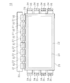
- FIG. 2 is a front view of the liquid crystal panel 10.
- the liquid crystal panel 10 includes a rectangular TFT substrate 20 on which light irradiated by the backlight device 11 is incident and a rectangular CF substrate 21 that emits light.
- the TFT substrate 20 includes a plurality of pixel electrodes 26, 26,..., A plurality of TFTs (Thin Film Transistors) 28, 28,... (See FIG. 3), and the CF substrate 21 includes a common electrode 27 ( A second electrode), a color filter (not shown), and the like.
- the light irradiated by the backlight device 11 is incident from the rear surface of the TFT substrate 20 and is emitted from the front surface of the CF substrate 21.
- Each of the TFT substrate 20 and the CF substrate 21 is transparent and is made of, for example, glass.
- the front surface of the TFT substrate 20 faces the rear surface of the CF substrate 21.
- a rectangular frame-shaped seal portion 22 (connection member) is disposed along the periphery of the TFT substrate 20 and the CF substrate 21.
- the seal portion 22 is continuous over the entire circumference of the TFT substrate 20 and the CF substrate 21.
- the TFT substrate 20 and the CF substrate 21 are connected to each other with a gap therebetween via a seal portion 22.
- the seal portion 22 is bonded to the TFT substrate 20 and the CF substrate 21. Thereby, the connection of the TFT substrate 20 and the CF substrate 21 is realized.
- a liquid crystal 23 is sealed inside the seal portion 22 (region surrounded by the seal portion 22).
- a polarizing plate 24 is attached to the rear surface of the TFT substrate 20.
- the light irradiated by the backlight device 11 passes through the polarizing plate 24 and the TFT substrate 20 in this order.
- the polarizing plate 24 transmits only the light whose electric field vibrates in a specific direction among the light irradiated by the backlight device 11.
- a polarizing plate 25 is attached to the entire front surface of the CF substrate 21.
- the light irradiated by the backlight device 11 is transmitted in the order of the polarizing plate 24, the TFT substrate 20, the liquid crystal 23, the CF substrate 21, and the polarizing plate 25.
- the polarizing plate 25 transmits only light whose electric field oscillates in a specific direction among light transmitted through the CF substrate 21.
- the specific direction related to the polarizing plate 24 may be the same direction as the specific direction related to the polarizing plate 25, or may be different from the specific direction related to the polarizing plate 25.
- FIG. 3 is a partial front view of the liquid crystal panel 10 with the CF substrate 21 and the polarizing plate 25 removed.
- FIG. 3 shows an upper left portion of the liquid crystal panel 10 as viewed from the front side. The connection between the two lines is indicated by a black circle. The intersection of two lines where no black circle is shown indicates no connection.
- a plurality of pixel electrodes 26, 26,... are formed in a lattice shape inside the seal portion 22 in the TFT substrate 20.
- the plurality of pixel electrodes 26, 26,... are transparent and arranged in the left-right direction and the up-down direction.
- Each of the plurality of pixel electrodes 26, 26,... Has a plate shape, and each of the plurality of pixel electrodes 26, 26,.
- a plate-like common electrode 27 is formed on the CF substrate 21.
- the common electrode 27 is also transparent.
- the plate surface of the common electrode 27 is opposed to the plate surfaces of all the pixel electrodes 26, 26,.
- the voltage is applied to each of the plurality of pixel electrodes 26, 26,... With the potential of the common electrode 27 as a reference. Thereby, a voltage is applied to the liquid crystal 23.
- the plurality of pixel electrodes 26, 26,... And the common electrode 27 are formed for applying a voltage to the liquid crystal 23. In FIG. 2, the description of the common electrode 27 is omitted.
- the vibration direction of the electric field related to the light transmitted through the liquid crystal 23 is different.
- the intensity of light emitted from the polarizing plate 25 varies depending on the vibration direction of the electric field.
- the intensity of light emitted from the polarizing plate 25 through the plurality of pixel electrodes 26, 26,... Is adjusted by adjusting the voltage applied to the plurality of pixel electrodes 26, 26,. To do.
- a plurality of TFTs 28, 28,... are provided on the TFT substrate 20 in order to appropriately apply a voltage to the plurality of pixel electrodes 26, 26,.
- the drain of the TFT 28 is connected to each of the plurality of pixel electrodes 26, 26,.
- the number of pixel electrodes 26 is the same as the number of TFTs 28.
- the TFT 28 functions as a switch. When the gate voltage of the TFT 28 is equal to or higher than a certain voltage, the TFT 28 is on. When the TFT 28 is on, a voltage can be applied to the pixel electrode 26 through the drain and the source. When the gate voltage of the TFT 28 is less than a certain voltage, the TFT 28 is off. When the TFT 28 is off, no voltage is applied to the pixel electrode 26 through the drain and source.
- M M: an integer of 2 or more source lines 29, 29,... (Electrode wiring) extending in the vertical direction are arranged in parallel in the horizontal direction.
- Each of the M source lines 29, 29,... Is arranged in the vicinity of the vertical pixel electrode group corresponding to itself (on the left side in the example of FIG. 3).
- the vertical pixel electrode group is a plurality of pixel electrodes 26, 26,... Arranged in the vertical direction, and the M vertical pixel electrode groups are arranged in parallel in the horizontal direction.
- Each of the M source lines 29, 29,... Has a plurality of TFTs 28, 28 whose drains are connected to the plurality of pixel electrodes 26, 26,. Also corresponds to.
- the M source lines 29, 29,... Are connected to the sources of the plurality of TFTs 28, 28,. Therefore, each of the M source lines 29, 29,... Passes through a plurality of TFTs 28, 28,. 26, 26,...
- N an integer of 2 or more gate lines 30, 30,... Extending in the left-right direction are arranged in parallel in the vertical direction.
- Each of the N gate lines 30, 30,... Is arranged in the vicinity of the pixel electrode group in the horizontal direction corresponding to itself (upper side in the example of FIG. 3).
- the horizontal pixel electrode group is a plurality of pixel electrodes 26, 26,... Arranged in the left-right direction, and the N horizontal pixel electrode groups are arranged in parallel in the vertical direction.
- Each of the N gate lines 30, 30,... Has a plurality of TFTs 28, 28 whose drains are connected to the plurality of pixel electrodes 26, 26,. Also corresponds to.
- the N gate lines 30, 30,... Are connected to the gates of the plurality of TFTs 28, 28,.
- FIG. 2 shows an example in which the number of printed circuit boards 31 and source drivers 32 is eight.
- a plurality of source drivers 32, 32,... are connected to J (J: natural number less than M) source lines 29, 29,.
- J natural number less than M
- Each of the plurality of source drivers 32, 32,... Outputs a voltage to each of the J source lines 29, 29,.
- a voltage is output to the source line 29, it is connected to one or a plurality of TFTs 28, 28,... That are turned on among the plurality of TFTs 28, 28,.
- a voltage is applied to one or a plurality of pixel electrodes 26, 26,.
- FIG. 2 shows an example in which the number of each of the printed circuit board 34 and the gate driver 35 is eight.
- a plurality of gate drivers 35, 35,... are connected to K (K: natural number less than N) gate lines 30, 30,.
- K natural number less than N
- Each of the plurality of gate drivers 35, 35,... Outputs a voltage to each of the K gate lines 30, 30,.
- the voltage of the gate line 30 is equal to or higher than a certain voltage, all the TFTs 28, 28,... Connected to the gate line 30 are on.
- the voltage of the gate line 30 is less than a certain voltage, all the TFTs 28, 28,... Connected to the gate line 30 are off.
- the signal board 33 is provided with a control unit 36 and a timing controller 37.
- the control unit 36 receives an audio image signal including audio data and image data, for example, a broadcast signal related to television broadcasting.
- the control unit 36 extracts image data from the audio image signal and outputs the extracted image data to the timing controller 37.
- the timing controller 37 generates a control signal indicating a voltage to be applied to each source line 29, a timing at which a voltage should be applied to each gate line 30, and the like based on the image data input from the control unit 36.
- the timing controller 37 outputs the generated control signal to the plurality of source drivers 32, 32,... And the plurality of gate drivers 35, 35,.
- the plurality of source drivers 32, 32, ... apply voltages to the M source lines 29, 29, ... in accordance with a control signal input from the timing controller 37.
- the plurality of gate drivers 35, 35,... Apply voltages to the N gate lines 30, 30, etc. according to the control signal input from the timing controller 37.
- voltages are individually applied to the plurality of pixel electrodes 26, 26,..., And the intensity of light emitted from the polarizing plate 25 through each pixel electrode 26 is controlled by the control unit 36 by the timing controller 37. It is adjusted according to the image data output to. As a result, an image based on the image data is displayed on the liquid crystal panel 10.
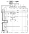
- FIG. 4 is another partial front view of the liquid crystal panel 10 with the CF substrate 21 and the polarizing plate 25 removed.
- FIG. 4 shows a lower left portion of the liquid crystal panel 10.
- a common wiring 38 (second electrode wiring) is formed inside the seal portion 22 in the TFT substrate 20.
- the common wiring 38 extends along the left side portion, the upper side portion, and the right side portion of the seal portion 22 having a rectangular frame shape.
- the common wiring 38 is not disposed at a position along the lower portion of the seal portion 22, that is, below the TFT substrate 20, and has a U shape.
- the seal part 22 has conductivity.
- the common wiring 38 is connected to the common electrode 27 through the seal portion 22 at a plurality of locations, and is connected to the common electrode 27. Thereby, the potential of the entire common electrode 27 is stabilized.
- a plurality (two in the first embodiment) of spare wirings 39a and 39b (inner wirings) are formed on the TFT substrate 20 and the plurality of printed circuit boards 34, 34,.
- the two spare wirings 39a and 39b are juxtaposed.
- Each of the two spare wirings 39a and 39b extends in the left-right direction on the upper side of the TFT substrate 20 between the seal portion 22 and the gate line 30 provided on the uppermost side.
- the two spare wirings 39 a and 39 b pass between the gate driver 35 and the edge of the printed circuit board 34.
- the two spare wirings 39 a, 39 b once enter the inside of the seal portion 22 in the TFT substrate 20 from one printed board 34 and then enter the other printed board 34. Yes.
- the two spare wirings 39 a and 39 b extend in the left-right direction between the seal portion 22 and the gate line 30 provided on the lowermost side.
- the two spare wirings 39 a and 39 b are respectively an upper portion of the seal portion 22, a lower portion of the seal portion 22, a left side portion of the seal portion 22, and It is formed along a part of the right part (a part between adjacent printed circuit boards 34 and 34 and a part below the lowest printed circuit board 34).
- connection wiring 40a for connecting the source line 29 and the spare wiring 39a for each of the M source lines 29, 29,.
- the connection wiring 40a intersects the source line 29 and the spare wiring 39a.
- the connection wiring 40a is separated from the source line 29 and the spare wiring 39a in the front-rear direction.
- the TFT substrate 20 is provided with a connection wiring 40b for connecting the source line 29 and the spare wiring 39b for each of the M source lines 29, 29,.
- the connection wiring 40b intersects the source line 29 and the spare wiring 39b.
- the connection wiring 40b is separated from the source line 29 and the spare wiring 39b in the front-rear direction.
- FIG. 5 is an explanatory diagram of the spare wiring 39a
- FIG. 6 is another explanatory diagram of the spare wiring 39a. 5 corresponds to FIG. 3, and FIG. 6 corresponds to FIG.
- the source driver 32 when a disconnection occurs in the source line 29, the source driver 32 cannot output a voltage to the lower source line 29 among the two source lines 29 and 29 separated by the disconnection. For this reason, the source driver 32 cannot apply a voltage to one or a plurality of pixel electrodes 26, 26,... Connected to the lower source line 29.
- the upper source line 29 is connected to the spare wiring 39a.
- melt connection between the upper source line 29 and the spare wiring 39a is performed using a laser.
- the connection wiring 40a corresponding to the source line 29 where the disconnection has occurred is connected to the lower source line 29 and the spare wiring 39a using, for example, a laser.
- the source driver 32 includes not only one or a plurality of pixel electrodes 26, 26,... Connected to the upper source line 29 but also one or a plurality of pixels connected to the lower source line 29. It is possible to apply a voltage to the pixel electrodes 26, 26,.
- the two source lines 29 and 29 separated by the disconnection can be similarly connected using the spare wiring 39b.
- the upper source line 29 is connected to the spare wiring 39b
- the connection wiring 40b is connected to the lower source line 29 and the spare wiring 39b.
- One or a plurality of (in the first embodiment, a plurality of) conductors 41, 41,... are disposed in contact with the seal portion 22 and the spare wiring 39a.
- the plurality of conductors 41, 41,... are disposed between the spare wiring 39 a and the seal portion 22, and are disposed between the spare wiring 39 b and the seal portion 22.
- the plurality of conductors 41, 41,... are not electrically connected to the other conductors, for example, the entire surfaces of the plurality of conductors 41, 41,. .
- Each of the plurality of conductors 41, 41,... Has a long plate shape, and each of the plurality of conductors 41, 41,.
- the plurality of conductors 41, 41,... are arranged over the entire area surrounded by the seal portion 22 and the spare wiring 39a.
- a width of a part of the conductor 41 is narrower than a part of the conductor 41 other than the part.
- the width of a portion of the conductor 41 is extremely narrow with respect to the width of the conductor 41 other than the portion.
- the width of the central portion 41a in the longitudinal direction of each conductor 41 is narrower than the widths of the two connecting portions 41b and 41b other than the central portion 41a.
- the lower right portion of the TFT substrate 20 is configured similarly to the lower left portion of the TFT substrate 20 shown in FIG.
- the TFT substrate 20 are provided on the upper side of the TFT substrate 20, and a plurality of printed substrates 34, 34,... Are provided on the left and right sides of the TFT substrate 20, respectively. . Accordingly, a part of the electrostatic current that flows through the upper part, the left part, and the right part of the seal portion 22 flows to the printed boards 31 and 34, and the electrostatic current is dispersed. For this reason, although the conductor 41 is not disposed on the upper side, the left side, and the right side of the TFT substrate 20, the amount of static electricity flowing to the spare wirings 39a and 39b is reduced.
- the width of the central portion 41a is narrower than the width of the connecting portions 41b, 41b. Therefore, when an electrostatic current flows through the conductor 41, electric charges are concentrated in the central portion, and electric power is converted into thermal energy. As a result, the electrostatic current flowing through the conductor 41 is reduced, so that the amount of static electricity moving from the conductor 41 to the spare wirings 39a and 39b, that is, the amount of electrostatic current flowing through the spare wirings 39a and 39b can be reduced. Further, in each of the plurality of conductors 41, 41,..., A narrow portion is provided at the center in the longitudinal direction. For this reason, an electric current tends to flow through the narrow central portion 41a. As a result, electric power is efficiently converted into thermal energy, and the current flowing through the conductor 41 is greatly reduced.
- the two diodes D ⁇ b> 1 and D ⁇ b> 2 connect two adjacent spare wirings 39 a and 39 b.
- the anode of the diode D1 and the cathode of the diode D2 are connected to the spare wiring 39a.
- the cathode of the diode D1 and the anode of the diode D2 are connected to the spare wiring 39b.
- the two diodes D1 and D2 form a so-called diode ring.
- the width of the voltage drop that occurs when the current flows in the forward direction is larger than the maximum value of the voltage applied by each of the plurality of source drivers 32, 32,. Therefore, when one source driver 32 is connected to the spare wiring 39a, the source driver 32 does not apply a voltage to the spare wiring 39b via the diode D1. Similarly, when one source driver 32 is connected to the spare wiring 39b, the source driver 32 does not apply a voltage to the spare wiring 39a via the diode D2. In other words, a small current output from each of the plurality of source drivers 32, 32,... Does not flow forward through the diode D1 or D2, and a large current such as an electrostatic current flows forward through the diode D1 or D2. Flowing.
- a substrate wiring 42 is formed along the source line 29 located on the leftmost side.
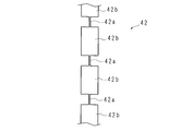
- FIG. 7 is a partially enlarged view of the substrate wiring 42.
- the substrate wiring 42 has a long plate shape, and the plate surface of the substrate wiring 42 faces the rear surface of the CF substrate 21.
- the width of a portion of the substrate wiring 42 is narrower than the width of the portion other than the portion of the substrate wiring 42.
- the width of a portion of the substrate wiring 42 is extremely narrower than the width of the portion other than the portion of the substrate wiring 42.
- the substrate wiring 42 has a plurality of first portions 42a, 42a,... And a plurality of second portions 42b, 42b,.
- the first portions 42a and the second portions 42b are alternately arranged, and the end portions of the first portions 42a are connected to the second portions 42b.
- the width of the first portion 42a is narrower than the width of the second portion 42b. Therefore, when a current flows through the substrate wiring 42, charges are concentrated on the first portion 42 a, and electric power is converted into thermal energy. As a result, even if the generated static electricity flows to the spare wirings 39a and 39b, a part of the static electricity is converted into thermal energy in the process of flowing through the substrate wiring 42 connected to the spare wiring 39b, and the electrostatic current is Get smaller. As a result, it is possible to suppress an electrostatic current from flowing through the source line 29.
- the spare wiring 39b disposed on the innermost side of the TFT substrate 20 and the substrate wiring 42 include a diode D3 (third diode) and a diode D4 ( Connected by a second diode).
- the anode of the diode D3 and the cathode of the diode D4 are connected to the spare wiring 39b.
- the cathode of the diode D3 and the anode of the diode D4 are connected to the substrate wiring 42.
- the substrate wiring 42 is connected only to the diodes D3 and D4.
- the two diodes D3 and D4 constitute a diode ring.
- the substrate wiring 42 and the spare wiring 39b are connected by the diodes D3 and D4. Therefore, when the current flowing through the spare wiring 39b is large, a part of this current flows through the substrate wiring 42, and when the current flowing through the substrate wiring 42 is large, a part of this current flows through the spare wiring 39b. For this reason, it is possible to effectively suppress the electrostatic current from flowing to the source line 29 formed along the substrate wiring 42.
- the substrate wiring is also formed between the source line 29 arranged on the rightmost side in the left-right direction and the seal portion 22 along the source line 29 arranged on the rightmost side. Yes. Further, the substrate wiring and spare wiring 39b are also connected by two diodes in the same manner as the left substrate wiring 42 and spare wiring 39b.
- FIG. 8 is a partial front view of liquid crystal panel 10 according to the second embodiment.
- the differences between the second embodiment and the first embodiment will be described. Since the configuration other than the configuration described later is the same as that in the first embodiment, the same reference numerals as those in the first embodiment are given to the components common to the first embodiment, and the description thereof is omitted. To do.
- FIG. 8 corresponds to FIG. 4, and FIG. 8 shows a lower left portion of the liquid crystal panel 10 from which the CF substrate 21 and the polarizing plate 25 are removed.
- the common wiring 38 is formed inside the seal portion 22 as in the first embodiment.
- the common wiring 38 in the second embodiment is not only on the left side portion, the upper side portion and the right side portion of the seal portion 22 but also on the lower side portion of the seal portion 22 and has an annular shape.
- the common wiring 38 in the second embodiment is connected to the common electrode 27 through the seal portion 22 at a plurality of locations and is electrically connected to the common electrode 27. Thereby, the potential of the entire common electrode 27 is stabilized.
- the numbers of the printed boards 31 and 34, the source driver 32, and the gate driver 35 are not limited to eight, and may be one or more. If the number of source drivers 32 is 1, J matches M. If the number of gate drivers 35 is 1, K matches M. The numbers of the printed circuit boards 31 and 34, the source driver 32, and the gate driver 35 may not be the same. In the conductor 41, the number of narrow portions is not limited to 1, and may be 2 or more.
- FIG. 9 is an external view of the conductor 50 in the third embodiment.
- the differences between the third embodiment and the first embodiment will be described. Since the configuration other than the configuration described later is the same as that in the first embodiment, the same reference numerals as those in the first embodiment are given to the components common to the first embodiment, and the description thereof is omitted. To do.
- the liquid crystal panel 10 in the third embodiment has a conductor 50 instead of the conductor 41.
- the plurality of conductors 41, 41,... In the first embodiment are replaced with the conductors 50.
- the conductor 50 in the third embodiment has a long plate shape like the conductor 41 in the first embodiment.
- the plate surface of the conductor 50 faces the rear surface of the CF substrate 21.
- the plurality of conductors 50, 50,... Are arranged along the lower part of the seal portion 22.
- the widths of both end portions 50a and 50a are narrower than the width of the connecting portion 50b which is a portion other than the end portions 50a and 50a.
- the width of the end portion 50a is extremely narrow with respect to the width of the connecting portion 50b. For this reason, when an electric current flows through the conductor 50, electric charge concentrates in each of the end portions 50a and 50a, and electric power is converted into thermal energy. As a result, the electrostatic current flowing through the conductor 50 is reduced, so that the amount of static electricity moving from the conductor 50 to the spare wirings 39a and 39b, that is, the amount of electrostatic current flowing through the spare wirings 39a and 39b can be reduced.
- the liquid crystal panel 10 according to the third embodiment also exhibits other effects than the effects obtained by the shape of the conductor 41 among the effects exhibited by the liquid crystal panel 10 according to the first embodiment.
- the conductor 41 may be replaced with the conductor 50 in the third embodiment.
- the liquid crystal panel 10 configured in this way also has the same effect as the liquid crystal panel 10 in the third embodiment.
- the portion may be replaced with the conductor 50 in the third embodiment.
- FIG. 10 is an external view of the conductor 60 in the fourth embodiment.
- the differences between the fourth embodiment and the first embodiment will be described. Since the configuration other than the configuration described later is the same as that in the first embodiment, the same reference numerals as those in the first embodiment are given to the components common to the first embodiment, and the description thereof is omitted. To do.
- the liquid crystal panel 10 according to the fourth embodiment has a conductor 60 instead of the conductor 41.
- the plurality of conductors 41, 41,... In the first embodiment are replaced with conductors 60.
- the conductor 60 in the fourth embodiment has a long plate shape like the conductor 41 in the first embodiment.
- the plate surface of the conductor 60 faces the rear surface of the CF substrate 21.
- the plurality of conductors 60, 60,... Are arranged along the lower part of the seal portion 22.
- An opening 60 a is provided in the central portion of the conductor 60.
- the width of the central portion (two first portions 60b and 60b) is narrower than the two second portions 60c and 60c other than the central portion.
- the width of the central portion of the conductor 60 is extremely narrow with respect to the width of the portion other than the central portion. For this reason, when an electric current flows through the conductor 60, electric charges concentrate in each of the first portions 60b and 60b, and electric power is converted into thermal energy.
- the electrostatic current flowing through the conductor 60 is reduced, so that the amount of static electricity moving from the conductor 60 to the spare wirings 39a and 39b, that is, the amount of electrostatic current flowing through the spare wirings 39a and 39b can be reduced.
- the liquid crystal panel 10 according to the fourth embodiment also exhibits other effects than the effects obtained by the shape of the conductor 41 among the effects exhibited by the liquid crystal panel 10 according to the first embodiment.
- the number of openings 60a is not limited to 1, and may be 2 or more.
- the conductor 41 may be replaced with the conductor 60 in the fourth embodiment.
- the liquid crystal panel 10 configured in this way also has the same effect as the liquid crystal panel 10 in the fourth embodiment.
- the portion may be replaced with the conductor 60 in the fourth embodiment.
- the shape of the conductor is a shape having at least two of the characteristics of the conductor 41 of the first embodiment, the conductor 50 of the third embodiment, and the conductor 60 of the fourth embodiment. Also good. Moreover, the shape of each of the plurality of conductors may not be the same. Furthermore, the number of conductors may be one.
- FIG. 11 is a partially enlarged view of the substrate wiring 70 in the fifth embodiment.
- the difference between the fifth embodiment and the first embodiment will be described. Since the configuration other than the configuration described later is the same as that in the first embodiment, the same reference numerals as those in the first embodiment are given to the components common to the first embodiment, and the description thereof is omitted. To do.
- the liquid crystal panel 10 according to the fifth embodiment has a substrate wiring 70 instead of the substrate wiring 42.
- the substrate wiring 42 in the first embodiment is replaced with the substrate wiring 70.
- the substrate wiring 70 in the fifth embodiment has a long plate shape like the substrate wiring 42 in the first embodiment, and the plate surface of the substrate wiring 70 faces the rear surface of the CF substrate 21.
- a plurality of openings 70 a, 70 a,... are sequentially provided along the longitudinal direction of the substrate wiring 70.
- the substrate wiring 70 has a plurality of first portions 70b, 70b,... And a plurality of second portions 70c, 70c,.
- a plurality of second portions 70 c, 70 c,... are also sequentially provided along the longitudinal direction of the substrate wiring 70.
- Two adjacent second parts 70c and 70c are connected by two first parts 70b and 70b.
- the width of the first portion 70b is narrower than the width of the second portion 70c, which is a portion other than the first portion 70b. Therefore, when current flows through the substrate wiring 70, electric charges concentrate on the first portion 70b, and electric power is converted into thermal energy. Thereby, the electrostatic current flowing through the substrate wiring 70 is reduced. As a result, the flow of electrostatic current can be suppressed.
- the liquid crystal panel 10 according to the fifth embodiment configured as described above has the same effects as those of the first embodiment.
- FIG. 12 is a partial front view of liquid crystal panel 10 in the sixth embodiment.
- the difference between the sixth embodiment and the first embodiment will be described. Since the configuration other than the configuration described later is the same as that in the first embodiment, the same reference numerals as those in the first embodiment are given to the components common to the first embodiment, and the description thereof is omitted. To do.
- a single conductor 90 is arranged on the TFT substrate 20 of the liquid crystal panel 10 in the sixth embodiment instead of the conductors 41, 41,.
- the conductor 90 is disposed between the spare wiring 39 a and the seal portion 22, and is disposed between the spare wiring 39 b and the seal portion 22.
- the conductor 90 is not electrically connected to other conductors. For example, the entire surface of the conductor 90 is covered with an insulator.
- the conductor 90 has a plate shape, and the plate surface of the conductor 90 faces the rear surface of the CF substrate 21.
- the conductor 90 is disposed over the entire area surrounded by the seal portion 22 and the spare wiring 39a.
- a width of a part of the conductor 90 is narrower than a width of a part of the conductor 90 other than the part.
- the width of a part of the conductor 90 is extremely narrow with respect to the width of a part of the conductor 90 other than the part.
- the conductor 90 has a plurality of first portions 90a, 90a,... And a plurality of second portions 90b, 90b,. In the conductor 90, the first portions 90a and the second portions 90b are alternately arranged, and the first portions 90a are connected to the second portions 90b.
- the width of the first portion 90a is narrower than the width of the second portion 90b.
- the width of the first portion 90a is narrower than the width of the second portion 90b. Therefore, when an electrostatic current flows through the conductor 90, electric charges are concentrated in the first portion 90a, and electric power is converted into thermal energy. As a result, the electrostatic current flowing through the conductor 90 is reduced, so that the amount of static electricity moving from the conductor 90 to the spare wirings 39a and 39b, that is, the amount of electrostatic current flowing through the spare wirings 39a and 39b can be reduced.
- the liquid crystal panel 10 according to the sixth embodiment also exhibits other effects than the effects obtained by arranging the plurality of conductors 41, 41,... Among the effects exhibited by the liquid crystal panel 10 according to the first embodiment. .
- the plurality of conductors 41, 41,... May be replaced with one conductor 90.
- the number of first portions 42a of the substrate wiring 42 may be one.
- the number of openings 70a may be one.
- the substrate wiring 42 may be replaced with the substrate wiring 70 in the fifth embodiment.
- the shape of the substrate wiring may be a shape having the characteristics of the substrate wiring 42 of the first embodiment and the substrate wiring 70 of the fifth embodiment.
- the shape of the end portion of the substrate wiring may be the same as the shape of the end portion 50a of the conductor 50 in the third embodiment.
- the number of spare wirings is not limited to 2, and may be 1 or 3 or more.
- the number of spare wirings is 3 or more, these spare wirings are also juxtaposed, and the above-described diode ring is configured between adjacent spare wirings. Therefore, the number of diode rings is ((number of spare wirings) -1) or more. Further, a diode ring is formed between the spare wiring located on the innermost side of the TFT substrate 20 and the substrate wiring 42.
- the number of connection lines formed for each of the plurality of source lines 29, 29,... Is the same as the number of spare lines.
Landscapes
- Physics & Mathematics (AREA)
- Nonlinear Science (AREA)
- Mathematical Physics (AREA)
- Chemical & Material Sciences (AREA)
- Crystallography & Structural Chemistry (AREA)
- General Physics & Mathematics (AREA)
- Optics & Photonics (AREA)
- Engineering & Computer Science (AREA)
- Microelectronics & Electronic Packaging (AREA)
- Geometry (AREA)
- Liquid Crystal (AREA)
- Devices For Indicating Variable Information By Combining Individual Elements (AREA)
Abstract
TFT基板(20)及びCF基板の周縁に沿って配置されたシール部(22)を介して、TFT基板(20)及びCF基板が間隔を空けて連結されている。シール部(22)の内側に液晶が封入されている。TFT基板(20)におけるシール部(22)の内側において、予備配線(39a,39b)は、シール部(22)に沿って形成されている。TFT基板(20)において、導体(41)は、シール部(22)及び予備配線(39a,39b)間に、シール部(22)及び予備配線(39a,39b)と非接触で配置されている。
Description
本発明は、2つの基板間に液晶が封入されている液晶パネル、及び、該液晶パネルを備える表示装置に関する。
画像を表示する液晶表示装置は液晶パネルを備える(例えば、特許文献1)。特許文献1に記載の液晶パネルでは、2つの基板が、該基板の周縁に沿って配置されたシールによって間隔を空けて連結されている。シールの内側(シールによって囲まれた領域)には液晶が封入されている。
2つの基板中の一方の基板には、複数の画素電極が形成されている。他方の基板には共通電極が形成されている。複数の画素電極夫々は共通電極と対向している。共通電極の電位を基準として、画素電極に電圧を印加する。画素電極に印加されている電圧に応じて、液晶分子の状態が異なる。液晶分子の状態に応じて、画素電極を介して液晶パネルの外側に出射される光の強度が決まる。画像データに応じた電圧を複数の画素電極夫々に印加することによって、液晶パネルに、画像データに基づく画像が表示される。
一方の基板には、共通電極に導通する共通配線(Vcom配線)がシールに沿って形成されている。特許文献1に記載の液晶パネルでは、共通配線よりも外側に外側配線(GND配線)が更に設けられている。従って、例えば、人体が液晶パネルに触れることで静電気放電(ESD)が発生した場合でも、静電気が流れることにより生じた電流(以下、静電気電流という)は、外側配線を流れ、共通配線に流れることはない。これにより、共通配線の近傍に配置された回路又は配線等に静電気電流が流れることはない。結果、回路の動作不良、配線の断線、又は、隣り合う配線の融着等の発生が防止される。
静電気は、液晶パネルの製造過程においても発生する。液晶パネルでは、共通電極が形成された基板の板面に偏光板が貼り付けられている。例えば、偏光板と基板との間に異物が混入している場合、又は、偏光板に傷がある場合、偏光板が基板から剥がされて、新たな偏光板が貼り付けられる。偏光板が基板から剥がされた場合、静電気が発生する。
従来の液晶パネルとして、共通配線が、シールを介して共通電極に導通し、シールの内側において、複数の内側配線が共通配線の近傍に形成されている液晶パネルがある。これらの内側配線は、例えば、複数の画素電極に接続されている配線が断線した場合に、断線によって分かれた2つの配線を接続するために用いられる予備配線である。
以上のような液晶パネルにおいて、共通電極が形成されている基板から偏光板が剥がされた場合に発生した静電気は、シールを通じて共通配線に流れ、更には、共通配線から内側配線に移動して、内側配線に大きな電流(静電気電流)が流れる。これにより、内側配線の断線、又は、隣接する2つの内側配線の融着等が発生することがある。また、静電気が内側配線からアクティブエリア内の配線(ソース線又はゲート線)まで流れて、アクティブエリア内の配線や回路素子を破壊することもある。
特に、画像が表示されない非表示領域が狭い狭額縁の液晶パネルでは、共通配線及び内側配線間の距離が短い。このため、静電気電流が内側配線に流れ易く、回路の破壊(内側配線の断線又は融着等)を引き起こし易い。
本発明は斯かる事情に鑑みてなされたものであり、その目的とするところは、静電気による回路の破壊を抑制し得る液晶パネル及び該液晶パネルを備える表示装置を提供することにある。
本発明に係る液晶パネルは、2つの基板間に該基板の周縁に沿って配置された連結部材を介して、該2つの基板が間隔を空けて連結されており、該連結部材の内側に液晶が封入されている液晶パネルにおいて、前記2つの基板中の一方の基板における前記連結部材の内側にて、該連結部材に沿って形成されている内側配線と、前記一方の基板にて、前記連結部材及び内側配線間に、前記連結部材及び内側配線と非接触で配置された導体とを備えることを特徴とする。
本発明に係る表示装置は、前述した液晶パネルと、該液晶パネルに光を照射する照射部とを備え、前記液晶パネルは、該照射部が照射した光を用いて画像を表示することを特徴とする。
本発明によれば、静電気による回路の破壊を抑制し得る液晶パネル及び該液晶パネルを備える表示装置が提供される。
以下、本発明の実施の形態について図面に基づいて詳述する。
(実施の形態1)
図1は実施の形態1における表示装置1の概略図である。表示装置1は、矩形板状の液晶パネル10及びバックライト装置11を備える。図1には液晶パネル10の縦断面が示されている。バックライト装置11(照射部)は液晶パネル10に光を照射する。液晶パネル10は、バックライト装置11が照射した光を用いて画像を表示する。
(実施の形態1)
図1は実施の形態1における表示装置1の概略図である。表示装置1は、矩形板状の液晶パネル10及びバックライト装置11を備える。図1には液晶パネル10の縦断面が示されている。バックライト装置11(照射部)は液晶パネル10に光を照射する。液晶パネル10は、バックライト装置11が照射した光を用いて画像を表示する。
図2は液晶パネル10の正面図である。図1及び図2に示すように、液晶パネル10は、バックライト装置11が照射した光が入射される矩形状のTFT基板20と、光を出射する矩形状のCF基板21とを有する。TFT基板20は、複数の画素電極26,26,・・・、複数のTFT(Thin Film Transistor)28,28,・・・等を備え(図3参照)、CF基板21は、共通電極27(第2の電極)、図示しないカラーフィルタ等を備える。バックライト装置11が照射した光は、TFT基板20の後面から入射され、CF基板21の前面から出射される。TFT基板20及びCF基板21夫々は、透明であり、例えばガラスによって構成されている。
TFT基板20の前面はCF基板21の後面に対向している。TFT基板20及びCF基板21間には、TFT基板20及びCF基板21の周縁に沿って矩形枠状のシール部22(連結部材)が配置されている。シール部22は、TFT基板20及びCF基板21の全周に亘って連続している。TFT基板20及びCF基板21は、シール部22を介して、間隔を空けて連結されている。シール部22はTFT基板20及びCF基板21に接着している。これにより、TFT基板20及びCF基板21の連結が実現されている。シール部22の内側(シール部22によって囲まれた領域)には、液晶23が封入されている。
TFT基板20の後面に偏光板24が貼り付けられている。バックライト装置11が照射した光は、偏光板24及びTFT基板20の順に透過する。偏光板24は、バックライト装置11が照射した光の中で、電界が特定の方向に振動する光のみを透過させる。
同様に、CF基板21の前面の全体に偏光板25が貼り付けられている。バックライト装置11が照射した光は、偏光板24、TFT基板20、液晶23、CF基板21及び偏光板25の順に透過する。偏光板25は、CF基板21を透過した光の中で、電界が特定の方向に振動する光のみを透過させる。
同様に、CF基板21の前面の全体に偏光板25が貼り付けられている。バックライト装置11が照射した光は、偏光板24、TFT基板20、液晶23、CF基板21及び偏光板25の順に透過する。偏光板25は、CF基板21を透過した光の中で、電界が特定の方向に振動する光のみを透過させる。
偏光板24に係る特定の方向は、偏光板25に係る特定の方向と同一方向であってもよいし、偏光板25に係る特定の方向と異なっていてもよい。
図3はCF基板21及び偏光板25が取り外された液晶パネル10の部分正面図である。図3には、前側から見た液晶パネル10の左上部分が示されている。2つの線の接続は黒丸で示されている。黒丸が示されていない2つの線の交点は非接続を示す。
図3に示すように、TFT基板20におけるシール部22の内側には、複数の画素電極26,26,・・・が格子状に形成されている。複数の画素電極26,26,・・・は、透明であり、左右方向及び上下方向に並んでいる。複数の画素電極26,26,・・・夫々は板状をなし、複数の画素電極26,26,・・・夫々の板面は、CF基板21の後面と対向している。図1に示すように、CF基板21には、板状の共通電極27が形成されている。共通電極27も透明である。共通電極27の板面は、全ての画素電極26,26,・・・の板面に対向している。
共通電極27の電位を基準として、複数の画素電極26,26,・・・に電圧を各別に印加する。これにより、液晶23に電圧が印加される。複数の画素電極26,26,・・・及び共通電極27は、液晶23に電圧を印加するために形成されている。図2では、共通電極27の記載を省略している。
複数の画素電極26,26,・・・夫々に印加されている電圧に応じて、複数の画素電極26,26,・・・夫々に対応する液晶23の液晶分子の状態が異なる。液晶分子の状態に応じて、液晶23を透過した光に係る電界の振動方向が異なる。電界の振動方向に応じて、偏光板25から出射される光の強度が異なる。複数の画素電極26,26,・・・夫々に印加している電圧を調整することによって、複数の画素電極26,26,・・・を介して偏光板25から出射される光の強度を調整する。
複数の画素電極26,26,・・・に電圧を適切に印加するために、複数のTFT28,28,・・・がTFT基板20に設けられている。複数の画素電極26,26,・・・夫々には、TFT28のドレインが接続されている。画素電極26の数はTFT28の数と同じである。
TFT28はスイッチとして機能する。TFT28のゲートの電圧が一定電圧以上である場合、TFT28はオンである。TFT28がオンである場合、ドレイン及びソースを介して画素電極26に電圧を印加することが可能である。TFT28のゲートの電圧が一定電圧未満である場合、TFT28はオフである。TFT28がオフである場合、ドレイン及びソースを介して画素電極26に電圧が印加されることはない。
TFT28はスイッチとして機能する。TFT28のゲートの電圧が一定電圧以上である場合、TFT28はオンである。TFT28がオンである場合、ドレイン及びソースを介して画素電極26に電圧を印加することが可能である。TFT28のゲートの電圧が一定電圧未満である場合、TFT28はオフである。TFT28がオフである場合、ドレイン及びソースを介して画素電極26に電圧が印加されることはない。
TFT基板20では、上下方向に延びるM(M:2以上の整数)個のソース線29,29,・・・(電極配線)が左右方向に並設されている。M個のソース線29,29,・・・夫々は、自身に対応する縦方向の画素電極群の近傍(図3の例では左側)に配置されている。ここで、縦方向の画素電極群とは、上下方向に並んだ複数の画素電極26,26,・・・のことであり、M個の縦方向の画素電極群は、左右方向に並設されている。M個のソース線29,29,・・・夫々は、自身に対応する縦方向の画素電極群に属する複数の画素電極26,26,・・・にドレインが接続されている複数のTFT28,28,・・・にも対応する。M個のソース線29,29,・・・夫々は、自身に対応する複数のTFT28,28,・・・夫々のソースに接続されている。
従って、M個のソース線29,29,・・・夫々は、自身に対応する複数のTFT28,28,・・・を介して、自身に対応する縦方向の画素電極群に属する複数の画素電極26,26,・・・に接続されている。
従って、M個のソース線29,29,・・・夫々は、自身に対応する複数のTFT28,28,・・・を介して、自身に対応する縦方向の画素電極群に属する複数の画素電極26,26,・・・に接続されている。
更に、TFT基板20では、左右方向に延びるN(N:2以上の整数)個のゲート線30,30,・・・が上下方向に並設されている。N個のゲート線30,30,・・・夫々は、自身に対応する横方向の画素電極群の近傍(図3の例では上側)に配置されている。ここで、横方向の画素電極群とは、左右方向に並んだ複数の画素電極26,26,・・・のことであり、N個の横方向の画素電極群は、上下方向に並設されている。N個のゲート線30,30,・・・夫々は、自身に対応する横方向の画素電極群に属する複数の画素電極26,26,・・・にドレインが接続されている複数のTFT28,28,・・・にも対応する。N個のゲート線30,30,・・・夫々は、自身に対応する複数のTFT28,28,・・・夫々のゲートに接続されている。
図2及び図3に示すように、TFT基板20の前面における上側部分から複数のプリント基板31,31,・・・夫々が上側に突出している。複数のプリント基板31,31,・・・夫々にはソースドライバ32が実装されている。複数のプリント基板31,31,・・・は、更に、信号基板33に連結されている。図3では、信号基板33の記載を省略している。図2には、プリント基板31及びソースドライバ32夫々の数が8である例が示されている。
複数のソースドライバ32,32,・・・夫々には、J(J:M未満の自然数)個のソース線29,29,・・・が各別に接続されている。図3では、Jが3である例が示されている。複数のソースドライバ32,32,・・・夫々は、自身に接続されているJ個のソース線29,29,・・・に電圧を各別に出力する。ソース線29に電圧が出力された場合、このソース線29に接続されている複数のTFT28,28,・・・の中で、オンである一又は複数のTFT28,28,・・・に接続されている一又は複数の画素電極26,26,・・・に電圧が印加される。
図2及び図3に示すように、TFT基板20の左側及び右側から複数のプリント基板34,34,・・・が突出している。複数のプリント基板34,34,・・・夫々にはゲートドライバ35が実装されている。図2には、プリント基板34及びゲートドライバ35夫々の数が8である例が示されている。
複数のゲートドライバ35,35,・・・夫々には、K(K:N未満の自然数)個のゲート線30,30,・・・が各別に接続されている。図3では、Kが3である例が示されている。複数のゲートドライバ35,35,・・・夫々は、自身に接続されているK個のゲート線30,30,・・・に電圧を各別に出力する。ゲート線30の電圧が一定電圧以上である場合、このゲート線30に接続されている全てのTFT28,28,・・・はオンである。ゲート線30の電圧が一定電圧未満である場合、このゲート線30に接続されている全てのTFT28,28,・・・はオフである。
信号基板33には、制御部36及びタイミングコントローラ37が設けられている。制御部36には、音声データと画像データとが含まれている音声画像信号、例えば、テレビジョン放送に係る放送信号が入力される。制御部36は、音声画像信号から画像データを抽出し、抽出した画像データをタイミングコントローラ37に出力する。タイミングコントローラ37は、制御部36から入力された画像データに基づいて、各ソース線29に印加すべき電圧、及び、各ゲート線30に電圧を印加すべきタイミング等を示す制御信号を生成する。タイミングコントローラ37は、生成した制御信号を、複数のソースドライバ32,32,・・・及び複数のゲートドライバ35,35,・・・に出力する。
複数のソースドライバ32,32,・・・は、タイミングコントローラ37から入力された制御信号に従って、M個のソース線29,29,・・・に電圧を印加する。複数のゲートドライバ35,35,・・・は、タイミングコントローラ37から入力された制御信号に従って、N個のゲート線30,30,・・・に電圧を印加する。これにより、複数の画素電極26,26,・・・には、電圧が各別に印加され、各画素電極26を介して偏光板25から出射される光の強度が、制御部36がタイミングコントローラ37に出力した画像データに応じて調整される。結果、画像データに基づく画像が液晶パネル10に表示される。
図4は、CF基板21及び偏光板25が取り外された液晶パネル10の他の部分正面図である。図4には、液晶パネル10の左下部分が示されている。図3及び図4に示すように、TFT基板20におけるシール部22の内側に、共通配線38(第2の電極配線)が形成されている。共通配線38は、矩形枠状のシール部22の左側部分、上側部分及び右側部分に沿っている。実施の形態1において、共通配線38は、シール部22の下側部分に沿った位置、即ち、TFT基板20の下側に配置されておらず、U字状をなしている。
シール部22は導電性を有する。共通配線38は、複数の箇所でシール部22を介して共通電極27に接続され、共通電極27に導通している。これにより、共通電極27全体の電位が安定する。
TFT基板20、及び、複数のプリント基板34,34,・・・には、複数(実施の形態1では2つ)の予備配線39a,39b(内側配線)が形成されている。2つの予備配線39a,39bは並置されている。2つの予備配線39a,39b夫々は、TFT基板20の上側において、シール部22と、最も上側に設けられているゲート線30との間を、左右方向に延びている。プリント基板34では、2つの予備配線39a,39bは、ゲートドライバ35とプリント基板34の縁との間を通っている。隣り合うプリント基板34,34間では、2つの予備配線39a,39bは、一方のプリント基板34から、一旦、TFT基板20におけるシール部22の内側に入った後、他方のプリント基板34に入っている。TFT基板20の下側において、2つの予備配線39a,39bは、シール部22と、最も下側に設けられているゲート線30との間を、左右方向に延びている。
以上のように、TFT基板20におけるシール部22の内側において、2つの予備配線39a,39b夫々は、シール部22の上側部分と、シール部22の下側部分と、シール部22の左側部分及び/又は右側部分の一部(隣り合うプリント基板34,34間の部分、及び最も下側にあるプリント基板34よりも下側の部分)に沿って形成されている。
以上のように、TFT基板20におけるシール部22の内側において、2つの予備配線39a,39b夫々は、シール部22の上側部分と、シール部22の下側部分と、シール部22の左側部分及び/又は右側部分の一部(隣り合うプリント基板34,34間の部分、及び最も下側にあるプリント基板34よりも下側の部分)に沿って形成されている。
図4に示すように、TFT基板20には、M個のソース線29,29,・・・夫々について、該ソース線29と予備配線39aとを接続させるための接続配線40aが設けられている。前側から液晶パネル10を見た場合、接続配線40aは、ソース線29及び予備配線39a夫々と交差している。ただし、接続配線40aは、ソース線29及び予備配線39a夫々と前後方向に離れている。
同様に、TFT基板20には、M個のソース線29,29,・・・夫々について、該ソース線29と予備配線39bとを接続させるための接続配線40bが設けられている。前側から液晶パネル10を見た場合、接続配線40bは、ソース線29及び予備配線39b夫々と交差している。ただし、接続配線40bは、ソース線29及び予備配線39b夫々と前後方向に離れている。
2つの予備配線39a,39b夫々は、ソース線29に断線が発生した場合に用いられる。図5は予備配線39aの説明図であり、図6は予備配線39aの他の説明図である。図5は図3に対応し、図6は図4に対応する。
図5に示すように、ソース線29に断線が発生した場合、ソースドライバ32は、断線によって分かれた2つのソース線29,29中の下側のソース線29に電圧を出力することはできない。このため、ソースドライバ32は、下側のソース線29に接続されている一又は複数の画素電極26,26,・・・に電圧を印加することができない。
そこで、図5に示すように、断線によって分かれた2つのソース線29,29の中で、上側のソース線29を予備配線39aに接続させる。例えば、レーザを用いて、上側のソース線29と予備配線39aとのメルト接続を行う。更に、図6に示すように、断線が発生したソース線29に対応する接続配線40aを、例えばレーザを用いて、下側のソース線29と、予備配線39aとに接続させる。これにより、ソースドライバ32は、上側のソース線29に接続されている一又は複数の画素電極26,26,・・・だけではなく、下側のソース線29に接続されている一又は複数の画素電極26,26,・・・にも電圧を印加することが可能となる。
ここでは、予備配線39aを用いる例を示したが、予備配線39bを用いて、断線によって分かれた2つのソース線29,29を同様に接続することができる。この場合、上側のソース線29を予備配線39bに接続させ、接続配線40bを、下側のソース線29と、予備配線39bとに接続させる。
図4に示すように、TFT基板20では、2つの予備配線39a,39bの中で、最も下側を左右方向に通っている予備配線39aと、シール部22の下側部分との間に、シール部22及び予備配線39aと非接触で、一又は複数(実施の形態1では複数)の導体41,41,・・・が配置されている。複数の導体41,41,・・・夫々は、予備配線39aとシール部22との間に配置されていると共に、予備配線39bとシール部22との間に配置されている。複数の導体41,41,・・・夫々は、他の導体に電気的に接続されておらず、例えば、複数の導体41,41,・・・夫々の全面は、絶縁体によって覆われている。
複数の導体41,41,・・・夫々は長板状をなし、複数の導体41,41,・・・夫々の板面は、CF基板21の後面に対向している。複数の導体41,41,・・・は、シール部22と予備配線39aとで囲まれた領域の全体に亘って配置されている。複数の導体41,41,・・・夫々において、該導体41の一部分の幅は、該導体41における該一部分以外の部分よりも狭い。好ましくは、導体41の一部分の幅は、該導体41における該一部分以外の部分の幅に対して極端に狭い。実施の形態1では、各導体41の長手方向の中央部分41aの幅は、中央部分41a以外の2つの連結部分41b,41b夫々の幅よりも狭い。
TFT基板20の右下部分は、図4に示されているTFT基板20の左下部分と同様に構成されている。
TFT基板20の右下部分は、図4に示されているTFT基板20の左下部分と同様に構成されている。
液晶パネル10の製造過程において、例えば、CF基板21及び偏光板25間に異物が混入されている場合、又は、偏光板25に傷がある場合、偏光板25をCF基板21から剥がす作業が行われる。このとき、CF基板21側に静電気が発生する。発生した静電気はシール部22を伝ってTFT基板20側へ流れる。TFT基板20の下側部分においては、発生した静電気は、シール部22の近傍に配置されている複数の導体41,41,・・・中の少なくとも1つに移動して、導体41上を流れる。そのため、シール部22の下側部分を介して予備配線39a,39bへ流れる静電気の量を低減させることができる。従って、静電気によって、予備配線39a,39b又はアクティブエリア内の配線(ソース線29若しくはゲート線30)が断線又は融着すること、更には、静電気によってTFT28等の回路素子が破壊されることを抑制することができる。
なお、TFT基板20の上側には複数のプリント基板31,31,・・・が設けられ、TFT基板20の左側及び右側夫々には複数のプリント基板34,34,・・・が設けられている。従って、シール部22の上側部分、左側部分及び右側部分を流れた静電気電流の一部はプリント基板31,34に流れ、静電気電流が分散される。このため、TFT基板20の上側、左側及び右側においては、導体41は配置されていないものの、予備配線39a,39bへ流れる静電気の量が低減される。
また、複数の導体41,41,・・・夫々において、中央部分41aの幅は、連結部分41b,41bの幅よりも狭い。従って、静電気電流が導体41を流れる場合、中央部分において、電荷が集中し、電力が熱エネルギーに変換される。これにより、導体41を流れる静電気電流は小さくなるので、導体41から予備配線39a,39bへ移動する静電気の量、つまり予備配線39a,39bを流れる静電気電流の量を低減させることができる。
更に、複数の導体41,41,・・・夫々において、幅が狭い部分が長手方向の中央部に設けられている。このため、幅が狭い中央部分41aに電流が流れ易い。結果、電力が効率的に熱エネルギーに変換され、導体41を流れる電流が大きく低下する。
更に、複数の導体41,41,・・・夫々において、幅が狭い部分が長手方向の中央部に設けられている。このため、幅が狭い中央部分41aに電流が流れ易い。結果、電力が効率的に熱エネルギーに変換され、導体41を流れる電流が大きく低下する。
図4に示すように、TFT基板20では、2つのダイオードD1,D2は、隣接する2つの予備配線39a,39bを接続している。ダイオードD1のアノード、及び、ダイオードD2のカソードは、予備配線39aに接続されている。ダイオードD1のカソード、及び、ダイオードD2のアノードは、予備配線39bに接続されている。このように、2つのダイオードD1,D2は、所謂ダイオードリングを構成している。
ダイオードD1,D2において、電流が順方向に流れた場合に生じる電圧降下の幅は、複数のソースドライバ32,32,・・・夫々が印加する電圧の最大値よりも大きい。このため、一のソースドライバ32が予備配線39aに接続されている場合、このソースドライバ32がダイオードD1を介して予備配線39bに電圧を印加することはない。同様に、一のソースドライバ32が予備配線39bに接続されている場合、このソースドライバ32がダイオードD2を介して予備配線39aに電圧を印加することはない。言い換えると、複数のソースドライバ32,32,・・・夫々が出力した小さな電流がダイオードD1又はD2を順方向に流れることはなく、静電気電流のような大きな電流がダイオードD1又はD2を順方向に流れる。
隣接する2つの予備配線39a,39bが2つのダイオードD1,D2夫々によって接続されているので、隣接する2つの予備配線39a,39b中の一方の予備配線に流れる電流が大きい場合、この電流の一部が、他方の予備配線に流れる。このため、たとえ静電気電流が予備配線39a又は39bに流れた場合であっても、静電気電流は2つの予備配線39a,39b間で分散されるので、予備配線39a,39bの断線又は融着等の発生を効果的に抑制することができる。
図3及び図4に示すように、TFT基板20では、複数のソース線29,29,・・・の並設方向、即ち、左右方向の最も左側に位置するソース線29と、シール部22との間に基板配線42が、最も左側に位置するソース線29に沿って形成されている。
図7は基板配線42の部分拡大図である。基板配線42は長板状をなし、基板配線42の板面はCF基板21の後面と対向している。基板配線42の一部分の幅は、基板配線42における該一部分以外の部分の幅よりも狭い。好ましくは、基板配線42の一部分の幅は、基板配線42における該一部分以外の部分の幅に対して極端に狭い。実施の形態1では、基板配線42は、複数の第1部分42a,42a,・・・と、複数の第2部分42b,42b,・・・とを有する。基板配線42では、第1部分42a及び第2部分42bは交互に配置され、第1部分42aの端部は第2部分42bに連結されている。第1部分42aの幅は、第2部分42bの幅よりも狭い。
従って、電流が基板配線42を流れる場合、第1部分42aに電荷が集中し、電力が熱エネルギーに変換される。これにより、発生した静電気が予備配線39a,39bまで流れてきた場合でも、その後、静電気の一部は、予備配線39bに接続された基板配線42を流れる過程で熱エネルギーに変換され、静電気電流は小さくなる。結果、ソース線29に静電気電流が流れることを抑制することができる。
従って、電流が基板配線42を流れる場合、第1部分42aに電荷が集中し、電力が熱エネルギーに変換される。これにより、発生した静電気が予備配線39a,39bまで流れてきた場合でも、その後、静電気の一部は、予備配線39bに接続された基板配線42を流れる過程で熱エネルギーに変換され、静電気電流は小さくなる。結果、ソース線29に静電気電流が流れることを抑制することができる。
図4に示すように、2つの予備配線39a,39bの中で、TFT基板20の最も内側に配置された予備配線39bと、基板配線42とがダイオードD3(第3のダイオード)及びダイオードD4(第2のダイオード)によって接続されている。ダイオードD3のアノードと、ダイオードD4のカソードとが予備配線39bに接続されている。ダイオードD3のカソードと、ダイオードD4のアノードとが基板配線42に接続されている。基板配線42は、ダイオードD3,D4のみに接続されている。2つのダイオードD3,D4はダイオードリングを構成している。
前述したように、基板配線42と予備配線39bとがダイオードD3,D4によって接続されている。このため、予備配線39bを流れる電流が大きい場合、この電流の一部が基板配線42に流れ、基板配線42を流れる電流が大きい場合、この電流の一部が予備配線39bに流れる。このため、静電気電流が基板配線42に沿って形成されているソース線29に流れることを効果的に抑制することができる。
なお、TFT基板20では、左右方向の最も右側に配置されているソース線29と、シール部22との間にも基板配線が、最も右側に配置されているソース線29に沿って形成されている。更に、この基板配線及び予備配線39bも2つのダイオードによって、左側の基板配線42及び予備配線39bと同様に接続されている。
(実施の形態2)
図8は、実施の形態2における液晶パネル10の部分正面図である。
以下では、実施の形態2について、実施の形態1と異なる点を説明する。後述する構成を除く他の構成については、実施の形態1と共通しているため、実施の形態1と共通する構成部には実施の形態1と同一の参照符号を付してその説明を省略する。
図8は、実施の形態2における液晶パネル10の部分正面図である。
以下では、実施の形態2について、実施の形態1と異なる点を説明する。後述する構成を除く他の構成については、実施の形態1と共通しているため、実施の形態1と共通する構成部には実施の形態1と同一の参照符号を付してその説明を省略する。
図8は図4に対応し、図8には、CF基板21及び偏光板25が取り外された液晶パネル10の左下部分が示されている。実施の形態2における液晶パネル10では、実施の形態1と同様に、シール部22の内側に共通配線38が形成されている。実施の形態2における共通配線38は、シール部22の左側部分、上側部分及び右側部分だけではなく、シール部22の下側部分にも沿っており、環状をなしている。
実施の形態2における共通配線38は、実施の形態1と同様に、複数の箇所でシール部22を介して共通電極27に接続され、共通電極27に導通している。これにより、共通電極27全体の電位が安定する。
図8に示すように、実施の形態2では、2つの予備配線39a,39bの中で、最も下側を左右方向に通っている予備配線39aと、共通配線38との間に複数の導体41,41,・・・が配置されている。従って、複数の導体41,41,・・・夫々は、予備配線39aと、共通配線38との間に配置されている。
以上のように構成された実施の形態2における液晶パネル10は、実施の形態1における液晶パネル10と同様の効果を奏する。
以上のように構成された実施の形態2における液晶パネル10は、実施の形態1における液晶パネル10と同様の効果を奏する。
なお、実施の形態1,2において、プリント基板31,34、ソースドライバ32及びゲートドライバ35夫々の数は、8に限定されず、1以上であればよい。ソースドライバ32の数が1である場合、JはMと一致する。ゲートドライバ35の数が1である場合、KはMと一致する。また、プリント基板31,34、ソースドライバ32及びゲートドライバ35夫々の数は同じでなくてもよい。
また、導体41において、幅が狭い部分の数は、1に限定されず、2以上であってもよい。
また、導体41において、幅が狭い部分の数は、1に限定されず、2以上であってもよい。
(実施の形態3)
図9は実施の形態3における導体50の外観図である。
以下では、実施の形態3について、実施の形態1と異なる点を説明する。後述する構成を除く他の構成については、実施の形態1と共通しているため、実施の形態1と共通する構成部には実施の形態1と同一の参照符号を付してその説明を省略する。
図9は実施の形態3における導体50の外観図である。
以下では、実施の形態3について、実施の形態1と異なる点を説明する。後述する構成を除く他の構成については、実施の形態1と共通しているため、実施の形態1と共通する構成部には実施の形態1と同一の参照符号を付してその説明を省略する。
実施の形態3における液晶パネル10は、導体41の代わりに、導体50を有する。実施の形態3における液晶パネル10では、実施の形態1における複数の導体41,41,・・・夫々が導体50に置き換えられている。実施の形態3における導体50は、実施の形態1における導体41と同様に、長板状をなす。導体50の板面は、CF基板21の後面に対向している。複数の導体50,50,・・・は、シール部22の下側部分に沿って配置されている。
実施の形態3における導体50において、両方の端部分50a,50a夫々の幅は、端部分50a,50a以外の部分である連結部分50bの幅よりも狭い。好ましくは、端部分50aの幅は、連結部分50bの幅に対して極端に狭い。
このため、電流が導体50を流れる場合、端部分50a,50a夫々において、電荷が集中し、電力が熱エネルギーに変換される。これにより、導体50を流れる静電気電流は小さくなるので、導体50から予備配線39a,39bへ移動する静電気の量、つまり予備配線39a,39bを流れる静電気電流の量を低減させることができる。
このため、電流が導体50を流れる場合、端部分50a,50a夫々において、電荷が集中し、電力が熱エネルギーに変換される。これにより、導体50を流れる静電気電流は小さくなるので、導体50から予備配線39a,39bへ移動する静電気の量、つまり予備配線39a,39bを流れる静電気電流の量を低減させることができる。
実施の形態3における液晶パネル10は、実施の形態1における液晶パネル10が奏する効果の中で、導体41の形状によって得られる効果を除く他の効果も奏する。
なお、実施の形態2における液晶パネル10において、導体41を実施の形態3における導体50に置き換えてもよい。このように構成された液晶パネル10も、実施の形態3における液晶パネル10と同様の効果を奏する。
また、実施の形態1,2において、複数の導体41,41,・・・の全てを実施の形態3における導体50に置き換えなくてもよく、複数の導体41,41,・・・中の一部を実施の形態3における導体50に置き換えてもよい。
また、実施の形態1,2において、複数の導体41,41,・・・の全てを実施の形態3における導体50に置き換えなくてもよく、複数の導体41,41,・・・中の一部を実施の形態3における導体50に置き換えてもよい。
(実施の形態4)
図10は実施の形態4における導体60の外観図である。
以下では、実施の形態4について、実施の形態1と異なる点を説明する。後述する構成を除く他の構成については、実施の形態1と共通しているため、実施の形態1と共通する構成部には実施の形態1と同一の参照符号を付してその説明を省略する。
図10は実施の形態4における導体60の外観図である。
以下では、実施の形態4について、実施の形態1と異なる点を説明する。後述する構成を除く他の構成については、実施の形態1と共通しているため、実施の形態1と共通する構成部には実施の形態1と同一の参照符号を付してその説明を省略する。
実施の形態4における液晶パネル10は、導体41の代わりに、導体60を有する。実施の形態4における液晶パネル10では、実施の形態1における複数の導体41,41,・・・夫々が導体60に置き換えられている。実施の形態4における導体60は、実施の形態1における導体41と同様に、長板状をなす。導体60の板面は、CF基板21の後面に対向している。複数の導体60,60,・・・は、シール部22の下側部分に沿って配置されている。
導体60の中央部分には開口60aが設けられている。導体60において、中央部分(2つの第1部分60b,60b)の幅は、中央部分以外の2つの第2部分60c,60cよりも狭い。好ましくは、導体60の中央部分の幅は、中央部分以外の部分の幅に対して極端に狭い。
このため、電流が導体60を流れる場合、第1部分60b,60b夫々において、電荷が集中し、電力が熱エネルギーに変換される。これにより、導体60を流れる静電気電流は小さくなるので、導体60から予備配線39a,39bへ移動する静電気の量、つまり予備配線39a,39bを流れる静電気電流の量を低減させることができる。
このため、電流が導体60を流れる場合、第1部分60b,60b夫々において、電荷が集中し、電力が熱エネルギーに変換される。これにより、導体60を流れる静電気電流は小さくなるので、導体60から予備配線39a,39bへ移動する静電気の量、つまり予備配線39a,39bを流れる静電気電流の量を低減させることができる。
実施の形態4における液晶パネル10は、実施の形態1における液晶パネル10が奏する効果の中で、導体41の形状によって得られる効果を除く他の効果も奏する。
なお、実施の形態4において、開口60aの数は、1に限定されず、2以上であってもよい。
また、実施の形態2における液晶パネル10において、導体41を実施の形態4における導体60に置き換えてもよい。このように構成された液晶パネル10も、実施の形態4における液晶パネル10と同様の効果を奏する。
更に、実施の形態1,2において、複数の導体41,41,・・・の全てを実施の形態3における導体50に置き換えなくてもよく、複数の導体41,41,・・・中の一部を実施の形態4における導体60に置き換えてもよい。
また、実施の形態2における液晶パネル10において、導体41を実施の形態4における導体60に置き換えてもよい。このように構成された液晶パネル10も、実施の形態4における液晶パネル10と同様の効果を奏する。
更に、実施の形態1,2において、複数の導体41,41,・・・の全てを実施の形態3における導体50に置き換えなくてもよく、複数の導体41,41,・・・中の一部を実施の形態4における導体60に置き換えてもよい。
なお、実施の形態1~4において、導体の形状は、実施の形態1の導体41、実施の形態3の導体50及び実施の形態4の導体60の特徴の少なくとも2つを有する形状であってもよい。また、複数の導体夫々の形状は同一でなくてもよい。更に、導体の数は1であってもよい。
(実施の形態5)
図11は実施の形態5における基板配線70の部分拡大図である。
以下では、実施の形態5について、実施の形態1と異なる点を説明する。後述する構成を除く他の構成については、実施の形態1と共通しているため、実施の形態1と共通する構成部には実施の形態1と同一の参照符号を付してその説明を省略する。
図11は実施の形態5における基板配線70の部分拡大図である。
以下では、実施の形態5について、実施の形態1と異なる点を説明する。後述する構成を除く他の構成については、実施の形態1と共通しているため、実施の形態1と共通する構成部には実施の形態1と同一の参照符号を付してその説明を省略する。
実施の形態5における液晶パネル10は、基板配線42の代わりに、基板配線70を有する。実施の形態5における液晶パネル10では、実施の形態1における基板配線42が基板配線70に置き換えられている。実施の形態5における基板配線70は、実施の形態1における基板配線42と同様に、長板状をなし、基板配線70の板面はCF基板21の後面と対向している。
基板配線70では、複数の開口70a,70a,・・・が基板配線70の長手方向に沿って順次設けられている。基板配線70は、複数の第1部分70b,70b,・・・と、複数の第2部分70c,70c,・・・とを有する。複数の第2部分70c,70c,・・・も、基板配線70の長手方向に沿って順次設けられている。隣接する2つの第2部分70c,70cは、2つの第1部分70b,70bによって接続されている。
第1部分70bの幅は、第1部分70b以外の部分である第2部分70cの幅よりも狭い。
従って、電流が基板配線70を流れる場合、第1部分70bに電荷が集中し、電力が熱エネルギーに変換される。これにより、基板配線70を流れる静電気電流が小さくなる。結果、静電気電流が流れることを抑制することができる。
以上のように構成された実施の形態5における液晶パネル10は、実施の形態1と同様の効果を奏する。
従って、電流が基板配線70を流れる場合、第1部分70bに電荷が集中し、電力が熱エネルギーに変換される。これにより、基板配線70を流れる静電気電流が小さくなる。結果、静電気電流が流れることを抑制することができる。
以上のように構成された実施の形態5における液晶パネル10は、実施の形態1と同様の効果を奏する。
(実施の形態6)
図12は、実施の形態6における液晶パネル10の部分正面図である。
以下では、実施の形態6について、実施の形態1と異なる点を説明する。後述する構成を除く他の構成については、実施の形態1と共通しているため、実施の形態1と共通する構成部には実施の形態1と同一の参照符号を付してその説明を省略する。
図12は、実施の形態6における液晶パネル10の部分正面図である。
以下では、実施の形態6について、実施の形態1と異なる点を説明する。後述する構成を除く他の構成については、実施の形態1と共通しているため、実施の形態1と共通する構成部には実施の形態1と同一の参照符号を付してその説明を省略する。
実施の形態6における液晶パネル10のTFT基板20には、導体41,41,・・・の代わりに、1つの導体90が配置されている。導体90は、予備配線39aとシール部22との間に配置されていると共に、予備配線39bとシール部22との間に配置されている。導体90は、他の導体に電気的に接続されておらず、例えば、導体90の全面は絶縁体によって覆われている。
導体90は板状をなし、導体90の板面はCF基板21の後面に対向している。導体90は、シール部22と予備配線39aとで囲まれた領域の全体に亘って配置されている。導体90の一部分の幅は、導体90における該一部分以外の部分の幅よりも狭い。好ましくは、導体90の一部分の幅は、導体90における該一部分以外の部分の幅に対して極端に狭い。実施の形態6では、導体90は、複数の第1部分90a,90a,・・・と、複数の第2部分90b,90b,・・・とを有する。導体90では、第1部分90a及び第2部分90bは交互に配置され、第1部分90aは第2部分90bに連結されている。第1部分90aの幅は、第2部分90bの幅よりも狭い。
実施の形態1で述べたように、偏光板25をCF基板21から剥がす作業が行われたとき、CF基板21側に静電気が発生する。発生した静電気は、シール部22を伝ってTFT基板20側へ流れ、シール部22の近傍に配置されている導体90に移動して、導体90上を流れる。そのため、シール部22の下側部分を介して予備配線39a,39bへ流れる静電気の量を低減させることができる。従って、静電気によって、予備配線39a,39b又はアクティブエリア内の配線(ソース線29若しくはゲート線30)が断線又は融着すること、更には、静電気によってTFT28等の回路素子が破壊されることを抑制することができる。
また、導体90において、第1部分90aの幅は、第2部分90bの幅よりも狭い。従って、静電気電流が導体90を流れる場合、第1部分90aにおいて、電荷が集中し、電力が熱エネルギーに変換される。これにより、導体90を流れる静電気電流は小さくなるので、導体90から予備配線39a,39bへ移動する静電気の量、つまり予備配線39a,39bを流れる静電気電流の量を低減させることができる。
実施の形態6における液晶パネル10は、実施の形態1における液晶パネル10が奏する効果の中で、複数の導体41,41,・・・を配置することによって得られる効果を除く他の効果も奏する。
実施の形態6における液晶パネル10は、実施の形態1における液晶パネル10が奏する効果の中で、複数の導体41,41,・・・を配置することによって得られる効果を除く他の効果も奏する。
なお、実施の形態2における液晶パネル10において、複数の導体41,41,・・・を1つの導体90に置き換えてもよい。
また、実施の形態1~4,6において、基板配線42の第1部分42aの数は1であってもよい。実施の形態5における基板配線70において、開口70aの数は1であってもよい。
更に、実施の形態1~4,6において、基板配線42を実施の形態5における基板配線70に置き換えてもよい。
また、実施の形態1~6において、基板配線の形状は、実施の形態1の基板配線42、及び、実施の形態5の基板配線70の特徴を有する形状であってもよい。更に、基板配線の端部分の形状は、実施の形態3における導体50の端部分50aの形状と同じであってもよい。
更に、実施の形態1~4,6において、基板配線42を実施の形態5における基板配線70に置き換えてもよい。
また、実施の形態1~6において、基板配線の形状は、実施の形態1の基板配線42、及び、実施の形態5の基板配線70の特徴を有する形状であってもよい。更に、基板配線の端部分の形状は、実施の形態3における導体50の端部分50aの形状と同じであってもよい。
更に、実施の形態1~6において、予備配線の数は、2に限定されず、1又は3以上であってもよい。予備配線の数が3以上である場合、これらの予備配線も並置され、隣接する予備配線間に前述したダイオードリングが構成されている。従って、ダイオードリングの数は((予備配線の数)-1)以上である。また、TFT基板20の最も内側に位置する予備配線と基板配線42との間にダイオードリングが構成される。複数のソース線29,29,・・・夫々について形成される接続配線の数は、予備配線の数と同じである。
開示された実施の形態1~6はすべての点で例示であって、制限的なものではないと考えられるべきである。本発明の範囲は、上記した意味ではなく、請求の範囲によって示され、請求の範囲と均等の意味及び範囲内でのすべての変更が含まれることが意図される。
1 表示装置
10 液晶パネル
11 バックライト装置(照射部)
20 TFT基板
21 CF基板
22 シール部(連結部材)
23 液晶
26 画素電極
27 共通電極(第2の電極)
29 ソース線(電極配線)
38 共通配線(第2の電極配線)
39a,39b 予備配線(内側配線)
41,50,60,90 導体
41a 中央部分(導体の一部分)
41b,50b 連結部分
42,70 基板配線
42a,70b 第1部分(基板配線の一部分)
42b,70c 第2部分
50a 端部分(導体の一部分)
60b,90a 第1部分(導体の一部分)
60c,90b 第2部分
D1,D2 ダイオード
D3 ダイオード(第3のダイオード)
D4 ダイオード(第2のダイオード)
10 液晶パネル
11 バックライト装置(照射部)
20 TFT基板
21 CF基板
22 シール部(連結部材)
23 液晶
26 画素電極
27 共通電極(第2の電極)
29 ソース線(電極配線)
38 共通配線(第2の電極配線)
39a,39b 予備配線(内側配線)
41,50,60,90 導体
41a 中央部分(導体の一部分)
41b,50b 連結部分
42,70 基板配線
42a,70b 第1部分(基板配線の一部分)
42b,70c 第2部分
50a 端部分(導体の一部分)
60b,90a 第1部分(導体の一部分)
60c,90b 第2部分
D1,D2 ダイオード
D3 ダイオード(第3のダイオード)
D4 ダイオード(第2のダイオード)
Claims (9)
- 2つの基板間に該基板の周縁に沿って配置された連結部材を介して、該2つの基板が間隔を空けて連結されており、該連結部材の内側に液晶が封入されている液晶パネルにおいて、
前記2つの基板中の一方の基板における前記連結部材の内側にて、該連結部材に沿って形成されている内側配線と、
前記一方の基板にて、前記連結部材及び内側配線間に、前記連結部材及び内側配線と非接触で配置された導体と
を備えることを特徴とする液晶パネル。 - 前記導体は、他の導体に接続されていないこと
を特徴とする請求項1に記載の液晶パネル。 - 前記導体は板状をなし、
該導体の一部分の幅は、前記導体における該一部分以外の部分の幅よりも狭いこと
を特徴とする請求項1又は請求項2に記載の液晶パネル。 - 前記一部分は、前記導体の中央部に設けられていること
を特徴とする請求項3に記載の液晶パネル。 - 前記内側配線の数は2以上であり、
複数の該内側配線は並置されており、
該複数の内側配線中の隣接する2つの前記内側配線を接続する2つのダイオードを備え、
該2つのダイオード中の一方のダイオードのカソードと、該2つのダイオード中の他方のダイオードのアノードとは、前記隣接する2つの内側配線中の一方の内側配線に接続されており、
前記一方のダイオードのアノードと、前記他方のダイオードのカソードとは、前記隣接する2つの内側配線中の他方の内側配線に接続されていること
を特徴とする請求項1から請求項4のいずれか1つに記載の液晶パネル。 - 前記液晶に電圧を印加するために、前記一方の基板に形成された複数の電極と、
夫々が該複数の電極中の少なくとも1つに接続され、前記一方の基板に並設されている複数の電極配線と、
前記一方の基板にて、前記複数の電極配線の並設方向の最も外側に位置する電極配線に沿って形成されている基板配線と、
前記一方の基板の最も内側に配置された前記内側配線にカソードが接続され、該基板配線にアノードが接続される第2のダイオードと、
前記一方の基板の最も内側に配置された前記内側配線にアノードが接続され、前記基板配線にカソードが接続される第3のダイオードと
を備え、
前記基板配線は、前記第2のダイオード及び第3のダイオードのみに接続されていること
を特徴とする請求項5に記載の液晶パネル。 - 前記基板配線の一部分の幅は、該基板配線における該一部分以外の部分の幅よりも狭いこと
を特徴とする請求項6に記載の液晶パネル。 - 前記液晶に電圧を印加するために、前記2つの基板中の他方の基板に形成された第2の電極と、
前記一方の基板における前記連結部材の内側にて、該連結部材に沿って形成され、該第2の電極に導通している第2の電極配線と
を備え、
前記導体は、前記内側配線及び第2の電極配線間に配置されていること
を特徴とする請求項1から請求項7に記載の液晶パネル。 - 請求項1から請求項8のいずれか1つに記載の液晶パネルと、
該液晶パネルに光を照射する照射部と
を備え、
前記液晶パネルは、該照射部が照射した光を用いて画像を表示すること
を特徴とする表示装置。
Priority Applications (3)
| Application Number | Priority Date | Filing Date | Title |
|---|---|---|---|
| CN201680088071.9A CN109496280A (zh) | 2016-07-28 | 2016-07-28 | 液晶面板和显示装置 |
| US16/321,406 US20210103175A1 (en) | 2016-07-28 | 2016-07-28 | Liquid crystal panel and display device |
| PCT/JP2016/072191 WO2018020643A1 (ja) | 2016-07-28 | 2016-07-28 | 液晶パネル及び表示装置 |
Applications Claiming Priority (1)
| Application Number | Priority Date | Filing Date | Title |
|---|---|---|---|
| PCT/JP2016/072191 WO2018020643A1 (ja) | 2016-07-28 | 2016-07-28 | 液晶パネル及び表示装置 |
Publications (1)
| Publication Number | Publication Date |
|---|---|
| WO2018020643A1 true WO2018020643A1 (ja) | 2018-02-01 |
Family
ID=61016350
Family Applications (1)
| Application Number | Title | Priority Date | Filing Date |
|---|---|---|---|
| PCT/JP2016/072191 Ceased WO2018020643A1 (ja) | 2016-07-28 | 2016-07-28 | 液晶パネル及び表示装置 |
Country Status (3)
| Country | Link |
|---|---|
| US (1) | US20210103175A1 (ja) |
| CN (1) | CN109496280A (ja) |
| WO (1) | WO2018020643A1 (ja) |
Citations (2)
| Publication number | Priority date | Publication date | Assignee | Title |
|---|---|---|---|---|
| JPH07294948A (ja) * | 1994-04-27 | 1995-11-10 | Casio Comput Co Ltd | 液晶表示装置 |
| JP2015161751A (ja) * | 2014-02-27 | 2015-09-07 | 三菱電機株式会社 | 液晶表示装置 |
Family Cites Families (4)
| Publication number | Priority date | Publication date | Assignee | Title |
|---|---|---|---|---|
| CN100442111C (zh) * | 2005-08-16 | 2008-12-10 | 中华映管股份有限公司 | 具静电放电防护的液晶显示面板 |
| KR101571775B1 (ko) * | 2009-03-09 | 2015-12-07 | 삼성디스플레이 주식회사 | 어레이 기판, 이의 제조 방법 및 어레이 기판의 리페어 방법 |
| CN103760700A (zh) * | 2013-12-25 | 2014-04-30 | 深圳市华星光电技术有限公司 | 一种液晶显示阵列基板、源极驱动电路及断线修复方法 |
| CN104216149B (zh) * | 2014-09-30 | 2017-03-22 | 南京中电熊猫液晶显示科技有限公司 | 一种具有修补线结构的液晶显示面板 |
-
2016
- 2016-07-28 US US16/321,406 patent/US20210103175A1/en not_active Abandoned
- 2016-07-28 CN CN201680088071.9A patent/CN109496280A/zh active Pending
- 2016-07-28 WO PCT/JP2016/072191 patent/WO2018020643A1/ja not_active Ceased
Patent Citations (2)
| Publication number | Priority date | Publication date | Assignee | Title |
|---|---|---|---|---|
| JPH07294948A (ja) * | 1994-04-27 | 1995-11-10 | Casio Comput Co Ltd | 液晶表示装置 |
| JP2015161751A (ja) * | 2014-02-27 | 2015-09-07 | 三菱電機株式会社 | 液晶表示装置 |
Also Published As
| Publication number | Publication date |
|---|---|
| US20210103175A1 (en) | 2021-04-08 |
| CN109496280A (zh) | 2019-03-19 |
Similar Documents
| Publication | Publication Date | Title |
|---|---|---|
| JP5940679B2 (ja) | 駆動モジュール、表示装置、およびマルチディスプレイ装置 | |
| CN104704546B (zh) | 半导体装置和显示装置 | |
| US8194217B2 (en) | Electro-optical apparatus and electronic device having particular pixel configuration | |
| CN105378553B (zh) | 显示面板以及显示装置 | |
| US9140947B2 (en) | Array substrate, method for repairing the same and display apparatus | |
| US9164334B2 (en) | Display device and method of manufacturing same | |
| KR101039216B1 (ko) | 액정 표시 장치의 제조 방법 | |
| JP4916578B2 (ja) | 表示装置及びその製造方法、並びにアクティブマトリクス基板 | |
| KR101628200B1 (ko) | 표시장치 | |
| TW202046280A (zh) | 顯示面板及其製作方法 | |
| KR102632174B1 (ko) | 표시패널 | |
| JP5971849B2 (ja) | 表示装置及び画素欠陥修正方法 | |
| US6992747B2 (en) | Method and repairing defects in a liquid crystal display | |
| KR20200080899A (ko) | 표시장치 | |
| JP5216874B2 (ja) | 表示装置及びその製造方法、並びにアクティブマトリクス基板 | |
| JP6105729B2 (ja) | 表示パネル及び表示装置 | |
| JP2009116309A (ja) | 液晶表示装置 | |
| WO2019021924A1 (ja) | 表示パネル | |
| JP2005049738A (ja) | 液晶表示パネル | |
| US20210103175A1 (en) | Liquid crystal panel and display device | |
| US20130077007A1 (en) | Active matrix substrate and display device | |
| JP2011022414A (ja) | アクティブマトリクス表示装置 | |
| US20210223598A1 (en) | Display device | |
| CN113934063B (zh) | 液晶显示装置 | |
| JP6265807B2 (ja) | 液晶表示装置 |
Legal Events
| Date | Code | Title | Description |
|---|---|---|---|
| 121 | Ep: the epo has been informed by wipo that ep was designated in this application |
Ref document number: 16910546 Country of ref document: EP Kind code of ref document: A1 |
|
| NENP | Non-entry into the national phase |
Ref country code: DE |
|
| 122 | Ep: pct application non-entry in european phase |
Ref document number: 16910546 Country of ref document: EP Kind code of ref document: A1 |
|
| NENP | Non-entry into the national phase |
Ref country code: JP |