WO2018016144A1 - 放熱構造 - Google Patents
放熱構造 Download PDFInfo
- Publication number
- WO2018016144A1 WO2018016144A1 PCT/JP2017/015568 JP2017015568W WO2018016144A1 WO 2018016144 A1 WO2018016144 A1 WO 2018016144A1 JP 2017015568 W JP2017015568 W JP 2017015568W WO 2018016144 A1 WO2018016144 A1 WO 2018016144A1
- Authority
- WO
- WIPO (PCT)
- Prior art keywords
- electronic
- heat
- electronic component
- substrate
- terminal
- Prior art date
- Legal status (The legal status is an assumption and is not a legal conclusion. Google has not performed a legal analysis and makes no representation as to the accuracy of the status listed.)
- Ceased
Links
Images


Classifications
-
- H—ELECTRICITY
- H05—ELECTRIC TECHNIQUES NOT OTHERWISE PROVIDED FOR
- H05K—PRINTED CIRCUITS; CASINGS OR CONSTRUCTIONAL DETAILS OF ELECTRIC APPARATUS; MANUFACTURE OF ASSEMBLAGES OF ELECTRICAL COMPONENTS
- H05K1/00—Printed circuits
- H05K1/18—Printed circuits structurally associated with non-printed electric components
-
- H—ELECTRICITY
- H05—ELECTRIC TECHNIQUES NOT OTHERWISE PROVIDED FOR
- H05K—PRINTED CIRCUITS; CASINGS OR CONSTRUCTIONAL DETAILS OF ELECTRIC APPARATUS; MANUFACTURE OF ASSEMBLAGES OF ELECTRICAL COMPONENTS
- H05K7/00—Constructional details common to different types of electric apparatus
- H05K7/20—Modifications to facilitate cooling, ventilating, or heating
-
- H—ELECTRICITY
- H10—SEMICONDUCTOR DEVICES; ELECTRIC SOLID-STATE DEVICES NOT OTHERWISE PROVIDED FOR
- H10W—GENERIC PACKAGES, INTERCONNECTIONS, CONNECTORS OR OTHER CONSTRUCTIONAL DETAILS OF DEVICES COVERED BY CLASS H10
- H10W40/00—Arrangements for thermal protection or thermal control
- H10W40/10—Arrangements for heating
-
- H—ELECTRICITY
- H10—SEMICONDUCTOR DEVICES; ELECTRIC SOLID-STATE DEVICES NOT OTHERWISE PROVIDED FOR
- H10W—GENERIC PACKAGES, INTERCONNECTIONS, CONNECTORS OR OTHER CONSTRUCTIONAL DETAILS OF DEVICES COVERED BY CLASS H10
- H10W40/00—Arrangements for thermal protection or thermal control
- H10W40/60—Securing means for detachable heating or cooling arrangements, e.g. clamps
Definitions
- the present invention relates to a heat dissipation structure.
- Patent Document 1 discloses a heat dissipation structure in which an electronic component is mounted on one surface of an electronic substrate and a cooler is brought into contact with the other surface of the electronic substrate. In this heat dissipation structure, the heat of the electronic component is transferred to the cooler via the electronic substrate to dissipate the heat of the electronic component.
- the electronic device 100 includes a first electronic component 10, a second electronic component 20, an electronic substrate 30, a heat sink 40, heat radiation grease 50 and 60, and a solder part 70.
- the first electronic component 10 is through-hole mounted on the other surface (the surface on the Y plus direction side) of the electronic substrate 30.
- the first electronic component 10 is provided on the other surface side of the electronic substrate 30 and includes a main body 11 and two terminals 12 extending from one surface of the main body 11.
- Each of the two terminals 12 is fixed to the electronic substrate 30 by the solder portion 70 in a state of being inserted into each of two through holes provided in the electronic substrate 30.
- the second electronic component 20 is surface-mounted on the other surface of the electronic substrate 30.
- the heat sink 40 is provided on the other surface side of the electronic substrate 30 with a space from the electronic substrate 30.
- a recess 41 is formed in the heat sink 40.
- the main body 11 of the first electronic component 10 is inserted into the recess 41 without contacting the wall portion of the recess 41.
- a heat dissipation grease 50 is provided between the wall portion of the recess 41 and the main body 11. Further, a heat radiation grease 60 is provided between the heat sink 40 and the second electronic component 20.
- the heat of the first electronic component 10 is transmitted to the heat sink 40 not through the electronic substrate 30 but through the heat dissipation grease 50. Further, the heat of the second electronic component 20 is transmitted to the heat sink 40 not via the electronic substrate 30 but via the heat radiation grease 60.
- the volume of the heat sink 40 is reduced by the volume of the recess 41. For this reason, there is a possibility that the heat radiation efficiency of the first electronic component 10 cannot be sufficiently improved.
- the present invention has been made in view of the above-described problems, and provides a heat dissipation structure that sufficiently improves the heat dissipation efficiency of electronic components.
- One or more embodiments of the present invention is a heat dissipation structure that dissipates heat of an electronic component mounted on one surface of an electronic substrate, and the other surface side of the electronic substrate is connected to the electronic substrate. It is characterized by comprising a heat dissipating part provided with a space in between, and a heat conducting part provided between the terminal of the electronic component and the heat dissipating part.
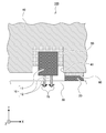
- FIG. 1 is a side view showing an electronic apparatus 1 using a heat dissipation structure according to the present invention.
- the electronic device 1 is different from the electronic device 100 according to the conventional example shown in FIG. 4 in that the first electronic component 10 ⁇ / b> A is provided instead of the first electronic component 10 and the heat sink 40 ⁇ / b> A is provided instead of the heat sink 40.
- the point which is equipped with the thermal radiation grease 50A instead of the thermal radiation grease 50, and the other part has the same form. For this reason, about the part which has the same form as the electronic device 100, the same code
- the first electronic component 10 ⁇ / b> A includes a main body 11 and two terminals 12 extending from one surface of the main body 11. These two terminals 12 are made of copper.
- the first electronic component 10 ⁇ / b> A is through-hole mounted on one surface (the surface on the Y minus direction side) of the electronic substrate 30.
- the first electronic component 10 ⁇ / b> A is provided on one surface side of the electronic substrate 30, and each of the two terminals 12 is an electron via each of two through holes provided in the electronic substrate 30. It protrudes to the other surface side of the substrate 30.
- a portion of the terminal 12 that protrudes to the other surface side of the electronic substrate 30 is fixed to the electronic substrate 30 by the solder portion 70.
- the solder portion 70 covers all portions of the terminal 12 that protrude to the other surface side of the electronic substrate 30. For this reason, the heat dissipation grease 50 ⁇ / b> A comes into contact with the portion of the terminal 12 that protrudes to the other surface side of the electronic substrate 30 via the solder portion 70.
- the heat sink 40 ⁇ / b> A as a heat radiating portion is provided on the other surface side of the electronic substrate 30 with a space between the electronic substrate 30.
- the recessed part 41 was formed in the heat sink 40 shown in FIG. 4, the main body 11 of the first electronic component 10A that affects the heat dissipation characteristics of the heat sink 40A is included in the heat sink 40A according to the present embodiment.
- the concave portion 41 that is inserted without being in contact with the wall portion is not formed.
- the heat dissipating grease 50A as the heat conducting portion is provided between the terminal 12 and the heat sink 40A.
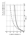
- FIG. 2 is a diagram illustrating a temperature change of the first electronic component 10A depending on the presence or absence of the heat dissipation grease 50A.
- the vertical axis indicates the temperature of the first electronic component 10A
- the horizontal axis indicates time.
- the temperature of the first electronic component 10A is raised to 100 ° C. by raising the temperature of the first electronic component 10A while the first electronic component 10A is not energized. This is the timing.
- the solid line graph shows the temperature change of the first electronic component 10 ⁇ / b> A when the heat dissipation grease 50 ⁇ / b> A is provided in the electronic device 1.
- the dashed-dotted line graph shows the temperature change of the first electronic component 10A when the electronic device 1 is not provided with the heat dissipation grease 50A.
- the temperature of the first electronic component 10A is about 7 degrees lower after 500 seconds than when the heat dissipation grease 50A is not provided.
- the first electronic component 10 ⁇ / b> A is mounted on one surface of the electronic substrate 30, and the heat sink 40 ⁇ / b> A is provided on the other surface of the electronic substrate 30.
- a heat radiation grease 50A is provided between a portion of the terminal 12 of the first electronic component 10A that protrudes to the other surface side of the electronic substrate 30 and the heat sink 40A. For this reason, the heat of the first electronic component 10A can be transmitted to the heat sink 40A via the terminal 12 and the heat dissipation grease 50A. For this reason, the recessed part 41 (refer FIG. 4) for inserting the main body 11 of 10 A of 1st electronic components becomes unnecessary.
- the heat radiation efficiency of the first electronic component 10A can be sufficiently improved.
- the first electronic component 10 ⁇ / b> A and the heat sink 40 ⁇ / b> A can be provided on different surfaces of the electronic substrate 30. Therefore, when the electronic component and the heat sink are provided on different sides of the electronic substrate 30 as in the present embodiment, and when provided on the same surface side of the electronic substrate 30 as shown in FIG. You can choose. Therefore, the degree of freedom in circuit design of a circuit including electronic components can be improved.
- the electronic device 1 causes the terminal 12 to protrude to the other surface side of the electronic substrate 30 through a through hole provided in the electronic substrate 30, and to the other surface side of the electronic substrate 30 among the terminals 12.
- the protruding part is covered with the solder part 70 so that the terminal 12 and the heat dissipation grease 50A are in contact with each other through the solder part 70. For this reason, the heat of the first electronic component 10A mounted with a so-called through hole can be transmitted to the heat sink 40A.
- the terminal 12 is made of copper. Since copper is a substance having high thermal conductivity, the heat radiation efficiency of the first electronic component 10A can be further improved.
- the terminal 12 is made of copper.
- the present invention is not limited to this, and the terminal 12 may be formed by covering a core material such as steel with copper.
- the solder portion 70 covers all the portions of the terminal 12 that protrude to the other surface side of the electronic substrate 30.
- a portion of the terminal 12 that protrudes toward the other surface of the electronic substrate 30 may be a portion that is not covered with the solder portion 70.
- the tip of the terminal 12 is cut to prevent the tip of the terminal 12 from being covered with solder or from being detached from the electronic substrate 30.
- only the tip of the terminal 12 may be soldered.
- the portion of the terminal 12 that protrudes to the other surface side of the electronic substrate 30 and is not covered by the solder portion 70 is directly connected to the heat dissipation grease 50 ⁇ / b> A without the solder portion 70 interposed therebetween. Will be in touch.
- FIG. 3 is a side view showing an electronic apparatus 1A using the heat dissipation structure according to the present invention.
- the electronic device 1A is different from the electronic device 1 according to the first embodiment of the present invention shown in FIG. 1 in that the electronic device 1A includes a first electronic component 10B instead of the first electronic component 10A, and penetrates the electronic substrate 30.
- the difference is that the hole 80 is formed, and the other parts have the same form. For this reason, about the part which has the same form as the electronic device 1, the same code
- the first electronic component 10B includes a main body 11A and a terminal 12A extending from one surface of the main body 11A.
- the terminal 12A is made of copper.
- the first electronic component 10B is surface-mounted on one surface (the surface on the Y minus direction side) of the electronic substrate 30.
- the first electronic component 10 ⁇ / b> B is provided on one surface side of the electronic substrate 30, and the terminal 12 abuts on one surface of the electronic substrate 30 and is fixed to the electronic substrate 30 by the solder portion 70.
- the through hole 80 is formed through the electronic substrate 30.
- a hole wall heat conducting portion 81 is provided on the hole wall of the through hole 80 so as to extend from one surface of the electronic substrate 30 to the other surface of the electronic substrate 30.
- the hole wall heat conduction part 81 has heat conductivity and is made of, for example, copper.
- the terminal 12 ⁇ / b> A is in contact with a portion on one surface side of the electronic substrate 30, and the heat radiation grease 50 ⁇ / b> A is in contact with a portion on the other surface side of the electronic substrate 30.
- the thermal radiation grease 50A which is in contact with the terminal 12A through the hole wall heat conduction part 81 is provided. Therefore, the heat of the first electronic component 10B can be transmitted to the heat sink 40A via the terminal 12A, the hole wall heat conducting portion 81, and the heat dissipation grease 50A. For this reason, the recessed part 41 (refer FIG. 4) for inserting the main body 11A of the 1st electronic component 10B becomes unnecessary. Therefore, since the volume of the heat sink 40A can be ensured, the heat radiation efficiency of the first electronic component 10B can be sufficiently improved.
- the first electronic component 10B and the heat sink 40A can be provided on different surfaces of the electronic substrate 30, respectively. Therefore, when the electronic component and the heat sink are provided on different sides of the electronic substrate 30 as in the present embodiment, and when provided on the same surface side of the electronic substrate 30 as shown in FIG. You can choose. Therefore, the degree of freedom in circuit design of a circuit including electronic components can be improved.
- the electronic device 1A causes the terminal 12A to contact one surface of the electronic substrate 30 and to contact the heat sink 40A via the hole wall heat conducting portion 81 and the heat radiation grease 50A. For this reason, the heat of the so-called surface-mounted first electronic component 10B can be transmitted to the heat sink 40A.
- the terminal 12A is made of copper. Since copper is a substance having a high thermal conductivity, the heat radiation efficiency of the first electronic component 10B can be further improved.
- the terminal 12A is made of copper.
- the present invention is not limited thereto, and the terminal 12A may be formed by covering a core material such as steel with copper.
Landscapes
- Engineering & Computer Science (AREA)
- Microelectronics & Electronic Packaging (AREA)
- Physics & Mathematics (AREA)
- Thermal Sciences (AREA)
- Cooling Or The Like Of Electrical Apparatus (AREA)
- Cooling Or The Like Of Semiconductors Or Solid State Devices (AREA)
Abstract
電子部品の熱の放熱効率を十分に向上させる放熱構造を提供する。 電子機器(1)は、電子基板(30)の一方の面に実装された第1の電子部品(10A)の熱を放熱する放熱構造を有する。この電子機器(1)は、ヒートシンク(40A)および放熱グリス(50A)を備える。ヒートシンク(40A)は、電子基板(30)の他方の面側に、電子基板(30)との間に間隔を空けて設けられる。放熱グリス(50A)は、第1の電子部品(10A)の端子(12)と、放熱グリス(50A)と、の間に設けられる。
Description
本発明は、放熱構造に関する。
電子基板に実装された電子部品は、電子部品の動作時に発熱することがある。そこで、電子部品の熱を放熱する放熱構造が提案されている(例えば、特許文献1参照)。
特許文献1には、電子基板の一方の面に電子部品を実装し、電子基板の他方の面に冷却器を当接させる放熱構造が示されている。この放熱構造では、電子部品の熱を、電子基板を介して冷却器に伝達させて、電子部品の熱を放熱させる。
上述のような電子部品の熱を放熱する放熱構造において、放熱効率の向上が求められている。そこで、例えば図4に示す電子機器100のように、電子部品の熱を、冷却器といった放熱部に、電子基板を介することなく伝達させる放熱構造が考えられる。
なお、以下に示す各図には、説明と理解を容易にするために、図中にXYZ直交座標系を設けたが、これらは単に図中の向きを統一して説明するために設定したものであり、絶対的な座標を示すものではない。
なお、以下に示す各図には、説明と理解を容易にするために、図中にXYZ直交座標系を設けたが、これらは単に図中の向きを統一して説明するために設定したものであり、絶対的な座標を示すものではない。
電子機器100は、第1の電子部品10、第2の電子部品20、電子基板30、ヒートシンク40、放熱グリス50、60、および半田部70を備える。
第1の電子部品10は、電子基板30の他方の面(Yプラス方向側の面)にスルーホール実装される。具体的には、第1の電子部品10は、電子基板30の他方の面側に設けられ、本体11と、本体11の一方の面から伸びる2つの端子12と、を備える。2つの端子12のそれぞれは、電子基板30に設けられた2つのスルーホールのそれぞれに挿通された状態で、半田部70により電子基板30に固着される。
一方、第2の電子部品20は、電子基板30の他方の面に表面実装される。
一方、第2の電子部品20は、電子基板30の他方の面に表面実装される。
ヒートシンク40は、電子基板30の他方の面側に、電子基板30との間に間隔を空けて設けられる。
ヒートシンク40には、凹部41が形成される。凹部41には、第1の電子部品10の本体11が、凹部41の壁部に当接しない状態で挿入される。凹部41の壁部と本体11との間には、放熱グリス50が設けられる。
また、ヒートシンク40と第2の電子部品20との間には、放熱グリス60が設けられる。
ヒートシンク40には、凹部41が形成される。凹部41には、第1の電子部品10の本体11が、凹部41の壁部に当接しない状態で挿入される。凹部41の壁部と本体11との間には、放熱グリス50が設けられる。
また、ヒートシンク40と第2の電子部品20との間には、放熱グリス60が設けられる。
以上の電子機器100では、第1の電子部品10の熱は、電子基板30を介してではなく、放熱グリス50を介してヒートシンク40に伝達される。また、第2の電子部品20の熱は、電子基板30を介してではなく、放熱グリス60を介してヒートシンク40に伝達される。
しかし、上述の電子機器100では、凹部41の体積分だけ、ヒートシンク40の体積が小さくなる。このため、第1の電子部品10の熱の放熱効率を十分には向上させることができないおそれがあった。
そこで、本発明は、上述の課題に鑑みてなされたものであり、電子部品の熱の放熱効率を十分に向上させる放熱構造を提供する。
本発明の1またはそれ以上の実施形態は、電子基板の一方の面に実装された電子部品の熱を放熱する放熱構造であって、前記電子基板の他方の面側に、前記電子基板との間に間隔を空けて設けられた放熱部と、前記電子部品の端子と前記放熱部との間に設けられた熱伝導部と、を備えることを特徴とする。
以下、本発明の実施の形態について図面を参照しながら説明する。なお、以下の実施形態における構成要素は適宜、既存の構成要素などとの置き換えが可能であり、また、他の既存の構成要素との組み合わせを含む様々なバリエーションが可能である。このため、以下の実施形態の記載をもって、特許請求の範囲に記載された発明の内容を限定するものではない。
<第1実施形態>
図1を用いて、本発明の第1実施形態について説明する。
図1を用いて、本発明の第1実施形態について説明する。
図1は、本発明による放熱構造を用いた電子機器1を示す側面図である。電子機器1は、図4に示した従来例に係る電子機器100とは、第1の電子部品10の代わりに第1の電子部品10Aを備える点と、ヒートシンク40の代わりにヒートシンク40Aを備える点と、放熱グリス50の代わりに放熱グリス50Aを備える点と、で異なっており、他の部分については同様の形態をしている。このため、電子機器100と同様の形態をしている部分については、同一の符号を付して、その説明を省略する。
第1の電子部品10Aは、第1の電子部品10と同様に、本体11と、本体11の一方の面から伸びる2つの端子12と、を備える。これら2つの端子12は、銅で構成される。
第1の電子部品10Aは、電子基板30の一方の面(Yマイナス方向側の面)にスルーホール実装される。具体的には、第1の電子部品10Aは、電子基板30の一方の面側に設けられ、2つの端子12のそれぞれは、電子基板30に設けられた2つのスルーホールのそれぞれを介して電子基板30の他方の面側に突出する。端子12のうち、電子基板30の他方の面側に突出している部分は、半田部70により電子基板30に固着される。
なお、本実施形態では、図1に示すように、半田部70は、端子12のうち、電子基板30の他方の面側に突出している部分を、全て覆っている。このため、放熱グリス50Aは、端子12のうち、電子基板30の他方の面側に突出している部分に、半田部70を介して接することになる。
第1の電子部品10Aは、電子基板30の一方の面(Yマイナス方向側の面)にスルーホール実装される。具体的には、第1の電子部品10Aは、電子基板30の一方の面側に設けられ、2つの端子12のそれぞれは、電子基板30に設けられた2つのスルーホールのそれぞれを介して電子基板30の他方の面側に突出する。端子12のうち、電子基板30の他方の面側に突出している部分は、半田部70により電子基板30に固着される。
なお、本実施形態では、図1に示すように、半田部70は、端子12のうち、電子基板30の他方の面側に突出している部分を、全て覆っている。このため、放熱グリス50Aは、端子12のうち、電子基板30の他方の面側に突出している部分に、半田部70を介して接することになる。
放熱部としてのヒートシンク40Aは、電子基板30の他方の面側に、電子基板30との間に間隔を空けて設けられる。なお、図4に示したヒートシンク40には、凹部41が形成されていたが、本実施形態に係るヒートシンク40Aには、ヒートシンク40Aの放熱特性に影響を与える第1の電子部品10Aの本体11が、その壁部に当接しない状態で挿入されるような凹部41は形成されない。
熱伝導部としての放熱グリス50Aは、端子12とヒートシンク40Aとの間に設けられる。
図2は、放熱グリス50Aの有無による第1の電子部品10Aの温度変化を示す図である。図2において、縦軸は、第1の電子部品10Aの温度を示し、横軸は、時間を示す。
また、図2において、時間0(ゼロ)は、第1の電子部品10Aに通電していない状態で第1の電子部品10Aの温度を上昇させて、第1の電子部品10Aの温度が100度になったタイミングである。
また、図2において、時間0(ゼロ)は、第1の電子部品10Aに通電していない状態で第1の電子部品10Aの温度を上昇させて、第1の電子部品10Aの温度が100度になったタイミングである。
実線のグラフは、電子機器1において、放熱グリス50Aを設けた場合における第1の電子部品10Aの温度変化を示している。一方、一点鎖線のグラフは、電子機器1において、放熱グリス50Aを設けなかった場合における第1の電子部品10Aの温度変化を示している。
図2では、放熱グリス50Aを設けた場合、放熱グリス50Aを設けなかった場合と比べて、第1の電子部品10Aの温度が500sec後には、約7度低くなっている。
図2では、放熱グリス50Aを設けた場合、放熱グリス50Aを設けなかった場合と比べて、第1の電子部品10Aの温度が500sec後には、約7度低くなっている。
以上のように、電子機器1は、電子基板30の一方の面に第1の電子部品10Aを実装し、電子基板30の他方の面にヒートシンク40Aを設ける。また、第1の電子部品10Aの端子12のうち電子基板30の他方の面側に突出している部分と、ヒートシンク40Aと、の間に放熱グリス50Aを設ける。このため、第1の電子部品10Aの熱を、端子12および放熱グリス50Aを介してヒートシンク40Aに伝達することができる。
このため、第1の電子部品10Aの本体11を挿入するための凹部41(図4参照)が不要になる。したがって、ヒートシンク40Aの体積を確保することができるので、第1の電子部品10Aの熱の放熱効率を十分に向上させることができる。
また、第1の電子部品10Aとヒートシンク40Aとを、それぞれ電子基板30の異なる面側に設けることができる。このため、電子部品とヒートシンクとを、本実施形態のようにそれぞれ電子基板30の異なる面側に設ける場合と、図4に示したように電子基板30の同一の面側に設ける場合と、を選択することができる。したがって、電子部品を含む回路の回路設計の自由度を、向上させることもできる。
このため、第1の電子部品10Aの本体11を挿入するための凹部41(図4参照)が不要になる。したがって、ヒートシンク40Aの体積を確保することができるので、第1の電子部品10Aの熱の放熱効率を十分に向上させることができる。
また、第1の電子部品10Aとヒートシンク40Aとを、それぞれ電子基板30の異なる面側に設けることができる。このため、電子部品とヒートシンクとを、本実施形態のようにそれぞれ電子基板30の異なる面側に設ける場合と、図4に示したように電子基板30の同一の面側に設ける場合と、を選択することができる。したがって、電子部品を含む回路の回路設計の自由度を、向上させることもできる。
また、電子機器1は、端子12を、電子基板30に設けられたスルーホールを介して、電子基板30の他方の面側に突出させ、端子12のうち、電子基板30の他方の面側に突出している部分を、半田部70により覆って、半田部70を介して端子12と放熱グリス50Aとが接するようにする。このため、いわゆるスルーホール実装された第1の電子部品10Aの熱を、ヒートシンク40Aに伝達することができる。
また、電子機器1は、端子12を銅で構成した。銅は、熱伝導率の高い物質であるため、第1の電子部品10Aの熱の放熱効率をさらに向上させることができる。
なお、本実施形態では、端子12を、銅で構成した。しかし、これに限らず、端子12を、例えば鋼といった芯材を、銅で覆って形成してもよい。
また、本実施形態では、半田部70により、端子12のうち、電子基板30の他方の面側に突出している部分を、全て覆った。しかし、これに限らず、端子12のうち、電子基板30の他方の面側に突出している部分に、半田部70で覆われていない部分があってもよい。具体例としては、端子12に半田付けを行った後に、端子12の先端部をカットすることにより、端子12の先端部が半田に覆われていない場合や電子基板30からの離脱を防止するために、端子12の折り曲げ処理を行なった後に、端子12の先端部のみに半田付けを行なう場合がある。上記の例示では、端子12のうち、電子基板30の他方の面側に突出している部分であって、半田部70に覆われていない部分は、半田部70を介することなく放熱グリス50Aに直接接することになる。
<第2実施形態>
図3を用いて、本発明の第2実施形態について説明する。
図3を用いて、本発明の第2実施形態について説明する。
図3は、本発明による放熱構造を用いた電子機器1Aを示す側面図である。電子機器1Aは、図1に示した本発明の第1実施形態に係る電子機器1とは、第1の電子部品10Aの代わりに第1の電子部品10Bを備える点と、電子基板30に貫通孔80が形成されている点と、で異なっており、他の部分については同様の形態をしている。このため、電子機器1と同様の形態をしている部分については、同一の符号を付して、その説明を省略する。
第1の電子部品10Bは、本体11Aと、本体11Aの一方の面から伸びる端子12Aと、を備える。端子12Aは、銅で構成される。
第1の電子部品10Bは、電子基板30の一方の面(Yマイナス方向側の面)に表面実装される。具体的には、第1の電子部品10Bは、電子基板30の一方の面側に設けられ、端子12は、電子基板30の一方の面に当接し、半田部70により電子基板30に固着される。
第1の電子部品10Bは、電子基板30の一方の面(Yマイナス方向側の面)に表面実装される。具体的には、第1の電子部品10Bは、電子基板30の一方の面側に設けられ、端子12は、電子基板30の一方の面に当接し、半田部70により電子基板30に固着される。
貫通孔80は、電子基板30を貫通して形成される。貫通孔80の孔壁には、孔壁熱伝導部81が、電子基板30の一方の面から電子基板30の他方の面まで延在して設けられる。孔壁熱伝導部81は、熱伝導性を有しており、例えば銅で構成される。
孔壁熱伝導部81のうち、電子基板30の一方の面側の部分には端子12Aが接し、電子基板30の他方の面側の部分には放熱グリス50Aが接する。
以上のように、電子機器1Aは、電子基板30の一方の面に第1の電子部品10Bを実装し、電子基板30の他方の面にヒートシンク40Aを設ける。また、電子基板30に貫通孔80を形成し、貫通孔80の孔壁に、熱伝導性を有する孔壁熱伝導部81を、電子基板30の一方の面から電子基板30の他方の面まで延在して設ける。また、端子12Aは、孔壁熱伝導部81のうち、電子基板30の一方の面側の部分に接し、放熱グリス50Aは、孔壁熱伝導部81のうち、電子基板30の他方の面側の部分に接する。このため、第1の電子部品10Bの端子12Aと、ヒートシンク40Aと、の間には、孔壁熱伝導部81を介して端子12Aに接している放熱グリス50Aが設けられる。したがって、第1の電子部品10Bの熱を、端子12A、孔壁熱伝導部81、および放熱グリス50Aを介してヒートシンク40Aに伝達することができる。
このため、第1の電子部品10Bの本体11Aを挿入するための凹部41(図4参照)が不要になる。したがって、ヒートシンク40Aの体積を確保することができるので、第1の電子部品10Bの熱の放熱効率を十分に向上させることができる。
また、第1の電子部品10Bとヒートシンク40Aとを、それぞれ電子基板30の異なる面側に設けることができる。このため、電子部品とヒートシンクとを、本実施形態のようにそれぞれ電子基板30の異なる面側に設ける場合と、図4に示したように電子基板30の同一の面側に設ける場合と、を選択することができる。したがって、電子部品を含む回路の回路設計の自由度を、向上させることもできる。
このため、第1の電子部品10Bの本体11Aを挿入するための凹部41(図4参照)が不要になる。したがって、ヒートシンク40Aの体積を確保することができるので、第1の電子部品10Bの熱の放熱効率を十分に向上させることができる。
また、第1の電子部品10Bとヒートシンク40Aとを、それぞれ電子基板30の異なる面側に設けることができる。このため、電子部品とヒートシンクとを、本実施形態のようにそれぞれ電子基板30の異なる面側に設ける場合と、図4に示したように電子基板30の同一の面側に設ける場合と、を選択することができる。したがって、電子部品を含む回路の回路設計の自由度を、向上させることもできる。
また、電子機器1Aは、端子12Aを、電子基板30の一方の面に当接させるとともに、孔壁熱伝導部81および放熱グリス50Aを介してヒートシンク40Aに接するようにする。このため、いわゆる表面実装された第1の電子部品10Bの熱を、ヒートシンク40Aに伝達することができる。
また、電子機器1Aは、端子12Aを銅で構成した。銅は、熱伝導率の高い物質であるため、第1の電子部品10Bの熱の放熱効率をさらに向上させることができる。
なお、本実施形態では、端子12Aを、銅で構成した。しかし、これに限らず、端子12Aを、例えば鋼といった芯材を、銅で覆って形成してもよい。
以上、第1の実施形態及び第2の実施形態について説明したが、これらの実施形態によれば、電子部品の熱の放熱効率を十分に向上させることができるという効果がある。
なお、この発明の実施形態につき、図面を参照して詳述してきたが、具体的な構成はこの実施形態に限られるものではなく、この発明の要旨を逸脱しない範囲の設計なども含まれる。
1、1A、100 電子機器
10、10A、10B 第1の電子部品
11、11A 本体
12、12A 端子
20 第2の電子部品
30 電子基板
40、40A ヒートシンク(放熱部)
41 凹部
50、50A、60 放熱グリス(熱伝導部)
70 半田部
80 貫通孔
81 孔壁熱伝導部
10、10A、10B 第1の電子部品
11、11A 本体
12、12A 端子
20 第2の電子部品
30 電子基板
40、40A ヒートシンク(放熱部)
41 凹部
50、50A、60 放熱グリス(熱伝導部)
70 半田部
80 貫通孔
81 孔壁熱伝導部
Claims (5)
- 電子基板の一方の面に実装された電子部品の熱を放熱する放熱構造であって、
前記電子基板の他方の面側に、前記電子基板との間に間隔を空けて設けられた放熱部と、
前記電子部品の端子と前記放熱部との間に設けられた熱伝導部と、を備えることを特徴とする放熱構造。 - 前記電子基板には、前記電子基板を貫通する貫通孔が設けられ、
前記電子部品の端子は、前記貫通孔を介して前記電子基板の他方の面側に突出し、
前記熱伝導部は、前記電子部品の端子のうち、前記電子基板の他方の面側に突出している部分に接することを特徴とする請求項1に記載の放熱構造。 - 前記電子部品の端子のうち、前記電子基板の他方の面側に突出している部分は、半田部により前記電子基板に固着され、
前記熱伝導部は、前記半田部を介して前記電子部品の端子に接することを特徴とする請求項2に記載の放熱構造。 - 前記電子基板には、前記電子基板を貫通する貫通孔が設けられ、
前記貫通孔の孔壁には、熱伝導性を有する孔壁熱伝導部が、前記電子基板の一方の面から前記電子基板の他方の面まで延在して設けられ、
前記電子部品の端子は、前記孔壁熱伝導部のうち、前記電子基板の一方の面側の部分に接し、
前記熱伝導部は、前記孔壁熱伝導部のうち、前記電子基板の他方の面側の部分に接することを特徴とする請求項1に記載の放熱構造。 - 前記電子部品の端子は、銅で覆われているか、または銅で構成されていることを特徴とする請求項1に記載の放熱構造。
Applications Claiming Priority (2)
| Application Number | Priority Date | Filing Date | Title |
|---|---|---|---|
| JP2016-143264 | 2016-07-21 | ||
| JP2016143264A JP2018014415A (ja) | 2016-07-21 | 2016-07-21 | 放熱構造 |
Publications (1)
| Publication Number | Publication Date |
|---|---|
| WO2018016144A1 true WO2018016144A1 (ja) | 2018-01-25 |
Family
ID=60993289
Family Applications (1)
| Application Number | Title | Priority Date | Filing Date |
|---|---|---|---|
| PCT/JP2017/015568 Ceased WO2018016144A1 (ja) | 2016-07-21 | 2017-04-18 | 放熱構造 |
Country Status (2)
| Country | Link |
|---|---|
| JP (1) | JP2018014415A (ja) |
| WO (1) | WO2018016144A1 (ja) |
Families Citing this family (3)
| Publication number | Priority date | Publication date | Assignee | Title |
|---|---|---|---|---|
| KR102937316B1 (ko) * | 2019-11-13 | 2026-03-10 | 엘지이노텍 주식회사 | 컨버터 |
| JP7208550B2 (ja) | 2021-03-30 | 2023-01-19 | ダイキン工業株式会社 | 電装品および冷凍装置 |
| CN119866419A (zh) * | 2022-09-27 | 2025-04-22 | 三菱电机株式会社 | 驱动装置以及空调装置 |
Citations (5)
| Publication number | Priority date | Publication date | Assignee | Title |
|---|---|---|---|---|
| JPH03128965U (ja) * | 1990-04-11 | 1991-12-25 | ||
| JP2001068607A (ja) * | 1999-08-31 | 2001-03-16 | Hitachi Ltd | 電子部品の冷却構造 |
| US7176707B1 (en) * | 2006-02-23 | 2007-02-13 | Lockheed Martin Corporation | Back side component placement and bonding |
| JP2008205356A (ja) * | 2007-02-22 | 2008-09-04 | Siix Corp | 回路基板及び回路基板への電子部品実装方法 |
| WO2015076050A1 (ja) * | 2013-11-20 | 2015-05-28 | 日立オートモティブシステムズ株式会社 | 電子制御装置の実装構造 |
-
2016
- 2016-07-21 JP JP2016143264A patent/JP2018014415A/ja active Pending
-
2017
- 2017-04-18 WO PCT/JP2017/015568 patent/WO2018016144A1/ja not_active Ceased
Patent Citations (5)
| Publication number | Priority date | Publication date | Assignee | Title |
|---|---|---|---|---|
| JPH03128965U (ja) * | 1990-04-11 | 1991-12-25 | ||
| JP2001068607A (ja) * | 1999-08-31 | 2001-03-16 | Hitachi Ltd | 電子部品の冷却構造 |
| US7176707B1 (en) * | 2006-02-23 | 2007-02-13 | Lockheed Martin Corporation | Back side component placement and bonding |
| JP2008205356A (ja) * | 2007-02-22 | 2008-09-04 | Siix Corp | 回路基板及び回路基板への電子部品実装方法 |
| WO2015076050A1 (ja) * | 2013-11-20 | 2015-05-28 | 日立オートモティブシステムズ株式会社 | 電子制御装置の実装構造 |
Also Published As
| Publication number | Publication date |
|---|---|
| JP2018014415A (ja) | 2018-01-25 |
Similar Documents
| Publication | Publication Date | Title |
|---|---|---|
| JP6129177B2 (ja) | 電子部品モジュールとその実装体 | |
| JPWO2017017885A1 (ja) | 実装構造体、実装構造体の製造方法、無線機 | |
| WO2018038030A1 (ja) | 導電部材、回路構成体、及び、導電部材の製造方法 | |
| JP6330690B2 (ja) | 基板ユニット | |
| WO2018016144A1 (ja) | 放熱構造 | |
| CN105744724A (zh) | 电子器件的散热结构、穿戴式电子设备及其散热方法 | |
| US10674596B2 (en) | Electronic component, electronic component manufacturing method, and mechanical component | |
| JP2015142108A (ja) | 放熱板及び半導体装置 | |
| JP2016051751A (ja) | 半導体装置 | |
| CN205726813U (zh) | 一种电子设备 | |
| JP5791344B2 (ja) | 撮像素子搭載用部材および撮像装置 | |
| JP3176322U (ja) | 多層プリント基板の放熱構造 | |
| JP2009253116A (ja) | スペーサの構造 | |
| JP2006041199A (ja) | 電子装置 | |
| JP6543226B2 (ja) | 電子装置 | |
| WO2015098503A1 (ja) | 電子部品 | |
| JP2005166981A (ja) | 電子制御装置 | |
| TWI504325B (zh) | Three-dimensional circuit board | |
| JP5611724B2 (ja) | 回路基板装置 | |
| JP2007149914A (ja) | 電子部品の実装方法 | |
| WO2018029909A1 (ja) | 放熱構造 | |
| CN204272478U (zh) | 一种新型pcb板 | |
| KR101168068B1 (ko) | 금속기판 접속구조물, 이를 구비한 엘이디 모듈 및 금속기판 접속방법 | |
| JP2006308618A (ja) | 絶縁放熱板 | |
| JP2005158830A (ja) | 終端抵抗の放熱取付構造 |
Legal Events
| Date | Code | Title | Description |
|---|---|---|---|
| DPE1 | Request for preliminary examination filed after expiration of 19th month from priority date (pct application filed from 20040101) | ||
| 121 | Ep: the epo has been informed by wipo that ep was designated in this application |
Ref document number: 17830664 Country of ref document: EP Kind code of ref document: A1 |
|
| NENP | Non-entry into the national phase |
Ref country code: DE |
|
| 122 | Ep: pct application non-entry in european phase |
Ref document number: 17830664 Country of ref document: EP Kind code of ref document: A1 |