WO2018003590A1 - Heat-curable resin composition, resin film with carrier, printed wiring board, and semiconductor device - Google Patents
Heat-curable resin composition, resin film with carrier, printed wiring board, and semiconductor device Download PDFInfo
- Publication number
- WO2018003590A1 WO2018003590A1 PCT/JP2017/022627 JP2017022627W WO2018003590A1 WO 2018003590 A1 WO2018003590 A1 WO 2018003590A1 JP 2017022627 W JP2017022627 W JP 2017022627W WO 2018003590 A1 WO2018003590 A1 WO 2018003590A1
- Authority
- WO
- WIPO (PCT)
- Prior art keywords
- resin composition
- thermosetting resin
- wiring board
- printed wiring
- resin
- Prior art date
Links
Images


Classifications
-
- B—PERFORMING OPERATIONS; TRANSPORTING
- B32—LAYERED PRODUCTS
- B32B—LAYERED PRODUCTS, i.e. PRODUCTS BUILT-UP OF STRATA OF FLAT OR NON-FLAT, e.g. CELLULAR OR HONEYCOMB, FORM
- B32B27/00—Layered products comprising a layer of synthetic resin
- B32B27/18—Layered products comprising a layer of synthetic resin characterised by the use of special additives
- B32B27/20—Layered products comprising a layer of synthetic resin characterised by the use of special additives using fillers, pigments, thixotroping agents
-
- B—PERFORMING OPERATIONS; TRANSPORTING
- B32—LAYERED PRODUCTS
- B32B—LAYERED PRODUCTS, i.e. PRODUCTS BUILT-UP OF STRATA OF FLAT OR NON-FLAT, e.g. CELLULAR OR HONEYCOMB, FORM
- B32B27/00—Layered products comprising a layer of synthetic resin
- B32B27/38—Layered products comprising a layer of synthetic resin comprising epoxy resins
-
- C—CHEMISTRY; METALLURGY
- C08—ORGANIC MACROMOLECULAR COMPOUNDS; THEIR PREPARATION OR CHEMICAL WORKING-UP; COMPOSITIONS BASED THEREON
- C08K—Use of inorganic or non-macromolecular organic substances as compounding ingredients
- C08K3/00—Use of inorganic substances as compounding ingredients
- C08K3/34—Silicon-containing compounds
- C08K3/36—Silica
-
- C—CHEMISTRY; METALLURGY
- C08—ORGANIC MACROMOLECULAR COMPOUNDS; THEIR PREPARATION OR CHEMICAL WORKING-UP; COMPOSITIONS BASED THEREON
- C08L—COMPOSITIONS OF MACROMOLECULAR COMPOUNDS
- C08L101/00—Compositions of unspecified macromolecular compounds
-
- C—CHEMISTRY; METALLURGY
- C08—ORGANIC MACROMOLECULAR COMPOUNDS; THEIR PREPARATION OR CHEMICAL WORKING-UP; COMPOSITIONS BASED THEREON
- C08L—COMPOSITIONS OF MACROMOLECULAR COMPOUNDS
- C08L63/00—Compositions of epoxy resins; Compositions of derivatives of epoxy resins
-
- C—CHEMISTRY; METALLURGY
- C08—ORGANIC MACROMOLECULAR COMPOUNDS; THEIR PREPARATION OR CHEMICAL WORKING-UP; COMPOSITIONS BASED THEREON
- C08L—COMPOSITIONS OF MACROMOLECULAR COMPOUNDS
- C08L71/00—Compositions of polyethers obtained by reactions forming an ether link in the main chain; Compositions of derivatives of such polymers
-
- H—ELECTRICITY
- H05—ELECTRIC TECHNIQUES NOT OTHERWISE PROVIDED FOR
- H05K—PRINTED CIRCUITS; CASINGS OR CONSTRUCTIONAL DETAILS OF ELECTRIC APPARATUS; MANUFACTURE OF ASSEMBLAGES OF ELECTRICAL COMPONENTS
- H05K1/00—Printed circuits
- H05K1/02—Details
- H05K1/03—Use of materials for the substrate
-
- C—CHEMISTRY; METALLURGY
- C08—ORGANIC MACROMOLECULAR COMPOUNDS; THEIR PREPARATION OR CHEMICAL WORKING-UP; COMPOSITIONS BASED THEREON
- C08J—WORKING-UP; GENERAL PROCESSES OF COMPOUNDING; AFTER-TREATMENT NOT COVERED BY SUBCLASSES C08B, C08C, C08F, C08G or C08H
- C08J3/00—Processes of treating or compounding macromolecular substances
- C08J3/24—Crosslinking, e.g. vulcanising, of macromolecules
Definitions
- the present invention relates to a thermosetting resin composition, a resin film with a carrier, a printed wiring board, and a semiconductor device.
- epoxy resin compositions have been developed in various ways from the viewpoint of reducing dimensional changes.
- an epoxy resin composition described in Patent Document 1 can be cited.
- the epoxy resin of this epoxy resin composition a bisphenol F type epoxy resin is used (paragraph 0124 of Patent Document 1, Example 2).
- the present inventor further examined the thermosetting resin composition used for forming the insulating layer in the printed wiring board, and focused on the elastic modulus and the elongation as characteristics related to toughness. As a result of further investigation, it has been found that excellent toughness can be realized by achieving both low elasticity and high elongation. And, by adopting the storage elastic modulus E ′ 30 at 30 ° C. as the elastic modulus index, and adopting the tensile elongation measured by the tensile test as the elongation index, low elasticity and high elongation are obtained. It has been found that it can be evaluated optimally.
- the storage modulus E '30 of the cured product of the thermosetting resin composition is less than a predetermined value, and, by a tensile elongation greater than or equal to a predetermined value, heat It has been found that the toughness of the cured product of the curable resin composition can be improved, and the present invention has been completed.
- thermosetting resin composition used for forming an insulating layer in a printed wiring board A thermosetting resin; A curing agent; An inorganic filler,
- the storage elastic modulus E ′ 30 at 30 ° C. of the cured product is 1 GPa or more and 10 GPa or less
- a thermosetting resin composition having a tensile elongation of 2% or more is provided.
- a carrier substrate There is provided a resin film with a carrier comprising: a resin film formed of the thermosetting resin composition provided on the carrier substrate.
- a printed wiring board provided with an insulating layer composed of a cured product of a resin film of the thermosetting resin composition is provided.
- the printed wiring board There is provided a semiconductor device comprising a semiconductor element mounted on a circuit layer of the printed wiring board or built in the printed wiring board.
- thermosetting resin from which an insulating layer having excellent toughness can be obtained a resin film with a carrier using the same, a printed wiring board, and a semiconductor device are provided.
- FIG. 1 is a cross-sectional view showing an example of the configuration of the resin film with a carrier in the present embodiment.
- 2A and 2B are cross-sectional views showing an example of the configuration of the printed wiring board in the present embodiment.
- 3A and 3B are cross-sectional views showing an example of the configuration of the semiconductor device in the present embodiment.
- 4A to 4C are process cross-sectional views illustrating an example of the manufacturing process of the printed wiring board in the present embodiment.
- FIG. 5 is a cross-sectional view showing an example of the configuration of the printed wiring board in the present embodiment.
- FIG. 6 is a cross-sectional view showing an example of the configuration of the printed wiring board in the present embodiment.
- the thermosetting resin composition of the present embodiment includes a thermosetting resin, a curing agent, and an inorganic filler. Moreover, when the thermosetting resin composition of this embodiment performs dynamic viscoelasticity measurement with respect to the hardened
- a thermosetting resin composition is used for forming an insulating layer in a printed wiring board.
- thermosetting resin composition used for forming an insulating layer in a printed wiring board, and has come to focus on storage elastic modulus and tensile elongation as characteristics relating to toughness.
- a thermosetting resin composition containing a thermosetting resin, a curing agent, and an inorganic filler, it is excellent in achieving both low elasticity and high elongation. It has been found that toughness can be exhibited.
- thermosetting resin having a large molecular weight per number of functional groups and a flexible skeleton, etc., controls the crosslink density and makes the storage elastic modulus and the tensile elongation rate within a desired numerical range.
- thermosetting resin composition As a result of intensive studies based on such knowledge, by setting the storage elastic modulus E ′ 30 of the cured product of the thermosetting resin composition to 1 GPa or more and 10 GPa or less and the tensile elongation rate to 2% or more, The present inventors have found that the low elasticity and high elongation of the cured product of the thermosetting resin composition can be compatible and can exhibit excellent toughness, and the present invention has been completed.
- the insulating layer in the printed wiring board can be used as an insulating member constituting the printed wiring board such as a core layer, a build-up layer (interlayer insulating layer), a solder resist layer, and the like.
- the printed wiring board includes a core layer, a build-up layer (interlayer insulating layer), a printed wiring board having a solder resist layer, a printed wiring board having no core layer, a coreless board used for a panel package process (PLP), MIS (Molded Interconnect Substrate) substrate and the like.
- the cured product of the resin film formed with the thermosetting resin composition of this embodiment is used for the insulating layer, for example, a build-up layer, a solder resist layer, or a PLP in a printed wiring board that does not have a core layer. It can also be used for an interlayer insulating layer and a solder resist layer of a coreless substrate, an interlayer insulating layer and a solder resist layer of a MIS substrate, and the like.
- the cured product of the resin film according to the present embodiment is a large-area printed wiring board used to collectively create a plurality of semiconductor packages. It can also be suitably used for the resist layer.
- the cured resin film of this embodiment As an insulating layer, it has excellent toughness. Therefore, during panel level processes for manufacturing large panel size packages, panel (coreless substrate) warpage and during transport And substrate cracks during mounting can be suppressed.
- the cured product of the resin film of the present embodiment it becomes possible to highly fill the inorganic filler in the matrix resin having a flexible skeleton.
- cured material of the said resin film can be made low, the curvature of the semiconductor package obtained can fully be suppressed.
- thermosetting resin composition of the present embodiment Each component of the thermosetting resin composition of the present embodiment will be described.
- thermosetting resin composition of the present embodiment includes, for example, a thermosetting resin, a curing agent, and an inorganic filler.
- thermosetting resin As a thermosetting resin, an epoxy resin, a maleimide compound, etc. are mentioned, for example. These may be used alone or in combination of two or more.
- the thermosetting resin preferably contains at least an epoxy resin or a maleimide compound, and particularly preferably contains an epoxy resin.
- thermosetting resin of the present embodiment is preferably liquid at 25 ° C. room temperature. Thereby, the dispersibility of each component in a thermosetting resin composition can be improved. Moreover, it becomes possible to raise the filling amount of an inorganic filler.
- the lower limit of the viscosity at 25 ° C. of the thermosetting resin of this embodiment is, for example, 0.1 Pa ⁇ s or more, preferably 0.5 Pa ⁇ s or more, and preferably 1 Pa ⁇ s or more. More preferred. Thereby, the film-forming property of a thermosetting resin composition can be improved.
- the upper limit of the viscosity at 25 ° C. is, for example, 200 Pa ⁇ s or less, preferably 100 Pa ⁇ s or less, and more preferably 50 Pa ⁇ s or less. Thereby, the dispersibility of a thermosetting resin composition can be improved.
- the lower limit of the epoxy equivalent of the epoxy resin of the present embodiment is, for example, 300 g / eq or more, preferably 330 g / eq or more, and more preferably 350 g / eq or more.
- the upper limit value of the epoxy equivalent is not particularly limited, but is, for example, 700 g / eq or less, preferably 600 g / eq or less, and more preferably 500 g / eq or less.
- cured material of a thermosetting resin composition can be improved.
- the lower limit of the weight average molecular weight (Mw) of the epoxy resin of the present embodiment is not particularly limited, but is preferably Mw 300 or more, and more preferably Mw 800 or more. It can suppress that a tack
- the upper limit of Mw is not particularly limited, but is preferably Mw 20,000 or less, and more preferably Mw 15,000 or less. When Mw is not more than the above upper limit value, the handling property is improved and it becomes easy to form a resin film.
- the Mw of the epoxy resin can be measured by GPC, for example.
- the epoxy resin of this embodiment is preferably liquid at 25 ° C. room temperature, and preferably contains at least one first epoxy resin having an epoxy equivalent in the above range.
- the type of the first epoxy resin is not particularly limited, but for example, bisphenol A type epoxy resin, bisphenol F type epoxy resin, bisphenol E type epoxy resin, bisphenol S type epoxy resin, bisphenol M type epoxy resin, bisphenol P type epoxy Resin, bisphenol type epoxy resin such as bisphenol Z type epoxy resin; phenol novolak type epoxy resin, cresol novolak type epoxy resin, tetraphenol group ethane type novolak type epoxy resin, novolak type epoxy resin having condensed ring aromatic hydrocarbon structure, etc.
- Novolac-type epoxy resins biphenyl-type epoxy resins; aralkyl-type epoxy resins such as xylylene-type epoxy resins and biphenyl-aralkyl-type epoxy resins; naphthylene ether-type resins Naphthalene-type epoxy resins such as xylene resin, naphthol-type epoxy resin, naphthalenediol-type epoxy resin, bifunctional to tetrafunctional naphthalene-type epoxy resin, binaphthyl-type epoxy resin, naphthalene-aralkyl-type epoxy resin; anthracene-type epoxy resin; phenoxy-type epoxy resin Dicyclopentadiene type epoxy resin; norbornene type epoxy resin; adamantane type epoxy resin; fluorene type epoxy resin; polyether type epoxy resin.
- aralkyl-type epoxy resins such as xylylene-type epoxy resins and biphenyl-aralkyl-type epoxy resins
- the first epoxy resins from the viewpoint of viscosity, at least one selected from bisphenol A type epoxy resins, fluorene type epoxy resins, bifunctional naphthalene type epoxy resins, and polyether type epoxy resins can be used.
- the epoxy resin of the present embodiment in addition to the first epoxy resin, another second epoxy resin may be used in combination.
- the second epoxy resin can be selected from the types of epoxy resins mentioned as the first epoxy resin.
- epoxy resins bisphenol type epoxy resin, novolac type epoxy resin, biphenyl type epoxy resin, aralkyl type epoxy resin, naphthalene type from the viewpoint of further improving the heat resistance and insulation reliability of the obtained printed wiring board It is preferable to use one or more selected from an epoxy resin, an anthracene type epoxy resin, and a dicyclopentadiene type epoxy resin. It is more preferable to use one or more selected from aralkyl type epoxy resins, novolak type epoxy resins having a condensed ring aromatic hydrocarbon structure, and naphthalene type epoxy resins.
- the lower limit of the content of the epoxy resin is preferably 3% by weight or more, more preferably 4% by weight or more, more preferably 5% by weight with respect to 100% by weight of the entire thermosetting resin composition (total solid content excluding the solvent). The above is more preferable.
- the upper limit of the content of the epoxy resin is not particularly limited with respect to the entire thermosetting resin composition, but is preferably 60% by weight or less, more preferably 45% by weight or less, and more preferably 30% by weight or less. Further preferred.
- thermosetting resin composition refers to the whole component except the solvent contained in a thermosetting resin composition. The same applies hereinafter.
- the thermosetting resin composition of this embodiment can contain a maleimide compound.
- the maleimide group of the maleimide compound has a five-membered planar structure.
- the double bond of the maleimide group is easy to interact between molecules and has high polarity. Therefore, a strong intermolecular interaction is exhibited with a maleimide group, a benzene ring, other compounds having a planar structure, and the like, and molecular motion can be suppressed. Therefore, when the thermosetting resin composition contains a maleimide compound, the linear expansion coefficient of the obtained insulating layer can be lowered, the glass transition temperature can be improved, and the heat resistance can be further improved.
- the maleimide compound is preferably a maleimide compound having at least two maleimide groups in the molecule.
- the imide-expanded bismaleimide include a maleimide compound represented by the following formula (a1), a maleimide compound represented by the following formula (a2), a maleimide compound represented by the following formula (a3), and the like.
- Specific examples of the maleimide compound represented by the formula (a1) include BMI-1500 (manufactured by Designa Molecules Co., Ltd., molecular weight 1500).
- maleimide compound represented by the formula (a2) examples include BMI-1700 (manufactured by Designer Molecules, molecular weight 1700), BMI-1400 (manufactured by Diginer Molecules, molecular weight 1400), and the like.
- Specific examples of the maleimide compound represented by the formula (a3) include BMI-3000 (manufactured by Designa Molecules Co., Ltd., molecular weight 3000).
- n represents an integer of 1 or more and 10 or less.
- n represents an integer of 1 or more and 10 or less.
- n represents an integer of 1 or more and 10 or less.
- the lower limit of the weight average molecular weight (Mw) of the maleimide compound is not particularly limited, but is preferably Mw 400 or more, and particularly preferably Mw 800 or more. When Mw is equal to or greater than the lower limit, it is possible to suppress the occurrence of tack in the insulating layer.
- the upper limit of Mw is not specifically limited, Mw4000 or less is preferable and Mw2500 or less is more preferable. When Mw is not more than the above upper limit value, handling properties are improved during the production of the insulating layer, and it becomes easy to form the insulating layer.
- the Mw of the maleimide compound can be measured, for example, by GPC (gel permeation chromatography, standard substance: converted to polystyrene).
- the Mw of the imide-extended bismaleimide having maleimide at both ends can be regarded as the molecular weight between crosslinking points.
- the content of the maleimide compound contained in the thermosetting resin composition is not particularly limited, but the total solid content of the thermosetting resin composition (that is, the component excluding the solvent) is 100% by weight. 1.0 wt% or more and 25.0 wt% or less is preferable, and 3.0 wt% or more and 20.0 wt% or less is more preferable.
- the content of the maleimide compound is within the above range, the balance of low heat shrinkage and chemical resistance of the obtained insulating layer can be further improved.
- thermosetting resin composition of this embodiment may contain a benzoxazine compound.
- a benzoxazine compound is a compound having a benzoxazine ring.
- the benzoxazine compound for example, one or more selected from a compound represented by the following formula (2) and a compound represented by the following formula (3) can be used.
- each X 2 independently represents an alkylene group having 1 to 10 carbon atoms, a group represented by the following formula (1a), a group represented by “—SO 2 —”, “—CO A group represented by “—”, an oxygen atom or a single bond, R 2 is each independently a hydrocarbon group having 1 to 6 carbon atoms, and c is each independently an integer of 0 to 4).
- X 3 each independently represents an alkylene group having 1 to 10 carbon atoms, a group represented by the following formula (1a), a group represented by “—SO 2 —”, “—CO A group represented by “—”, an oxygen atom or a single bond, R 3 is each independently a hydrocarbon group having 1 to 6 carbon atoms, and d is each independently an integer of 0 to 4).
- Y is a hydrocarbon group having 6 to 30 carbon atoms having an aromatic ring, and n 2 is an integer of 0 or more.
- the hydrocarbon group having 6 to 30 carbon atoms having an aromatic ring may be composed only of an aromatic ring, or may have a hydrocarbon group other than the aromatic ring.
- Y may have one aromatic ring or two or more aromatic rings. When Y has two or more aromatic rings, these aromatic rings may be the same or different.
- the aromatic ring may be a monocyclic structure or a polycyclic structure.
- Examples of the hydrocarbon group having 6 to 30 carbon atoms having an aromatic ring include aromatic compounds such as benzene, biphenyl, naphthalene, anthracene, fluorene, phenanthrene, indacene, terphenyl, acenaphthylene, and phenalene.
- these aromatic hydrocarbon groups may have a substituent.
- that the aromatic hydrocarbon group has a substituent means that part or all of the hydrogen atoms constituting the aromatic hydrocarbon group are substituted by the substituent.
- the substituent include an alkyl group.
- the alkyl group as the substituent is preferably a chain alkyl group.
- the number of carbon atoms is preferably 1 or more and 10 or less, more preferably 1 or more and 6 or less, and particularly preferably 1 or more and 4 or less. Specific examples include a methyl group, an ethyl group, a propyl group, an isopropyl group, a butyl group, a tert-butyl group, and a sec-butyl group.
- Such a group Y preferably has a group obtained by removing two hydrogen atoms from benzene or naphthalene.
- Examples of the group represented by the above formula (1a) include the following formulas (1a-1), (1a-2) ) Is more preferable.
- the insulating layer obtained from a thermosetting resin composition exhibits excellent heat resistance.
- R 4 is each independently a hydrocarbon group having 1 to 6 carbon atoms.
- Each e is independently an integer of 0 or more and 4 or less, more preferably 0.
- n 2 may be an integer of 0 or more, preferably an integer of 0 or more and 5 or less, and preferably an integer of 1 or more and 3 or less. More preferably, 1 or 2 is particularly preferable.
- X 2 and X 3 in the above formula (2) and the above formula (3) are, for example, preferably independently a linear or branched alkylene group having 1 to 10 carbon atoms.
- the linear alkylene group include methylene group, ethylene group, propylene group, butylene group, pentylene group, hexylene group, heptylene group, octylene group, nonylene group, decanylene group, trimethylene group, tetramethylene group. Group, pentamethylene group, hexamethylene group and the like.
- branched alkylene group examples include —C (CH 3 ) 2 — (isopropylene group), —CH (CH 3 ) —, —CH (CH 2 CH 3 ) —, —C Alkylmethylene groups such as (CH 3 ) (CH 2 CH 3 ) —, —C (CH 3 ) (CH 2 CH 2 CH 3 ) —, —C (CH 2 CH 3 ) 2 —; —CH (CH 3 ) CH 2 —, —CH (CH 3 ) CH (CH 3 ) —, —C (CH 3 ) 2 CH 2 —, —CH (CH 2 CH 3 ) CH 2 —, —C (CH 2 CH 3 ) 2 Examples thereof include an alkylethylene group such as —CH 2 —.
- the number of carbon atoms of the alkylene group in X 2 and X 3 may be 1 or more and 10 or less, more preferably 1 or more and 7 or less, and further preferably 1 or more and 3 or less.
- examples of the alkylene group having such a carbon number include a methylene group, an ethylene group, a propylene group, and an isopropylene group.
- R 2 and R 3 in the above formula (2) and the above formula (3) are, for example, each independently a hydrocarbon group having 1 to 6 carbon atoms, but a hydrocarbon having 1 or 2 carbon atoms. It is preferably a group, specifically a methyl group or an ethyl group.
- c and d in the above formula (2) and the above formula (3) are each independently an integer of 0 or more and 4 or less, preferably an integer of 0 or more and 2 or less, and preferably 0. More preferred.
- Such a benzoxazine compound is preferably a compound represented by the above formula (2) among the compound represented by the above formula (2) and the compound represented by the above formula (3).
- the insulating layer obtained from a thermosetting resin composition can exhibit more excellent low heat shrinkability and chemical resistance.
- X 2 is a linear or branched alkylene group having 1 to 3 carbon atoms, and R 2 is a hydrocarbon group having 1 or 2 carbon atoms.
- c is preferably an integer of 0 or more and 2 or less.
- X 2 is a group represented by any one of formulas (1a-1) and (1a-2), and c is preferably 0.
- the insulating layer obtained from a thermosetting resin composition can exhibit more excellent low heat shrinkability and chemical resistance.
- benzoxazine compound examples include, for example, a compound represented by the following formula (2-1), a compound represented by the following formula (2-2), a compound represented by the following formula (2-3), Examples thereof include one or more selected from a compound represented by (3-1), a compound represented by the following formula (3-2), and a compound represented by the following formula (3-3).
- each R is independently a hydrocarbon group having 1 to 4 carbon atoms.
- the content of the benzoxazine compound contained in the thermosetting resin composition is not particularly limited, but is 1 when the total solid content of the thermosetting resin composition (that is, the component excluding the solvent) is 100% by weight. 0.0 wt% or more and 25.0 wt% or less is preferable, and 3.0 wt% or more and 20.0 wt% or less is more preferable.
- the content of the benzoxazine compound is within the above range, the low heat shrinkage and chemical resistance of the resulting insulating layer can be further improved.
- thermosetting resin composition of this embodiment can contain an inorganic filler.
- inorganic fillers include silicates such as talc, calcined clay, unfired clay, mica, and glass; oxides such as titanium oxide, alumina, boehmite, silica, and fused silica; calcium carbonate, magnesium carbonate, and hydrotal Carbonates such as sites; hydroxides such as aluminum hydroxide, magnesium hydroxide, calcium hydroxide; sulfates or sulfites such as barium sulfate, calcium sulfate, calcium sulfite; zinc borate, barium metaborate, aluminum borate And borate salts such as calcium borate and sodium borate; nitrides such as aluminum nitride, boron nitride, silicon nitride and carbon nitride; titanates such as strontium titanate and barium titanate.
- talc, alumina, glass, silica, mica, aluminum hydroxide, and magnesium hydroxide are preferable, and silica is particularly preferable.
- the inorganic filler one of these may be used alone, or two or more may be used in combination.
- the lower limit of the average particle diameter of the inorganic filler is not particularly limited, for example, 0.01 ⁇ m or more is preferable, 0.05 ⁇ m or more is more preferable, and 0.5 ⁇ m or more is more preferable. Thereby, it can suppress that the viscosity of the varnish of the said thermosetting resin becomes high, and can improve the workability
- the upper limit of the average particle diameter of the inorganic filler is not particularly limited, but is preferably 5.0 ⁇ m or less, more preferably 2.0 ⁇ m or less, and further preferably 1.0 ⁇ m or less.
- the average particle size of the inorganic filler is determined by measuring the particle size distribution of the particles on a volume basis using, for example, a laser diffraction particle size distribution measuring apparatus (LA-500, manufactured by HORIBA), and the median diameter (D50 ) May be the average particle size.
- the lower limit value of the average particle diameter of the inorganic filler is, for example, preferably 0.5 ⁇ m or more, and 0.6 ⁇ m or more. Is more preferable, and 0.8 ⁇ m or more is more preferable.
- the lower limit of the average particle diameter of the inorganic filler is, for example, preferably 2 ⁇ m or less, more preferably 1.9 ⁇ m or less, and even more preferably 1.8 ⁇ m or less.
- the inorganic filler is not particularly limited, but an inorganic filler having a monodispersed average particle diameter may be used, or an inorganic filler having a polydispersed average particle diameter may be used. Furthermore, one type or two or more types of inorganic fillers having an average particle size of monodispersed and / or polydispersed may be used in combination.
- the inorganic filler preferably contains silica particles.
- the average particle diameter of the silica particles is not particularly limited, but is preferably 5.0 ⁇ m or less, more preferably 0.1 ⁇ m or more and 4.0 ⁇ m or less, and further preferably 0.2 ⁇ m or more and 2.0 ⁇ m or less.
- the filling property of the inorganic filler into the resin film can be further improved.
- the lower limit of the content of the inorganic filler is not particularly limited with respect to 100% by weight of the total solid content of the thermosetting resin composition, for example, preferably 65% by weight or more, more preferably 70% by weight or more, More preferably 75% by weight or more.
- the water absorption rate can be made especially low.
- the curvature of a semiconductor package can be suppressed.
- the cured product of the resin film of the present embodiment can increase the content of the inorganic filler while maintaining a high elongation rate, the stress relaxation property can be improved.
- the upper limit of the content of the inorganic filler is not particularly limited with respect to 100% by weight of the total solid content of the thermosetting resin composition, but is preferably 98% by weight or less, for example, 95% by weight. % Or less, more preferably 90% by weight or less.
- the content of the inorganic filler is within the above range, the workability of the cured product of the resin film can be improved.
- the thermosetting resin composition of the present embodiment can contain a curing agent.
- the curing agent is not particularly limited.
- tertiary amine compounds such as benzyldimethylamine (BDMA) and 2,4,6-trisdimethylaminomethylphenol (DMP-30); 2-methylimidazole, 2- Ethyl-4-methylimidazole (EMI24), 2-phenyl-4-methylimidazole (2P4MZ), 2-phenylimidazole (2PZ), 2-phenyl-4-methyl-5-hydroxyimidazole (2P4MHZ), 1-benzyl- imidazole compounds such as 2-phenylimidazole (1B2PZ); catalyst type curing agents include Lewis acids such as BF 3 complex.
- aliphatic polyamines such as diethylenetriamine (DETA), triethylenetetramine (TETA), and metaxylylenediamine (MXDA), m-phenylenediamine, p-phenylenediamine, o-xylenediamine, 4,4′- Diaminodiphenylmethane, 4,4'-diaminodiphenylpropane, 4,4'-diaminodiphenyl ether, 4,4'-diaminodiphenylsulfone, 3,3'-diaminodiphenylsulfone, 1,5-diaminonaphthalene, 4,4'- (P-phenylenediisopropylidene) dianiline, 2,2- [4- (4-aminophenoxy) phenyl] propane, 4,4′-diamino-3,3′-dimethyldiphenylmethane, 4,4′-diamino-3 , 3
- a phenol resin-based curing agent such as a novolak type phenol resin or a resol type phenol resin; a urea resin such as a methylol group-containing urea resin; a melamine resin such as a methylol group-containing melamine resin;
- a condensation type curing agent may also be used. These may be used alone or in combination of two or more.
- the phenol resin-based curing agent is a monomer, oligomer, or polymer in general having two or more phenolic hydroxyl groups in one molecule, and the molecular weight and molecular structure are not particularly limited.
- phenol novolak resin cresol novolak resin, Novolak type phenolic resin such as naphthol novolak resin; polyfunctional phenolic resin such as triphenolmethane type phenolic resin; modified phenolic resin such as terpene modified phenolic resin and dicyclopentadiene modified phenolic resin; phenylene skeleton and / or biphenylene skeleton
- Aralkyl resins such as phenol aralkyl resins, naphthol aralkyl resins having a phenylene and / or biphenylene skeleton; bisphenol compounds such as bisphenol A and bisphenol F Etc.
- The. These may be used alone or in combination of two or more.
- a phenol resin-based curing agent having a hydroxyl group equivalent of 90 g / eq or more and 250 g / eq or less may be used.
- the weight average molecular weight of the phenol resin is not particularly limited, but the weight average molecular weight is preferably 4 ⁇ 10 2 or more and 1.8 ⁇ 10 3 or less, more preferably 5 ⁇ 10 2 or more and 1.5 ⁇ 10 3 or less.
- the weight average molecular weight equal to or higher than the above lower limit value, problems such as tackiness occur in the prepreg, and by making the above upper limit value or less, the impregnation property to the fiber base material is improved at the time of prepreg production, A more uniform product can be obtained.
- the lower limit of the content of the curing agent is not particularly limited with respect to 100% by weight of the total solid content of the thermosetting resin composition, but is preferably 0.01% by weight or more, for example, 0.05% by weight or more. More preferred is 0.2% by weight or more.
- the upper limit of the content of the curing agent is not particularly limited with respect to 100% by weight of the total solid content of the thermosetting resin composition, but is preferably 15% by weight or less, and more preferably 10% by weight or less. 8% by weight or less is more preferable.
- the preservability of a prepreg can be improved more as content of a hardening
- the thermosetting resin composition of the present embodiment can further contain a cyanate resin.
- the cyanate resin is a resin having a cyanate group (—O—CN) in the molecule, and a resin having two or more cyanate groups in the molecule can be used.
- a cyanate resin is not particularly limited. For example, it can be obtained by reacting a halogenated cyanide compound with phenols or naphthols, and prepolymerizing by a method such as heating as necessary.
- the commercial item prepared in this way can also be used.
- the linear expansion coefficient of the cured resin film can be reduced.
- the electrical properties (low dielectric constant, low dielectric loss tangent), mechanical strength, etc. of the cured resin film can be enhanced.
- cyanate resin examples include novolak type cyanate resin; bisphenol type cyanate resin, bisphenol E type cyanate resin, bisphenol type cyanate resin such as tetramethylbisphenol F type cyanate resin; reaction of naphthol aralkyl type phenol resin and cyanogen halide.
- Naphthol aralkyl type cyanate resin obtained by the following: dicyclopentadiene type cyanate resin; biphenylalkyl type cyanate resin.
- novolak type cyanate resins and naphthol aralkyl type cyanate resins are preferable, and novolak type cyanate resins are more preferable.
- the novolac-type cyanate resin the crosslink density of the cured product of the resin film is increased, and the heat resistance is improved.
- novolac-type cyanate resin forms a triazine ring after the curing reaction. Furthermore, it is considered that novolak-type cyanate resin has a high benzene ring ratio due to its structure and is easily carbonized. Moreover, the cured product of the resin film containing the novolak type cyanate resin has excellent rigidity. Therefore, the heat resistance of the cured resin film can be further improved.
- novolac-type cyanate resin for example, a resin represented by the following general formula (I) can be used.
- the average repeating unit n of the novolak cyanate resin represented by the general formula (I) is an arbitrary integer.
- the average repeating unit n is not particularly limited, but is preferably 1 or more, and more preferably 2 or more. When the average repeating unit n is not less than the above lower limit, the heat resistance of the novolak cyanate resin is improved, and it is possible to suppress the demerization and volatilization of the low mer during heating.
- the average repeating unit n is not particularly limited, but is preferably 10 or less, more preferably 7 or less. It can suppress that melt viscosity becomes it high that n is below the said upper limit, and can improve the moldability of a resin film.
- a naphthol aralkyl type cyanate resin represented by the following general formula (II) is also preferably used.
- the naphthol aralkyl type cyanate resin represented by the following general formula (II) includes, for example, naphthols such as ⁇ -naphthol or ⁇ -naphthol, p-xylylene glycol, ⁇ , ⁇ '-dimethoxy-p-xylene, 1,4 A resin obtained by condensing a naphthol aralkyl type phenol resin obtained by reaction with di (2-hydroxy-2-propyl) benzene or the like and cyanogen halide.
- the repeating unit n in the general formula (II) is preferably an integer of 10 or less.
- the repeating unit n is 10 or less, a more uniform resin film can be obtained.
- intramolecular polymerization hardly occurs at the time of synthesis, the liquid separation property at the time of washing with water tends to be improved, and the decrease in yield tends to be prevented.
- each R independently represents a hydrogen atom or a methyl group, and n represents an integer of 1 or more and 10 or less.
- one kind of cyanate resin may be used alone, two or more kinds may be used in combination, and one kind or two or more kinds and a prepolymer thereof may be used in combination.
- the lower limit of the content of the cyanate resin is, for example, preferably 1% by weight or more, more preferably 2% by weight or more, and further more preferably 3% by weight or more with respect to 100% by weight of the total solid content of the thermosetting resin composition. preferable. It is possible to achieve low linear expansion and high elastic modulus of the cured resin film.
- the upper limit of the content of the cyanate resin is not particularly limited with respect to 100% by weight of the total solid content of the thermosetting resin composition, but is preferably 30% by weight or less, and more preferably 25% by weight or less. 20% by weight or less is more preferable. Heat resistance and moisture resistance can be improved. Further, when the content of the cyanate resin is within the above range, the storage elastic modulus E ′ of the cured product of the resin film can be further improved.
- thermosetting resin composition of this embodiment may contain a phenoxy resin, for example.
- phenoxy resin examples include a phenoxy resin having a bisphenol skeleton, a phenoxy resin having a naphthalene skeleton, a phenoxy resin having an anthracene skeleton, and a phenoxy resin having a biphenyl skeleton.
- a phenoxy resin having a structure having a plurality of these skeletons can also be used.
- a phenoxy resin having a biphenyl skeleton and a bisphenol S skeleton as the phenoxy resin.
- the rigidity of the biphenyl skeleton can increase the glass transition temperature of the phenoxy resin, and the presence of the bisphenol S skeleton can improve the adhesion between the phenoxy resin and the metal.
- the heat resistance of the insulating layer can be improved, and the adhesion of the wiring layer to the insulating layer can be improved.
- a phenoxy resin having a bisphenol A skeleton and a bisphenol F skeleton as the phenoxy resin.
- the adhesiveness of a wiring layer and an insulating layer can further be improved.
- a phenoxy resin having a bisphenolacetophenone structure represented by the following general formula (X).
- R 1 may be the being the same or different, a hydrogen atom, a group selected from a hydrocarbon group or a halogen element 1 to 10 carbon atoms
- R 2 is A group selected from a hydrogen atom, a hydrocarbon group having 1 to 10 carbon atoms, or a halogen element
- R 3 is a hydrogen atom or a hydrocarbon group having 1 to 10 carbon atoms
- m is 0 to 5 (It is an integer.)
- the phenoxy resin containing a bisphenol acetophenone structure has a bulky structure, it has excellent solvent solubility and compatibility with the thermosetting resin component to be blended. In addition, since a uniform rough surface can be formed with low roughness, the SAP characteristics of the insulating layer can be improved.
- the phenoxy resin having a bisphenolacetophenone structure can be synthesized by a known method such as a method of increasing the molecular weight of an epoxy resin and a phenol resin using a catalyst.
- the phenoxy resin having a bisphenol acetophenone structure may contain a structure other than the bisphenol acetophenone structure of the general formula (X), and the structure is not particularly limited, but bisphenol A type, bisphenol F type, bisphenol S type, biphenyl Type, phenol novolac type, cresol novolac type structure and the like. Among them, a phenoxy resin containing a biphenyl type structure as a structure other than the bisphenol acetophenone structure is preferable because of its high glass transition temperature.
- the content of the bisphenolacetophenone structure of the general formula (X) in the phenoxy resin containing a bisphenolacetophenone structure is not particularly limited, but is preferably 5 mol% or more and 95 mol% or less, and preferably 10 mol% or more and 85 mol% or less. More preferably, it is 15 mol% or more and 75 mol% or less.
- the effect which improves heat resistance and moisture-proof reliability can fully be exhibited as content is more than the said lower limit.
- solvent solubility can be improved as content is below the said upper limit.
- the lower limit of the weight average molecular weight (Mw) of the phenoxy resin is, for example, preferably 10,000 or more, more preferably 15,000 or more, and further preferably 20,000 or more. Thereby, the compatibility with other resin and the solubility to a solvent can be improved.
- the upper limit value of the weight average molecular weight (Mw) of the phenoxy resin is, for example, preferably 60,000 or less, more preferably 55,000 or less, and further preferably 50,000 or less. Thereby, the film formability of an insulating layer improves and it can suppress that a malfunction generate
- the content of the phenoxy resin is not particularly limited, but is preferably 0.5% by weight or more and 40% by weight or less, and preferably 1% by weight or more and 20% by weight or less with respect to the entire thermosetting resin composition excluding the inorganic filler. % Or less is more preferable.
- the content is equal to or higher than the lower limit, it is possible to suppress a decrease in mechanical strength of the insulating layer and a decrease in plating adhesion between the insulating layer and the conductor circuit.
- it is not more than the above upper limit an increase in the coefficient of thermal expansion of the insulating layer can be suppressed, and a decrease in heat resistance can be suppressed.
- thermosetting resin composition of this embodiment may contain a hardening accelerator, for example. Thereby, the sclerosis
- a hardening accelerator the compound which accelerates
- a hardening accelerator for example, zinc naphthenate, cobalt naphthenate, tin octylate, cobalt octylate, zinc octylate, bisacetylacetonate cobalt (II), trisacetylacetonate cobalt (III)
- Organic metal salts such as triethylamine, tributylamine, tertiary amines such as diazabicyclo [2,2,2] octane, 2-phenylimidazole, 2-phenyl-4-methylimidazole, 2-ethyl-4-ethylimidazole, Imidazoles such as 2-phenyl-4-ethylimidazole, 2-phenyl-4-methyl-5-hydroxyimidazole, 2-phenyl-4-methyl-5-hydroxymethylimidazole, 2-phenyl-4,5-dihydroxyimidazole , Phenol, bisphe Lumpur A, phenol
- the onium salt compound used as a curing accelerator is not particularly limited, for example, a compound represented by the following general formula (2) can be used.
- R 3 , R 4 , R 5 and R 6 are each an organic group having a substituted or unsubstituted aromatic ring or heterocyclic ring, or a substituted or unsubstituted aliphatic group. represents a group, optionally being the same or different .
- a - is an anion of n (n ⁇ 1) number of proton donor having a proton capable of releasing the extracellular molecules in at least one or more intramolecular or, Indicates the complex anion)
- the lower limit of the content of the curing accelerator is, for example, preferably 0.01% by weight or more and more preferably 0.05% by weight or more with respect to 100% by weight of the total solid content of the thermosetting resin composition. .
- the upper limit value of the content of the curing accelerator is, for example, preferably 2.5% by weight or less and more preferably 1% by weight or less with respect to 100% by weight of the total solid content of the thermosetting resin composition.
- the thermosetting resin composition of this embodiment may contain a coupling agent.
- the coupling agent may be added directly when preparing the thermosetting resin composition, or may be added in advance to the inorganic filler.
- Use of a coupling agent can improve the wettability of the interface between the inorganic filler and each resin. Therefore, it is preferable to use a coupling agent, and the heat resistance of the cured resin film can be improved.
- adhesiveness with copper foil can be improved by using a coupling agent. Furthermore, since the moisture absorption resistance can be improved, the adhesion with the copper foil can be maintained even after the humidity environment.
- the coupling agent examples include silane coupling agents such as epoxy silane coupling agents, cationic silane coupling agents, and amino silane coupling agents, titanate coupling agents, and silicone oil type coupling agents.
- a coupling agent may be used individually by 1 type, and may use 2 or more types together.
- the coupling agent may contain a silane coupling agent.
- the silane coupling agent is not particularly limited, and examples thereof include epoxy silane, amino silane, alkyl silane, ureido silane, mercapto silane, and vinyl silane.
- the compound examples include ⁇ -aminopropyltriethoxysilane, ⁇ -aminopropyltrimethoxysilane, N- ⁇ (aminoethyl) ⁇ -aminopropyltrimethoxysilane, and N- ⁇ (aminoethyl) ⁇ -amino.
- the addition amount of the coupling agent can be appropriately adjusted with respect to the specific surface area of the inorganic filler.
- the lower limit of the amount of coupling agent added is, for example, preferably 0.01% by weight or more, more preferably 0.05% by weight or more with respect to 100% by weight of the total solid content of the thermosetting resin composition. preferable.
- the upper limit of the addition amount of the coupling agent is preferably, for example, 3% by weight or less, more preferably 1.5% by weight or less, with respect to 100% by weight of the total solid content of the thermosetting resin composition.
- the content of the coupling agent is not more than the above upper limit value, it is possible to suppress the influence on the reaction, and it is possible to suppress a decrease in the bending strength or the like of the cured product of the resin film.
- thermosetting resin composition of the present embodiment is a dye such as green, red, blue, yellow, and black, a pigment such as a black pigment, and a dye within a range that does not impair the object of the present invention.
- a dye such as green, red, blue, yellow, and black
- a pigment such as a black pigment
- a dye within a range that does not impair the object of the present invention.
- One or more colorants, low-stress agents, antifoaming agents, leveling agents, UV absorbers, foaming agents, antioxidants, flame retardants, ion scavengers, and other components thermosetting resins, curing agents, inorganic fillers
- Additives other than materials, curing accelerators, and coupling agents may be included. These may be used alone or in combination of two or more.
- thermosetting resin composition of the present embodiment may not contain a low stress agent or a rubber component. Even in this case, the cured product of the thermosetting resin composition of the present embodiment can be made to have a low elastic modulus while increasing the filling rate of the inorganic filler, so that it is caused by warpage during the substrate process or impact during transportation. Cracks can be suppressed.
- pigments examples include kaolin, synthetic iron oxide red, cadmium yellow, nickel titanium yellow, strontium yellow, hydrous chromium oxide, chromium oxide, cobalt aluminate, synthetic ultramarine blue, etc., polycyclic pigments such as phthalocyanine, azo pigments Etc.
- the dye examples include isoindolinone, isoindoline, quinophthalone, xanthene, diketopyrrolopyrrole, perylene, perinone, anthraquinone, indigoid, oxazine, quinacridone, benzimidazolone, violanthrone, phthalocyanine, azomethine and the like.
- the varnish-like thermosetting resin composition can contain a solvent.
- the solvent include acetone, methyl ethyl ketone, methyl isobutyl ketone, toluene, ethyl acetate, heptane, cyclohexane, cyclohexanone, tetrahydrofuran, dimethylformamide, dimethylacetamide, dimethyl sulfoxide, ethylene glycol, cellosolve, carbitol, anisole, and N -Organic solvents such as methylpyrrolidone. These may be used alone or in combination of two or more.
- the solid content of the thermosetting resin composition is preferably, for example, 30% by weight to 80% by weight, and more preferably 40% by weight to 70% by weight. . Thereby, the thermosetting resin composition excellent in workability
- the varnish-like thermosetting resin composition comprises the above-described components, for example, an ultrasonic dispersion method, a high-pressure collision dispersion method, a high-speed rotation dispersion method, a bead mill method, a high-speed shear dispersion method, and a rotation and revolution dispersion method. It can prepare by melt
- the resin film of the present embodiment can be obtained by forming a film of the thermosetting resin composition having a varnish shape.
- the resin film of this embodiment can be obtained by removing the solvent from the coating film obtained by coating a varnish-like thermosetting resin composition.
- the solvent content can be 5% by weight or less based on the entire resin film.
- a step of removing the solvent may be performed under conditions of 100 ° C. to 150 ° C. and 1 minute to 5 minutes. Thereby, it is possible to sufficiently remove the solvent while suppressing the curing of the resin film containing the thermosetting resin.
- FIG. 1 is a cross-sectional view showing an example of the configuration of the resin film with carrier 100 in the present embodiment.
- the resin film with a carrier 100 of the present embodiment includes a carrier base material 12 and a resin film 10 formed on the carrier base material 12 and formed from the thermosetting resin composition. Can be provided. Thereby, the handleability of the resin film 10 can be improved.
- the resin film with carrier 100 may be a roll shape that can be wound or a single wafer shape such as a rectangular shape.
- a polymer film or a metal foil can be used as the carrier substrate 12.
- the polymer film is not particularly limited.
- polyolefin such as polyethylene and polypropylene
- polyester such as polyethylene terephthalate and polybutylene terephthalate
- release paper such as polycarbonate and silicone sheet
- heat resistance such as fluorine resin and polyimide resin.
- a thermoplastic resin sheet having The metal foil is not particularly limited.
- a sheet made of polyethylene terephthalate is most preferable because it is inexpensive and easy to adjust the peel strength.
- a sheet made of such a material as the carrier substrate 12 it becomes easy to peel the resin film 10 from the carrier substrate 12 with an appropriate strength.
- the lower limit of the thickness of the resin film 10 is not particularly limited, but is preferably 1 ⁇ m or more, more preferably 3 ⁇ m or more, and further preferably 5 ⁇ m or more. Thereby, the mechanical strength of the resin film 10 can be increased.
- the upper limit value of the thickness of the resin film 10 is not particularly limited, but is preferably 500 ⁇ m or less, more preferably 300 ⁇ m or less, and even more preferably 100 ⁇ m or less. Thereby, the semiconductor device can be thinned.
- the thickness of the carrier substrate is not particularly limited, but is preferably 10 to 100 ⁇ m, for example, and more preferably 10 to 70 ⁇ m. Thereby, the handleability at the time of manufacturing the resin film 100 with a carrier becomes more favorable.
- the resin film with carrier 100 of the present embodiment may be a single layer or a multilayer, and may include one or more types of resin films 10. When the resin sheet is multi-layered, the resin sheets may be composed of the same kind or different kinds.
- the resin film with carrier 100 may have a protective film on the outermost layer side on the resin film 10.
- the method for forming the resin film with carrier 100 is not particularly limited.
- a coating film is formed by applying a varnish-like thermosetting resin composition on the carrier substrate 12 using various coater apparatuses, and then the coating film is appropriately dried. Can be used to remove the solvent.
- the resin film of the present embodiment is a resin film formed from the thermosetting resin composition. Since the cured product of the resin film of the present embodiment can achieve both low elastic properties and high elongation properties, excellent toughness can be realized.
- the upper limit value of the storage elastic modulus E ′ 30 at 30 ° C. of the cured product is 10 GPa or less. , 9 GPa or less is preferable, and 8 GPa or less is more preferable. Thereby, the hardened
- the lower limit value of the storage elastic modulus E ′ 30 at 30 ° C. is 1 GPa or more. Thereby, since a predetermined elastic modulus is obtained, a cured product of the resin film having excellent strength can be obtained.
- the lower limit value of the tensile elongation rate of the cured product is 2% or more, preferably 3% or more. More preferably, it is 4% or more.
- flexibility and extensibility is obtained.
- a cured product of a resin film having high elongation while being highly filled with an inorganic filler can be obtained.
- the upper limit value of the tensile elongation is not particularly limited, but may be 40% or less, for example. In the present embodiment, since the tensile elongation can be increased while reducing the storage elastic modulus, a cured resin film having excellent toughness can be obtained.
- the lower limit of the glass transition temperature of the cured product of the thermosetting resin composition is not particularly limited, but is preferably 10 ° C. or higher, more preferably 15 ° C. or higher, and further preferably 20 ° C. or higher.
- the upper limit of the said glass transition temperature is not specifically limited, For example, it is good also as 220 degrees C or less, 110 degrees C or less is more preferable, 80 degrees C or less is more preferable, and 35 degrees C or less is further more preferable.
- the lower limit of the peak value of the loss tangent tan ⁇ of the cured product of the thermosetting resin composition is, for example, preferably 0.25 or more, more preferably 0.3 or more, and further preferably 0.45 or more. .
- cured material can absorb energy, the influence by the stress etc. resulting from the expansion coefficient difference between members can be made small, and a substrate crack can be suppressed.
- the upper limit value of the peak value of the loss tangent tan ⁇ is not particularly limited, but is preferably 1 or less, more preferably 0.95 or less, and still more preferably 0.9 or less.
- the lower limit of the half-value width of the peak value of the loss tangent tan ⁇ of the cured product of the thermosetting resin composition is, for example, preferably 20 or more, more preferably 30 or more, and further preferably 35 or more. Thereby, the energy absorptivity of the said hardened
- the upper limit of the half width of the peak of the loss tangent tan ⁇ is not particularly limited, but is preferably 100 or less, more preferably 90 or less, and still more preferably 80 or less. Thereby, since the change of the elasticity modulus of the said hardened
- the glass transition temperature, loss tangent tan ⁇ , and storage elastic modulus can be measured using a dynamic viscoelasticity analyzer (DMA).
- the glass transition temperature is a temperature at which the loss tangent tan ⁇ has a maximum value in a curve obtained by dynamic viscoelasticity measurement under conditions of a temperature rising rate of 5 ° C./min and a frequency of 1 Hz.
- the loss tangent tan ⁇ and the storage elastic modulus are calculated as a loss tangent tan ⁇ and a storage elastic modulus E ′ 30 at 30 ° C. by dynamic viscoelasticity measurement under conditions of a temperature rising rate of 5 ° C./min and a frequency of 1 Hz. it can.
- the glass transition temperature, the loss tangent tan ⁇ , and the storage elastic modulus are set to a frequency using, for example, a dynamic viscoelasticity measuring device for a cured resin film obtained by heat treatment at 200 ° C. for 2 hours. It can be calculated from a measurement result obtained by performing a dynamic viscoelasticity test under the conditions of 1 Hz and a heating rate of 5 ° C./min.
- a dynamic viscoelasticity measuring apparatus For example, a DMA apparatus (TA instrument company make, Q800) can be used.
- the tensile elongation rate can be measured as follows. First, a cured product of a resin film obtained by heat treatment at 200 ° C. for 2 hours is cut into a test piece of length 100 mm ⁇ width 6 mm. In the tensile test, evaluation is performed by holding the test piece between chucks arranged at a constant distance and pulling the test piece at a constant speed until the test piece breaks. At this time, using a precision universal testing machine (manufactured by Shimadzu Corp., Autograph AG-IS), initial chuck distance L: 20 mm, test piece thickness: 0.1 mm, measurement temperature: 25 ° C., test speed: 1 mm Use the conditions per minute. In the tensile test, the tensile elongation percentage (%) is calculated from the amount of displacement when fractured under the above conditions and the initial inter-chuck distance.
- the upper limit value of the average linear expansion coefficient calculated in the range of 50 ° C. to 250 ° C. of the cured resin film is, for example, preferably 120 ppm / ° C. or less, more preferably 110 ppm / ° C. or less, and 90 ppm / More preferably, it is not higher than ° C.
- the curvature of the printed wiring board during a manufacturing process can be reduced.
- the warpage of the obtained semiconductor package can be reduced.
- the lower limit value of the average linear expansion coefficient is not particularly limited, but is preferably 1 ppm / ° C or more, and more preferably 10 ppm / ° C or more.
- the linear expansion coefficient can be measured using, for example, a thermomechanical analyzer TMA.
- the linear expansion coefficient is determined by using, for example, a thermomechanical analyzer TMA (TA Instruments, Q400), a temperature range of 50 to 250 ° C., a temperature rising rate of 10 ° C./min, a load of 10 g, Thermomechanical analysis (TMA) is measured for 2 cycles under the tension mode condition.
- TMA thermomechanical analyzer
- the average value of the linear expansion coefficients in the plane direction (XY direction) in the range of 50 ° C. to 250 ° C. is calculated.
- the value of the 2nd cycle is employ
- the storage elastic modulus and the tensile elongation of the cured product of the thermosetting resin composition are each selected.
- the rate can be within a desired range.
- the cross-linking density of the cured product can be controlled by the storage elastic modulus and the tensile elongation rate.
- the printed wiring board of this embodiment includes an insulating layer composed of a cured product of the above resin film (cured product of a thermosetting resin composition).
- the cured product of the resin film is, for example, a core layer, a buildup layer, a solder resist layer of a normal printed wiring board, a buildup layer, a solder resist layer, or a PLP in a printed wiring board having no core layer. It can be used for an interlayer insulating layer and a solder resist layer of a coreless substrate used, an interlayer insulating layer and a solder resist layer of a MIS substrate, and the like.
- Such an insulating layer is preferably used for an interlayer insulating layer and a solder resist layer constituting the printed wiring board in a large-area printed wiring board used to collectively create a plurality of semiconductor packages. it can.
- the printed wiring board 300 of this embodiment includes an insulating layer made of a cured product of the resin film 10 described above.
- the printed wiring board 300 may have a structure including an insulating layer 301 (core layer) and an insulating layer 401 (solder resist layer).
- the printed wiring board 300 has a structure including an insulating layer 301 (core layer), an insulating layer 305 (build-up layer), and an insulating layer 401 (solder resist layer). It may be.
- Each of these core layer, build-up layer, and solder resist layer can be composed of, for example, a cured product of the resin film of the present embodiment.
- This core layer may be composed of a cured body obtained by curing a prepreg formed by impregnating a fiber base material with the thermosetting resin composition of the present embodiment.
- the cured product formed of the resin film of the present embodiment may not include a fiber substrate such as a glass cloth or a paper substrate. Thereby, it can be set as the structure especially suitable in order to form a buildup layer (interlayer insulation layer) and a soldering resist layer.
- the printed wiring board 300 may be a single-sided printed wiring board, a double-sided printed wiring board, or a multilayer printed wiring board.
- a double-sided printed wiring board is a printed wiring board in which a metal layer 303 is laminated on both sides of an insulating layer 301.
- the multilayer printed wiring board is a printed wiring board in which two or more build-up layers (for example, the insulating layer 305) are stacked on the insulating layer 301 as a core layer by a plated through hole method, a build-up method, or the like. .
- the via hole 307 may be a hole for electrically connecting layers, and may be either a through hole or a non-through hole.
- the via hole 307 may be formed by embedding a metal.
- the buried metal may have a structure covered with an electroless metal plating film 308.
- the metal layer 303 may be, for example, a circuit pattern or an electrode pad.
- the metal layer 303 may have, for example, a metal laminated structure of the metal foil 105 and the electrolytic metal plating layer 309.
- the metal layer 303 is, for example, on the surface of an insulating layer (for example, the insulating layer 301 or the insulating layer 305) formed of the metal foil 105 that has been subjected to chemical treatment or plasma treatment or a cured product of the resin film of the present embodiment. It is formed by the SAP (semi-additive process) method.
- the electroless metal plating film 308 is applied on the metal foil 105 or the insulating layers 301 and 305, the non-circuit forming portion is protected by a plating resist, and the electrolytic metal plating layer 309 is applied by electrolytic plating.
- the metal layer 303 is formed by patterning the electrolytic metal plating film 309 by removal and flash etching.
- the printed wiring board 300 of the present embodiment can be a resin board that does not contain glass fiber.
- the insulating layer 301 that is the core layer may be configured not to contain glass fibers. Even in a semiconductor package using such a resin substrate, the linear expansion coefficient of the cured product of the resin film can be reduced, so that package warpage can be sufficiently suppressed.
- FIGS. 3A and 3B are cross-sectional views illustrating an example of the configuration of the semiconductor device 400.
- the semiconductor device 400 of this embodiment can include a printed wiring board 300 and a semiconductor element mounted on the circuit layer of the printed wiring board 300 or built in the printed wiring board 300.
- the semiconductor device 400 shown in FIG. 3A has a structure in which the semiconductor element 407 is mounted on the circuit layer (metal layer 303) of the printed wiring board 300 shown in FIG.
- the semiconductor device 400 shown in FIG. 3B has a structure in which the semiconductor element 407 is mounted on the circuit layer (metal layer 303) of the printed wiring board 300 shown in FIG.
- the semiconductor element 407 is covered with a sealing material layer 413.
- Such a semiconductor package may have a flip chip structure in which the semiconductor element 407 is electrically connected to the printed wiring board 300 via the solder bump 410 and the metal layer 303.
- the structure of the semiconductor package is not limited to the flip chip connection structure, and may have various structures.
- a fan-out structure may be used.
- the insulating layer formed of the cured resin film of the present embodiment can suppress substrate warpage and substrate cracks in the manufacturing process of a semiconductor package having a fan-out structure.
- the printed wiring board 500 of the present modification is a printed wiring board that does not have a core layer.
- the printed wiring board 500 of the present embodiment can be a coreless resin substrate that is not provided with a core layer having a fiber base material, and is constituted by, for example, a buildup layer or a solder resist layer. These build-up layers and solder resist layers are preferably composed of insulating layers formed of a cured product of the resin film of the present embodiment.
- the printed wiring board 500 shown in FIG. 4C includes two build-up layers (insulating layers 540 and 550) and a solder resist layer (insulating layer 560). Note that the build-up layer of the printed wiring board 500 may be a single layer or may have two or more layers.
- the insulating layer formed of the cured resin film of this embodiment is excellent in toughness, warpage of the printed wiring board 500 and cracks during transportation can be suppressed.
- the metal layers 542, 552, and 562 shown in FIG. 4C may be circuit patterns, electrode pads, or may be formed by the SAP method as described above. . These metal layers 542, 552, and 562 may be a single layer or a plurality of metal layers.
- the printed wiring board 500 may have a large area on which a plurality of semiconductor elements can be mounted on a plane. As a result, a plurality of semiconductor packages can be obtained by collectively sealing a plurality of semiconductor elements mounted on the printed wiring board 500 and then separating them into individual pieces.
- the printed wiring board 500 can be a panel board having a substantially circular shape or a rectangular shape.
- the method for manufacturing the printed wiring board 500 is not particularly limited.
- the printed wiring board 500 can be obtained by forming the buildup layer and the solder resist layer on the support substrate 510 and then peeling the support substrate 510.
- a carrier foil 520 and a metal foil 530 are arranged on a large-area support substrate 510 (for example, a plate member made of SUS).
- an adhesive resin (not shown) can be provided between the support substrate 510 and the carrier foil 520.
- a metal layer 542 is formed on the metal foil 530.
- the metal layer 542 is patterned by a normal method such as an SAP method.
- the carrier substrate is peeled from the resin film with a carrier film. Then, the resin film is cured. These are repeated three times to form two build-up layers and one solder resist layer. Thereafter, the support substrate 510 is peeled off as shown in FIG. Then, the metal foil 530 is removed by etching or the like. Thus, the printed wiring board 500 shown in FIG. 4C is obtained.
- FIG. 5 is a cross-sectional view showing an example of the configuration of the printed wiring board 600.
- a printed wiring board 600 shown in FIG. 5 may be composed of a coreless resin substrate 610 used in a PLP (panel level package) process.
- PLP panel level package
- a panel size package having a larger area than a wafer can be obtained by using a wiring board process.
- the productivity of the semiconductor package can be improved more efficiently than the wafer level process.
- the insulating layer 612 (interlayer insulating layer) and the insulating layers 630 and 632 (solder resist layer) of the coreless resin substrate 610 are configured by an insulating layer formed of a cured product of the resin film of the present embodiment. May be. Since the cured product of the resin film of this embodiment is excellent in toughness, it effectively suppresses warpage of the printed wiring board 600 and cracks of the coreless resin board 610 especially during transportation and mounting during the PLP process. be able to.
- the printed wiring board 600 of the present embodiment has a large area in which a plurality of semiconductor elements (not shown) can be mounted in the plane. Then, after sealing a plurality of semiconductor elements mounted in the in-plane direction of the printed wiring board 600 together, a plurality of semiconductor packages can be obtained by separating them into individual pieces. In this embodiment, since the linear expansion coefficient of the cured product of the resin film can be lowered, package warpage can be suppressed in the semiconductor package obtained by the PLP process.
- the printed wiring board 600 can include a coreless resin substrate 610 and a solder resist layer (insulating layers 630 and 632) formed on the surface thereof.
- the coreless resin substrate 610 may have a built-in semiconductor element 620.
- the semiconductor element 620 can be electrically connected through the via wiring 616.
- the coreless resin substrate 610 can have at least an insulating layer 612 (interlayer insulating layer) and a via wiring 616. Via the via wiring 616, the lower metal layer 640 (electrode pad) and the upper metal layer 618 (post) can be electrically connected. Further, the via wiring 616 can be connected to the metal layer 640 via the metal layer 614 (post), for example.
- the coreless resin substrate 610 In the coreless resin substrate 610, a via wiring 616 and a metal layer 614 are embedded.
- the metal layer 614 that is a post may have a surface that is flush with the surface of the coreless resin substrate 610.
- the coreless resin substrate 610 is configured by a single interlayer insulating layer, but is not limited to this configuration, and has a structure in which a plurality of interlayer insulating layers are stacked. May be.
- at least a via wiring 616 may be formed as an interlayer connection wiring.
- the via wiring 616, the metal layer 614, or the metal layer 618 may be made of a metal such as copper, for example.
- the upper and lower surfaces of the coreless resin substrate 610 may be covered with a solder resist layer (insulating layers 630 and 632).
- the insulating layer 630 can cover the metal layer 650 formed on the surface of the insulating layer 612.
- the metal layer 650 includes a first metal layer 652 (plating layer) and a second metal layer 654 (electroless plating layer), and may be a metal layer formed by the SAP method, for example.
- the metal layer 650 may be, for example, a circuit pattern or an electrode pad.
- the manufacturing method of the printed wiring board 600 of this embodiment is not specifically limited, For example, the following methods can be used.
- the insulating layer 612 is formed over the supporting substrate.
- a via is formed in the insulating layer 612, and a via wiring 616 in which a metal film is embedded in the via by a plating method is formed.
- a rewiring (metal layer 650) is formed on the surface of the insulating layer 612 by the SAP method.
- a plurality of interlayer insulating layers having such interlayer connection wirings may be stacked.
- solder resist layers solder resist layers (insulating layers 630 and 632) are formed.
- the printed wiring board 600 can be obtained.
- FIG. 6 is a cross-sectional view showing an example of the configuration of the printed wiring board 700.
- a printed wiring board 700 shown in FIG. 6 can be formed of a substrate with a post (MIS substrate).
- the post-attached substrate can be constituted by a coreless resin substrate 710 having a structure in which a via wiring 716 and a metal layer 718 (post) are embedded in an insulating layer 712 (interlayer insulating layer).
- the post-attached substrate may be a substrate after being singulated or a substrate having a large area before being singulated (for example, a support like a wafer).
- the productivity of the semiconductor package can be efficiently improved to the same level as or higher than that of the wafer level process.
- the insulating layer 712 (interlayer insulating layer) and the insulating layers 730 and 732 (solder resist layer) of the coreless resin substrate 710 are configured by insulating layers formed of a cured product of the resin film of the present embodiment. May be. Since the cured product of the resin film of this embodiment is excellent in toughness, it is possible to effectively suppress warpage of the printed wiring board 700 and particularly cracks of the coreless resin substrate 710 during transportation and mounting.
- the printed wiring board 700 of the present embodiment has a large area in which a plurality of semiconductor elements (not shown) can be mounted in the plane. Then, after sealing a plurality of semiconductor elements mounted in the in-plane direction of the printed wiring board 700 together, a plurality of semiconductor packages can be obtained by separating them into individual pieces. Since the linear expansion coefficient of the cured product of the resin film of this embodiment can be lowered, package warpage can be suppressed in the obtained semiconductor package.
- the printed wiring board 700 can include a coreless resin substrate 710 and a solder resist layer (insulating layers 730 and 732) formed on the surface thereof.
- the coreless resin substrate 710 may have a built-in semiconductor element 720.
- the semiconductor element 720 can be electrically connected through the via wiring 716.
- the coreless resin substrate 710 can include at least an insulating layer 712 (interlayer insulating layer), a via wiring 716, and a metal layer 718 (post).
- the metal layer 714 (post) on the lower surface and the metal layer 718 (post) on the upper surface can be electrically connected via the via wiring 716.
- the metal layer 714 embedded in the insulating layer 712 can be connected to a metal layer 740 (electrode pad) formed on the surface of the insulating layer 712. Further, the surface of the insulating layer 712 may have a polished surface. One surface of the metal layer 718 may be flush with the polished surface of the insulating layer 712.
- the coreless resin substrate 710 is configured by a single interlayer insulating layer, but is not limited to this configuration, and has a structure in which a plurality of interlayer insulating layers are stacked. May be.
- a via wiring 716 and a metal layer 718 (post) may be formed as an interlayer connection wiring.
- the via wiring 716, the metal layer 714, or the metal layer 718 may be made of a metal such as copper, for example.
- the upper and lower surfaces of the coreless resin substrate 710 may be covered with a solder resist layer (insulating layers 730 and 732).
- the manufacturing method of the printed wiring board 700 of this embodiment is not specifically limited, For example, the following methods can be used.
- a copper post eg, a metal layer 7178 is formed over the insulating layer over the support substrate.
- a copper post is further embedded with an insulating layer.
- the surface of the copper post is exposed by a method such as grinding or chemical etching (that is, cueing of the copper post is performed).
- rewiring is formed by the SAP method.
- the coreless resin substrate 710 having an interlayer insulating layer can be formed.
- interlayer insulating layers having interlayer connection wirings may be stacked by repeating the step of forming the interlayer insulating layer a plurality of times. Thereafter, solder resist layers (insulating layers 730 and 732) are formed. Thus, the printed wiring board 700 can be obtained.
- thermosetting resin composition (Preparation of thermosetting resin composition) About the Example and the comparative example, the varnish-like thermosetting resin composition was prepared. First, each component was dissolved or dispersed at a solid content ratio shown in Table 1, and the resin varnish was prepared by stirring with a high-speed stirring device so that the nonvolatile content was 70% by weight with methyl ethyl ketone. In addition, the numerical value which shows the mixture ratio of each component in Table 1 has shown the mixture ratio (weight%) of each component with respect to the whole solid content of a thermosetting resin composition.
- Thermosetting resin 1 fluorene type epoxy resin (EG-280, manufactured by Osaka Gas Chemical Co., Ltd., liquid at 25 ° C., viscosity 6 Pa ⁇ s, epoxy equivalent 460 g / eq)
- Thermosetting resin 2 bisphenol A type epoxy resin (EXA-4850-150, manufactured by DIC, liquid at 25 ° C., viscosity 15 Pa ⁇ s, epoxy equivalent 450 g / eq)
- Thermosetting resin 3 polyether type epoxy resin (AER-9000, manufactured by Asahi Kasei Corporation, liquid at 25 ° C., viscosity 1 Pa ⁇ s, epoxy equivalent 380 g / eq)
- Thermosetting resin 4 Bisphenol F type epoxy resin (EPICLON, 830S, manufactured by DIC, viscosity 3.8 Pa
- Phenoxy resin 1 Phenoxy resin (YX6954, manufactured by Mitsubishi Chemical Corporation, Mw: 40,000)
- Phenoxy resin 2 Phenoxy resin (YX6900, manufactured by Mitsubishi Chemical Corporation, Mw: 15,000) (Other)
- Curing agent 1 phenolic curing agent (phenol novolac resin, HF-3, manufactured by Sumitomo Bakelite Co., Ltd.)
- Curing agent 2 Phenolic curing agent (manufactured by Nippon Kayaku Co., Ltd., GPH-103)
- Curing agent 3 Amine-based curing agent (diethyltoluenediamine, manufactured by Mitsui Chemicals Fine, DETDA)
- Curing agent 4 Cata
- the two-stage vacuum pressurization method is performed after laminating the resin film with carrier obtained above (as an interlayer insulating film) on both sides so that the resin film faces the circuit pattern on the circuit board after the circuit pattern is formed.
- a laminator (MVLP-500, manufactured by Meiki Seisakusho Co., Ltd.)
- temperature with SUS end plate as two stage condition Vacuum heating and pressure molding was performed at 120 ° C.
- the resin film on the circuit pattern was cured at 200 ° C. for 2 hours.
- circuit processing was performed by a semi-additive method, and the resin film with carrier obtained above (as a solder resist layer) was similarly laminated on both sides, and laser-opened to obtain a printed wiring board.
- Storage elastic modulus E ′ The storage elastic modulus E ′ was measured using a dynamic viscoelasticity measuring device (DMA device, manufactured by TA Instruments, Q800). A test piece of 8 mm ⁇ 40 mm was cut out from the obtained cured product. With respect to the cut out test piece, the storage elastic modulus at 30 ° C. was measured at a heating rate of 5 ° C./min and a frequency of 1 Hz, and the storage elastic modulus E ′ 30 at 30 ° C. was calculated.
- DMA device dynamic viscoelasticity measuring device
- the obtained cured product was cut into a test piece having a length of 100 mm and a width of 6 mm.
- the test piece was sandwiched between chucks arranged at a constant distance, and evaluation was performed by pulling at a constant speed until the test piece broke.
- initial chuck distance L 20 mm
- test piece thickness 0.1 mm
- measurement temperature 25 ° C.
- test speed 1 mm
- the conditions per minute were used.
- the tensile elongation rate (%) was calculated from the amount of displacement when fractured under the above conditions and the initial inter-chuck distance.
- thermomechanical analyzer TMA TA Instrument Co., Ltd., Q400
- Thermomechanical analysis (TMA) was measured for 2 cycles.
- the average value of the linear expansion coefficient in the plane direction (XY direction) in the range of 50 ° C. to 250 ° C. was calculated.
- the value of the 2nd cycle was employ
- Glass transition temperature, loss tangent tan ⁇ A test piece of 8 mm ⁇ 40 mm was cut out from the obtained cured product. Dynamic viscoelasticity measurement was performed on the cut out test piece at a temperature rising rate of 5 ° C./min and a frequency of 1 Hz. The glass transition temperature and loss tangent tan ⁇ were measured by dynamic viscoelasticity measurement (DMA device, manufactured by TA Instruments, Q800). Here, the glass transition temperature was a temperature at which the loss tangent tan ⁇ showed the maximum value. Further, the half value width was calculated from the peak value of the obtained loss tangent tan ⁇ .
- DMA device dynamic viscoelasticity measurement
- the obtained cured product was used as a sample test plate.
- the sample thickness of the sample test plate was 100 ⁇ m.
- This sample test plate was bent at 180 ° C. along a support rod having a predetermined diameter, and the presence or absence of breakage was evaluated. Then, the diameter was gradually reduced, and the minimum diameter that did not break was defined as the minimum diameter shown in Table 2. However, the smallest diameter that can be evaluated is 2 mm.
- a 12 ⁇ m copper foil is placed on a support substrate of length 250 mm ⁇ width 250 mm square SUS, and a resin film with a carrier film obtained in Examples and Comparative Examples is a two-stage vacuum / pressure laminator (manufactured by Meiki Seisakusho, MVLP-500), decompressed for 30 seconds, 10 hPa or less, temperature 120 ° C., pressure 0.8 MPa, 30 seconds as 1 stage condition, temperature 120 ° C., pressure 1.0 MPa, 60 with 2 stage conditions as SUS end plate Vacuum heating and pressure forming was performed in seconds.
- the carrier substrate was peeled from the resin film with carrier, and then cured at 180 ° C. for 2 hours.
- thermosetting resin compositions of Examples 1 to 8 showed excellent results with respect to panel warpage and handling properties and were excellent in toughness.
- the insulating layers formed of the thermosetting resin compositions of Comparative Examples 1 to 4 did not have sufficient toughness.
- Comparative Example 3 even when the tensile elongation percentage of the cured product of the thermosetting resin composition is 2% or more, when the storage elastic modulus E ′ of the cured product is larger than 10 GPa, the panel It turned out that curvature became large and it did not have sufficient toughness.
- the thermosetting resin composition of the present invention includes a thermosetting resin, a curing agent, and an inorganic filler.
- the cured product has a storage elastic modulus E ′ 30 at 30 ° C. and a tensile elongation of the cured product. The rate is within the predetermined range described above.
- the insulating film formed using the thermosetting resin composition of the present invention having such characteristics exhibits excellent toughness by achieving both low elasticity and high elongation. Therefore, because it is excellent in toughness when used in such an insulating layer, warpage of the panel (coreless substrate) and substrate cracks during transportation and mounting during the panel level process of manufacturing a large panel size package. Can be suppressed. Therefore, the present invention has industrial applicability.
Abstract
The heat-curable resin composition according to the present invention is for use in forming an insulating layer of a printed wiring board, and comprises a heat-curable resin, a hardener, and an inorganic filler. The heat-curable resin composition gives a cured object which, in a dynamic viscoelasticity examination, has a 30ºC storage modulus E'30 of 1-10 GPa and which, in a tensile test, has a tensile elongation of 2% or greater. It is preferable that the content of the inorganic filler in the heat-curable resin composition be 65-90 wt% with respect to the whole heat-curable resin composition.
Description
本発明は、熱硬化性樹脂組成物、キャリア付樹脂膜、プリント配線基板および半導体装置に関する。
The present invention relates to a thermosetting resin composition, a resin film with a carrier, a printed wiring board, and a semiconductor device.
これまでのエポキシ樹脂組成物においては、寸法変化を小さくする観点から様々な開発が行われてきた。この種の技術として、たとえば特許文献1に記載のエポキシ樹脂組成物が挙げられる。このエポキシ樹脂組成物のエポキシ樹脂として、ビスフェノールF型エポキシ樹脂が使用されている(特許文献1の段落0124、実施例2)。
In the past, epoxy resin compositions have been developed in various ways from the viewpoint of reducing dimensional changes. As this type of technology, for example, an epoxy resin composition described in Patent Document 1 can be cited. As the epoxy resin of this epoxy resin composition, a bisphenol F type epoxy resin is used (paragraph 0124 of Patent Document 1, Example 2).
しかしながら、近年の半導体パッケージにおいて薄層化がますます進んできている。こうした開発環境を踏まえ、本発明者が検討したところ、上記文献に記載のエポキシ樹脂組成物の硬化物においては、強靱性の点で改善の余地を有していることが判明した。
However, the thinning of semiconductor packages in recent years is becoming more and more advanced. In light of such a development environment, the present inventors have examined and found that the cured product of the epoxy resin composition described in the above literature has room for improvement in terms of toughness.
本発明者は、プリント配線基板における絶縁層の形成に用いる熱硬化性樹脂組成物に関してさらに検討し、強靱性に関連する特性として、弾性率と伸び率とに着眼した。更に検討を深めた結果、低弾性と高伸度とを両立することにより、優れた強靱性が実現することが判明した。そして、弾性率の指標として、30℃における貯蔵弾性率E'30を採用し、伸び率の指標として、引張り試験により測定された引張り伸び率を採用することにより、低弾性と高伸度とを最適に評価できることが見出された。
The present inventor further examined the thermosetting resin composition used for forming the insulating layer in the printed wiring board, and focused on the elastic modulus and the elongation as characteristics related to toughness. As a result of further investigation, it has been found that excellent toughness can be realized by achieving both low elasticity and high elongation. And, by adopting the storage elastic modulus E ′ 30 at 30 ° C. as the elastic modulus index, and adopting the tensile elongation measured by the tensile test as the elongation index, low elasticity and high elongation are obtained. It has been found that it can be evaluated optimally.
このような知見に基づいて、鋭意検討した結果、熱硬化性樹脂組成物の硬化物の貯蔵弾性率E'30を所定値以下とし、かつ、引張り伸び率を所定値以上とすることにより、熱硬化性樹脂組成物の硬化物の強靱性を向上できることを見出し、本発明を完成するに至った。
Based on these findings, a result of intensive studies, the storage modulus E '30 of the cured product of the thermosetting resin composition is less than a predetermined value, and, by a tensile elongation greater than or equal to a predetermined value, heat It has been found that the toughness of the cured product of the curable resin composition can be improved, and the present invention has been completed.
本発明によれば、
プリント配線基板における絶縁層を形成するために用いられる熱硬化性樹脂組成物であって、
熱硬化性樹脂と、
硬化剤と、
無機充填材と、を含み、
当該熱硬化性樹脂組成物の硬化物に対して動的粘弾性測定を行ったときに、前記硬化物の30℃における貯蔵弾性率E'30が1GPa以上10GPa以下であり、
前記硬化物に対して引張り試験を行ったときに、前記硬化物の引張り伸び率が2%以上である熱硬化性樹脂組成物が提供される。 According to the present invention,
A thermosetting resin composition used for forming an insulating layer in a printed wiring board,
A thermosetting resin;
A curing agent;
An inorganic filler,
When dynamic viscoelasticity measurement is performed on the cured product of the thermosetting resin composition, the storage elastic modulus E ′ 30 at 30 ° C. of the cured product is 1 GPa or more and 10 GPa or less,
When a tensile test is performed on the cured product, a thermosetting resin composition having a tensile elongation of 2% or more is provided.
また本発明によれば、
キャリア基材と、
前記キャリア基材上に設けられている上記熱硬化性樹脂組成物で形成された樹脂膜と、を備えるキャリア付樹脂膜が提供される。 Also according to the invention,
A carrier substrate;
There is provided a resin film with a carrier comprising: a resin film formed of the thermosetting resin composition provided on the carrier substrate.
キャリア基材と、
前記キャリア基材上に設けられている上記熱硬化性樹脂組成物で形成された樹脂膜と、を備えるキャリア付樹脂膜が提供される。 Also according to the invention,
A carrier substrate;
There is provided a resin film with a carrier comprising: a resin film formed of the thermosetting resin composition provided on the carrier substrate.
また本発明によれば、
上記熱硬化性樹脂組成物の樹脂膜の硬化物で構成された絶縁層を備えるプリント配線基板が提供される。 Also according to the invention,
A printed wiring board provided with an insulating layer composed of a cured product of a resin film of the thermosetting resin composition is provided.
上記熱硬化性樹脂組成物の樹脂膜の硬化物で構成された絶縁層を備えるプリント配線基板が提供される。 Also according to the invention,
A printed wiring board provided with an insulating layer composed of a cured product of a resin film of the thermosetting resin composition is provided.
また本発明によれば、
上記プリント配線基板と、
前記プリント配線基板の回路層上に搭載された、または前記プリント配線基板に内蔵された半導体素子と、を備える半導体装置が提供される。 Also according to the invention,
The printed wiring board;
There is provided a semiconductor device comprising a semiconductor element mounted on a circuit layer of the printed wiring board or built in the printed wiring board.
本発明によれば、強靱性に優れた絶縁層が得られる熱硬化性樹脂、それを用いたキャリア付樹脂膜、プリント配線基板および半導体装置が提供される。
According to the present invention, a thermosetting resin from which an insulating layer having excellent toughness can be obtained, a resin film with a carrier using the same, a printed wiring board, and a semiconductor device are provided.
以下、本発明の実施の形態について、図面を用いて説明する。尚、すべての図面において、同様な構成要素には同様の符号を付し、適宜説明を省略する。
Hereinafter, embodiments of the present invention will be described with reference to the drawings. In all the drawings, the same reference numerals are given to the same components, and the description will be omitted as appropriate.
本実施形態の熱硬化性樹脂組成物は、熱硬化性樹脂と、硬化剤と、無機充填材と、を含む。また、本実施形態の熱硬化性樹脂組成物は、当該熱硬化性樹脂組成物の硬化物に対して動的粘弾性測定を行ったときに、前記硬化物の30℃における貯蔵弾性率E'30は1GPa以上10GPa以下であり、かつ、前記硬化物に対して引張り試験を行ったときに、前記硬化物の引張り伸び率は2%以上である。このような熱硬化性樹脂組成物は、プリント配線基板における絶縁層を形成するために用いられる。
The thermosetting resin composition of the present embodiment includes a thermosetting resin, a curing agent, and an inorganic filler. Moreover, when the thermosetting resin composition of this embodiment performs dynamic viscoelasticity measurement with respect to the hardened | cured material of the said thermosetting resin composition, the storage elastic modulus E 'of the said hardened | cured material in 30 degreeC. 30 is less than 10GPa least 1 GPa, and, when subjected to tensile test with respect to the cured product, the tensile elongation of the cured product is at least 2%. Such a thermosetting resin composition is used for forming an insulating layer in a printed wiring board.
本発明者は、プリント配線基板における絶縁層の形成に用いる熱硬化性樹脂組成物に関してさらに検討し、強靱性に関連する特性として、貯蔵弾性率と引張り伸び率とに着眼するに至った。更に検討を深めた結果、熱硬化性樹脂と、硬化剤と、無機充填材と、を含む熱硬化性樹脂組成物の硬化物において、低弾性と高伸度とを両立することにより、優れた強靱性を発揮することができることが判明した。
The present inventor has further studied a thermosetting resin composition used for forming an insulating layer in a printed wiring board, and has come to focus on storage elastic modulus and tensile elongation as characteristics relating to toughness. As a result of further investigation, in a cured product of a thermosetting resin composition containing a thermosetting resin, a curing agent, and an inorganic filler, it is excellent in achieving both low elasticity and high elongation. It has been found that toughness can be exhibited.
こうした熱硬化性樹脂組成物の硬化物の物性を評価する手法について詳細に検討した結果、弾性率の指標として、30℃における貯蔵弾性率E'30を採用し、伸び率の指標として、引張り試験により測定された引張り伸び率を採用することにより、低弾性と高伸度とを最適に評価できることが見出された。
Result of studying in detail a method of evaluating the physical properties of the cured product of such a thermosetting resin composition, as an indicator of the elastic modulus, adopted storage modulus E '30 at 30 ° C., as an index of elongation, tensile test It was found that low elasticity and high elongation can be optimally evaluated by adopting the tensile elongation measured by the above.
詳細なメカニズムは定かでないが、熱硬化性樹脂による三次元網目構造において、架橋点間距離や架橋点数を高度に制御することにより、架橋密度の最適化を実現でき、低弾性と高伸度の両立を図ることができる、と考えられる。例えば、官能基数当たりの分子量が大きく、柔軟な骨格を備える熱硬化性樹脂を用いること等が、架橋密度を制御し、上記貯蔵弾性率および上記張り伸び率を所望の数値範囲とするための要素として挙げられる。
Although the detailed mechanism is not clear, in a three-dimensional network structure with a thermosetting resin, the crosslink point distance and the number of crosslink points are highly controlled, so that the crosslink density can be optimized, and low elasticity and high elongation can be achieved. It is thought that both can be achieved. For example, the use of a thermosetting resin having a large molecular weight per number of functional groups and a flexible skeleton, etc., controls the crosslink density and makes the storage elastic modulus and the tensile elongation rate within a desired numerical range. As mentioned.
このような知見に基づいて、鋭意検討した結果、熱硬化性樹脂組成物の硬化物の貯蔵弾性率E'30を1GPa以上10GPa以下とし、かつ、引張り伸び率を2%以上とすることにより、熱硬化性樹脂組成物の硬化物の低弾性と高伸度とを両立し、優れた強靱性を発揮することができることを見出し、本発明を完成するに至った。
As a result of intensive studies based on such knowledge, by setting the storage elastic modulus E ′ 30 of the cured product of the thermosetting resin composition to 1 GPa or more and 10 GPa or less and the tensile elongation rate to 2% or more, The present inventors have found that the low elasticity and high elongation of the cured product of the thermosetting resin composition can be compatible and can exhibit excellent toughness, and the present invention has been completed.
本実施形態において、プリント配線基板における絶縁層は、コア層、ビルドアップ層(層間絶縁層)、ソルダーレジスト層等のプリント配線基板を構成する絶縁性部材に用いることができる。上記プリント配線基板としては、コア層、ビルドアップ層(層間絶縁層)、ソルダーレジスト層を有するプリント配線基板、コア層を有しないプリント配線基板、パネルパッケージプロセス(PLP)に用いられるコアレス基板、MIS(Molded Interconnect Substrate)基板等が挙げられる。
In this embodiment, the insulating layer in the printed wiring board can be used as an insulating member constituting the printed wiring board such as a core layer, a build-up layer (interlayer insulating layer), a solder resist layer, and the like. The printed wiring board includes a core layer, a build-up layer (interlayer insulating layer), a printed wiring board having a solder resist layer, a printed wiring board having no core layer, a coreless board used for a panel package process (PLP), MIS (Molded Interconnect Substrate) substrate and the like.
本実施形態の熱硬化性樹脂組成物で形成された樹脂膜の硬化物は、上記絶縁層に用いられ、例えば、コア層を有しないプリント配線基板におけるビルドアップ層やソルダーレジスト層、PLPに用いられるコアレス基板の層間絶縁層やソルダーレジスト層、MIS基板の層間絶縁層やソルダーレジスト層、等に用いることもできる。このように、本実施形態の樹脂膜の硬化物は、複数の半導体パッケージを一括して作成するために利用される大面積のプリント配線基板において、当該プリント配線基板を構成する層間絶縁層やソルダーレジスト層にも好適に用いることができる。
The cured product of the resin film formed with the thermosetting resin composition of this embodiment is used for the insulating layer, for example, a build-up layer, a solder resist layer, or a PLP in a printed wiring board that does not have a core layer. It can also be used for an interlayer insulating layer and a solder resist layer of a coreless substrate, an interlayer insulating layer and a solder resist layer of a MIS substrate, and the like. As described above, the cured product of the resin film according to the present embodiment is a large-area printed wiring board used to collectively create a plurality of semiconductor packages. It can also be suitably used for the resist layer.
本実施形態の樹脂膜の硬化物を絶縁層に利用することにより、強靱性に優れるため、大面積のパネルサイズパッケージを製造するパネルレベルプロセス中において、パネル(コアレス基板)の反りや、搬送時や実装時における基板クラックを抑制することができる。
By using the cured resin film of this embodiment as an insulating layer, it has excellent toughness. Therefore, during panel level processes for manufacturing large panel size packages, panel (coreless substrate) warpage and during transport And substrate cracks during mounting can be suppressed.
また、本実施形態の樹脂膜の硬化物においては、柔軟骨格を有するマトリックス樹脂中に無機充填材を高充填することが可能になる。これにより、上記樹脂膜の硬化物の線膨張係数を低くすることができるので、得られる半導体パッケージの反りを十分に抑制することができる。
Moreover, in the cured product of the resin film of the present embodiment, it becomes possible to highly fill the inorganic filler in the matrix resin having a flexible skeleton. Thereby, since the linear expansion coefficient of the hardened | cured material of the said resin film can be made low, the curvature of the semiconductor package obtained can fully be suppressed.
本実施形態の熱硬化性樹脂組成物の各成分について説明する。
Each component of the thermosetting resin composition of the present embodiment will be described.
前述したように、本実施形態の熱硬化性樹脂組成物は、例えば、熱硬化性樹脂と、硬化剤と、無機充填材と、を含む。
As described above, the thermosetting resin composition of the present embodiment includes, for example, a thermosetting resin, a curing agent, and an inorganic filler.
(熱硬化性樹脂)
熱硬化性樹脂としては、例えば、エポキシ樹脂、マレイミド化合物等が挙げられる。これらを単独で用いても2種以上を組み合わせて用いてもよい。本実施形態において、熱硬化性樹脂は、少なくともエポキシ樹脂またはマレイミド化合物を含有していることが好ましく、特に、エポキシ樹脂を含有していることが好ましい。 (Thermosetting resin)
As a thermosetting resin, an epoxy resin, a maleimide compound, etc. are mentioned, for example. These may be used alone or in combination of two or more. In the present embodiment, the thermosetting resin preferably contains at least an epoxy resin or a maleimide compound, and particularly preferably contains an epoxy resin.
また、本実施形態の熱硬化性樹脂は、25℃室温において、液状であることが好ましい。これにより、熱硬化性樹脂組成物における各成分の分散性を向上させることができる。また、無機充填材の充填量を高めることが可能になる。
Further, the thermosetting resin of the present embodiment is preferably liquid at 25 ° C. room temperature. Thereby, the dispersibility of each component in a thermosetting resin composition can be improved. Moreover, it becomes possible to raise the filling amount of an inorganic filler.
本実施形態の熱硬化性樹脂の、25℃における粘度の下限値は、例えば、0.1Pa・s以上であり、0.5Pa・s以上であることが好ましく、1Pa・s以上であることがより好ましい。これにより、熱硬化性樹脂組成物の成膜性を向上させることができる。一方、25℃における粘度の上限値は、例えば、200Pa・s以下であり、100Pa・s以下であることが好ましく、50Pa・s以下であることがより好ましい。これにより、熱硬化性樹脂組成物の分散性を向上させることができる。
The lower limit of the viscosity at 25 ° C. of the thermosetting resin of this embodiment is, for example, 0.1 Pa · s or more, preferably 0.5 Pa · s or more, and preferably 1 Pa · s or more. More preferred. Thereby, the film-forming property of a thermosetting resin composition can be improved. On the other hand, the upper limit of the viscosity at 25 ° C. is, for example, 200 Pa · s or less, preferably 100 Pa · s or less, and more preferably 50 Pa · s or less. Thereby, the dispersibility of a thermosetting resin composition can be improved.
本実施形態のエポキシ樹脂のエポキシ当量の下限値は、例えば、300g/eq以上であり、330g/eq以上であることが好ましく、350g/eq以上であることがより好ましい。これにより、架橋点分子量を適切に制御できるので、最適な架橋密度の熱硬化性樹脂組成物の硬化物を実現することができる。また、熱硬化性樹脂組成物の硬化物の破断伸び率を向上させることができる。一方、上記エポキシ当量の上限値は、特に限定されないが、例えば、700g/eq以下であり、600g/eq以下であることが好ましく、500g/eq以下であることがより好ましい。これにより、熱硬化性樹脂組成物の硬化物の強度を向上させることができる。
The lower limit of the epoxy equivalent of the epoxy resin of the present embodiment is, for example, 300 g / eq or more, preferably 330 g / eq or more, and more preferably 350 g / eq or more. Thereby, since a crosslinking point molecular weight can be controlled appropriately, the hardened | cured material of the thermosetting resin composition of the optimal crosslinking density is realizable. Moreover, the breaking elongation rate of the hardened | cured material of a thermosetting resin composition can be improved. On the other hand, the upper limit value of the epoxy equivalent is not particularly limited, but is, for example, 700 g / eq or less, preferably 600 g / eq or less, and more preferably 500 g / eq or less. Thereby, the intensity | strength of the hardened | cured material of a thermosetting resin composition can be improved.
また、本実施形態のエポキシ樹脂の重量平均分子量(Mw)の下限値は、特に限定されないが、Mw300以上であることが好ましく、Mw800以上であることがより好ましい。Mwが上記下限値以上であると、樹脂膜の硬化物にタックが生じるのを抑制することができる。Mwの上限値は、特に限定されないが、Mw20,000以下であることが好ましく、Mw15,000以下であることがより好ましい。Mwが上記上限値以下であると、ハンドリング性が向上し、樹脂膜を形成するのが容易となる。エポキシ樹脂のMwは、例えばGPCで測定することができる。
The lower limit of the weight average molecular weight (Mw) of the epoxy resin of the present embodiment is not particularly limited, but is preferably Mw 300 or more, and more preferably Mw 800 or more. It can suppress that a tack | tuck arises in the hardened | cured material of a resin film as Mw is more than the said lower limit. The upper limit of Mw is not particularly limited, but is preferably Mw 20,000 or less, and more preferably Mw 15,000 or less. When Mw is not more than the above upper limit value, the handling property is improved and it becomes easy to form a resin film. The Mw of the epoxy resin can be measured by GPC, for example.
本実施形態のエポキシ樹脂は、25℃室温において液状であり、そのエポキシ当量が上記範囲内である第1エポキシ樹脂を少なくとも一種以上含むことが好ましい。
The epoxy resin of this embodiment is preferably liquid at 25 ° C. room temperature, and preferably contains at least one first epoxy resin having an epoxy equivalent in the above range.
第1エポキシ樹脂の種類としては、特に限定されないが、例えば、ビスフェノールA型エポキシ樹脂、ビスフェノールF型エポキシ樹脂、ビスフェノールE型エポキシ樹脂、ビスフェノールS型エポキシ樹脂、ビスフェノールM型エポキシ樹脂、ビスフェノールP型エポキシ樹脂、ビスフェノールZ型エポキシ樹脂等のビスフェノール型エポキシ樹脂;フェノールノボラック型エポキシ樹脂、クレゾールノボラック型エポキシ樹脂、テトラフェノール基エタン型ノボラック型エポキシ樹脂、縮合環芳香族炭化水素構造を有するノボラック型エポキシ樹脂等のノボラック型エポキシ樹脂;ビフェニル型エポキシ樹脂;キシリレン型エポキシ樹脂、ビフェニルアラルキル型エポキシ樹脂等のアラルキル型エポキシ樹脂;ナフチレンエーテル型エポキシ樹脂、ナフトール型エポキシ樹脂、ナフタレンジオール型エポキシ樹脂、2官能ないし4官能ナフタレン型エポキシ樹脂、ビナフチル型エポキシ樹脂、ナフタレンアラルキル型エポキシ樹脂等のナフタレン型エポキシ樹脂;アントラセン型エポキシ樹脂;フェノキシ型エポキシ樹脂;ジシクロペンタジエン型エポキシ樹脂;ノルボルネン型エポキシ樹脂;アダマンタン型エポキシ樹脂;フルオレン型エポキシ樹脂;ポリエーテル型エポキシ樹脂等が挙げられる。第1エポキシ樹脂としては、これらを単独で用いても2種以上を組み合わせて用いてもよい。第1エポキシ樹脂の中でも、粘度の観点から、ビスフェノールA型エポキシ樹脂、フルオレン型エポキシ樹脂、2官能ナフタレン型エポキシ樹脂、およびポリエーテル型エポキシ樹脂から選択される少なくとも一種以上を用いることができる。
The type of the first epoxy resin is not particularly limited, but for example, bisphenol A type epoxy resin, bisphenol F type epoxy resin, bisphenol E type epoxy resin, bisphenol S type epoxy resin, bisphenol M type epoxy resin, bisphenol P type epoxy Resin, bisphenol type epoxy resin such as bisphenol Z type epoxy resin; phenol novolak type epoxy resin, cresol novolak type epoxy resin, tetraphenol group ethane type novolak type epoxy resin, novolak type epoxy resin having condensed ring aromatic hydrocarbon structure, etc. Novolac-type epoxy resins; biphenyl-type epoxy resins; aralkyl-type epoxy resins such as xylylene-type epoxy resins and biphenyl-aralkyl-type epoxy resins; naphthylene ether-type resins Naphthalene-type epoxy resins such as xylene resin, naphthol-type epoxy resin, naphthalenediol-type epoxy resin, bifunctional to tetrafunctional naphthalene-type epoxy resin, binaphthyl-type epoxy resin, naphthalene-aralkyl-type epoxy resin; anthracene-type epoxy resin; phenoxy-type epoxy resin Dicyclopentadiene type epoxy resin; norbornene type epoxy resin; adamantane type epoxy resin; fluorene type epoxy resin; polyether type epoxy resin. As a 1st epoxy resin, you may use these individually or in combination of 2 or more types. Among the first epoxy resins, from the viewpoint of viscosity, at least one selected from bisphenol A type epoxy resins, fluorene type epoxy resins, bifunctional naphthalene type epoxy resins, and polyether type epoxy resins can be used.
また、本実施形態のエポキシ樹脂としては、上記第1エポキシ樹脂の他に、他の第2エポキシ樹脂を併用してもよい。この第2エポキシ樹脂としては、第1エポキシ樹脂として挙げられたエポキシ樹脂の種類から選択することができる。
Further, as the epoxy resin of the present embodiment, in addition to the first epoxy resin, another second epoxy resin may be used in combination. The second epoxy resin can be selected from the types of epoxy resins mentioned as the first epoxy resin.
エポキシ樹脂の中でも、得られるプリント配線基板の耐熱性および絶縁信頼性をより一層向上することができる観点から、ビスフェノール型エポキシ樹脂、ノボラック型エポキシ樹脂、ビフェニル型エポキシ樹脂、アラルキル型エポキシ樹脂、ナフタレン型エポキシ樹脂、アントラセン型エポキシ樹脂、およびジシクロペンタジエン型エポキシ樹脂から選択される一種または二種以上を用いることが好ましい。また、アラルキル型エポキシ樹脂、縮合環芳香族炭化水素構造を有するノボラック型エポキシ樹脂およびナフタレン型エポキシ樹脂から選択される一種または二種以上を用いることがより好ましい。
Among epoxy resins, bisphenol type epoxy resin, novolac type epoxy resin, biphenyl type epoxy resin, aralkyl type epoxy resin, naphthalene type from the viewpoint of further improving the heat resistance and insulation reliability of the obtained printed wiring board It is preferable to use one or more selected from an epoxy resin, an anthracene type epoxy resin, and a dicyclopentadiene type epoxy resin. It is more preferable to use one or more selected from aralkyl type epoxy resins, novolak type epoxy resins having a condensed ring aromatic hydrocarbon structure, and naphthalene type epoxy resins.
エポキシ樹脂の含有量の下限値は、熱硬化性樹脂組成物全体(溶媒を除く全固形分)100重量%に対して、3重量%以上が好ましく、4重量%以上がより好ましく、5重量%以上がさらに好ましい。エポキシ樹脂の含有量が上記下限値以上であると、ハンドリング性が向上し、樹脂膜を形成するのが容易となる。一方、エポキシ樹脂の含有量の上限値は、熱硬化性樹脂組成物全体に対して、特に限定されないが、例えば、60重量%以下が好ましく、45重量%以下がより好ましく、30重量%以下がさらに好ましい。エポキシ樹脂の含有量が上記上限値以下であると、得られるプリント配線基板の強度や難燃性が向上したり、プリント配線基板の線膨張係数が低下し、反りの低減効果が向上したりする場合がある。
なお、熱硬化性樹脂組成物の全固形分とは、熱硬化性樹脂組成物中に含まれる溶剤を除く成分全体を指す。以下、本明細書において同様である。 The lower limit of the content of the epoxy resin is preferably 3% by weight or more, more preferably 4% by weight or more, more preferably 5% by weight with respect to 100% by weight of the entire thermosetting resin composition (total solid content excluding the solvent). The above is more preferable. When the content of the epoxy resin is not less than the above lower limit value, handling properties are improved, and it becomes easy to form a resin film. On the other hand, the upper limit of the content of the epoxy resin is not particularly limited with respect to the entire thermosetting resin composition, but is preferably 60% by weight or less, more preferably 45% by weight or less, and more preferably 30% by weight or less. Further preferred. When the content of the epoxy resin is not more than the above upper limit, the strength and flame retardancy of the obtained printed wiring board are improved, the linear expansion coefficient of the printed wiring board is lowered, and the warp reduction effect is improved. There is a case.
In addition, the total solid content of a thermosetting resin composition refers to the whole component except the solvent contained in a thermosetting resin composition. The same applies hereinafter.
(マレイミド化合物)
本実施形態の熱硬化性樹脂組成物は、マレイミド化合物を含むことができる。
本実施形態において、マレイミド化合物のマレイミド基は、5員環の平面構造を有している。また、マレイミド基の二重結合は、分子間で相互作用しやすく極性が高い。そのため、マレイミド基、ベンゼン環、その他の平面構造を有する化合物等と強い分子間相互作用を示し、分子運動を抑制することができる。そのため、熱硬化性樹脂組成物は、マレイミド化合物を含むことにより、得られる絶縁層の線膨張係数を下げ、ガラス転移温度を向上させることができ、さらに、耐熱性を向上させることができる。 (Maleimide compound)
The thermosetting resin composition of this embodiment can contain a maleimide compound.
In this embodiment, the maleimide group of the maleimide compound has a five-membered planar structure. Moreover, the double bond of the maleimide group is easy to interact between molecules and has high polarity. Therefore, a strong intermolecular interaction is exhibited with a maleimide group, a benzene ring, other compounds having a planar structure, and the like, and molecular motion can be suppressed. Therefore, when the thermosetting resin composition contains a maleimide compound, the linear expansion coefficient of the obtained insulating layer can be lowered, the glass transition temperature can be improved, and the heat resistance can be further improved.
上記マレイミド化合物としては、分子内に少なくとも2つのマレイミド基を有するマレイミド化合物が好ましい。
イミド拡張型ビスマレイミドとしては、例えば、以下の式(a1)により示されるマレイミド化合物、以下の式(a2)により示されるマレイミド化合物、以下の式(a3)により示されるマレイミド化合物等が挙げられる。式(a1)により示されるマレイミド化合物の具体例としてはBMI-1500(デジグナーモレキュールズ社製、分子量1500)等が挙げられる。式(a2)により示されるマレイミド化合物の具体例のとしてはBMI-1700(デジグナーモレキュールズ社製、分子量1700)、BMI-1400(デジグナーモレキュールズ社製、分子量1400)等が挙げられる。式(a3)により示されるマレイミド化合物の具体例のとしてはBMI-3000(デジグナーモレキュールズ社製、分子量3000)等が挙げられる。 The maleimide compound is preferably a maleimide compound having at least two maleimide groups in the molecule.
Examples of the imide-expanded bismaleimide include a maleimide compound represented by the following formula (a1), a maleimide compound represented by the following formula (a2), a maleimide compound represented by the following formula (a3), and the like. Specific examples of the maleimide compound represented by the formula (a1) include BMI-1500 (manufactured by Designa Molecules Co., Ltd., molecular weight 1500). Specific examples of the maleimide compound represented by the formula (a2) include BMI-1700 (manufactured by Designer Molecules, molecular weight 1700), BMI-1400 (manufactured by Diginer Molecules, molecular weight 1400), and the like. . Specific examples of the maleimide compound represented by the formula (a3) include BMI-3000 (manufactured by Designa Molecules Co., Ltd., molecular weight 3000).


上記マレイミド化合物の重量平均分子量(Mw)の下限値は、特に限定されないが、Mw400以上が好ましく、特にMw800以上が好ましい。Mwが上記下限値以上であると、絶縁層にタックが生じるのを抑制することができる。Mwの上限値は、特に限定されないが、Mw4000以下が好ましく、Mw2500以下がより好ましい。Mwが上記上限値以下であると、絶縁層作製時、ハンドリング性が向上し、絶縁層を形成するのが容易となる。マレイミド化合物のMwは、例えばGPC(ゲルパーミエーションクロマトグラフィー、標準物質:ポリスチレン換算)で測定することができる。
また、両末端にマレイミドを有する上記イミド拡張型ビスマレイミドのMwは、架橋点間分子量と見なすことができる。 The lower limit of the weight average molecular weight (Mw) of the maleimide compound is not particularly limited, but is preferablyMw 400 or more, and particularly preferably Mw 800 or more. When Mw is equal to or greater than the lower limit, it is possible to suppress the occurrence of tack in the insulating layer. Although the upper limit of Mw is not specifically limited, Mw4000 or less is preferable and Mw2500 or less is more preferable. When Mw is not more than the above upper limit value, handling properties are improved during the production of the insulating layer, and it becomes easy to form the insulating layer. The Mw of the maleimide compound can be measured, for example, by GPC (gel permeation chromatography, standard substance: converted to polystyrene).
The Mw of the imide-extended bismaleimide having maleimide at both ends can be regarded as the molecular weight between crosslinking points.
また、両末端にマレイミドを有する上記イミド拡張型ビスマレイミドのMwは、架橋点間分子量と見なすことができる。 The lower limit of the weight average molecular weight (Mw) of the maleimide compound is not particularly limited, but is preferably
The Mw of the imide-extended bismaleimide having maleimide at both ends can be regarded as the molecular weight between crosslinking points.
本実施形態において、熱硬化性樹脂組成物中に含まれるマレイミド化合物の含有量は、特に限定されないが、熱硬化性樹脂組成物の全固形分(すなわち、溶媒を除く成分)を100重量%としたとき、1.0重量%以上25.0重量%以下が好ましく、3.0重量%以上20.0重量%以下がより好ましい。マレイミド化合物の含有量が上記範囲内であると、得られる絶縁層の低熱収縮性および耐薬品性のバランスをより一層向上させることができる。
In the present embodiment, the content of the maleimide compound contained in the thermosetting resin composition is not particularly limited, but the total solid content of the thermosetting resin composition (that is, the component excluding the solvent) is 100% by weight. 1.0 wt% or more and 25.0 wt% or less is preferable, and 3.0 wt% or more and 20.0 wt% or less is more preferable. When the content of the maleimide compound is within the above range, the balance of low heat shrinkage and chemical resistance of the obtained insulating layer can be further improved.
(ベンゾオキサジン化合物)
本実施形態の熱硬化性樹脂組成物は、ベンゾオキサジン化合物を含有してもよい。
ベンゾオキサジン化合物はベンゾオキサジン環を有する化合物である。ベンゾオキサジン化合物としては、例えば、下記式(2)により示される化合物、下記式(3)により示される化合物から選択される一種または二種以上を用いることができる。 (Benzoxazine compound)
The thermosetting resin composition of this embodiment may contain a benzoxazine compound.
A benzoxazine compound is a compound having a benzoxazine ring. As the benzoxazine compound, for example, one or more selected from a compound represented by the following formula (2) and a compound represented by the following formula (3) can be used.


上記式(1a)において、芳香族環を有する炭素数6以上30以下の炭化水素基は、芳香族環のみで構成されてもよいし、芳香族環以外の炭化水素基を有していてもよい。Yが有する芳香族環は、1つでもよいし、2つ以上でもよい。Yが2つ以上の芳香族環を有する場合、これらの芳香族環は、同一でも異なっていてもよい。また、上記芳香族環は、単環構造および多環構造のいずれでもよい。
芳香族環を有する炭素数6以上30以下の炭化水素基としては、例えば、ベンゼン、ビフェニル、ナフタレン、アントラセン、フルオレン、フェナントレイン、インダセン、ターフェニル、アセナフチレン、フェナレン等の芳香族性を有する化合物の核から水素原子を2つ除いた2価の基が挙げられる。
また、これら芳香族炭化水素基は、置換基を有していてもよい。ここで芳香族炭化水素基が置換基を有するとは、芳香族炭化水素基を構成する水素原子の一部または全部が置換基により置換されたことをいう。置換基としては、例えば、アルキル基が挙げられる。
この置換基としてのアルキル基としては、鎖状のアルキル基であることが好ましい。また、その炭素数は1以上10以下であることが好ましく、1以上6以下であることがより好ましく、1以上4以下であることが特に好ましい。具体的には、メチル基、エチル基、プロピル基、イソプロピル基、ブチル基、tert-ブチル基、sec-ブチル基等が挙げられる。 In the above formula (1a), the hydrocarbon group having 6 to 30 carbon atoms having an aromatic ring may be composed only of an aromatic ring, or may have a hydrocarbon group other than the aromatic ring. Good. Y may have one aromatic ring or two or more aromatic rings. When Y has two or more aromatic rings, these aromatic rings may be the same or different. The aromatic ring may be a monocyclic structure or a polycyclic structure.
Examples of the hydrocarbon group having 6 to 30 carbon atoms having an aromatic ring include aromatic compounds such as benzene, biphenyl, naphthalene, anthracene, fluorene, phenanthrene, indacene, terphenyl, acenaphthylene, and phenalene. And a divalent group obtained by removing two hydrogen atoms from the nucleus.
Moreover, these aromatic hydrocarbon groups may have a substituent. Here, that the aromatic hydrocarbon group has a substituent means that part or all of the hydrogen atoms constituting the aromatic hydrocarbon group are substituted by the substituent. Examples of the substituent include an alkyl group.
The alkyl group as the substituent is preferably a chain alkyl group. The number of carbon atoms is preferably 1 or more and 10 or less, more preferably 1 or more and 6 or less, and particularly preferably 1 or more and 4 or less. Specific examples include a methyl group, an ethyl group, a propyl group, an isopropyl group, a butyl group, a tert-butyl group, and a sec-butyl group.
このような基Yは、ベンゼンまたはナフタレンから水素原子を2つ除いた基を有することが好ましく、上記式(1a)で表される基としては、下記式(1a-1)、(1a-2)のいずれかで表される基であることがより好ましい。これにより、熱硬化性樹脂組成物から得られる絶縁層は、優れた耐熱性を発揮する。
Such a group Y preferably has a group obtained by removing two hydrogen atoms from benzene or naphthalene. Examples of the group represented by the above formula (1a) include the following formulas (1a-1), (1a-2) ) Is more preferable. Thereby, the insulating layer obtained from a thermosetting resin composition exhibits excellent heat resistance.

上記式(1a-1)、(1a-2)中、R4は、それぞれ独立に炭素数1以上6以下の炭化水素基である。eはそれぞれ独立に0以上4以下の整数であり、より好ましくは0である。
In the above formulas (1a-1) and (1a-2), R 4 is each independently a hydrocarbon group having 1 to 6 carbon atoms. Each e is independently an integer of 0 or more and 4 or less, more preferably 0.
さらに、上記式(1a)で表される基において、n2は、0以上の整数であればよいが、0以上5以下の整数であることが好ましく、1以上3以下の整数であることがより好ましく、1または2であることが特に好ましい。
Further, in the group represented by the above formula (1a), n 2 may be an integer of 0 or more, preferably an integer of 0 or more and 5 or less, and preferably an integer of 1 or more and 3 or less. More preferably, 1 or 2 is particularly preferable.
上記式(2)および上記式(3)におけるX2およびX3は、例えば、それぞれ独立に炭素数1以上10以下の直鎖状または分岐鎖状のアルキレン基が好ましい。この直鎖状のアルキレン基としては、具体的には、メチレン基、エチレン基、プロピレン基、ブチレン基、ペンチレン基、ヘキシレン基、ヘプチレン基、オクチレン基、ノニレン基、デカニレン基、トリメチレン基、テトラメチレン基、ペンタメチレン基、ヘキサメチレン基等が挙げられる。また、分岐鎖状のアルキレン基としては、具体的には、-C(CH3)2-(イソプロピレン基)、-CH(CH3)-、-CH(CH2CH3)-、-C(CH3)(CH2CH3)-、-C(CH3)(CH2CH2CH3)-、-C(CH2CH3)2-のようなアルキルメチレン基;-CH(CH3)CH2-、-CH(CH3)CH(CH3)-、-C(CH3)2CH2-、-CH(CH2CH3)CH2-、-C(CH2CH3)2-CH2-のようなアルキルエチレン基等が挙げられる。
また、X2およびX3におけるアルキレン基の炭素数は、1以上10以下であればよいが、1以上7以下であることがより好ましく、1以上3以下であることがさらに好ましい。具体的には、このような炭素数を有するアルキレン基としては、例えば、メチレン基、エチレン基、プロピレン基、イソプロピレン基が挙げられる。 X 2 and X 3 in the above formula (2) and the above formula (3) are, for example, preferably independently a linear or branched alkylene group having 1 to 10 carbon atoms. Specific examples of the linear alkylene group include methylene group, ethylene group, propylene group, butylene group, pentylene group, hexylene group, heptylene group, octylene group, nonylene group, decanylene group, trimethylene group, tetramethylene group. Group, pentamethylene group, hexamethylene group and the like. Specific examples of the branched alkylene group include —C (CH 3 ) 2 — (isopropylene group), —CH (CH 3 ) —, —CH (CH 2 CH 3 ) —, —C Alkylmethylene groups such as (CH 3 ) (CH 2 CH 3 ) —, —C (CH 3 ) (CH 2 CH 2 CH 3 ) —, —C (CH 2 CH 3 ) 2 —; —CH (CH 3 ) CH 2 —, —CH (CH 3 ) CH (CH 3 ) —, —C (CH 3 ) 2 CH 2 —, —CH (CH 2 CH 3 ) CH 2 —, —C (CH 2 CH 3 ) 2 Examples thereof include an alkylethylene group such as —CH 2 —.
Further, the number of carbon atoms of the alkylene group in X 2 and X 3 may be 1 or more and 10 or less, more preferably 1 or more and 7 or less, and further preferably 1 or more and 3 or less. Specifically, examples of the alkylene group having such a carbon number include a methylene group, an ethylene group, a propylene group, and an isopropylene group.
また、上記式(2)および上記式(3)におけるR2およびR3は、例えば、それぞれ独立して、炭素数1以上6以下の炭化水素基であるが、炭素数1または2の炭化水素基、具体的には、メチル基またはエチル基であることが好ましい。
In addition, R 2 and R 3 in the above formula (2) and the above formula (3) are, for example, each independently a hydrocarbon group having 1 to 6 carbon atoms, but a hydrocarbon having 1 or 2 carbon atoms. It is preferably a group, specifically a methyl group or an ethyl group.
また、上記式(2)および上記式(3)におけるcおよびdは、例えば、それぞれ独立に0以上4以下の整数であり、0以上2以下の整数であることが好ましく、0であることがより好ましい。
Moreover, c and d in the above formula (2) and the above formula (3) are each independently an integer of 0 or more and 4 or less, preferably an integer of 0 or more and 2 or less, and preferably 0. More preferred.
このようなベンゾオキサジン化合物は、上記式(2)で表される化合物および上記式(3)で表される化合物のうち、上記式(2)で表される化合物であることが好ましい。これにより、熱硬化性樹脂組成物から得られる絶縁層は、より優れた低熱収縮性および耐薬品性を発揮することができる。
Such a benzoxazine compound is preferably a compound represented by the above formula (2) among the compound represented by the above formula (2) and the compound represented by the above formula (3). Thereby, the insulating layer obtained from a thermosetting resin composition can exhibit more excellent low heat shrinkability and chemical resistance.
また、この上記式(2)で表される化合物は、上記X2が炭素数1以上3以下の直鎖状もしくは分岐鎖状のアルキレン基であり、R2が1または2の炭化水素基であり、cが0以上2以下の整数であることが好ましい。または、上記X2は上記式(1a-1)、(1a-2)のいずれかで表される基であり、cが0であることが好ましい。これにより、熱硬化性樹脂組成物から得られる絶縁層は、より優れた低熱収縮性および耐薬品性を発揮することができる。
In the compound represented by the formula (2), X 2 is a linear or branched alkylene group having 1 to 3 carbon atoms, and R 2 is a hydrocarbon group having 1 or 2 carbon atoms. And c is preferably an integer of 0 or more and 2 or less. Alternatively, X 2 is a group represented by any one of formulas (1a-1) and (1a-2), and c is preferably 0. Thereby, the insulating layer obtained from a thermosetting resin composition can exhibit more excellent low heat shrinkability and chemical resistance.
ベンゾオキサジン化合物の好ましい具体例としては、例えば、下記式(2-1)により示される化合物、下記式(2-2)により示される化合物、下記式(2-3)により示される化合物、下記式(3-1)により示される化合物、下記式(3-2)により示される化合物および下記式(3-3)により示される化合物から選択される一種または二種以上が挙げられる。
Preferred specific examples of the benzoxazine compound include, for example, a compound represented by the following formula (2-1), a compound represented by the following formula (2-2), a compound represented by the following formula (2-3), Examples thereof include one or more selected from a compound represented by (3-1), a compound represented by the following formula (3-2), and a compound represented by the following formula (3-3).
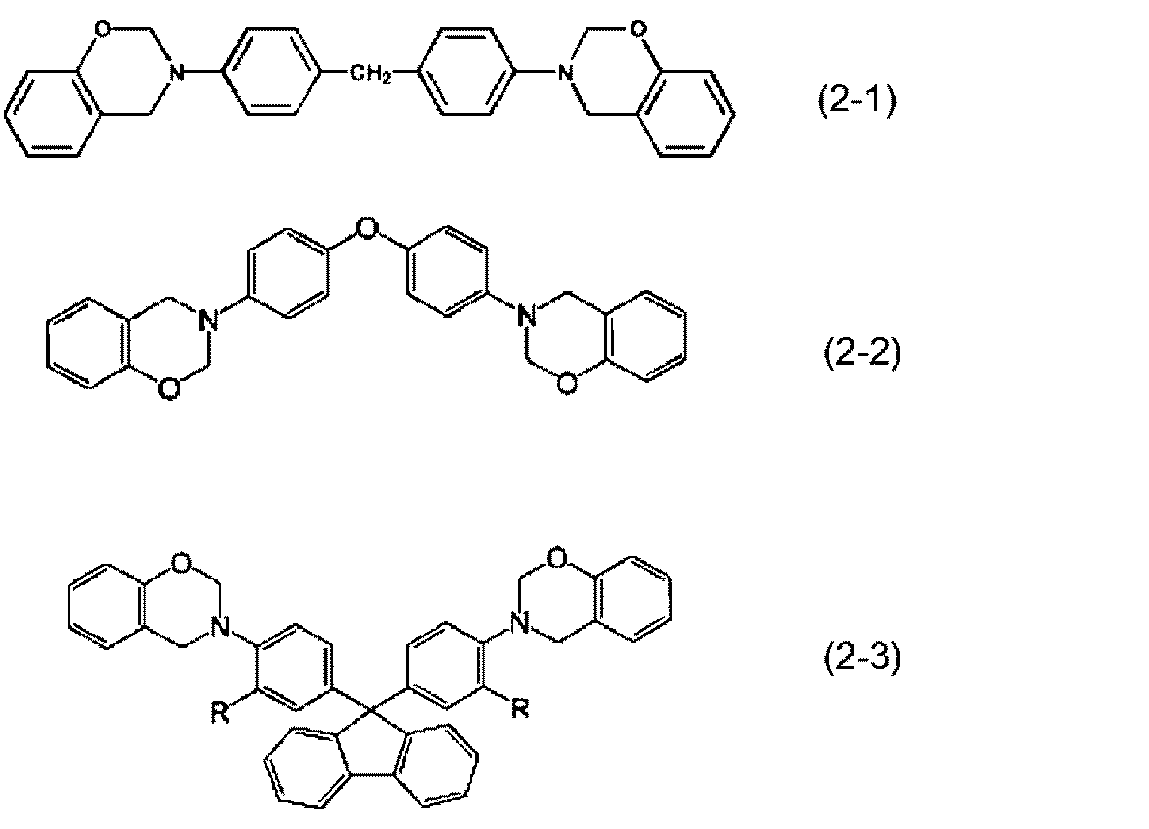


熱硬化性樹脂組成物中に含まれるベンゾオキサジン化合物の含有量は、特に限定されないが、熱硬化性樹脂組成物の全固形分(すなわち、溶媒を除く成分)を100重量%としたとき、1.0重量%以上25.0重量%以下が好ましく、3.0重量%以上20.0重量%以下がより好ましい。ベンゾオキサジン化合物の含有量が上記範囲内であると、得られる絶縁層の低熱収縮性および耐薬品性をより一層向上させることができる。
The content of the benzoxazine compound contained in the thermosetting resin composition is not particularly limited, but is 1 when the total solid content of the thermosetting resin composition (that is, the component excluding the solvent) is 100% by weight. 0.0 wt% or more and 25.0 wt% or less is preferable, and 3.0 wt% or more and 20.0 wt% or less is more preferable. When the content of the benzoxazine compound is within the above range, the low heat shrinkage and chemical resistance of the resulting insulating layer can be further improved.
(無機充填材)
本実施形態の熱硬化性樹脂組成物は、無機充填材を含むことができる。
無機充填材としては、例えば、タルク、焼成クレー、未焼成クレー、マイカ、ガラス等のケイ酸塩;酸化チタン、アルミナ、ベーマイト、シリカ、溶融シリカ等の酸化物;炭酸カルシウム、炭酸マグネシウム、ハイドロタルサイト等の炭酸塩;水酸化アルミニウム、水酸化マグネシウム、水酸化カルシウム等の水酸化物;硫酸バリウム、硫酸カルシウム、亜硫酸カルシウム等の硫酸塩または亜硫酸塩;ホウ酸亜鉛、メタホウ酸バリウム、ホウ酸アルミニウム、ホウ酸カルシウム、ホウ酸ナトリウム等のホウ酸塩;窒化アルミニウム、窒化ホウ素、窒化ケイ素、窒化炭素等の窒化物;チタン酸ストロンチウム、チタン酸バリウム等のチタン酸塩等を挙げることができる。
これらの中でも、タルク、アルミナ、ガラス、シリカ、マイカ、水酸化アルミニウム、水酸化マグネシウムが好ましく、シリカが特に好ましい。無機充填材としては、これらの中の1種類を単独で用いてもよく、2種類以上を併用してもよい。 (Inorganic filler)
The thermosetting resin composition of this embodiment can contain an inorganic filler.
Examples of inorganic fillers include silicates such as talc, calcined clay, unfired clay, mica, and glass; oxides such as titanium oxide, alumina, boehmite, silica, and fused silica; calcium carbonate, magnesium carbonate, and hydrotal Carbonates such as sites; hydroxides such as aluminum hydroxide, magnesium hydroxide, calcium hydroxide; sulfates or sulfites such as barium sulfate, calcium sulfate, calcium sulfite; zinc borate, barium metaborate, aluminum borate And borate salts such as calcium borate and sodium borate; nitrides such as aluminum nitride, boron nitride, silicon nitride and carbon nitride; titanates such as strontium titanate and barium titanate.
Among these, talc, alumina, glass, silica, mica, aluminum hydroxide, and magnesium hydroxide are preferable, and silica is particularly preferable. As the inorganic filler, one of these may be used alone, or two or more may be used in combination.
上記無機充填材の平均粒子径の下限値は、特に限定されないが、例えば、0.01μm以上が好ましく、0.05μm以上がより好ましく、0.5μm以上がさらに好ましい。これにより、上記熱硬化性樹脂のワニスの粘度が高くなるのを抑制でき、絶縁層作製時の作業性を向上させることができる。また、無機充填材の平均粒子径の上限値は、特に限定されないが、例えば、5.0μm以下が好ましく、2.0μm以下がより好ましく、1.0μm以下がさらに好ましい。これにより、上記熱硬化性樹脂のワニス中における無機充填材の沈降等の現象を抑制でき、より均一な樹脂膜を得ることができる。また、プリント配線基板の回路寸法L/Sが20μm/20μmを下回る際には、配線間の絶縁性に影響を与えるのを抑制することができる。
本実施形態において、無機充填材の平均粒子径は、例えば、レーザー回折式粒度分布測定装置(HORIBA社製、LA-500)により、粒子の粒度分布を体積基準で測定し、そのメディアン径(D50)を平均粒子径とすることができる。 Although the lower limit of the average particle diameter of the inorganic filler is not particularly limited, for example, 0.01 μm or more is preferable, 0.05 μm or more is more preferable, and 0.5 μm or more is more preferable. Thereby, it can suppress that the viscosity of the varnish of the said thermosetting resin becomes high, and can improve the workability | operativity at the time of insulation layer preparation. Moreover, the upper limit of the average particle diameter of the inorganic filler is not particularly limited, but is preferably 5.0 μm or less, more preferably 2.0 μm or less, and further preferably 1.0 μm or less. Thereby, phenomena, such as sedimentation of the inorganic filler in the varnish of the said thermosetting resin, can be suppressed, and a more uniform resin film can be obtained. Moreover, when the circuit dimension L / S of the printed wiring board is less than 20 μm / 20 μm, it is possible to suppress the influence on the insulation between the wirings.
In the present embodiment, the average particle size of the inorganic filler is determined by measuring the particle size distribution of the particles on a volume basis using, for example, a laser diffraction particle size distribution measuring apparatus (LA-500, manufactured by HORIBA), and the median diameter (D50 ) May be the average particle size.
また、本実施形態において、無機充填材の含有量が65重量%以上である場合には、当該無機充填材の平均粒子径の下限値は、例えば、0.5μm以上が好ましく、0.6μm以上がより好ましく、0.8μm以上がさらに好ましい。一方、当該無機充填材の平均粒子径の下限値は、たとえば、2μm以下が好ましく、1.9μm以下がより好ましく、1.8μm以下がさらに好ましい。無機充填材の含有量を上記範囲内とすることにより、樹脂膜の硬化物の反りを低減しつつ強度を一層高めることができる。
In the present embodiment, when the content of the inorganic filler is 65% by weight or more, the lower limit value of the average particle diameter of the inorganic filler is, for example, preferably 0.5 μm or more, and 0.6 μm or more. Is more preferable, and 0.8 μm or more is more preferable. On the other hand, the lower limit of the average particle diameter of the inorganic filler is, for example, preferably 2 μm or less, more preferably 1.9 μm or less, and even more preferably 1.8 μm or less. By setting the content of the inorganic filler within the above range, the strength can be further increased while reducing the warpage of the cured product of the resin film.
また、無機充填材は、特に限定されないが、平均粒子径が単分散の無機充填材を用いてもよいし、平均粒子径が多分散の無機充填材を用いてもよい。さらに平均粒子径が単分散および/または多分散の無機充填材を1種類または2種類以上で併用してもよい。
Further, the inorganic filler is not particularly limited, but an inorganic filler having a monodispersed average particle diameter may be used, or an inorganic filler having a polydispersed average particle diameter may be used. Furthermore, one type or two or more types of inorganic fillers having an average particle size of monodispersed and / or polydispersed may be used in combination.
上記無機充填材はシリカ粒子を含むことが好ましい。上記シリカ粒子の平均粒子径は、特に限定されないが、例えば、5.0μm以下が好ましく、0.1μm以上4.0μm以下がより好ましく、0.2μm以上2.0μm以下がさらに好ましい。使用するシリカ粒子の平均粒子径が上記範囲内であれば、無機充填材の樹脂膜への充填性をさらに向上させることができる。
The inorganic filler preferably contains silica particles. The average particle diameter of the silica particles is not particularly limited, but is preferably 5.0 μm or less, more preferably 0.1 μm or more and 4.0 μm or less, and further preferably 0.2 μm or more and 2.0 μm or less. When the average particle diameter of the silica particles used is within the above range, the filling property of the inorganic filler into the resin film can be further improved.
無機充填材の含有量の下限値は、熱硬化性樹脂組成物の全固形分100重量%に対して、特に限定されないが、例えば、65重量%以上が好ましく、70重量%以上がより好ましく、75重量%以上がさらに好ましい。これにより、樹脂膜の硬化物熱膨張率を特に低くすることができるとともに、その吸水率を特に低くすることができる。これにより、半導体パッケージの反りを抑制することができる。また、本実施形態の樹脂膜の硬化物は、高い伸び率を維持したまま、無機充填材の含有量を高めることができるので、応力緩和性を向上させることができる。一方で、無機充填材の含有量の上限値は、熱硬化性樹脂組成物の全固形分100重量%に対して、特に限定されないが、例えば、98重量%以下であることが好ましく、95重量%以下であることがより好ましく、90重量%以下であることがさらに好ましい。無機充填剤の含有量が上記範囲内であることにより、樹脂膜の硬化物の加工性を向上させることができる。
The lower limit of the content of the inorganic filler is not particularly limited with respect to 100% by weight of the total solid content of the thermosetting resin composition, for example, preferably 65% by weight or more, more preferably 70% by weight or more, More preferably 75% by weight or more. Thereby, while being able to make especially low the thermal expansion coefficient of the hardened | cured material of a resin film, the water absorption rate can be made especially low. Thereby, the curvature of a semiconductor package can be suppressed. Moreover, since the cured product of the resin film of the present embodiment can increase the content of the inorganic filler while maintaining a high elongation rate, the stress relaxation property can be improved. On the other hand, the upper limit of the content of the inorganic filler is not particularly limited with respect to 100% by weight of the total solid content of the thermosetting resin composition, but is preferably 98% by weight or less, for example, 95% by weight. % Or less, more preferably 90% by weight or less. When the content of the inorganic filler is within the above range, the workability of the cured product of the resin film can be improved.
(硬化剤)
本実施形態の熱硬化性樹脂組成物は、硬化剤を含むことができる。
上記硬化剤としては、特に限定されないが、例えば、ベンジルジメチルアミン(BDMA)、2,4,6-トリスジメチルアミノメチルフェノール(DMP-30)などの3級アミン化合物;2-メチルイミダゾール、2-エチル-4-メチルイミダゾール(EMI24)、2-フェニル-4-メチルイミダゾール(2P4MZ)、2-フェニルイミダゾール(2PZ)、2-フェニル-4-メチル-5-ヒドロキシイミダゾール(2P4MHZ)、1-ベンジル-2-フェニルイミダゾール(1B2PZ)などのイミダゾール化合物;BF3錯体などのルイス酸などの触媒型の硬化剤が挙げられる。
また、例えば、ジエチレントリアミン(DETA)、トリエチレンテトラミン(TETA)、メタキシレリレンジアミン(MXDA)などの脂肪族ポリアミン、m-フェニレンジアミン、p-フェニレンジアミン、o-キシレンジアミン、4,4'-ジアミノジフェニルメタン、4,4'-ジアミノジフェニルプロパン、4,4'-ジアミノジフェニルエーテル、4,4'-ジアミノジフェニルスルホン、3,3'-ジアミノジフェニルスルホン、1,5-ジアミノナフタレン、4,4'-(p-フェニレンジイソプロピリデン)ジアニリン、2,2-[4-(4-アミノフェノキシ)フェニル]プロパン、4,4'-ジアミノ-3,3'-ジメチルジフェニルメタン、4,4'-ジアミノ-3,3'-ジエチル-5,5'-ジメチルジフェニルメタン、3,3'-ジエチル-4,4'-ジアミノジフェニルメタンなどの芳香族ポリアミンのほか、ジシアンジアミド(DICY)、有機酸ジヒドララジドなどを含むポリアミン化合物;ヘキサヒドロ無水フタル酸(HHPA)、メチルテトラヒドロ無水フタル酸(MTHPA)などの脂環族酸無水物、無水トリメリット酸(TMA)、無水ピロメリット酸(PMDA)、ベンゾフェノンテトラカルボン酸(BTDA)などの芳香族酸無水物などを含む酸無水物;ポリサルファイド、チオエステル、チオエーテルなどのポリメルカプタン化合物;イソシアネートプレポリマー、ブロック化イソシアネートなどのイソシアネート化合物;カルボン酸含有ポリエステル樹脂などの有機酸類などの重付加型の硬化剤;2,2'-メチレンビス(4-エチル-6-tert-ブチルフェノール)、2,2'-メチレンビス(4-メチル-6-tert-ブチルフェノール)、4,4'-ブチリデンビス(3-メチル-6-tert-ブチルフェノール)、4,4'-チオビス(3-メチル-6-tert-ブチルフェノール)、2,6-ジ-tert-ブチル-4-メチルフェノール、2,5-ジ-tert-ブチルハイドロキノン、1,3,5-トリス(3,5-ジ-tert-ブチル-4-ヒドロキシベンジル)-1,3,5-トリアジン-2,4,6(1H,3H,5H)トリオンなどのフェノール系化合物も用いることができる。
さらに、第2硬化剤としては、例えば、ノボラック型フェノール樹脂、レゾール型フェノール樹脂などのフェノール樹脂系硬化剤;メチロール基含有尿素樹脂のような尿素樹脂;メチロール基含有メラミン樹脂のようなメラミン樹脂などの縮合型の硬化剤も用いてもよい。これらを単独で用いても2種以上を組み合わせて用いてもよい。 (Curing agent)
The thermosetting resin composition of the present embodiment can contain a curing agent.
The curing agent is not particularly limited. For example, tertiary amine compounds such as benzyldimethylamine (BDMA) and 2,4,6-trisdimethylaminomethylphenol (DMP-30); 2-methylimidazole, 2- Ethyl-4-methylimidazole (EMI24), 2-phenyl-4-methylimidazole (2P4MZ), 2-phenylimidazole (2PZ), 2-phenyl-4-methyl-5-hydroxyimidazole (2P4MHZ), 1-benzyl- imidazole compounds such as 2-phenylimidazole (1B2PZ); catalyst type curing agents include Lewis acids such as BF 3 complex.
Also, for example, aliphatic polyamines such as diethylenetriamine (DETA), triethylenetetramine (TETA), and metaxylylenediamine (MXDA), m-phenylenediamine, p-phenylenediamine, o-xylenediamine, 4,4′- Diaminodiphenylmethane, 4,4'-diaminodiphenylpropane, 4,4'-diaminodiphenyl ether, 4,4'-diaminodiphenylsulfone, 3,3'-diaminodiphenylsulfone, 1,5-diaminonaphthalene, 4,4'- (P-phenylenediisopropylidene) dianiline, 2,2- [4- (4-aminophenoxy) phenyl] propane, 4,4′-diamino-3,3′-dimethyldiphenylmethane, 4,4′-diamino-3 , 3'-diethyl-5,5'-dimethyldiphenylmethane, 3 In addition to aromatic polyamines such as 3'-diethyl-4,4'-diaminodiphenylmethane, polyamine compounds including dicyandiamide (DICY), organic acid dihydrazide, etc .; hexahydrophthalic anhydride (HHPA), methyltetrahydrophthalic anhydride (MTHPA) Acid anhydrides including aromatic acid anhydrides such as alicyclic acid anhydrides such as, trimellitic anhydride (TMA), pyromellitic anhydride (PMDA), benzophenone tetracarboxylic acid (BTDA); polysulfide, thioester, Polymercaptan compounds such as thioethers; isocyanate compounds such as isocyanate prepolymers and blocked isocyanates; polyaddition type curing agents such as organic acids such as carboxylic acid-containing polyester resins; 2,2′-methylenebis (4-ethyl-6- t ert-butylphenol), 2,2′-methylenebis (4-methyl-6-tert-butylphenol), 4,4′-butylidenebis (3-methyl-6-tert-butylphenol), 4,4′-thiobis (3- Methyl-6-tert-butylphenol), 2,6-di-tert-butyl-4-methylphenol, 2,5-di-tert-butylhydroquinone, 1,3,5-tris (3,5-di-tert) Phenolic compounds such as -butyl-4-hydroxybenzyl) -1,3,5-triazine-2,4,6 (1H, 3H, 5H) trione can also be used.
Furthermore, as the second curing agent, for example, a phenol resin-based curing agent such as a novolak type phenol resin or a resol type phenol resin; a urea resin such as a methylol group-containing urea resin; a melamine resin such as a methylol group-containing melamine resin; A condensation type curing agent may also be used. These may be used alone or in combination of two or more.
上記フェノール樹脂系硬化剤は、一分子内にフェノール性水酸基を2個以上有するモノマー、オリゴマー、ポリマー全般であり、その分子量、分子構造は特に限定されないが、例えば、フェノールノボラック樹脂、クレゾールノボラック樹脂、ナフトールノボラック樹脂などのノボラック型フェノール樹脂;トリフェノールメタン型フェノール樹脂などの多官能型フェノール樹脂;テルペン変性フェノール樹脂、ジシクロペンタジエン変性フェノール樹脂などの変性フェノール樹脂;フェニレン骨格および/またはビフェニレン骨格を有するフェノールアラルキル樹脂、フェニレンおよび/またはビフェニレン骨格を有するナフトールアラルキル樹脂などのアラルキル型樹脂;ビスフェノールA、ビスフェノールFなどのビスフェノール化合物等が挙げられる。これらは1種類を単独で用いても2種類以上を併用してもよい。これらのうち、硬化性の点から水酸基当量は90g/eq以上、250g/eq以下のフェノール樹脂系硬化剤を使用してもよい。
フェノール樹脂の重量平均分子量は、特に限定されないが、重量平均分子量4×10²以上1.8×10³以下が好ましく、5×10²以上1.5×10³以下がより好ましい。重量平均分子量を上記下限値以上とすることでプリプレグにタック性が生じるなどの問題がおこりにくくなり、上記上限値以下とすることで、プリプレグ作製時、繊維基材への含浸性が向上し、より均一な製品を得ることができる。 The phenol resin-based curing agent is a monomer, oligomer, or polymer in general having two or more phenolic hydroxyl groups in one molecule, and the molecular weight and molecular structure are not particularly limited. For example, phenol novolak resin, cresol novolak resin, Novolak type phenolic resin such as naphthol novolak resin; polyfunctional phenolic resin such as triphenolmethane type phenolic resin; modified phenolic resin such as terpene modified phenolic resin and dicyclopentadiene modified phenolic resin; phenylene skeleton and / or biphenylene skeleton Aralkyl resins such as phenol aralkyl resins, naphthol aralkyl resins having a phenylene and / or biphenylene skeleton; bisphenol compounds such as bisphenol A and bisphenol F Etc. The. These may be used alone or in combination of two or more. Among these, from the viewpoint of curability, a phenol resin-based curing agent having a hydroxyl group equivalent of 90 g / eq or more and 250 g / eq or less may be used.
The weight average molecular weight of the phenol resin is not particularly limited, but the weight average molecular weight is preferably 4 × 10 2 or more and 1.8 × 10 3 or less, more preferably 5 × 10 2 or more and 1.5 × 10 3 or less. By making the weight average molecular weight equal to or higher than the above lower limit value, problems such as tackiness occur in the prepreg, and by making the above upper limit value or less, the impregnation property to the fiber base material is improved at the time of prepreg production, A more uniform product can be obtained.
硬化剤の含有量の下限値は、熱硬化性樹脂組成物の全固形分100重量%に対して、特に限定されないが、例えば、0.01重量%以上が好ましく、0.05重量%以上がより好ましく、0.2重量%以上がさらに好ましい。硬化剤の含有量を上記下限値以上とすることにより、硬化を促進する効果を十分に発揮することができる。一方、硬化剤の含有量の上限値は、熱硬化性樹脂組成物の全固形分100重量%に対して、特に限定されないが、例えば、15重量%以下が好ましく、10重量%以下がより好ましく、8重量%以下がさらに好ましい。硬化剤の含有量が上記上限値以下であるとプリプレグの保存性をより向上させることができる。
The lower limit of the content of the curing agent is not particularly limited with respect to 100% by weight of the total solid content of the thermosetting resin composition, but is preferably 0.01% by weight or more, for example, 0.05% by weight or more. More preferred is 0.2% by weight or more. By setting the content of the curing agent to the above lower limit value or more, the effect of promoting curing can be sufficiently exhibited. On the other hand, the upper limit of the content of the curing agent is not particularly limited with respect to 100% by weight of the total solid content of the thermosetting resin composition, but is preferably 15% by weight or less, and more preferably 10% by weight or less. 8% by weight or less is more preferable. The preservability of a prepreg can be improved more as content of a hardening | curing agent is below the said upper limit.
(シアネート樹脂)
本実施形態の熱硬化性樹脂組成物は、シアネート樹脂をさらに含むことができる。
シアネート樹脂は、分子内にシアネート基(-O-CN)を有する樹脂であり、シアネート基を分子内に2個以上を有する樹脂を用いることができる。このようなシアネート樹脂としては、特に限定されないが、例えば、ハロゲン化シアン化合物とフェノール類やナフトール類とを反応させ、必要に応じて加熱等の方法でプレポリマー化することにより得ることができる。また、このようにして調製された市販品を用いることもできる。
シアネート樹脂を用いることにより、樹脂膜の硬化物の線膨張係数を小さくすることができる。さらに、樹脂膜の硬化物の電気特性(低誘電率、低誘電正接)、機械強度等を高めることができる。 (Cyanate resin)
The thermosetting resin composition of the present embodiment can further contain a cyanate resin.
The cyanate resin is a resin having a cyanate group (—O—CN) in the molecule, and a resin having two or more cyanate groups in the molecule can be used. Such a cyanate resin is not particularly limited. For example, it can be obtained by reacting a halogenated cyanide compound with phenols or naphthols, and prepolymerizing by a method such as heating as necessary. Moreover, the commercial item prepared in this way can also be used.
By using cyanate resin, the linear expansion coefficient of the cured resin film can be reduced. Furthermore, the electrical properties (low dielectric constant, low dielectric loss tangent), mechanical strength, etc. of the cured resin film can be enhanced.
シアネート樹脂は、例えば、ノボラック型シアネート樹脂;ビスフェノールA型シアネート樹脂、ビスフェノールE型シアネート樹脂、テトラメチルビスフェノールF型シアネート樹脂等のビスフェノール型シアネート樹脂;ナフトールアラルキル型フェノール樹脂と、ハロゲン化シアンとの反応で得られるナフトールアラルキル型シアネート樹脂;ジシクロペンタジエン型シアネート樹脂;ビフェニルアルキル型シアネート樹脂等を挙げることができる。これらの中でもノボラック型シアネート樹脂、ナフトールアラルキル型シアネート樹脂が好ましく、ノボラック型シアネート樹脂がより好ましい。ノボラック型シアネート樹脂を用いることにより、樹脂膜の硬化物の架橋密度が増加し、耐熱性が向上する。
Examples of the cyanate resin include novolak type cyanate resin; bisphenol type cyanate resin, bisphenol E type cyanate resin, bisphenol type cyanate resin such as tetramethylbisphenol F type cyanate resin; reaction of naphthol aralkyl type phenol resin and cyanogen halide. Naphthol aralkyl type cyanate resin obtained by the following: dicyclopentadiene type cyanate resin; biphenylalkyl type cyanate resin. Among these, novolak type cyanate resins and naphthol aralkyl type cyanate resins are preferable, and novolak type cyanate resins are more preferable. By using the novolac-type cyanate resin, the crosslink density of the cured product of the resin film is increased, and the heat resistance is improved.
この理由としては、ノボラック型シアネート樹脂は、硬化反応後にトリアジン環を形成することが挙げられる。さらに、ノボラック型シアネート樹脂は、その構造上ベンゼン環の割合が高く、炭化しやすいためと考えられる。また、ノボラック型シアネート樹脂を含む樹脂膜の硬化物は優れた剛性を有する。よって、樹脂膜の硬化物の耐熱性をより一層向上できる。
The reason for this is that the novolac-type cyanate resin forms a triazine ring after the curing reaction. Furthermore, it is considered that novolak-type cyanate resin has a high benzene ring ratio due to its structure and is easily carbonized. Moreover, the cured product of the resin film containing the novolak type cyanate resin has excellent rigidity. Therefore, the heat resistance of the cured resin film can be further improved.
ノボラック型シアネート樹脂としては、例えば、下記一般式(I)で示される樹脂を使用することができる。
As the novolac-type cyanate resin, for example, a resin represented by the following general formula (I) can be used.

一般式(I)で示されるノボラック型シアネート樹脂の平均繰り返し単位nは任意の整数である。平均繰り返し単位nは、特に限定されないが、1以上が好ましく、2以上がより好ましい。平均繰り返し単位nが上記下限値以上であると、ノボラック型シアネート樹脂の耐熱性が向上し、加熱時に低量体が脱離、揮発することを抑制できる。また、平均繰り返し単位nは、特に限定されないが、10以下が好ましく、7以下がより好ましい。nが上記上限値以下であると、溶融粘度が高くなるのを抑制でき、樹脂膜の成形性を向上させることができる。
The average repeating unit n of the novolak cyanate resin represented by the general formula (I) is an arbitrary integer. The average repeating unit n is not particularly limited, but is preferably 1 or more, and more preferably 2 or more. When the average repeating unit n is not less than the above lower limit, the heat resistance of the novolak cyanate resin is improved, and it is possible to suppress the demerization and volatilization of the low mer during heating. The average repeating unit n is not particularly limited, but is preferably 10 or less, more preferably 7 or less. It can suppress that melt viscosity becomes it high that n is below the said upper limit, and can improve the moldability of a resin film.
また、シアネート樹脂としては、下記一般式(II)で表わされるナフトールアラルキル型シアネート樹脂も好適に用いられる。下記一般式(II)で表わされるナフトールアラルキル型シアネート樹脂は、例えば、α-ナフトールあるいはβ-ナフトール等のナフトール類とp-キシリレングリコール、α,α'-ジメトキシ-p-キシレン、1,4-ジ(2-ヒドロキシ-2-プロピル)ベンゼン等との反応により得られるナフトールアラルキル型フェノール樹脂とハロゲン化シアンとを縮合させて得られる樹脂である。一般式(II)の繰り返し単位nは10以下の整数であることが好ましい。繰り返し単位nが10以下であると、より均一な樹脂膜を得ることができる。また、合成時に分子内重合が起こりにくく、水洗時の分液性が向上し、収量の低下を防止できる傾向がある。
As the cyanate resin, a naphthol aralkyl type cyanate resin represented by the following general formula (II) is also preferably used. The naphthol aralkyl type cyanate resin represented by the following general formula (II) includes, for example, naphthols such as α-naphthol or β-naphthol, p-xylylene glycol, α, α'-dimethoxy-p-xylene, 1,4 A resin obtained by condensing a naphthol aralkyl type phenol resin obtained by reaction with di (2-hydroxy-2-propyl) benzene or the like and cyanogen halide. The repeating unit n in the general formula (II) is preferably an integer of 10 or less. When the repeating unit n is 10 or less, a more uniform resin film can be obtained. In addition, intramolecular polymerization hardly occurs at the time of synthesis, the liquid separation property at the time of washing with water tends to be improved, and the decrease in yield tends to be prevented.

また、シアネート樹脂は1種類を単独で用いてもよいし、2種類以上を併用してもよく、1種類または2種類以上と、それらのプレポリマーとを併用してもよい。
In addition, one kind of cyanate resin may be used alone, two or more kinds may be used in combination, and one kind or two or more kinds and a prepolymer thereof may be used in combination.
シアネート樹脂の含有量の下限値は、熱硬化性樹脂組成物の全固形分100重量%に対して、たとえば、1重量%以上が好ましく、2重量%以上がより好ましく、3重量%以上がさらに好ましい。樹脂膜の硬化物の低線膨張化、高弾性率化を図ることができる。一方、シアネート樹脂の含有量の上限値は、熱硬化性樹脂組成物の全固形分100重量%に対して、特に限定されないが、例えば、30重量%以下が好ましく、25重量%以下がより好ましく、20重量%以下がさらに好ましい。耐熱性や耐湿性を向上させることができる。また、シアネート樹脂の含有量が上記範囲内であると、樹脂膜の硬化物の貯蔵弾性率E'をより一層向上させることができる。
The lower limit of the content of the cyanate resin is, for example, preferably 1% by weight or more, more preferably 2% by weight or more, and further more preferably 3% by weight or more with respect to 100% by weight of the total solid content of the thermosetting resin composition. preferable. It is possible to achieve low linear expansion and high elastic modulus of the cured resin film. On the other hand, the upper limit of the content of the cyanate resin is not particularly limited with respect to 100% by weight of the total solid content of the thermosetting resin composition, but is preferably 30% by weight or less, and more preferably 25% by weight or less. 20% by weight or less is more preferable. Heat resistance and moisture resistance can be improved. Further, when the content of the cyanate resin is within the above range, the storage elastic modulus E ′ of the cured product of the resin film can be further improved.
(フェノキシ樹脂)
本実施形態の熱硬化性樹脂組成物は、例えば、フェノキシ樹脂を含有してもよい。 (Phenoxy resin)
The thermosetting resin composition of this embodiment may contain a phenoxy resin, for example.
本実施形態の熱硬化性樹脂組成物は、例えば、フェノキシ樹脂を含有してもよい。 (Phenoxy resin)
The thermosetting resin composition of this embodiment may contain a phenoxy resin, for example.
上記フェノキシ樹脂としては、例えば、ビスフェノール骨格を有するフェノキシ樹脂、ナフタレン骨格を有するフェノキシ樹脂、アントラセン骨格を有するフェノキシ樹脂、ビフェニル骨格を有するフェノキシ樹脂などが挙げられる。また、これらの骨格を複数種有した構造のフェノキシ樹脂を用いることもできる。
Examples of the phenoxy resin include a phenoxy resin having a bisphenol skeleton, a phenoxy resin having a naphthalene skeleton, a phenoxy resin having an anthracene skeleton, and a phenoxy resin having a biphenyl skeleton. A phenoxy resin having a structure having a plurality of these skeletons can also be used.
これらの中でも、フェノキシ樹脂には、ビフェニル骨格およびビスフェノールS骨格を有するフェノキシ樹脂を用いるのが好ましい。ビフェニル骨格が有する剛直性により、フェノキシ樹脂のガラス転移温度を高くすることができるとともに、ビスフェノールS骨格の存在により、フェノキシ樹脂と金属との密着性を向上させることができる。その結果、絶縁層の耐熱性の向上を図ることができるとともに、絶縁層に対する配線層の密着性を向上させることができる。また、フェノキシ樹脂には、ビスフェノールA骨格およびビスフェノールF骨格を有するフェノキシ樹脂を用いるのも好ましい。これにより、配線層と絶縁層の密着性をさらに向上させることができる。
また、下記一般式(X)で表されるビスフェノールアセトフェノン構造を有するフェノキシ樹脂を用いるのも好ましい。 Among these, it is preferable to use a phenoxy resin having a biphenyl skeleton and a bisphenol S skeleton as the phenoxy resin. The rigidity of the biphenyl skeleton can increase the glass transition temperature of the phenoxy resin, and the presence of the bisphenol S skeleton can improve the adhesion between the phenoxy resin and the metal. As a result, the heat resistance of the insulating layer can be improved, and the adhesion of the wiring layer to the insulating layer can be improved. It is also preferable to use a phenoxy resin having a bisphenol A skeleton and a bisphenol F skeleton as the phenoxy resin. Thereby, the adhesiveness of a wiring layer and an insulating layer can further be improved.
It is also preferable to use a phenoxy resin having a bisphenolacetophenone structure represented by the following general formula (X).

(上記式(X)中、R1は互いに同一であっても異なっていてもよく、水素原子、炭素数1以上10以下の炭化水素基またはハロゲン元素から選ばれる基であり、R2は、水素原子、炭素数1以上10以下の炭化水素基またはハロゲン元素から選ばれる基であり、R3は、水素原子または炭素数1以上10以下の炭化水素基であり、mは0以上5以下の整数である。)
(In the formula (X), R 1 may be the being the same or different, a hydrogen atom, a group selected from a hydrocarbon group or a halogen element 1 to 10 carbon atoms, R 2 is A group selected from a hydrogen atom, a hydrocarbon group having 1 to 10 carbon atoms, or a halogen element, R 3 is a hydrogen atom or a hydrocarbon group having 1 to 10 carbon atoms, and m is 0 to 5 (It is an integer.)
ビスフェノールアセトフェノン構造を含むフェノキシ樹脂は、嵩高い構造を持っているため、溶剤溶解性や、配合する熱硬化性樹脂成分との相溶性に優れる。また、低粗度で均一な粗面を形成することができるため、絶縁層のSAP特性を向上させることができる。
Since the phenoxy resin containing a bisphenol acetophenone structure has a bulky structure, it has excellent solvent solubility and compatibility with the thermosetting resin component to be blended. In addition, since a uniform rough surface can be formed with low roughness, the SAP characteristics of the insulating layer can be improved.
ビスフェノールアセトフェノン構造を有するフェノキシ樹脂は、エポキシ樹脂とフェノール樹脂とを触媒で高分子量化させる方法等の公知の方法で合成することができる。
The phenoxy resin having a bisphenolacetophenone structure can be synthesized by a known method such as a method of increasing the molecular weight of an epoxy resin and a phenol resin using a catalyst.
ビスフェノールアセトフェノン構造を有するフェノキシ樹脂は、一般式(X)のビスフェノールアセトフェノン構造以外の構造が含まれていても良く、その構造はとくに限定されないが、ビスフェノールA型、ビスフェノールF型、ビスフェノールS型、ビフェニル型、フェノールノボラック型、クレゾールノボラック型の構造等が挙げられる。中でも、ビスフェノールアセトフェノン構造以外の構造として、ビフェニル型の構造を含むフェノキシ樹脂が、ガラス転移温度が高く好ましい。
The phenoxy resin having a bisphenol acetophenone structure may contain a structure other than the bisphenol acetophenone structure of the general formula (X), and the structure is not particularly limited, but bisphenol A type, bisphenol F type, bisphenol S type, biphenyl Type, phenol novolac type, cresol novolac type structure and the like. Among them, a phenoxy resin containing a biphenyl type structure as a structure other than the bisphenol acetophenone structure is preferable because of its high glass transition temperature.
ビスフェノールアセトフェノン構造を含むフェノキシ樹脂中の一般式(X)のビスフェノールアセトフェノン構造の含有量はとくに限定されないが、5モル%以上95モル%以下であることが好ましく、10モル%以上85モル%以下であることがより好ましく、15モル%以上75モル%以下であることがさらに好ましい。含有量が上記下限値以上であると、耐熱性、耐湿信頼性を向上させる効果を十分に発揮させることができる。また、含有量が上記上限値以下であると、溶剤溶解性を向上させることができる。
The content of the bisphenolacetophenone structure of the general formula (X) in the phenoxy resin containing a bisphenolacetophenone structure is not particularly limited, but is preferably 5 mol% or more and 95 mol% or less, and preferably 10 mol% or more and 85 mol% or less. More preferably, it is 15 mol% or more and 75 mol% or less. The effect which improves heat resistance and moisture-proof reliability can fully be exhibited as content is more than the said lower limit. Moreover, solvent solubility can be improved as content is below the said upper limit.
フェノキシ樹脂の重量平均分子量(Mw)の下限値は、例えば、10,000以上であることが好ましく、15,000以上であることがより好ましく、20,000以上であることがさらに好ましい。これにより、他の樹脂との相溶性や溶剤への溶解性を向上させることができる。一方、フェノキシ樹脂の重量平均分子量(Mw)の上限値は、例えば、60,000以下であることが好ましく、55,000以下であることがより好ましく、50,000以下であることがさらに好ましい。これにより、絶縁層の成膜性が向上し、プリント配線基板の製造に用いる場合に不具合が発生するのを抑制することができる。
The lower limit of the weight average molecular weight (Mw) of the phenoxy resin is, for example, preferably 10,000 or more, more preferably 15,000 or more, and further preferably 20,000 or more. Thereby, the compatibility with other resin and the solubility to a solvent can be improved. On the other hand, the upper limit value of the weight average molecular weight (Mw) of the phenoxy resin is, for example, preferably 60,000 or less, more preferably 55,000 or less, and further preferably 50,000 or less. Thereby, the film formability of an insulating layer improves and it can suppress that a malfunction generate | occur | produces, when using it for manufacture of a printed wiring board.
フェノキシ樹脂の含有量は、とくに限定されないが、無機充填材を除く熱硬化性樹脂組成物全体に対して、0.5重量%以上40重量%以下であることが好ましく、1重量%以上20重量%以下であることがより好ましい。含有量が上記下限値以上であると、絶縁層の機械強度の低下や、絶縁層と導体回路とのメッキ密着性の低下を抑制することができる。上記上限値以下であると、絶縁層の熱膨張率の増加を抑制でき、耐熱性の低下を抑制することができる。
The content of the phenoxy resin is not particularly limited, but is preferably 0.5% by weight or more and 40% by weight or less, and preferably 1% by weight or more and 20% by weight or less with respect to the entire thermosetting resin composition excluding the inorganic filler. % Or less is more preferable. When the content is equal to or higher than the lower limit, it is possible to suppress a decrease in mechanical strength of the insulating layer and a decrease in plating adhesion between the insulating layer and the conductor circuit. When it is not more than the above upper limit, an increase in the coefficient of thermal expansion of the insulating layer can be suppressed, and a decrease in heat resistance can be suppressed.
(硬化促進剤)
本実施形態の熱硬化性樹脂組成物は、例えば、硬化促進剤を含んでもよい。これにより、熱硬化性樹脂組成物の硬化性を向上させることができる。硬化促進剤としては、熱硬化性樹脂の硬化反応を促進させる化合物を用いることができ、その種類は特に限定されない。本実施形態においては、硬化促進剤として、例えば、ナフテン酸亜鉛、ナフテン酸コバルト、オクチル酸スズ、オクチル酸コバルト、オクチル酸亜鉛、ビスアセチルアセトナートコバルト(II)、トリスアセチルアセトナートコバルト(III)等の有機金属塩、トリエチルアミン、トリブチルアミン、ジアザビシクロ[2,2,2]オクタン等の3級アミン類、2-フェニルイミダゾール、2-フェニル-4-メチルイミダゾール、2-エチル-4-エチルイミダゾール、2-フェニル-4-エチルイミダゾール、2-フェニル-4-メチル-5-ヒドロキシイミダゾール、2-フェニル-4-メチル-5-ヒドロキシメチルイミダゾール、2-フェニル-4,5-ジヒドロキシイミダゾール等のイミダゾール類、フェノール、ビスフェノールA、ノニルフェノール等のフェノール化合物、酢酸、安息香酸、サリチル酸、パラトルエンスルホン酸等の有機酸、およびオニウム塩化合物から選択される一種または二種以上を含むことができる。これらの中でも、硬化性をより効果的に向上させる観点からは、オニウム塩化合物を含むことがより好ましい。 (Curing accelerator)
The thermosetting resin composition of this embodiment may contain a hardening accelerator, for example. Thereby, the sclerosis | hardenability of a thermosetting resin composition can be improved. As a hardening accelerator, the compound which accelerates | stimulates hardening reaction of a thermosetting resin can be used, The kind is not specifically limited. In this embodiment, as a hardening accelerator, for example, zinc naphthenate, cobalt naphthenate, tin octylate, cobalt octylate, zinc octylate, bisacetylacetonate cobalt (II), trisacetylacetonate cobalt (III) Organic metal salts such as triethylamine, tributylamine, tertiary amines such as diazabicyclo [2,2,2] octane, 2-phenylimidazole, 2-phenyl-4-methylimidazole, 2-ethyl-4-ethylimidazole, Imidazoles such as 2-phenyl-4-ethylimidazole, 2-phenyl-4-methyl-5-hydroxyimidazole, 2-phenyl-4-methyl-5-hydroxymethylimidazole, 2-phenyl-4,5-dihydroxyimidazole , Phenol, bisphe Lumpur A, phenolic compounds nonylphenol, acetic, benzoic acid, salicylic, organic acids such as p-toluenesulfonic acid, and one or more selected from an onium salt compound. Among these, it is more preferable to include an onium salt compound from the viewpoint of more effectively improving curability.
硬化促進剤として用いられるオニウム塩化合物は、特に限定されないが、例えば、下記一般式(2)で表される化合物を用いることができる。
Although the onium salt compound used as a curing accelerator is not particularly limited, for example, a compound represented by the following general formula (2) can be used.

硬化促進剤の含有量の下限値は、例えば、熱硬化性樹脂組成物の全固形分100重量%に対して、たとえば、0.01重量%以上が好ましく、0.05重量%以上がより好ましい。硬化促進剤の含有量を上記下限値以上とすることにより、熱硬化性樹脂組成物の硬化性をより効果的に向上させることができる。一方、硬化促進剤の含有量の上限値は、例えば、熱硬化性樹脂組成物の全固形分100重量%に対して、2.5重量%以下が好ましく、1重量%以下がより好ましい。硬化促進剤の含有量を上記上限値以下とすることにより、熱硬化性樹脂組成物の保存性を向上させることができる。
The lower limit of the content of the curing accelerator is, for example, preferably 0.01% by weight or more and more preferably 0.05% by weight or more with respect to 100% by weight of the total solid content of the thermosetting resin composition. . By making content of a hardening accelerator more than the said lower limit, sclerosis | hardenability of a thermosetting resin composition can be improved more effectively. On the other hand, the upper limit value of the content of the curing accelerator is, for example, preferably 2.5% by weight or less and more preferably 1% by weight or less with respect to 100% by weight of the total solid content of the thermosetting resin composition. By making content of a hardening accelerator into the said upper limit or less, the preservability of a thermosetting resin composition can be improved.
(カップリング剤)
本実施形態の熱硬化性樹脂組成物は、カップリング剤を含んでもよい。カップリング剤は熱硬化性樹脂組成物の調製時に直接添加してもよいし、無機充填材にあらかじめ添加しておいてもよい。カップリング剤の使用により無機充填材と各樹脂との界面の濡れ性を向上させることができる。したがって、カップリング剤を使用することは好ましく、樹脂膜の硬化物の耐熱性を改良することができる。また、カップリング剤を用いることにより、銅箔との密着性を向上させることができる。さらに、吸湿耐性を向上できるので、湿度環境下後においても、銅箔との密着性を維持することができる。 (Coupling agent)
The thermosetting resin composition of this embodiment may contain a coupling agent. The coupling agent may be added directly when preparing the thermosetting resin composition, or may be added in advance to the inorganic filler. Use of a coupling agent can improve the wettability of the interface between the inorganic filler and each resin. Therefore, it is preferable to use a coupling agent, and the heat resistance of the cured resin film can be improved. Moreover, adhesiveness with copper foil can be improved by using a coupling agent. Furthermore, since the moisture absorption resistance can be improved, the adhesion with the copper foil can be maintained even after the humidity environment.
カップリング剤としては、例えば、エポキシシランカップリング剤、カチオニックシランカップリング剤、アミノシランカップリング剤等のシランカップリング剤、チタネート系カップリング剤およびシリコーンオイル型カップリング剤等が挙げられる。カップリング剤は一種類を単独で用いてもよいし、二種類以上を併用してもよい。本実施形態において、カップリング剤はシランカップリング剤を含有してもよい。
これにより、無機充填材と各樹脂との界面の濡れ性を高くすることができ、樹脂膜の硬化物の耐熱性をより向上させることができる。 Examples of the coupling agent include silane coupling agents such as epoxy silane coupling agents, cationic silane coupling agents, and amino silane coupling agents, titanate coupling agents, and silicone oil type coupling agents. A coupling agent may be used individually by 1 type, and may use 2 or more types together. In this embodiment, the coupling agent may contain a silane coupling agent.
Thereby, the wettability of the interface of an inorganic filler and each resin can be made high, and the heat resistance of the hardened | cured material of a resin film can be improved more.
シランカップリング剤としては、特に限定されないが、例えば、エポキシシラン、アミノシラン、アルキルシラン、ウレイドシラン、メルカプトシラン、ビニルシラン等が挙げられる。
The silane coupling agent is not particularly limited, and examples thereof include epoxy silane, amino silane, alkyl silane, ureido silane, mercapto silane, and vinyl silane.
具体的な化合物としては、例えば、γ-アミノプロピルトリエトキシシラン、γ-アミノプロピルトリメトキシシラン、N-β(アミノエチル)γ-アミノプロピルトリメトキシシラン、N-β(アミノエチル)γ-アミノプロピルメチルジメトキシシラン、N-フェニルγ-アミノプロピルトリエトキシシラン、N-フェニルγ-アミノプロピルトリメトキシシラン、N-β(アミノエチル)γ-アミノプロピルトリエトキシシラン、N-6-(アミノヘキシル)3-アミノプロピルトリメトキシシラン、N-(3-(トリメトキシシリルプロピル)-1,3-ベンゼンジメタナン、γ-グリシドキシプロピルトリエトキシシラン、γ-グリシドキシプロピルトリメトキシシラン、γ-グリシドキシプロピルメチルジメトキシシラン、β-(3,4-エポキシシクロヘキシル)エチルトリメトキシシラン、γ-メルカプトプロピルトリメトキシシラン、メチルトリメトキシシラン、γ-ウレイドプロピルトリエトキシシラン、ビニルトリエトキシシラン等が挙げられ、これらのうちの一種または二種以上を組み合せて用いることができる。これらのうちエポキシシラン、メルカプトシラン、アミノシランが好ましく、アミノシランとしては、1級アミノシラン又はアニリノシランがより好ましい。
Specific examples of the compound include γ-aminopropyltriethoxysilane, γ-aminopropyltrimethoxysilane, N-β (aminoethyl) γ-aminopropyltrimethoxysilane, and N-β (aminoethyl) γ-amino. Propylmethyldimethoxysilane, N-phenylγ-aminopropyltriethoxysilane, N-phenylγ-aminopropyltrimethoxysilane, N-β (aminoethyl) γ-aminopropyltriethoxysilane, N-6- (aminohexyl) 3-aminopropyltrimethoxysilane, N- (3- (trimethoxysilylpropyl) -1,3-benzenedimethanane, γ-glycidoxypropyltriethoxysilane, γ-glycidoxypropyltrimethoxysilane, γ -Glycidoxypropylmethyldimethoxysilane, β- (3,4 -Epoxycyclohexyl) ethyltrimethoxysilane, γ-mercaptopropyltrimethoxysilane, methyltrimethoxysilane, γ-ureidopropyltriethoxysilane, vinyltriethoxysilane, etc., one or a combination of two or more of these Of these, epoxy silane, mercapto silane, and amino silane are preferable, and the amino silane is more preferably primary amino silane or anilino silane.
カップリング剤の添加量は、無機充填材の比表面積に対して適切に調整することができる。このようなカップリング剤の添加量の下限値は、例えば、熱硬化性樹脂組成物の全固形分100重量%に対して、0.01重量%以上が好ましく、0.05重量%以上がより好ましい。カップリング剤の含有量が上記下限値以上であると、無機充填材を十分に被覆することができ、樹脂膜の硬化物の耐熱性を向上させることができる。一方、カップリング剤の添加量の上限値は、例えば、熱硬化性樹脂組成物の全固形分100重量%に対して、3重量%以下が好ましく、1.5重量%以下がより好ましい。カップリング剤の含有量が上記上限値以下であると、反応に影響を与えるのを抑制でき、樹脂膜の硬化物の曲げ強度等の低下を抑制することができる。
The addition amount of the coupling agent can be appropriately adjusted with respect to the specific surface area of the inorganic filler. The lower limit of the amount of coupling agent added is, for example, preferably 0.01% by weight or more, more preferably 0.05% by weight or more with respect to 100% by weight of the total solid content of the thermosetting resin composition. preferable. When the content of the coupling agent is not less than the above lower limit, the inorganic filler can be sufficiently covered, and the heat resistance of the cured product of the resin film can be improved. On the other hand, the upper limit of the addition amount of the coupling agent is preferably, for example, 3% by weight or less, more preferably 1.5% by weight or less, with respect to 100% by weight of the total solid content of the thermosetting resin composition. When the content of the coupling agent is not more than the above upper limit value, it is possible to suppress the influence on the reaction, and it is possible to suppress a decrease in the bending strength or the like of the cured product of the resin film.
(添加剤)
なお、本実施形態の熱硬化性樹脂組成物は、本発明の目的を損なわない範囲で、緑、赤、青、黄、および黒等の染料、黒色顔料な等の顔料、色素のうちの少なくとも一種以上を含む着色剤、低応力剤、消泡剤、レベリング剤、紫外線吸収剤、発泡剤、酸化防止剤、難燃剤、イオン捕捉剤等の上記成分(熱硬化性樹脂、硬化剤、無機充填材、硬化促進剤、カップリング剤)以外の添加剤を含んでもよい。これらを単独で用いても2種以上を組み合わせて用いてもよい。 (Additive)
The thermosetting resin composition of the present embodiment is a dye such as green, red, blue, yellow, and black, a pigment such as a black pigment, and a dye within a range that does not impair the object of the present invention. One or more colorants, low-stress agents, antifoaming agents, leveling agents, UV absorbers, foaming agents, antioxidants, flame retardants, ion scavengers, and other components (thermosetting resins, curing agents, inorganic fillers) Additives other than materials, curing accelerators, and coupling agents) may be included. These may be used alone or in combination of two or more.
本実施形態の熱硬化性樹脂組成物は、低応力剤やゴム成分を含有しなくてもよい。この場合でも、本実施形態の熱硬化性樹脂組成物の硬化物は、無機充填材の充填率を高めつつ、低弾性率とすることができるので、基板プロセス中における反りや搬送中の衝撃によるクラックを抑制することができる。
The thermosetting resin composition of the present embodiment may not contain a low stress agent or a rubber component. Even in this case, the cured product of the thermosetting resin composition of the present embodiment can be made to have a low elastic modulus while increasing the filling rate of the inorganic filler, so that it is caused by warpage during the substrate process or impact during transportation. Cracks can be suppressed.
顔料としては、カオリン、合成酸化鉄赤、カドミウム黄、ニッケルチタン黄、ストロンチウム黄、含水酸化クロム、酸化クロム、アルミ酸コバルト、合成ウルトラマリン青等の無機顔料、フタロシアニン等の多環顔料、アゾ顔料等が挙げられる。
Examples of pigments include kaolin, synthetic iron oxide red, cadmium yellow, nickel titanium yellow, strontium yellow, hydrous chromium oxide, chromium oxide, cobalt aluminate, synthetic ultramarine blue, etc., polycyclic pigments such as phthalocyanine, azo pigments Etc.
染料としては、イソインドリノン、イソインドリン、キノフタロン、キサンテン、ジケトピロロピロール、ペリレン、ペリノン、アントラキノン、インジゴイド、オキサジン、キナクリドン、ベンツイミダゾロン、ビオランスロン、フタロシアニン、アゾメチン等が挙げられる。
Examples of the dye include isoindolinone, isoindoline, quinophthalone, xanthene, diketopyrrolopyrrole, perylene, perinone, anthraquinone, indigoid, oxazine, quinacridone, benzimidazolone, violanthrone, phthalocyanine, azomethine and the like.
本実施形態において、ワニス状の熱硬化性樹脂組成物は、溶剤を含むことができる。
上記溶剤としては、たとえばアセトン、メチルエチルケトン、メチルイソブチルケトン、トルエン、酢酸エチル、ヘプタン、シクロヘキサン、シクロヘキサノン、テトラヒドロフラン、ジメチルホルムアミド、ジメチルアセトアミド、ジメチルスルホキシド、エチレングリコール、セルソルブ系、カルビトール系、アニソール、およびN-メチルピロリドン等の有機溶剤が挙げられる。これらを単独で用いても2種以上を組み合わせて用いてもよい。 In this embodiment, the varnish-like thermosetting resin composition can contain a solvent.
Examples of the solvent include acetone, methyl ethyl ketone, methyl isobutyl ketone, toluene, ethyl acetate, heptane, cyclohexane, cyclohexanone, tetrahydrofuran, dimethylformamide, dimethylacetamide, dimethyl sulfoxide, ethylene glycol, cellosolve, carbitol, anisole, and N -Organic solvents such as methylpyrrolidone. These may be used alone or in combination of two or more.
熱硬化性樹脂組成物がワニス状である場合において、熱硬化性樹脂組成物の固形分含有量は、たとえば30重量%以上80重量%以下が好ましく、40重量%以上70重量%以下がより好ましい。これにより、作業性や成膜性に非常に優れた熱硬化性樹脂組成物が得られる。
When the thermosetting resin composition is varnished, the solid content of the thermosetting resin composition is preferably, for example, 30% by weight to 80% by weight, and more preferably 40% by weight to 70% by weight. . Thereby, the thermosetting resin composition excellent in workability | operativity and film formability is obtained.
ワニス状の熱硬化性樹脂組成物は、上述の各成分を、たとえば、超音波分散方式、高圧衝突式分散方式、高速回転分散方式、ビーズミル方式、高速せん断分散方式、および自転公転式分散方式などの各種混合機を用いて溶剤中に溶解、混合、撹拌することにより調製することができる。
The varnish-like thermosetting resin composition comprises the above-described components, for example, an ultrasonic dispersion method, a high-pressure collision dispersion method, a high-speed rotation dispersion method, a bead mill method, a high-speed shear dispersion method, and a rotation and revolution dispersion method. It can prepare by melt | dissolving in a solvent, mixing, and stirring using various mixers of these.
次いで、本実施形態の樹脂膜について説明する。
Next, the resin film of this embodiment will be described.
本実施形態の樹脂膜は、ワニス状である上記熱硬化性樹脂組成物をフィルム化することにより得ることができる。例えば、本実施形態の樹脂膜は、ワニス状の熱硬化性樹脂組成物を塗布して得られた塗布膜に対して、溶剤を除去することにより得ることができる。このような樹脂膜においては、溶剤含有率が樹脂膜全体に対して5重量%以下とすることができる。本実施形態において、たとえば100℃~150℃、1分~5分の条件で溶剤を除去する工程を実施してもよい。これにより、熱硬化性樹脂を含む樹脂膜の硬化が進行することを抑制しつつ、十分に溶剤を除去することが可能となる。
The resin film of the present embodiment can be obtained by forming a film of the thermosetting resin composition having a varnish shape. For example, the resin film of this embodiment can be obtained by removing the solvent from the coating film obtained by coating a varnish-like thermosetting resin composition. In such a resin film, the solvent content can be 5% by weight or less based on the entire resin film. In the present embodiment, for example, a step of removing the solvent may be performed under conditions of 100 ° C. to 150 ° C. and 1 minute to 5 minutes. Thereby, it is possible to sufficiently remove the solvent while suppressing the curing of the resin film containing the thermosetting resin.
(キャリア付き樹脂膜)
次いで、本実施形態のキャリア付樹脂膜について説明する。
図1は、本実施形態におけるキャリア付樹脂膜100の構成の一例を示す断面図である。
本実施形態のキャリア付樹脂膜100は、図1に示すように、キャリア基材12と、キャリア基材12上に設けられた、上記熱硬化性樹脂組成物から形成される樹脂膜10と、を備えることができる。これにより、樹脂膜10のハンドリング性を向上させることができる。 (Resin film with carrier)
Next, the resin film with a carrier of this embodiment will be described.
FIG. 1 is a cross-sectional view showing an example of the configuration of the resin film withcarrier 100 in the present embodiment.
As shown in FIG. 1, the resin film with acarrier 100 of the present embodiment includes a carrier base material 12 and a resin film 10 formed on the carrier base material 12 and formed from the thermosetting resin composition. Can be provided. Thereby, the handleability of the resin film 10 can be improved.
次いで、本実施形態のキャリア付樹脂膜について説明する。
図1は、本実施形態におけるキャリア付樹脂膜100の構成の一例を示す断面図である。
本実施形態のキャリア付樹脂膜100は、図1に示すように、キャリア基材12と、キャリア基材12上に設けられた、上記熱硬化性樹脂組成物から形成される樹脂膜10と、を備えることができる。これにより、樹脂膜10のハンドリング性を向上させることができる。 (Resin film with carrier)
Next, the resin film with a carrier of this embodiment will be described.
FIG. 1 is a cross-sectional view showing an example of the configuration of the resin film with
As shown in FIG. 1, the resin film with a
キャリア付樹脂膜100は、巻き取り可能なロール形状でも、矩形形状などの枚葉形状であってもよい。
The resin film with carrier 100 may be a roll shape that can be wound or a single wafer shape such as a rectangular shape.
本実施形態において、キャリア基材12としては、例えば、高分子フィルムや金属箔などを用いることができる。当該高分子フィルムとしては、特に限定されないが、例えば、ポリエチレン、ポリプロピレン等のポリオレフィン、ポリエチレンテレフタレート、ポリブチレンテレフタレートなどのポリエステル、ポリカーボネート、シリコーンシート等の離型紙、フッ素系樹脂、ポリイミド樹脂などの耐熱性を有した熱可塑性樹脂シート等が挙げられる。当該金属箔としては、特に限定されないが、例えば、銅または銅系合金、アルミまたはアルミ系合金、鉄または鉄系合金、銀または銀系合金、金または金系合金、亜鉛または亜鉛系合金、ニッケルまたはニッケル系合金、錫または錫系合金等が挙げられる。これらの中でも、ポリエチレンテレフタレートで構成されるシートが安価および剥離強度の調節が簡便なため最も好ましい。かかる材料で構成されるシートをキャリア基材12として用いることにより、樹脂膜10をキャリア基材12から、適度な強度で剥離することが容易となる。
In the present embodiment, for example, a polymer film or a metal foil can be used as the carrier substrate 12. The polymer film is not particularly limited. For example, polyolefin such as polyethylene and polypropylene, polyester such as polyethylene terephthalate and polybutylene terephthalate, release paper such as polycarbonate and silicone sheet, heat resistance such as fluorine resin and polyimide resin. A thermoplastic resin sheet having The metal foil is not particularly limited. For example, copper or copper alloy, aluminum or aluminum alloy, iron or iron alloy, silver or silver alloy, gold or gold alloy, zinc or zinc alloy, nickel Alternatively, a nickel-based alloy, tin, a tin-based alloy, or the like can be given. Among these, a sheet made of polyethylene terephthalate is most preferable because it is inexpensive and easy to adjust the peel strength. By using a sheet made of such a material as the carrier substrate 12, it becomes easy to peel the resin film 10 from the carrier substrate 12 with an appropriate strength.
樹脂膜10の厚みの下限値は、特に限定されないが、例えば、1μm以上が好ましく、3μm以上がより好ましく、5μm以上がさらに好ましい。これにより、樹脂膜10の機械強度を高めることができる。一方、樹脂膜10の厚みの上限値は、特に限定されないが、例えば、500μm以下が好ましく、300μm以下がより好ましく、100μm以下がさらに好ましい。これにより、半導体装置の薄層化を図ることができる。
The lower limit of the thickness of the resin film 10 is not particularly limited, but is preferably 1 μm or more, more preferably 3 μm or more, and further preferably 5 μm or more. Thereby, the mechanical strength of the resin film 10 can be increased. On the other hand, the upper limit value of the thickness of the resin film 10 is not particularly limited, but is preferably 500 μm or less, more preferably 300 μm or less, and even more preferably 100 μm or less. Thereby, the semiconductor device can be thinned.
キャリア基材の厚みは、特に限定されないが、例えば、10~100μmが好ましく、10~70μmがより好ましい。これにより、キャリア付樹脂膜100を製造する際の取り扱い性がより良好となる。
The thickness of the carrier substrate is not particularly limited, but is preferably 10 to 100 μm, for example, and more preferably 10 to 70 μm. Thereby, the handleability at the time of manufacturing the resin film 100 with a carrier becomes more favorable.
本実施形態のキャリア付樹脂膜100は、単層でも多層でもよく、1種または2種以上の樹脂膜10を含むことができる。当該樹脂シートが多層の場合には、各樹脂シートが同種で構成されてもよく、異種で構成されてもよい。また、キャリア付樹脂膜100は、樹脂膜10上の最外層側に、保護膜を有していてもよい。
The resin film with carrier 100 of the present embodiment may be a single layer or a multilayer, and may include one or more types of resin films 10. When the resin sheet is multi-layered, the resin sheets may be composed of the same kind or different kinds. The resin film with carrier 100 may have a protective film on the outermost layer side on the resin film 10.
本実施形態において、キャリア付樹脂膜100を形成する方法としては、特に限定されない。かかる方法としては、例えば、ワニス状の熱硬化性樹脂組成物をキャリア基材12上に、各種コーター装置を用いて塗布することにより塗布膜を形成した後、当該塗布膜を適切に乾燥させることにより溶剤を除去する方法を用いることができる。
In the present embodiment, the method for forming the resin film with carrier 100 is not particularly limited. As such a method, for example, a coating film is formed by applying a varnish-like thermosetting resin composition on the carrier substrate 12 using various coater apparatuses, and then the coating film is appropriately dried. Can be used to remove the solvent.
本実施形態の樹脂膜の特性について説明する。
The characteristics of the resin film of this embodiment will be described.
本実施形態の樹脂膜は、前述の通り、上記熱硬化性樹脂組成物から形成される樹脂膜である。
本実施形態の上記樹脂膜の硬化物において、低弾性特性と高伸度特性を両立することができるので、優れた強靱性を実現することができる。 As described above, the resin film of the present embodiment is a resin film formed from the thermosetting resin composition.
Since the cured product of the resin film of the present embodiment can achieve both low elastic properties and high elongation properties, excellent toughness can be realized.
本実施形態における熱硬化性樹脂組成物の硬化物に対して動的粘弾性測定を行ったときに、かかる硬化物の30℃における貯蔵弾性率E'30の上限値は、10GPa以下であるが、9GPa以下であることが好ましく、8GPa以下であることがより好ましい。これにより、低弾性に優れた樹脂膜の硬化物を実現できる。一方、上記30℃における貯蔵弾性率E'30の下限値は、1GPa以上である。これにより、所定の弾性率が得られるため、強度に優れた樹脂膜の硬化物が得られる。
When dynamic viscoelasticity measurement is performed on the cured product of the thermosetting resin composition in the present embodiment, the upper limit value of the storage elastic modulus E ′ 30 at 30 ° C. of the cured product is 10 GPa or less. , 9 GPa or less is preferable, and 8 GPa or less is more preferable. Thereby, the hardened | cured material of the resin film excellent in low elasticity is realizable. On the other hand, the lower limit value of the storage elastic modulus E ′ 30 at 30 ° C. is 1 GPa or more. Thereby, since a predetermined elastic modulus is obtained, a cured product of the resin film having excellent strength can be obtained.
本実施形態における熱硬化性樹脂組成物の硬化物に対して引張り試験を行ったときに、硬化物の引張り伸び率の下限値は、2%以上であるが、3%以上であることが好ましく、4%以上であることがより好ましい。これにより、柔軟性や伸び性に優れた樹脂膜の硬化物が得られる。また、無機充填材を高充填しつつも高い伸び性を有する樹脂膜の硬化物が得られる。一方、上記引張り伸び率の上限値は、特に限定されないが、例えば、40%以下としてもよい。
本実施形態において、上記貯蔵弾性率を低減しつつ上記引張り伸び率を高められるため、強靱性に優れた樹脂膜の硬化物が得られる。 When a tensile test is performed on the cured product of the thermosetting resin composition in the present embodiment, the lower limit value of the tensile elongation rate of the cured product is 2% or more, preferably 3% or more. More preferably, it is 4% or more. Thereby, the cured | curing material of the resin film excellent in the softness | flexibility and extensibility is obtained. In addition, a cured product of a resin film having high elongation while being highly filled with an inorganic filler can be obtained. On the other hand, the upper limit value of the tensile elongation is not particularly limited, but may be 40% or less, for example.
In the present embodiment, since the tensile elongation can be increased while reducing the storage elastic modulus, a cured resin film having excellent toughness can be obtained.
本実施形態において、熱硬化性樹脂組成物の硬化物のガラス転移温度の下限値は、特に限定されないが、例えば、10℃以上が好ましく、15℃以上がより好ましく、20℃以上がさらに好ましい。硬化物のガラス転移温度を室温25℃±約10℃の範囲内とすることにより、実温における上記硬化物の弾性特性と伸び特性とがより優れる。これにより、搬送時における基板の反りやクラックを十分に抑制することができる。また、上記ガラス転移温度の上限値は、特に限定されないが、例えば、220℃以下としてもよく、110℃以下が好ましく、80℃以下がより好ましく、35℃以下がさらに好ましい。
In this embodiment, the lower limit of the glass transition temperature of the cured product of the thermosetting resin composition is not particularly limited, but is preferably 10 ° C. or higher, more preferably 15 ° C. or higher, and further preferably 20 ° C. or higher. By setting the glass transition temperature of the cured product within the range of room temperature 25 ° C. ± about 10 ° C., the elastic properties and elongation properties of the cured product at the actual temperature are more excellent. Thereby, the curvature and crack of a board | substrate at the time of conveyance can fully be suppressed. Moreover, although the upper limit of the said glass transition temperature is not specifically limited, For example, it is good also as 220 degrees C or less, 110 degrees C or less is more preferable, 80 degrees C or less is more preferable, and 35 degrees C or less is further more preferable.
本実施形態において、熱硬化性樹脂組成物の硬化物の損失正接tanδのピーク値の下限値は、例えば、0.25以上が好ましく、0.3以上がより好ましく、0.45以上がさらに好ましい。これにより、上記硬化物がエネルギーを吸収できるので、部材間の膨張係数差に起因した応力等による影響を小さくして、基板クラックを抑制できる。損失正接tanδのピーク値の下限値を0.5以上とすることにより、非常に優れた伸び性を実現することが可能になる。一方、上記損失正接tanδのピーク値の上限値は、特に限定されないが、例えば、1以下が好ましく、0.95以下がより好ましく、0.9以下がさらに好ましい。
In the present embodiment, the lower limit of the peak value of the loss tangent tan δ of the cured product of the thermosetting resin composition is, for example, preferably 0.25 or more, more preferably 0.3 or more, and further preferably 0.45 or more. . Thereby, since the said hardened | cured material can absorb energy, the influence by the stress etc. resulting from the expansion coefficient difference between members can be made small, and a substrate crack can be suppressed. By setting the lower limit value of the peak value of the loss tangent tan δ to 0.5 or more, it is possible to realize very excellent elongation. On the other hand, the upper limit value of the peak value of the loss tangent tan δ is not particularly limited, but is preferably 1 or less, more preferably 0.95 or less, and still more preferably 0.9 or less.
また、熱硬化性樹脂組成物の硬化物の上記損失正接tanδのピーク値の半値幅の下限値は、例えば、20以上が好ましく、30以上がより好ましく、35以上がさらに好ましい。これにより、温度変化に対する上記硬化物のエネルギー吸収性を向上できる。一方、上記損失正接tanδのピークの半値幅の上限値は、特に限定されないが、例えば、100以下が好ましく、90以下がより好ましく、80以下がさらに好ましい。これにより、温度変化に対する上記硬化物の弾性率の変化を抑制できるので、接続信頼性を向上させることができる。
Further, the lower limit of the half-value width of the peak value of the loss tangent tan δ of the cured product of the thermosetting resin composition is, for example, preferably 20 or more, more preferably 30 or more, and further preferably 35 or more. Thereby, the energy absorptivity of the said hardened | cured material with respect to a temperature change can be improved. On the other hand, the upper limit of the half width of the peak of the loss tangent tan δ is not particularly limited, but is preferably 100 or less, more preferably 90 or less, and still more preferably 80 or less. Thereby, since the change of the elasticity modulus of the said hardened | cured material with respect to a temperature change can be suppressed, connection reliability can be improved.
上記ガラス転移温度、損失正接tanδ、および貯蔵弾性率は、動的粘弾性分析装置(DMA)を用いて測定することができる。また、上記ガラス転移温度は、昇温速度5℃/min、周波数1Hzの条件での動的粘弾性測定により得られる曲線において、損失正接tanδが最大値を示す温度である。また、上記損失正接tanδおよび上記貯蔵弾性率は、昇温速度5℃/min、周波数1Hzの条件での動的粘弾性測定により、損失正接tanδ、30℃での貯蔵弾性率E'30を算出できる。
The glass transition temperature, loss tangent tan δ, and storage elastic modulus can be measured using a dynamic viscoelasticity analyzer (DMA). The glass transition temperature is a temperature at which the loss tangent tan δ has a maximum value in a curve obtained by dynamic viscoelasticity measurement under conditions of a temperature rising rate of 5 ° C./min and a frequency of 1 Hz. The loss tangent tan δ and the storage elastic modulus are calculated as a loss tangent tan δ and a storage elastic modulus E ′ 30 at 30 ° C. by dynamic viscoelasticity measurement under conditions of a temperature rising rate of 5 ° C./min and a frequency of 1 Hz. it can.
本実施形態において、ガラス転移温度、損失正接tanδ、および貯蔵弾性率は、200℃、2時間で熱処理して得られる樹脂膜の硬化物に対して、たとえば動的粘弾性測定装置を用いて周波数1Hz、昇温速度5℃/分の条件で動的粘弾性試験を行うことにより得られる測定結果から算出することができる。動的粘弾性測定装置としては、とくに限定されないが、たとえばDMA装置(TAインスツルメント社製、Q800)を用いることができる。
In this embodiment, the glass transition temperature, the loss tangent tan δ, and the storage elastic modulus are set to a frequency using, for example, a dynamic viscoelasticity measuring device for a cured resin film obtained by heat treatment at 200 ° C. for 2 hours. It can be calculated from a measurement result obtained by performing a dynamic viscoelasticity test under the conditions of 1 Hz and a heating rate of 5 ° C./min. Although it does not specifically limit as a dynamic viscoelasticity measuring apparatus, For example, a DMA apparatus (TA instrument company make, Q800) can be used.
本実施形態において、上記引張り伸び率は、次のように測定することが出来る。まず、200℃、2時間で熱処理して得られる樹脂膜の硬化物を、縦100mm×横6mmの試験片に切り出す。引張り試験は、当該試験片を一定距離に配置されたチャックに挟み、試験片が破断するまで一定速度で引張る評価を行う。このとき、精密万能試験機(島津製作所社製、オートグラフAG-IS)を用い、初期チャック間距離L:20mm、試験片の厚さ:0.1mm、測定温度:25℃、試験速度:1mm/分の条件を使用する。上記引張り試験において、引張り伸び率(%)は、上記条件で破断したときの変位量と初期チャック間距離より算出する。
In this embodiment, the tensile elongation rate can be measured as follows. First, a cured product of a resin film obtained by heat treatment at 200 ° C. for 2 hours is cut into a test piece of length 100 mm × width 6 mm. In the tensile test, evaluation is performed by holding the test piece between chucks arranged at a constant distance and pulling the test piece at a constant speed until the test piece breaks. At this time, using a precision universal testing machine (manufactured by Shimadzu Corp., Autograph AG-IS), initial chuck distance L: 20 mm, test piece thickness: 0.1 mm, measurement temperature: 25 ° C., test speed: 1 mm Use the conditions per minute. In the tensile test, the tensile elongation percentage (%) is calculated from the amount of displacement when fractured under the above conditions and the initial inter-chuck distance.
本実施形態において、樹脂膜の硬化物の、50℃から250℃の範囲において算出した平均線膨張係数の上限値は、例えば、120ppm/℃以下が好ましく、110ppm/℃以下がより好ましく、90ppm/℃以下がさらに好ましい。これにより、製造プロセス中におけるプリント配線基板の反りを低減することができる。また、得られた半導体パッケージの反りを低減させることができる。一方、上記平均線膨張係数の下限値は、特に限定されないが、例えば、1ppm/℃以上が好ましく、10ppm/℃以上がより好ましい。
In this embodiment, the upper limit value of the average linear expansion coefficient calculated in the range of 50 ° C. to 250 ° C. of the cured resin film is, for example, preferably 120 ppm / ° C. or less, more preferably 110 ppm / ° C. or less, and 90 ppm / More preferably, it is not higher than ° C. Thereby, the curvature of the printed wiring board during a manufacturing process can be reduced. Further, the warpage of the obtained semiconductor package can be reduced. On the other hand, the lower limit value of the average linear expansion coefficient is not particularly limited, but is preferably 1 ppm / ° C or more, and more preferably 10 ppm / ° C or more.
上記線膨張係数は、例えば、熱機械分析装置TMA用いて測定することができる。具体的には、上記線膨張係数は、例えば、熱機械分析装置TMA(TAインスツルメント社製、Q400)を用いて、温度範囲50から250℃、昇温速度10℃/min、荷重10g、引張りモードの条件で熱機械分析(TMA)を2サイクル測定する。50℃から250℃の範囲における平面方向(XY方向)の線膨張係数の平均値を算出する。なお、線膨脹係数は、2サイクル目の値を採用する。
The linear expansion coefficient can be measured using, for example, a thermomechanical analyzer TMA. Specifically, the linear expansion coefficient is determined by using, for example, a thermomechanical analyzer TMA (TA Instruments, Q400), a temperature range of 50 to 250 ° C., a temperature rising rate of 10 ° C./min, a load of 10 g, Thermomechanical analysis (TMA) is measured for 2 cycles under the tension mode condition. The average value of the linear expansion coefficients in the plane direction (XY direction) in the range of 50 ° C. to 250 ° C. is calculated. In addition, the value of the 2nd cycle is employ | adopted for a linear expansion coefficient.
本実施形態においては、たとえば熱硬化性樹脂組成物を構成する成分の種類や配合割合をそれぞれ適切に選択すること等により、熱硬化性樹脂組成物の硬化物の上記貯蔵弾性率や上記引張り伸び率を所望の範囲内とすることができる。これらの中でも、たとえば、官能基数当たりの分子量が大きく、柔軟な骨格を備える熱硬化性樹脂を用いることにより、上記硬化物の架橋密度を制御すること等が、上記貯蔵弾性率や上記引張り伸び率を所望の数値範囲とするための要素として挙げられる
In the present embodiment, for example, by appropriately selecting the types and blending ratios of components constituting the thermosetting resin composition, the storage elastic modulus and the tensile elongation of the cured product of the thermosetting resin composition are each selected. The rate can be within a desired range. Among these, for example, by using a thermosetting resin having a large molecular weight per functional group and having a flexible skeleton, the cross-linking density of the cured product can be controlled by the storage elastic modulus and the tensile elongation rate. As an element to make the desired numerical range
(プリント配線基板)
本実施形態のプリント配線基板は、上記の樹脂膜の硬化物(熱硬化性樹脂組成物の硬化物)で構成された絶縁層を備える。
本実施形態において、樹脂膜の硬化物は、例えば、通常のプリント配線基板のコア層やビルドアップ層やソルダーレジスト層、コア層を有しないプリント配線基板におけるビルドアップ層やソルダーレジスト層、PLPに用いられるコアレス基板の層間絶縁層やソルダーレジスト層、MIS基板の層間絶縁層やソルダーレジスト層等に用いることができる。このような絶縁層は、複数の半導体パッケージを一括して作成するために利用させる大面積のプリント配線基板において、当該プリント配線基板を構成する層間絶縁層やソルダーレジスト層にも好適に用いることができる。 (Printed circuit board)
The printed wiring board of this embodiment includes an insulating layer composed of a cured product of the above resin film (cured product of a thermosetting resin composition).
In the present embodiment, the cured product of the resin film is, for example, a core layer, a buildup layer, a solder resist layer of a normal printed wiring board, a buildup layer, a solder resist layer, or a PLP in a printed wiring board having no core layer. It can be used for an interlayer insulating layer and a solder resist layer of a coreless substrate used, an interlayer insulating layer and a solder resist layer of a MIS substrate, and the like. Such an insulating layer is preferably used for an interlayer insulating layer and a solder resist layer constituting the printed wiring board in a large-area printed wiring board used to collectively create a plurality of semiconductor packages. it can.
次に、本実施形態のプリント配線基板300の一例を、図2(a)および(b)を用いて説明する。
本実施形態のプリント配線基板300は、上述の樹脂膜10の硬化物で構成された絶縁層を備える。上記プリント配線基板300は、図2(a)に示すように、絶縁層301(コア層)と絶縁層401(ソルダーレジスト層)とを備える構造を有していてもよい。また、上記プリント配線基板300は、図2(b)に示すように、絶縁層301(コア層)、絶縁層305(ビルドアップ層)および絶縁層401(ソルダーレジスト層)を備える構造を有していてもよい。これらのコア層、ビルドアップ層、ソルダーレジスト層のそれぞれは、例えば、本実施形態の樹脂膜の硬化物で構成することができる。このコア層は、本実施形態の熱硬化性樹脂組成物を繊維基材に含浸させてなるプリプレグを硬化させた硬化体で構成されていてもよい。 Next, an example of the printedwiring board 300 according to the present embodiment will be described with reference to FIGS.
The printedwiring board 300 of this embodiment includes an insulating layer made of a cured product of the resin film 10 described above. As shown in FIG. 2A, the printed wiring board 300 may have a structure including an insulating layer 301 (core layer) and an insulating layer 401 (solder resist layer). Further, as shown in FIG. 2B, the printed wiring board 300 has a structure including an insulating layer 301 (core layer), an insulating layer 305 (build-up layer), and an insulating layer 401 (solder resist layer). It may be. Each of these core layer, build-up layer, and solder resist layer can be composed of, for example, a cured product of the resin film of the present embodiment. This core layer may be composed of a cured body obtained by curing a prepreg formed by impregnating a fiber base material with the thermosetting resin composition of the present embodiment.
本実施形態のプリント配線基板300は、上述の樹脂膜10の硬化物で構成された絶縁層を備える。上記プリント配線基板300は、図2(a)に示すように、絶縁層301(コア層)と絶縁層401(ソルダーレジスト層)とを備える構造を有していてもよい。また、上記プリント配線基板300は、図2(b)に示すように、絶縁層301(コア層)、絶縁層305(ビルドアップ層)および絶縁層401(ソルダーレジスト層)を備える構造を有していてもよい。これらのコア層、ビルドアップ層、ソルダーレジスト層のそれぞれは、例えば、本実施形態の樹脂膜の硬化物で構成することができる。このコア層は、本実施形態の熱硬化性樹脂組成物を繊維基材に含浸させてなるプリプレグを硬化させた硬化体で構成されていてもよい。 Next, an example of the printed
The printed
本実施形態の樹脂膜で形成された硬化物は、ガラスクロスや紙基材等の繊維基材を含まなくてもよい。これにより、ビルドアップ層(層間絶縁層)やソルダーレジスト層を形成するために特に適した構成とすることができる。
The cured product formed of the resin film of the present embodiment may not include a fiber substrate such as a glass cloth or a paper substrate. Thereby, it can be set as the structure especially suitable in order to form a buildup layer (interlayer insulation layer) and a soldering resist layer.
また、本実施形態に係るプリント配線基板300は、片面プリント配線基板であってもよいし、両面プリント配線基板または多層プリント配線基板であってもよい。両面プリント配線基板とは、絶縁層301の両面に金属層303を積層したプリント配線基板である。また、多層プリント配線基板とは、メッキスルーホール法やビルドアップ法等により、コア層である絶縁層301に、ビルドアップ層(例えば、絶縁層305)を2層以上積層したプリント配線基板である。
Also, the printed wiring board 300 according to the present embodiment may be a single-sided printed wiring board, a double-sided printed wiring board, or a multilayer printed wiring board. A double-sided printed wiring board is a printed wiring board in which a metal layer 303 is laminated on both sides of an insulating layer 301. The multilayer printed wiring board is a printed wiring board in which two or more build-up layers (for example, the insulating layer 305) are stacked on the insulating layer 301 as a core layer by a plated through hole method, a build-up method, or the like. .
なお、本実施形態において、ビアホール307は、層間を電気的に接続するための孔であればよく、貫通孔および非貫通孔いずれでもよい。ビアホール307は金属を埋設して形成されてもよい。この埋設した金属は、無電解金属めっき膜308で覆われた構造を有していてもよい。
In the present embodiment, the via hole 307 may be a hole for electrically connecting layers, and may be either a through hole or a non-through hole. The via hole 307 may be formed by embedding a metal. The buried metal may have a structure covered with an electroless metal plating film 308.
また、本実施形態において、上記金属層303は、例えば、回路パターンであってもよいし、電極パットであってもよい。この金属層303は、例えば、金属箔105および電解金属めっき層309の金属積層構造を有していてもよい。
金属層303は、例えば、薬液処理またはプラズマ処理された金属箔105または、本実施形態の樹脂膜の硬化物で形成された絶縁層(例えば、絶縁層301や絶縁層305)の面上に、SAP(セミアディティブプロセス)法により形成される。例えば、金属箔105または絶縁層301,305上に無電解金属めっき膜308を施した後、めっきレジストにより非回路形成部を保護し、電解めっきにより電解金属めっき層309付けを行い、めっきレジストの除去とフラッシュエッチングによる電解金属めっき膜309をパターニングすることにより、金属層303を形成する。 In the present embodiment, themetal layer 303 may be, for example, a circuit pattern or an electrode pad. The metal layer 303 may have, for example, a metal laminated structure of the metal foil 105 and the electrolytic metal plating layer 309.
Themetal layer 303 is, for example, on the surface of an insulating layer (for example, the insulating layer 301 or the insulating layer 305) formed of the metal foil 105 that has been subjected to chemical treatment or plasma treatment or a cured product of the resin film of the present embodiment. It is formed by the SAP (semi-additive process) method. For example, after the electroless metal plating film 308 is applied on the metal foil 105 or the insulating layers 301 and 305, the non-circuit forming portion is protected by a plating resist, and the electrolytic metal plating layer 309 is applied by electrolytic plating. The metal layer 303 is formed by patterning the electrolytic metal plating film 309 by removal and flash etching.
金属層303は、例えば、薬液処理またはプラズマ処理された金属箔105または、本実施形態の樹脂膜の硬化物で形成された絶縁層(例えば、絶縁層301や絶縁層305)の面上に、SAP(セミアディティブプロセス)法により形成される。例えば、金属箔105または絶縁層301,305上に無電解金属めっき膜308を施した後、めっきレジストにより非回路形成部を保護し、電解めっきにより電解金属めっき層309付けを行い、めっきレジストの除去とフラッシュエッチングによる電解金属めっき膜309をパターニングすることにより、金属層303を形成する。 In the present embodiment, the
The
また、本実施形態のプリント配線基板300は、ガラス繊維を含まない樹脂基板とすることができる。例えば、コア層である絶縁層301は、ガラス繊維を含有しない構成であってもよい。このような樹脂基板を用いた半導体パッケージにおいても、樹脂膜の硬化物の線膨張係数を低くすることができるので、パッケージ反りを十分に抑制することができる。
Further, the printed wiring board 300 of the present embodiment can be a resin board that does not contain glass fiber. For example, the insulating layer 301 that is the core layer may be configured not to contain glass fibers. Even in a semiconductor package using such a resin substrate, the linear expansion coefficient of the cured product of the resin film can be reduced, so that package warpage can be sufficiently suppressed.
(半導体パッケージ)
次に、本実施形態の半導体装置400について説明する。図3(a)および(b)は、半導体装置400の構成の一例を示す断面図である。
本実施形態の半導体装置400は、プリント配線基板300と、プリント配線基板300の回路層上に搭載された、またはプリント配線基板300に内蔵された半導体素子と、を備えることができる。 (Semiconductor package)
Next, thesemiconductor device 400 of this embodiment will be described. FIGS. 3A and 3B are cross-sectional views illustrating an example of the configuration of the semiconductor device 400.
Thesemiconductor device 400 of this embodiment can include a printed wiring board 300 and a semiconductor element mounted on the circuit layer of the printed wiring board 300 or built in the printed wiring board 300.
次に、本実施形態の半導体装置400について説明する。図3(a)および(b)は、半導体装置400の構成の一例を示す断面図である。
本実施形態の半導体装置400は、プリント配線基板300と、プリント配線基板300の回路層上に搭載された、またはプリント配線基板300に内蔵された半導体素子と、を備えることができる。 (Semiconductor package)
Next, the
The
例えば、図3(a)に示される半導体装置400は、図3(a)に示されるプリント配線基板300の回路層(金属層303)の上に、半導体素子407が搭載された構造を有する。一方、図3(b)に示される半導体装置400は、図3(b)に示されるプリント配線基板300の回路層(金属層303)の上に、半導体素子407が搭載された構造を有する。半導体素子407は、封止材層413に覆われている。このような半導体パッケージは、半田バンプ410および金属層303を介して、半導体素子407が、プリント配線基板300と電気的に接続するフリップチップ構造であってもよい。
For example, the semiconductor device 400 shown in FIG. 3A has a structure in which the semiconductor element 407 is mounted on the circuit layer (metal layer 303) of the printed wiring board 300 shown in FIG. On the other hand, the semiconductor device 400 shown in FIG. 3B has a structure in which the semiconductor element 407 is mounted on the circuit layer (metal layer 303) of the printed wiring board 300 shown in FIG. The semiconductor element 407 is covered with a sealing material layer 413. Such a semiconductor package may have a flip chip structure in which the semiconductor element 407 is electrically connected to the printed wiring board 300 via the solder bump 410 and the metal layer 303.
本実施形態において、半導体パッケージの構造としては、上記フリップチップ接続構造に限定されずに、各種の構造を有してもよいが、例えば、ファンアウト構造を用いることができる。本実施形態の樹脂膜の硬化物で形成された絶縁層は、ファンアウト構造を有する半導体パッケージの製造プロセスにおいて、基板反りや基板クラックを抑制することができる。
In the present embodiment, the structure of the semiconductor package is not limited to the flip chip connection structure, and may have various structures. For example, a fan-out structure may be used. The insulating layer formed of the cured resin film of the present embodiment can suppress substrate warpage and substrate cracks in the manufacturing process of a semiconductor package having a fan-out structure.
次に、本実施形態のプリント配線基板の変形例を説明する。図4(a)~(c)は、プリント配線基板500の製造プロセス一例の工程断面図である。本変形例のプリント配線基板500は、図4(c)に示すように、コア層を有しないプリント配線基板である。
本実施形態のプリント配線基板500は、繊維基材を有するコア層を備えない、例えば、ビルドアップ層やソルダーレジスト層で構成されているコアレス樹脂基板とすることができる。これらのビルドアップ層やソルダーレジスト層は、本実施形態の樹脂膜の硬化物で形成された絶縁層で構成されていることが好ましい。例えば、図4(c)に示すプリント配線基板500は、2層のビルドアップ層(絶縁層540,550)とソルダーレジスト層(絶縁層560)とを備える。なお、プリント配線基板500のビルドアップ層は、単層でもよく、2以上の複数層を有していてもよい。 Next, a modified example of the printed wiring board of this embodiment will be described. 4A to 4C are process sectional views showing an example of a manufacturing process of the printedwiring board 500. FIG. As shown in FIG. 4C, the printed wiring board 500 of the present modification is a printed wiring board that does not have a core layer.
The printedwiring board 500 of the present embodiment can be a coreless resin substrate that is not provided with a core layer having a fiber base material, and is constituted by, for example, a buildup layer or a solder resist layer. These build-up layers and solder resist layers are preferably composed of insulating layers formed of a cured product of the resin film of the present embodiment. For example, the printed wiring board 500 shown in FIG. 4C includes two build-up layers (insulating layers 540 and 550) and a solder resist layer (insulating layer 560). Note that the build-up layer of the printed wiring board 500 may be a single layer or may have two or more layers.
本実施形態のプリント配線基板500は、繊維基材を有するコア層を備えない、例えば、ビルドアップ層やソルダーレジスト層で構成されているコアレス樹脂基板とすることができる。これらのビルドアップ層やソルダーレジスト層は、本実施形態の樹脂膜の硬化物で形成された絶縁層で構成されていることが好ましい。例えば、図4(c)に示すプリント配線基板500は、2層のビルドアップ層(絶縁層540,550)とソルダーレジスト層(絶縁層560)とを備える。なお、プリント配線基板500のビルドアップ層は、単層でもよく、2以上の複数層を有していてもよい。 Next, a modified example of the printed wiring board of this embodiment will be described. 4A to 4C are process sectional views showing an example of a manufacturing process of the printed
The printed
本実施形態の樹脂膜の硬化物で形成された絶縁層は強靱性に優れるので、プリント配線基板500の反りや搬送時におけるクラックを抑制することができる。
Since the insulating layer formed of the cured resin film of this embodiment is excellent in toughness, warpage of the printed wiring board 500 and cracks during transportation can be suppressed.
図4(c)に示される金属層542,552,562は、回路パターンであってもよいし、電極パットであってもよく、または、前述のように、SAP法で形成されていてもよい。これらの金属層542,552,562は、単層でも複数の金属層であってもよい。
The metal layers 542, 552, and 562 shown in FIG. 4C may be circuit patterns, electrode pads, or may be formed by the SAP method as described above. . These metal layers 542, 552, and 562 may be a single layer or a plurality of metal layers.
プリント配線基板500は、平面上に複数の半導体素子を搭載することができる大面積を有していてもよい。これにより、プリント配線基板500に搭載された複数の半導体素子を一括封止した後、これらを個片化することにより、複数の半導体パッケージを得ることができる。なお、プリント配線基板500は、略円形形状や矩形形状等のパネル基板とすることができる。
The printed wiring board 500 may have a large area on which a plurality of semiconductor elements can be mounted on a plane. As a result, a plurality of semiconductor packages can be obtained by collectively sealing a plurality of semiconductor elements mounted on the printed wiring board 500 and then separating them into individual pieces. The printed wiring board 500 can be a panel board having a substantially circular shape or a rectangular shape.
上記プリント配線基板500の製造方法は、特に限定されないが、例えば、支持基板510上に、ビルドアップ層、ソルダーレジスト層を形成した後、この支持基板510を剥離することにより得ることができる。具体的には、図4(a)に示すように、大面積の支持基板510(例えば、SUSで構成される板部材)上に、キャリア箔520、金属箔530(例えば、銅箔)を配置する。このとき、支持基板510とキャリア箔520の間に不図示の接着樹脂を設けることができる。続いて、金属箔530上に金属層542を形成する。この金属層542を、たとえば、SAP方法等の通常の手法によりパターニングする。続いて、加熱加圧成形法等により、上記キャリア膜付樹脂膜を積層した後、キャリア膜付樹脂膜からキャリア基材を剥離する。そして、樹脂膜を硬化する。これらを3回繰り返して、2層のビルドアップ層と1層のソルダーレジスト層を形成する。
その後、図4(b)に示すように支持基板510を剥離する。そして、金属箔530をエッチング等により除去する。
以上により、図4(c)に示すプリント配線基板500が得られる。 The method for manufacturing the printedwiring board 500 is not particularly limited. For example, the printed wiring board 500 can be obtained by forming the buildup layer and the solder resist layer on the support substrate 510 and then peeling the support substrate 510. Specifically, as shown in FIG. 4A, a carrier foil 520 and a metal foil 530 (for example, copper foil) are arranged on a large-area support substrate 510 (for example, a plate member made of SUS). To do. At this time, an adhesive resin (not shown) can be provided between the support substrate 510 and the carrier foil 520. Subsequently, a metal layer 542 is formed on the metal foil 530. The metal layer 542 is patterned by a normal method such as an SAP method. Subsequently, after laminating the above resin film with a carrier film by a heating and pressing method or the like, the carrier substrate is peeled from the resin film with a carrier film. Then, the resin film is cured. These are repeated three times to form two build-up layers and one solder resist layer.
Thereafter, thesupport substrate 510 is peeled off as shown in FIG. Then, the metal foil 530 is removed by etching or the like.
Thus, the printedwiring board 500 shown in FIG. 4C is obtained.
その後、図4(b)に示すように支持基板510を剥離する。そして、金属箔530をエッチング等により除去する。
以上により、図4(c)に示すプリント配線基板500が得られる。 The method for manufacturing the printed
Thereafter, the
Thus, the printed
次に、本実施形態のプリント配線基板の変形例を説明する。図5は、プリント配線基板600の構成の一例を示す断面図である。
図5に示すプリント配線基板600は、PLP(パネルレベルパッケージ)プロセスに用いられるコアレス樹脂基板610で構成されていてもよい。PLPプロセスは、例えば、配線板プロセスを利用して、ウエハ以上の大面積を有するパネルサイズパッケージを得ることができる。PLPプロセスを使用することにより、ウエハレベルプロセスよりも半導体パッケージの生産性を効率的に向上させることができる。 Next, a modified example of the printed wiring board of this embodiment will be described. FIG. 5 is a cross-sectional view showing an example of the configuration of the printedwiring board 600.
A printedwiring board 600 shown in FIG. 5 may be composed of a coreless resin substrate 610 used in a PLP (panel level package) process. In the PLP process, for example, a panel size package having a larger area than a wafer can be obtained by using a wiring board process. By using the PLP process, the productivity of the semiconductor package can be improved more efficiently than the wafer level process.
図5に示すプリント配線基板600は、PLP(パネルレベルパッケージ)プロセスに用いられるコアレス樹脂基板610で構成されていてもよい。PLPプロセスは、例えば、配線板プロセスを利用して、ウエハ以上の大面積を有するパネルサイズパッケージを得ることができる。PLPプロセスを使用することにより、ウエハレベルプロセスよりも半導体パッケージの生産性を効率的に向上させることができる。 Next, a modified example of the printed wiring board of this embodiment will be described. FIG. 5 is a cross-sectional view showing an example of the configuration of the printed
A printed
本実施形態において、コアレス樹脂基板610の絶縁層612(層間絶縁層)や絶縁層630,632(ソルダーレジスト層)は、本実施形態の樹脂膜の硬化物で形成された絶縁層で構成されていてもよい。本実施形態の樹脂膜の硬化物は強靱性に優れているため、PLPプロセス中において、プリント配線基板600の反りや、とくに搬送時や実装時におけるコアレス樹脂基板610のクラックを効果的に抑制することができる。
In the present embodiment, the insulating layer 612 (interlayer insulating layer) and the insulating layers 630 and 632 (solder resist layer) of the coreless resin substrate 610 are configured by an insulating layer formed of a cured product of the resin film of the present embodiment. May be. Since the cured product of the resin film of this embodiment is excellent in toughness, it effectively suppresses warpage of the printed wiring board 600 and cracks of the coreless resin board 610 especially during transportation and mounting during the PLP process. be able to.
また、本実施形態のプリント配線基板600は、その平面内において複数の半導体素子(不図示)を搭載することができるような大面積を有している。そして、プリント配線基板600の面内方向に搭載された複数の半導体素子を一括して封止した後、これらを個片化することにより、複数の半導体パッケージを得ることができる。本実施形態では、樹脂膜の硬化物の線膨張係数を低くすることができるので、PLPプロセスで得られた半導体パッケージにおいてパッケージ反りを抑制することができる。
Further, the printed wiring board 600 of the present embodiment has a large area in which a plurality of semiconductor elements (not shown) can be mounted in the plane. Then, after sealing a plurality of semiconductor elements mounted in the in-plane direction of the printed wiring board 600 together, a plurality of semiconductor packages can be obtained by separating them into individual pieces. In this embodiment, since the linear expansion coefficient of the cured product of the resin film can be lowered, package warpage can be suppressed in the semiconductor package obtained by the PLP process.
プリント配線基板600は、コアレス樹脂基板610と、その表面に形成されたソルダーレジスト層(絶縁層630,632)とを備えることができる。コアレス樹脂基板610は、内蔵された半導体素子620を有してもよい。半導体素子620は、ビア配線616を介して電気的に接続することができる。また、コアレス樹脂基板610は、絶縁層612(層間絶縁層)およびビア配線616を少なくとも有することができる。ビア配線616を介して、下面の金属層640(電極パッド)と上面の金属層618(ポスト)とを電気的に接続することができる。また、ビア配線616は、例えば、金属層614(ポスト)を介して金属層640に接続することができる。コアレス樹脂基板610において、ビア配線616および金属層614が埋設されている。ポストである金属層614は、表面がコアレス樹脂基板610の表面と同一平面を構成してもよい。本実施形態のプリント配線基板600において、コアレス樹脂基板610は、単層の層間絶縁層で構成されているが、この構成に限定されずに、複数の層間絶縁層が積層した構造を有していてもよい。このような層間絶縁層中には少なくとも層間接続配線としてビア配線616が形成されていてもよい。また、本実施形態において、ビア配線616、金属層614、または金属層618は、例えば、銅などの金属で構成されていてもよい。
The printed wiring board 600 can include a coreless resin substrate 610 and a solder resist layer (insulating layers 630 and 632) formed on the surface thereof. The coreless resin substrate 610 may have a built-in semiconductor element 620. The semiconductor element 620 can be electrically connected through the via wiring 616. The coreless resin substrate 610 can have at least an insulating layer 612 (interlayer insulating layer) and a via wiring 616. Via the via wiring 616, the lower metal layer 640 (electrode pad) and the upper metal layer 618 (post) can be electrically connected. Further, the via wiring 616 can be connected to the metal layer 640 via the metal layer 614 (post), for example. In the coreless resin substrate 610, a via wiring 616 and a metal layer 614 are embedded. The metal layer 614 that is a post may have a surface that is flush with the surface of the coreless resin substrate 610. In the printed wiring board 600 of the present embodiment, the coreless resin substrate 610 is configured by a single interlayer insulating layer, but is not limited to this configuration, and has a structure in which a plurality of interlayer insulating layers are stacked. May be. In such an interlayer insulating layer, at least a via wiring 616 may be formed as an interlayer connection wiring. In the present embodiment, the via wiring 616, the metal layer 614, or the metal layer 618 may be made of a metal such as copper, for example.
また、コアレス樹脂基板610の上面と下面は、ソルダーレジスト層(絶縁層630,632)で覆われていてもよい。例えば、絶縁層630は、絶縁層612の表面上に形成された金属層650を覆うことができる。金属層650は、第1金属層652(めっき層)と第2金属層654(無電解めっき層)とで構成されており、例えば、SAP法で形成された金属層であってもよい。金属層650は、例えば、回路パターンまたは電極パッドでもよい。
Further, the upper and lower surfaces of the coreless resin substrate 610 may be covered with a solder resist layer (insulating layers 630 and 632). For example, the insulating layer 630 can cover the metal layer 650 formed on the surface of the insulating layer 612. The metal layer 650 includes a first metal layer 652 (plating layer) and a second metal layer 654 (electroless plating layer), and may be a metal layer formed by the SAP method, for example. The metal layer 650 may be, for example, a circuit pattern or an electrode pad.
また、本実施形態のプリント配線基板600の製造方法は、特に限定されないが、例えば、次のような方法を用いることができる。例えば、支持基板上に絶縁層612を形成する。続いて、絶縁層612にビアを形成し、ビア内をめっき方法により金属膜を埋設したビア配線616を形成する。続いて、絶縁層612の表面上に、SAP方法により再配線(金属層650)を形成する。その後、このような層間接続配線を有する複数の層間絶縁層を積層してもよい。その後、ソルダーレジスト層(絶縁層630,632)を形成する。
以上により、プリント配線基板600を得ることができる。 Moreover, the manufacturing method of the printedwiring board 600 of this embodiment is not specifically limited, For example, the following methods can be used. For example, the insulating layer 612 is formed over the supporting substrate. Subsequently, a via is formed in the insulating layer 612, and a via wiring 616 in which a metal film is embedded in the via by a plating method is formed. Subsequently, a rewiring (metal layer 650) is formed on the surface of the insulating layer 612 by the SAP method. Thereafter, a plurality of interlayer insulating layers having such interlayer connection wirings may be stacked. Thereafter, solder resist layers (insulating layers 630 and 632) are formed.
As described above, the printedwiring board 600 can be obtained.
以上により、プリント配線基板600を得ることができる。 Moreover, the manufacturing method of the printed
As described above, the printed
次に、本実施形態のプリント配線基板の変形例を説明する。図6は、プリント配線基板700の構成の一例を示す断面図である。
図6に示すプリント配線基板700は、ポスト付き基板(MIS基板)で構成することができる。例えば、ポスト付き基板は、絶縁層712(層間絶縁層)内に、ビア配線716と金属層718(ポスト)が埋設された構造を有するコアレス樹脂基板710で構成することができる。ポスト付き基板は、個片化された後の基板であっても、個片化前の大面積を有する基板(例えば、ウエハの様な支持体)であってもよい。
本実施形態のプリント配線基板700を用いることにより、ウエハレベルプロセスと同程度以上に、半導体パッケージの生産性を効率的に向上させることができる。 Next, a modified example of the printed wiring board of this embodiment will be described. FIG. 6 is a cross-sectional view showing an example of the configuration of the printedwiring board 700.
A printedwiring board 700 shown in FIG. 6 can be formed of a substrate with a post (MIS substrate). For example, the post-attached substrate can be constituted by a coreless resin substrate 710 having a structure in which a via wiring 716 and a metal layer 718 (post) are embedded in an insulating layer 712 (interlayer insulating layer). The post-attached substrate may be a substrate after being singulated or a substrate having a large area before being singulated (for example, a support like a wafer).
By using the printedwiring board 700 of the present embodiment, the productivity of the semiconductor package can be efficiently improved to the same level as or higher than that of the wafer level process.
図6に示すプリント配線基板700は、ポスト付き基板(MIS基板)で構成することができる。例えば、ポスト付き基板は、絶縁層712(層間絶縁層)内に、ビア配線716と金属層718(ポスト)が埋設された構造を有するコアレス樹脂基板710で構成することができる。ポスト付き基板は、個片化された後の基板であっても、個片化前の大面積を有する基板(例えば、ウエハの様な支持体)であってもよい。
本実施形態のプリント配線基板700を用いることにより、ウエハレベルプロセスと同程度以上に、半導体パッケージの生産性を効率的に向上させることができる。 Next, a modified example of the printed wiring board of this embodiment will be described. FIG. 6 is a cross-sectional view showing an example of the configuration of the printed
A printed
By using the printed
本実施形態において、コアレス樹脂基板710の絶縁層712(層間絶縁層)や絶縁層730,732(ソルダーレジスト層)は、本実施形態の樹脂膜の硬化物で形成された絶縁層で構成されていてもよい。本実施形態の樹脂膜の硬化物は強靱性に優れているため、プリント配線基板700の反りや、とくに搬送時や実装時におけるコアレス樹脂基板710のクラックを効果的に抑制することができる。
In the present embodiment, the insulating layer 712 (interlayer insulating layer) and the insulating layers 730 and 732 (solder resist layer) of the coreless resin substrate 710 are configured by insulating layers formed of a cured product of the resin film of the present embodiment. May be. Since the cured product of the resin film of this embodiment is excellent in toughness, it is possible to effectively suppress warpage of the printed wiring board 700 and particularly cracks of the coreless resin substrate 710 during transportation and mounting.
また、本実施形態のプリント配線基板700は、その平面内において複数の半導体素子(不図示)を搭載することができるような大面積を有している。そして、プリント配線基板700の面内方向に搭載された複数の半導体素子を一括して封止した後、これらを個片化することにより、複数の半導体パッケージを得ることができる。本実施形態の樹脂膜の硬化物の線膨張係数を低くすることができるので、得られた半導体パッケージにおいてパッケージ反りを抑制することができる。
In addition, the printed wiring board 700 of the present embodiment has a large area in which a plurality of semiconductor elements (not shown) can be mounted in the plane. Then, after sealing a plurality of semiconductor elements mounted in the in-plane direction of the printed wiring board 700 together, a plurality of semiconductor packages can be obtained by separating them into individual pieces. Since the linear expansion coefficient of the cured product of the resin film of this embodiment can be lowered, package warpage can be suppressed in the obtained semiconductor package.
プリント配線基板700は、コアレス樹脂基板710と、その表面に形成されたソルダーレジスト層(絶縁層730,732)を備えることができる。コアレス樹脂基板710は、内蔵された半導体素子720を有してもよい。半導体素子720は、ビア配線716を介して電気的に接続することができる。また、コアレス樹脂基板710は、絶縁層712(層間絶縁層)およびビア配線716および金属層718(ポスト)を少なくとも有することができる。ビア配線716を介して、下面の金属層714(ポスト)と上面の金属層718(ポスト)とを電気的に接続することができる。また、絶縁層712内に埋設された金属層714は、絶縁層712の表面に形成された金属層740(電極パッド)に接続することができる。また、絶縁層712の表面は、研磨面を有していてもよい。金属層718の一面は、絶縁層712の研磨面と同一平面を構成してもよい。
The printed wiring board 700 can include a coreless resin substrate 710 and a solder resist layer (insulating layers 730 and 732) formed on the surface thereof. The coreless resin substrate 710 may have a built-in semiconductor element 720. The semiconductor element 720 can be electrically connected through the via wiring 716. The coreless resin substrate 710 can include at least an insulating layer 712 (interlayer insulating layer), a via wiring 716, and a metal layer 718 (post). The metal layer 714 (post) on the lower surface and the metal layer 718 (post) on the upper surface can be electrically connected via the via wiring 716. The metal layer 714 embedded in the insulating layer 712 can be connected to a metal layer 740 (electrode pad) formed on the surface of the insulating layer 712. Further, the surface of the insulating layer 712 may have a polished surface. One surface of the metal layer 718 may be flush with the polished surface of the insulating layer 712.
本実施形態のプリント配線基板700において、コアレス樹脂基板710は、単層の層間絶縁層で構成されているが、この構成に限定されずに、複数の層間絶縁層が積層した構造を有していてもよい。このような層間絶縁層中には、層間接続配線としてビア配線716および金属層718(ポスト)が形成されていてもよい。また、本実施形態において、ビア配線716、金属層714、または金属層718は、例えば、銅などの金属で構成されていてもよい。また、コアレス樹脂基板710の上面と下面は、ソルダーレジスト層(絶縁層730,732)で覆われていてもよい。
In the printed wiring board 700 of the present embodiment, the coreless resin substrate 710 is configured by a single interlayer insulating layer, but is not limited to this configuration, and has a structure in which a plurality of interlayer insulating layers are stacked. May be. In such an interlayer insulating layer, a via wiring 716 and a metal layer 718 (post) may be formed as an interlayer connection wiring. In the present embodiment, the via wiring 716, the metal layer 714, or the metal layer 718 may be made of a metal such as copper, for example. The upper and lower surfaces of the coreless resin substrate 710 may be covered with a solder resist layer (insulating layers 730 and 732).
また、本実施形態のプリント配線基板700の製造方法は、特に限定されないが、例えば、次のような方法を用いることができる。例えば、支持基板上に、絶縁層上に銅ポスト(例えば、金属層718)を形成する。銅ポストをさらに絶縁層で埋め込む。続いて、グラインドやケミカルエッチングなどの方法により、当該銅ポストの表面を露出する(つまり、銅ポストの頭出しを行う)。続いて、SAP方法により再配線を形成する。このような工程により層間絶縁層を有するコアレス樹脂基板710を形成できる。この後、層間絶縁層を形成する工程を複数回繰り返すことにより、層間接続配線を有する層間絶縁層を複数層、積層してもよい。その後、ソルダーレジスト層(絶縁層730,732)を形成する。
以上により、プリント配線基板700を得ることができる。 Moreover, the manufacturing method of the printedwiring board 700 of this embodiment is not specifically limited, For example, the following methods can be used. For example, a copper post (eg, a metal layer 718) is formed over the insulating layer over the support substrate. A copper post is further embedded with an insulating layer. Subsequently, the surface of the copper post is exposed by a method such as grinding or chemical etching (that is, cueing of the copper post is performed). Subsequently, rewiring is formed by the SAP method. Through such a process, the coreless resin substrate 710 having an interlayer insulating layer can be formed. Thereafter, a plurality of interlayer insulating layers having interlayer connection wirings may be stacked by repeating the step of forming the interlayer insulating layer a plurality of times. Thereafter, solder resist layers (insulating layers 730 and 732) are formed.
Thus, the printedwiring board 700 can be obtained.
以上により、プリント配線基板700を得ることができる。 Moreover, the manufacturing method of the printed
Thus, the printed
以上、図面を参照して本発明の実施形態について述べたが、これらは本発明の例示であり、上記以外の様々な構成を採用することもできる。
As described above, the embodiments of the present invention have been described with reference to the drawings. However, these are exemplifications of the present invention, and various configurations other than the above can be adopted.
以下、本発明について実施例を参照して詳細に説明するが、本発明は、これらの実施例の記載に何ら限定されない。
Hereinafter, the present invention will be described in detail with reference to examples, but the present invention is not limited to the description of these examples.
(熱硬化性樹脂組成物の調製)
実施例および比較例について、ワニス状の熱硬化性樹脂組成物を調製した。
まず、表1に示す固形分割合で各成分を溶解または分散させ、メチルエチルケトンで不揮発分70重量%となるように、高速撹拌装置を用いて撹拌して樹脂ワニスを調製した。
なお、表1における各成分の配合割合を示す数値は、熱硬化性樹脂組成物の固形分全体に対する各成分の配合割合(重量%)を示している。 (Preparation of thermosetting resin composition)
About the Example and the comparative example, the varnish-like thermosetting resin composition was prepared.
First, each component was dissolved or dispersed at a solid content ratio shown in Table 1, and the resin varnish was prepared by stirring with a high-speed stirring device so that the nonvolatile content was 70% by weight with methyl ethyl ketone.
In addition, the numerical value which shows the mixture ratio of each component in Table 1 has shown the mixture ratio (weight%) of each component with respect to the whole solid content of a thermosetting resin composition.
表1における各成分の詳細は下記のとおりである。
実施例および比較例では、以下の原料を用いた。
(熱硬化性樹脂)
熱硬化性樹脂1:フルオレン型エポキシ樹脂(EG-280、大阪ガスケミカル社製、25℃で液体、粘度6Pa・s、エポキシ当量460g/eq)
熱硬化性樹脂2:ビスフェノールA型エポキシ樹脂(EXA-4850-150、DIC社製、25℃で液体、粘度15Pa・s、エポキシ当量450g/eq)
熱硬化性樹脂3:ポリエーテル型エポキシ樹脂(AER-9000、旭化成社製、25℃で液体、粘度1Pa・s、エポキシ当量380g/eq)
熱硬化性樹脂4:ビスフェノールF型エポキシ樹脂(EPICLON、830S、DIC社製、粘度3.8Pa・s、エポキシ当量171g/eq)
熱硬化性樹脂5:ビスマレイミド(BMI-1500、デジグナーモレキュールズ社製、粘度40Pa・s、重量平均分子量(Mw)1500)
熱硬化性樹脂6:ナフチレンエーテル型エポキシ樹脂(HP-6000、DIC社製、エポキシ当量250g/eq)
熱硬化性樹脂の粘度は、室温25℃においてE型粘度計を用いて測定した。
(ベンゾオキサジン化合物)
ベンゾオキサジン化合物1:下記式で表されるベンゾオキサジン化合物(四国化成社製、P-d型ベンゾオキサジン) Details of each component in Table 1 are as follows.
In the examples and comparative examples, the following raw materials were used.
(Thermosetting resin)
Thermosetting resin 1: fluorene type epoxy resin (EG-280, manufactured by Osaka Gas Chemical Co., Ltd., liquid at 25 ° C., viscosity 6 Pa · s, epoxy equivalent 460 g / eq)
Thermosetting resin 2: bisphenol A type epoxy resin (EXA-4850-150, manufactured by DIC, liquid at 25 ° C., viscosity 15 Pa · s, epoxy equivalent 450 g / eq)
Thermosetting resin 3: polyether type epoxy resin (AER-9000, manufactured by Asahi Kasei Corporation, liquid at 25 ° C., viscosity 1 Pa · s, epoxy equivalent 380 g / eq)
Thermosetting resin 4: Bisphenol F type epoxy resin (EPICLON, 830S, manufactured by DIC, viscosity 3.8 Pa · s, epoxy equivalent 171 g / eq)
Thermosetting resin 5: Bismaleimide (BMI-1500, manufactured by Designa Molecules Co., Ltd., viscosity 40 Pa · s, weight average molecular weight (Mw) 1500)
Thermosetting resin 6: naphthylene ether type epoxy resin (HP-6000, manufactured by DIC, epoxy equivalent 250 g / eq)
The viscosity of the thermosetting resin was measured using an E-type viscometer at room temperature of 25 ° C.
(Benzoxazine compound)
Benzoxazine compound 1: benzoxazine compound represented by the following formula (Pd-type benzoxazine manufactured by Shikoku Chemicals)

フェノキシ樹脂1:フェノキシ樹脂(YX6954、三菱化学社製、Mw:40,000)
フェノキシ樹脂2:フェノキシ樹脂(YX6900、三菱化学社製、Mw:15,000)
(その他)
(メタ)アクリル酸エステル重合体1:PMS-13-7、ナガセケムテックス株式会社製、Mw:10×104、エポキシ変性アクリル樹脂、Tg=17℃、エポキシ価=0.20eq/kg、)
(硬化剤)
硬化剤1:フェノール系硬化剤(フェノールノボラック樹脂、住友ベークライト社製、HF-3)
硬化剤2:フェノール系硬化剤(日本化薬社製、GPH-103)
硬化剤3:アミン系硬化剤(ジエチルトルエンジアミン、三井化学ファイン社製、DETDA)
硬化剤4:触媒型硬化剤・イミダゾール化合物(四国化成工業社製、キュアゾール1B2PZ)
(無機充填材)
無機充填材1:球状シリカ(アドマテックス社製SO-C4、平均粒子径1.0μm、フェニルアミノシラン処理)
(カップリング剤)
カップリング剤1:シランカップリング剤(N-フェニルγ-アミノプロピルトリメトキシシラン、信越化学製、KBM-573)
Phenoxy resin 1: Phenoxy resin (YX6954, manufactured by Mitsubishi Chemical Corporation, Mw: 40,000)
Phenoxy resin 2: Phenoxy resin (YX6900, manufactured by Mitsubishi Chemical Corporation, Mw: 15,000)
(Other)
(Meth) acrylic acid ester polymer 1: PMS-13-7, manufactured by Nagase ChemteX Corporation, Mw: 10 × 104, epoxy-modified acrylic resin, Tg = 17 ° C., epoxy value = 0.20 eq / kg)
(Curing agent)
Curing agent 1: phenolic curing agent (phenol novolac resin, HF-3, manufactured by Sumitomo Bakelite Co., Ltd.)
Curing agent 2: Phenolic curing agent (manufactured by Nippon Kayaku Co., Ltd., GPH-103)
Curing agent 3: Amine-based curing agent (diethyltoluenediamine, manufactured by Mitsui Chemicals Fine, DETDA)
Curing agent 4: Catalyst-type curing agent / imidazole compound (Shikoku Kasei Kogyo Co., Ltd., Curazole 1B2PZ)
(Inorganic filler)
Inorganic filler 1: spherical silica (SO-C4 manufactured by Admatechs, average particle size 1.0 μm, phenylaminosilane treatment)
(Coupling agent)
Coupling agent 1: Silane coupling agent (N-phenyl γ-aminopropyltrimethoxysilane, manufactured by Shin-Etsu Chemical, KBM-573)

(キャリア付き樹脂膜)
実施例および比較例において、得られた樹脂ワニスをキャリア基材であるPETフィルム上に塗布した後、120℃、5分間の条件で溶剤を除去して、厚さ25μmの樹脂膜を形成した。これにより、キャリア付樹脂膜を得た。 (Resin film with carrier)
In Examples and Comparative Examples, the obtained resin varnish was applied on a PET film as a carrier substrate, and then the solvent was removed at 120 ° C. for 5 minutes to form a resin film having a thickness of 25 μm. Thereby, a resin film with a carrier was obtained.
(半導体パッケージの製造)
1.プリント配線基板の製造
まず、極薄銅箔(三井金属鉱業社製、マイクロシンEx、2.0μm)を使用した両面銅張積層板(住友ベークライト(株)製、LAZ-4785TH-G、絶縁層厚み0.2mm)を準備した。次に、両面銅張積層板の表面の極薄銅箔層に約1μmの粗化処理を施した後、炭酸ガスレーザーで、層間接続用のφ80μmのスルーホールを形成した。次いで、スルーホールが形成された両面銅張積層板を60℃の膨潤液(アトテックジャパン社製、スウェリングディップ セキュリガント P)に5分間浸漬し、さらに80℃の過マンガン酸カリウム水溶液(アトテックジャパン社製、コンセントレート コンパクト CP)に2分間浸漬後、中和してスルーホール内のデスミア処理を行った。次に、デスミア処理後の両面銅張積層板に対して、無電解銅メッキを厚さ0.5μmで行い、電解銅メッキ用レジスト層を厚さ18μm形成して、パターン銅メッキし、その後、150℃、30分加熱してポストキュアした。次いでメッキレジストを剥離し全面をフラッシュエッチングして、L/S=15/15μmの両面に回路パターンを形成した。
回路パターンを形成した後の回路基板に対し、樹脂膜が回路パターンと対向するように、(層間絶縁膜として)上記で得られたキャリア付樹脂膜を両面に積層した後、2ステージ真空加圧式ラミネーター装置(名機製作所社製、MVLP-500)を用いて、30秒間減圧して10hPa以下で、1ステージ条件として温度120℃、圧力0.8MPa、30秒、2ステージ条件としてSUS鏡板で温度120℃、圧力1.0MPa、60秒にて真空加熱加圧成形した。次いで、キャリア付樹脂膜からキャリア基材を剥離した後、回路パターン上の樹脂膜を、200℃、2時間の条件で硬化した。次いで、セミアディティブ法で回路加工し、(ソルダーレジスト層として)上記で得られたキャリア付き樹脂膜を同様に両面に積層し、レーザー開口してプリント配線基板を得た。 (Manufacture of semiconductor packages)
1. Manufacture of printed wiring board First, double-sided copper-clad laminate (Sumitomo Bakelite Co., Ltd., LAZ-4785TH-G) using ultra-thin copper foil (Mitsui Metal Mining Co., Ltd., Micro Thin Ex, 2.0 μm). Thickness 0.2 mm) was prepared. Next, the ultrathin copper foil layer on the surface of the double-sided copper clad laminate was subjected to a roughening treatment of about 1 μm, and then a through hole of φ80 μm for interlayer connection was formed with a carbon dioxide gas laser. Next, the double-sided copper-clad laminate with through-holes formed was immersed in a 60 ° C. swelling liquid (Atotech Japan Co., Ltd., Swelling Dip Securigant P) for 5 minutes, and then an 80 ° C. potassium permanganate aqueous solution (Atotech Japan). After immersion in Concentrate Compact CP) for 2 minutes, neutralization and desmear treatment in the through hole was performed. Next, electroless copper plating is performed on the double-sided copper clad laminate after desmearing treatment to a thickness of 0.5 μm, a resist layer for electrolytic copper plating is formed to a thickness of 18 μm, and pattern copper plating is performed. The film was post-cured by heating at 150 ° C. for 30 minutes. Next, the plating resist was peeled off and the entire surface was flash-etched to form circuit patterns on both sides with L / S = 15/15 μm.
The two-stage vacuum pressurization method is performed after laminating the resin film with carrier obtained above (as an interlayer insulating film) on both sides so that the resin film faces the circuit pattern on the circuit board after the circuit pattern is formed. Using a laminator (MVLP-500, manufactured by Meiki Seisakusho Co., Ltd.), decompressed for 30 seconds, 10 hPa or less, temperature 120 ° C., pressure 0.8 MPa, 30 seconds as one stage condition, temperature with SUS end plate as two stage condition Vacuum heating and pressure molding was performed at 120 ° C. and a pressure of 1.0 MPa for 60 seconds. Subsequently, after peeling off the carrier substrate from the resin film with carrier, the resin film on the circuit pattern was cured at 200 ° C. for 2 hours. Next, circuit processing was performed by a semi-additive method, and the resin film with carrier obtained above (as a solder resist layer) was similarly laminated on both sides, and laser-opened to obtain a printed wiring board.
2.半導体装置の製造
得られたプリント配線基板の上に、10mm×10mm×100μm厚みの半田バンプ付半導体素子を実装し、アンダーフィル(住友ベークライト社製、CRP-4160G)で封止し、150℃で2時間硬化させた。最後に、15mm×15mmにダイシングし半導体装置を得た。 2. Manufacturing ofSemiconductor Device A 10 mm × 10 mm × 100 μm thick semiconductor element with solder bumps is mounted on the obtained printed wiring board, and sealed with an underfill (manufactured by Sumitomo Bakelite Co., Ltd., CRP-4160G) at 150 ° C. Cured for 2 hours. Finally, dicing was performed to 15 mm × 15 mm to obtain a semiconductor device.
得られたプリント配線基板の上に、10mm×10mm×100μm厚みの半田バンプ付半導体素子を実装し、アンダーフィル(住友ベークライト社製、CRP-4160G)で封止し、150℃で2時間硬化させた。最後に、15mm×15mmにダイシングし半導体装置を得た。 2. Manufacturing of
実施例および比較例において、次のような評価を行った。評価結果を表2に示す。
In the examples and comparative examples, the following evaluation was performed. The evaluation results are shown in Table 2.

(硬化物)
得られたキャリア付樹脂膜からキャリア基材であるPETフィルムを剥離した樹脂膜を4枚積層して、厚さ100μmの樹脂シートを作製した。次いで、当該樹脂シートを、200℃で2時間熱処理し、熱硬化性樹脂組成物の硬化物を得た。 (Cured product)
Four resin films from which the PET film, which is a carrier base material, was peeled from the obtained resin film with carrier were laminated to prepare a resin sheet having a thickness of 100 μm. Next, the resin sheet was heat-treated at 200 ° C. for 2 hours to obtain a cured product of the thermosetting resin composition.
(貯蔵弾性率)
(2)貯蔵弾性率E'
貯蔵弾性率E'の測定は、動的粘弾性測定装置(DMA装置、TAインスツルメント社製、Q800)を用いて行った。
得られた硬化物から8mm×40mmのテストピースを切り出した。切り出されたテストピースに対し、昇温速度5℃/min、周波数1Hzで、30℃での貯蔵弾性率測定をおこない、30℃での貯蔵弾性率E'30を算出した。 (Storage modulus)
(2) Storage elastic modulus E '
The storage elastic modulus E ′ was measured using a dynamic viscoelasticity measuring device (DMA device, manufactured by TA Instruments, Q800).
A test piece of 8 mm × 40 mm was cut out from the obtained cured product. With respect to the cut out test piece, the storage elastic modulus at 30 ° C. was measured at a heating rate of 5 ° C./min and a frequency of 1 Hz, and the storage elastic modulus E ′ 30 at 30 ° C. was calculated.
(引張り伸び率)
得られた硬化物を、縦100mm×横6mmの試験片に切り出した。引張り試験は、当該試験片を一定距離に配置されたチャックに挟み、試験片が破断するまで一定速度で引張る評価を行った。このとき、精密万能試験機(島津製作所社製、オートグラフAG-IS)を用い、初期チャック間距離L:20mm、試験片の厚さ:0.1mm、測定温度:25℃、試験速度:1mm/分の条件を使用した。上記引張り試験において、引張り伸び率(%)は、上記条件で破断したときの変位量と初期チャック間距離より算出した。 (Tensile elongation)
The obtained cured product was cut into a test piece having a length of 100 mm and a width of 6 mm. In the tensile test, the test piece was sandwiched between chucks arranged at a constant distance, and evaluation was performed by pulling at a constant speed until the test piece broke. At this time, using a precision universal testing machine (manufactured by Shimadzu Corp., Autograph AG-IS), initial chuck distance L: 20 mm, test piece thickness: 0.1 mm, measurement temperature: 25 ° C., test speed: 1 mm The conditions per minute were used. In the tensile test, the tensile elongation rate (%) was calculated from the amount of displacement when fractured under the above conditions and the initial inter-chuck distance.
(平均線膨張係数(50℃から250℃))
得られた硬化物から4mm×40mmのテストピースを切り出した。切り出されたテストピースに対し、熱機械分析装置TMA(TAインスツルメント社製、Q400)を用いて、温度範囲50~250℃、昇温速度10℃/min、荷重10g、引張モードの条件で熱機械分析(TMA)を2サイクル測定した。50℃から250℃の範囲における平面方向(XY方向)の線膨張係数の平均値を算出した。なお、線膨脹係数は、2サイクル目の値を採用した。 (Average linear expansion coefficient (50 ° C to 250 ° C))
A test piece of 4 mm × 40 mm was cut out from the obtained cured product. Using the thermomechanical analyzer TMA (TA Instrument Co., Ltd., Q400) for the cut out test piece, under the conditions of a temperature range of 50 to 250 ° C., a heating rate of 10 ° C./min, a load of 10 g, and a tensile mode. Thermomechanical analysis (TMA) was measured for 2 cycles. The average value of the linear expansion coefficient in the plane direction (XY direction) in the range of 50 ° C. to 250 ° C. was calculated. In addition, the value of the 2nd cycle was employ | adopted for the linear expansion coefficient.
(ガラス転移温度、損失正接tanδ)
得られた硬化物から8mm×40mmのテストピースを切り出した。切り出されたテストピースに対し、昇温速度5℃/min、周波数1Hzで動的粘弾性測定をおこなった。ガラス転移温度、損失正接tanδの測定は、動的粘弾性測定(DMA装置、TAインスツルメント社製、Q800)で行った。ここで、ガラス転移温度は、損失正接tanδが最大値を示す温度とした。また、得られた損失正接tanδのピーク値からその半値幅を算出した。 (Glass transition temperature, loss tangent tan δ)
A test piece of 8 mm × 40 mm was cut out from the obtained cured product. Dynamic viscoelasticity measurement was performed on the cut out test piece at a temperature rising rate of 5 ° C./min and a frequency of 1 Hz. The glass transition temperature and loss tangent tan δ were measured by dynamic viscoelasticity measurement (DMA device, manufactured by TA Instruments, Q800). Here, the glass transition temperature was a temperature at which the loss tangent tan δ showed the maximum value. Further, the half value width was calculated from the peak value of the obtained loss tangent tan δ.
(屈曲試験)
得られた硬化物をサンプル試験板として使用した。サンプル試験板のサンプル厚みは100μmであった。このサンプル試験板を、所定の直径の支持棒に沿わせて180℃折り曲げて、破断の有無を評価した。そして、直径を徐々に小さくして、破断しなかった最小の直径を、表2に記載の最小径とした。ただし、評価可能な最小の直径は2mmである。 (Bending test)
The obtained cured product was used as a sample test plate. The sample thickness of the sample test plate was 100 μm. This sample test plate was bent at 180 ° C. along a support rod having a predetermined diameter, and the presence or absence of breakage was evaluated. Then, the diameter was gradually reduced, and the minimum diameter that did not break was defined as the minimum diameter shown in Table 2. However, the smallest diameter that can be evaluated is 2 mm.
(パネル反り)
縦250mm×横250mm角SUSの支持基板上に、12μm銅箔を配置し、実施例および比較例で得られたキャリア膜付樹脂膜を、2ステージ真空加圧式ラミネーター装置(名機製作所社製、MVLP-500)を用いて、30秒間減圧して10hPa以下で、1ステージ条件として温度120℃、圧力0.8MPa、30秒、2ステージ条件としてSUS鏡板で温度120℃、圧力1.0MPa、60秒にて真空加熱加圧成形した。次いで、キャリア付樹脂膜からキャリア基材を剥離した後、180℃、2時間の条件で硬化した。これを3回繰返し、三層ビルドアップ層を形成し、SUSを剥離した時のパネル反りを評価した。板端の反りを測定した。
A:15mm未満
B:15mm以上50mm未満(実質上問題なし)
C:50mm以上 (Panel warpage)
A 12 μm copper foil is placed on a support substrate of length 250 mm × width 250 mm square SUS, and a resin film with a carrier film obtained in Examples and Comparative Examples is a two-stage vacuum / pressure laminator (manufactured by Meiki Seisakusho, MVLP-500), decompressed for 30 seconds, 10 hPa or less, temperature 120 ° C., pressure 0.8 MPa, 30 seconds as 1 stage condition, temperature 120 ° C., pressure 1.0 MPa, 60 with 2 stage conditions as SUS end plate Vacuum heating and pressure forming was performed in seconds. Next, the carrier substrate was peeled from the resin film with carrier, and then cured at 180 ° C. for 2 hours. This was repeated three times to form a three-layer build-up layer, and panel warpage when SUS was peeled was evaluated. The warpage of the plate edge was measured.
A: Less than 15 mm B: 15 mm or more and less than 50 mm (substantially no problem)
C: 50 mm or more
(ハンドリング性)
SUS剥離後、さらに12μm銅箔をエッチングした。その後の、パネルのクラックの有無を評価した。
A:クラックなし
B:クラックあり (Handling properties)
After the SUS peeling, a 12 μm copper foil was further etched. Thereafter, the presence or absence of cracks in the panel was evaluated.
A: No crack B: Crack
SUS剥離後、さらに12μm銅箔をエッチングした。その後の、パネルのクラックの有無を評価した。
A:クラックなし
B:クラックあり (Handling properties)
After the SUS peeling, a 12 μm copper foil was further etched. Thereafter, the presence or absence of cracks in the panel was evaluated.
A: No crack B: Crack
上記実施例1~8の熱硬化性樹脂組成物で形成された絶縁層は、パネル反りやハンドリング性について良好な結果を示しており、強靱性に優れることが分かった。一方、上記比較例1~4の熱硬化性樹脂組成物で形成された絶縁層は、十分な強靭性を有していなかった。なお、比較例3の評価結果から、熱硬化性樹脂組成物の硬化物の引張り伸び率が2%以上であっても、硬化物の貯蔵弾性率E'が10GPaよりも大きい場合には、パネル反りが大きくなってしまい、十分な強靭性を有していないことが分かった。また、比較例4の評価結果から、熱硬化性樹脂組成物の硬化物の貯蔵弾性率E'が1GPa以上10GPa以下であっても、引張り伸び率が2%未満である場合にも、パネル反りが大きく、十分な強靭性を有していないことが分かった。
It was found that the insulating layers formed of the thermosetting resin compositions of Examples 1 to 8 showed excellent results with respect to panel warpage and handling properties and were excellent in toughness. On the other hand, the insulating layers formed of the thermosetting resin compositions of Comparative Examples 1 to 4 did not have sufficient toughness. In addition, from the evaluation result of Comparative Example 3, even when the tensile elongation percentage of the cured product of the thermosetting resin composition is 2% or more, when the storage elastic modulus E ′ of the cured product is larger than 10 GPa, the panel It turned out that curvature became large and it did not have sufficient toughness. Further, from the evaluation results of Comparative Example 4, even when the storage elastic modulus E ′ of the cured product of the thermosetting resin composition is 1 GPa or more and 10 GPa or less, the panel warpage is also caused when the tensile elongation is less than 2%. It was found to be large and does not have sufficient toughness.
以上、実施例に基づいて本発明をさらに具体的に説明したが、これらは本発明の例示であり、上記以外の様々な構成を採用することもできる。
As described above, the present invention has been described more specifically based on the embodiments. However, these are exemplifications of the present invention, and various configurations other than the above can be adopted.
本発明の熱硬化性樹脂組成物は、熱硬化性樹脂と、硬化剤と、無機充填材と、を含んでおり、その硬化物の30℃における貯蔵弾性率E'30および硬化物の引張り伸び率が前述した所定の範囲内であることに特徴を有する。かかる特徴を有する本発明の熱硬化性樹脂組成物を用いて形成される絶縁膜は、低弾性と高伸度とを両立することにより、優れた強靭性を発揮する。したがって、かかる絶縁層に利用することにより、強靱性に優れるため、大面積のパネルサイズパッケージを製造するパネルレベルプロセス中において、パネル(コアレス基板)の反りや、搬送時や実装時における基板クラックを抑制することができる。したがって、本発明は、産業上の利用可能性を有する。
The thermosetting resin composition of the present invention includes a thermosetting resin, a curing agent, and an inorganic filler. The cured product has a storage elastic modulus E ′ 30 at 30 ° C. and a tensile elongation of the cured product. The rate is within the predetermined range described above. The insulating film formed using the thermosetting resin composition of the present invention having such characteristics exhibits excellent toughness by achieving both low elasticity and high elongation. Therefore, because it is excellent in toughness when used in such an insulating layer, warpage of the panel (coreless substrate) and substrate cracks during transportation and mounting during the panel level process of manufacturing a large panel size package. Can be suppressed. Therefore, the present invention has industrial applicability.
Claims (15)
- プリント配線基板における絶縁層を形成するために用いられる熱硬化性樹脂組成物であって、
熱硬化性樹脂と、
硬化剤と、
無機充填材と、を含み、
当該熱硬化性樹脂組成物の硬化物に対して動的粘弾性測定を行ったときに、前記硬化物の30℃における貯蔵弾性率E'30が1GPa以上10GPa以下であり、
前記硬化物に対して引張り試験を行ったときに、前記硬化物の引張り伸び率が2%以上であることを特徴とする熱硬化性樹脂組成物。 A thermosetting resin composition used for forming an insulating layer in a printed wiring board,
A thermosetting resin;
A curing agent;
An inorganic filler,
When subjected to dynamic viscoelasticity measurement with respect to the cured product of the thermosetting resin composition, the storage modulus E '30 at 30 ° C. of the cured product is less 10GPa least 1 GPa,
A thermosetting resin composition, wherein a tensile elongation rate of the cured product is 2% or more when a tensile test is performed on the cured product. - 前記無機充填材の含有量が、当該熱硬化性樹脂組成物全体に対して65重量%以上90重量%以下である請求項1に記載の熱硬化性樹脂組成物。 The thermosetting resin composition according to claim 1, wherein the content of the inorganic filler is 65% by weight or more and 90% by weight or less with respect to the entire thermosetting resin composition.
- 前記硬化物に対して、昇温速度5℃/min、周波数1Hzの条件で動的粘弾性測定を行ったときに、前記硬化物の損失正接tanδのピーク値が0.25以上1以下である請求項1または2に記載の熱硬化性樹脂組成物。 When dynamic viscoelasticity measurement is performed on the cured product under conditions of a temperature rising rate of 5 ° C./min and a frequency of 1 Hz, the peak value of the loss tangent tan δ of the cured product is 0.25 or more and 1 or less. The thermosetting resin composition according to claim 1 or 2.
- 前記損失正接tanδのピーク値の半値幅が20以上100以下の範囲内である請求項3に記載の熱硬化性樹脂組成物。 The thermosetting resin composition according to claim 3, wherein a half value width of a peak value of the loss tangent tan δ is in a range of 20 or more and 100 or less.
- 前記硬化物に対して熱機械分析を行ったときに、前記硬化物の50℃から250℃の範囲において算出した平均線膨張係数が、1ppm/℃以上120ppm/℃以下である請求項1ないし4のいずれか1項に記載の熱硬化性樹脂組成物。 The average linear expansion coefficient calculated in the range of 50 ° C to 250 ° C of the cured product when a thermomechanical analysis is performed on the cured product is 1 ppm / ° C or more and 120 ppm / ° C or less. The thermosetting resin composition according to any one of the above.
- 当該熱硬化性樹脂組成物の25℃における粘度が0.1Pa・s以上200Pa・s以下である請求項1ないし5のいずれか1項に記載の熱硬化性樹脂組成物。 The thermosetting resin composition according to any one of claims 1 to 5, wherein the thermosetting resin composition has a viscosity at 25 ° C of 0.1 Pa · s to 200 Pa · s.
- 前記熱硬化性樹脂がエポキシ樹脂を含む請求項1ないし6のいずれか1項に記載の熱硬化性樹脂組成物。 The thermosetting resin composition according to any one of claims 1 to 6, wherein the thermosetting resin contains an epoxy resin.
- 重量平均分子量が10,000以上60,000以下のフェノキシ樹脂をさらに含む請求項1ないし7のいずれか1項に記載の熱硬化性樹脂組成物。 The thermosetting resin composition according to any one of claims 1 to 7, further comprising a phenoxy resin having a weight average molecular weight of 10,000 to 60,000.
- 前記無機充填材の平均粒子径が0.5μm以上2μm以下である請求項1ないし8のいずれか1項に記載の熱硬化性樹脂組成物。 The thermosetting resin composition according to any one of claims 1 to 8, wherein the inorganic filler has an average particle diameter of 0.5 µm to 2 µm.
- 前記無機充填材がシリカを含む請求項1ないし9のいずれか1項に記載の熱硬化性樹脂組成物。 The thermosetting resin composition according to any one of claims 1 to 9, wherein the inorganic filler contains silica.
- 前記硬化物のガラス転移温度が、10℃以上220℃以下である請求項1ないし10のいずれか1項に記載の熱硬化性樹脂組成物。 The thermosetting resin composition according to any one of claims 1 to 10, wherein a glass transition temperature of the cured product is 10 ° C or higher and 220 ° C or lower.
- 前記プリント配線基板はガラス繊維を含まない請求項1ないし11のいずれか1項に記載の熱硬化性樹脂組成物。 The thermosetting resin composition according to any one of claims 1 to 11, wherein the printed wiring board does not contain glass fiber.
- キャリア基材と、
前記キャリア基材上に設けられ、請求項1ないし12のいずれか1項に記載の熱硬化性樹脂組成物で形成された樹脂膜と、を備えることを特徴とするキャリア付樹脂膜。 A carrier substrate;
A resin film with a carrier, comprising: a resin film provided on the carrier base material and formed with the thermosetting resin composition according to any one of claims 1 to 12. - 請求項1ないし12のいずれか1項に記載の熱硬化性樹脂組成物の硬化物で構成された絶縁層を備えることを特徴とするプリント配線基板。 A printed wiring board comprising an insulating layer composed of a cured product of the thermosetting resin composition according to any one of claims 1 to 12.
- 請求項14に記載のプリント配線基板と、
前記プリント配線基板の回路層上に搭載された、または前記プリント配線基板に内蔵された半導体素子と、を備えることを特徴とする半導体装置。 A printed wiring board according to claim 14,
A semiconductor device comprising: a semiconductor element mounted on a circuit layer of the printed wiring board or built in the printed wiring board.
Priority Applications (1)
| Application Number | Priority Date | Filing Date | Title |
|---|---|---|---|
| JP2018525076A JP7028165B2 (en) | 2016-06-28 | 2017-06-20 | Thermosetting resin composition, resin film with carrier, printed wiring board and semiconductor device |
Applications Claiming Priority (2)
| Application Number | Priority Date | Filing Date | Title |
|---|---|---|---|
| JP2016128021 | 2016-06-28 | ||
| JP2016-128021 | 2016-06-28 |
Publications (1)
| Publication Number | Publication Date |
|---|---|
| WO2018003590A1 true WO2018003590A1 (en) | 2018-01-04 |
Family
ID=60786880
Family Applications (1)
| Application Number | Title | Priority Date | Filing Date |
|---|---|---|---|
| PCT/JP2017/022627 WO2018003590A1 (en) | 2016-06-28 | 2017-06-20 | Heat-curable resin composition, resin film with carrier, printed wiring board, and semiconductor device |
Country Status (3)
| Country | Link |
|---|---|
| JP (1) | JP7028165B2 (en) |
| TW (1) | TW201821547A (en) |
| WO (1) | WO2018003590A1 (en) |
Cited By (8)
| Publication number | Priority date | Publication date | Assignee | Title |
|---|---|---|---|---|
| WO2018199309A1 (en) * | 2017-04-28 | 2018-11-01 | 日立化成株式会社 | Sealing film and sealed structure, and method for manufacturing sealing film and sealed structure |
| WO2020095928A1 (en) * | 2018-11-09 | 2020-05-14 | パナソニックIpマネジメント株式会社 | Resin composition, and resin film, metal foil with resin, metal clad laminate, wiring board, and circuit mount component using same |
| JP2020084110A (en) * | 2018-11-29 | 2020-06-04 | 信越化学工業株式会社 | Epoxy resin composition, multilayer printed wiring board, and semiconductor device |
| JP2020094212A (en) * | 2018-12-10 | 2020-06-18 | 積水化学工業株式会社 | Resin material and multilayer printed wiring board |
| WO2020195236A1 (en) * | 2019-03-27 | 2020-10-01 | 三井金属鉱業株式会社 | Resin composition, copper foil with resin, dielectric layer, copper-clad laminate, capacitor element, and printed wiring board with built-in capacitor |
| KR20220002080A (en) * | 2020-06-30 | 2022-01-06 | (주)이녹스첨단소재 | Insulation film for electronic device manufacturing |
| CN115044173A (en) * | 2022-07-11 | 2022-09-13 | 中山超分子新材料有限公司 | Corrosion-resistant high-elasticity composite fiber and preparation method thereof |
| WO2023190221A1 (en) * | 2022-03-28 | 2023-10-05 | 株式会社タムラ製作所 | Thermosetting resin composition, cured product of thermosetting resin composition, and solder resist formed from thermosetting resin composition |
Families Citing this family (3)
| Publication number | Priority date | Publication date | Assignee | Title |
|---|---|---|---|---|
| JP7141275B2 (en) * | 2018-08-07 | 2022-09-22 | 信越ポリマー株式会社 | high frequency circuit board |
| TWI701685B (en) | 2018-08-10 | 2020-08-11 | 台燿科技股份有限公司 | Dielectric composite and uses thereof |
| TWI824889B (en) * | 2022-12-18 | 2023-12-01 | 台光電子材料股份有限公司 | Resin compositions and products thereof |
Citations (5)
| Publication number | Priority date | Publication date | Assignee | Title |
|---|---|---|---|---|
| JPS6092844A (en) * | 1983-10-26 | 1985-05-24 | 鐘淵化学工業株式会社 | Laminated board for electricity and metallic foil lined laminated board |
| JP2006206722A (en) * | 2005-01-27 | 2006-08-10 | Admatechs Co Ltd | Lowly reactive silica powder, epoxy resin composition given by using the same, and epoxy resin molded product |
| WO2014092137A1 (en) * | 2012-12-11 | 2014-06-19 | 三井金属鉱業株式会社 | Multilayer printed circuit board and manufacturing method thereof |
| JP2015089622A (en) * | 2013-11-05 | 2015-05-11 | 住友ベークライト株式会社 | Metal-clad laminate, printed wiring board, and semiconductor device |
| JP2015189834A (en) * | 2014-03-27 | 2015-11-02 | パナソニックIpマネジメント株式会社 | Prepreg, metal-clad laminate, and printed wiring board |
-
2017
- 2017-06-20 WO PCT/JP2017/022627 patent/WO2018003590A1/en active Application Filing
- 2017-06-20 JP JP2018525076A patent/JP7028165B2/en active Active
- 2017-06-27 TW TW106121420A patent/TW201821547A/en unknown
Patent Citations (5)
| Publication number | Priority date | Publication date | Assignee | Title |
|---|---|---|---|---|
| JPS6092844A (en) * | 1983-10-26 | 1985-05-24 | 鐘淵化学工業株式会社 | Laminated board for electricity and metallic foil lined laminated board |
| JP2006206722A (en) * | 2005-01-27 | 2006-08-10 | Admatechs Co Ltd | Lowly reactive silica powder, epoxy resin composition given by using the same, and epoxy resin molded product |
| WO2014092137A1 (en) * | 2012-12-11 | 2014-06-19 | 三井金属鉱業株式会社 | Multilayer printed circuit board and manufacturing method thereof |
| JP2015089622A (en) * | 2013-11-05 | 2015-05-11 | 住友ベークライト株式会社 | Metal-clad laminate, printed wiring board, and semiconductor device |
| JP2015189834A (en) * | 2014-03-27 | 2015-11-02 | パナソニックIpマネジメント株式会社 | Prepreg, metal-clad laminate, and printed wiring board |
Cited By (14)
| Publication number | Priority date | Publication date | Assignee | Title |
|---|---|---|---|---|
| JP7070559B2 (en) | 2017-04-28 | 2022-05-18 | 昭和電工マテリアルズ株式会社 | Encapsulating film and encapsulation structure, and methods for manufacturing these |
| JPWO2018199309A1 (en) * | 2017-04-28 | 2020-03-12 | 日立化成株式会社 | Sealing film and sealing structure, and methods for producing them |
| WO2018199309A1 (en) * | 2017-04-28 | 2018-11-01 | 日立化成株式会社 | Sealing film and sealed structure, and method for manufacturing sealing film and sealed structure |
| WO2020095928A1 (en) * | 2018-11-09 | 2020-05-14 | パナソニックIpマネジメント株式会社 | Resin composition, and resin film, metal foil with resin, metal clad laminate, wiring board, and circuit mount component using same |
| JP7087963B2 (en) | 2018-11-29 | 2022-06-21 | 信越化学工業株式会社 | Epoxy resin compositions, multilayer printed wiring boards, and semiconductor devices |
| JP2020084110A (en) * | 2018-11-29 | 2020-06-04 | 信越化学工業株式会社 | Epoxy resin composition, multilayer printed wiring board, and semiconductor device |
| JP2020094212A (en) * | 2018-12-10 | 2020-06-18 | 積水化学工業株式会社 | Resin material and multilayer printed wiring board |
| WO2020195236A1 (en) * | 2019-03-27 | 2020-10-01 | 三井金属鉱業株式会社 | Resin composition, copper foil with resin, dielectric layer, copper-clad laminate, capacitor element, and printed wiring board with built-in capacitor |
| JPWO2020195236A1 (en) * | 2019-03-27 | 2020-10-01 | ||
| JP7412413B2 (en) | 2019-03-27 | 2024-01-12 | 三井金属鉱業株式会社 | Resin compositions, resin-coated copper foils, dielectric layers, copper-clad laminates, capacitor elements, and printed wiring boards with built-in capacitors |
| KR20220002080A (en) * | 2020-06-30 | 2022-01-06 | (주)이녹스첨단소재 | Insulation film for electronic device manufacturing |
| KR102516291B1 (en) | 2020-06-30 | 2023-03-31 | (주)이녹스첨단소재 | Insulation film for electronic device manufacturing |
| WO2023190221A1 (en) * | 2022-03-28 | 2023-10-05 | 株式会社タムラ製作所 | Thermosetting resin composition, cured product of thermosetting resin composition, and solder resist formed from thermosetting resin composition |
| CN115044173A (en) * | 2022-07-11 | 2022-09-13 | 中山超分子新材料有限公司 | Corrosion-resistant high-elasticity composite fiber and preparation method thereof |
Also Published As
| Publication number | Publication date |
|---|---|
| JP7028165B2 (en) | 2022-03-02 |
| TW201821547A (en) | 2018-06-16 |
| JPWO2018003590A1 (en) | 2019-04-18 |
Similar Documents
| Publication | Publication Date | Title |
|---|---|---|
| WO2018003590A1 (en) | Heat-curable resin composition, resin film with carrier, printed wiring board, and semiconductor device | |
| JP6217165B2 (en) | Prepreg with primer layer, metal foil with primer layer, metal-clad laminate, printed wiring board, semiconductor package and semiconductor device | |
| JP7119290B2 (en) | Thermosetting resin composition, resin film with carrier, prepreg, printed wiring board and semiconductor device | |
| WO2017170643A1 (en) | Thermosetting resin composition, resin film with carrier, pre-preg, metal-clad laminate sheet, resin substrate, printed wiring substrate and semiconductor device | |
| TWI374523B (en) | ||
| JP2016196549A (en) | Resin composition for printed wiring board, prepreg, resin substrate, metal clad laminated board, printed wiring board, and semiconductor device | |
| TW201700565A (en) | Prepreg, resin substrate, metal clad laminated board, printed wiring board and semiconductor device | |
| JP2016196557A (en) | Resin composition for printed wiring board, prepreg, resin substrate, metal clad laminated board, printed wiring board, and semiconductor device | |
| JP2014205755A (en) | Resin composition for primer layer formation | |
| JP2014218600A (en) | Prepreg, metal-clad laminate, printed circuit substrate and semiconductor package | |
| JP6724296B2 (en) | Prepreg, resin substrate, metal-clad laminate, printed wiring board, and semiconductor device | |
| JP6592962B2 (en) | Thermosetting resin composition, resin film with carrier, printed wiring board, and semiconductor device | |
| JP6720652B2 (en) | Thermosetting resin composition, resin film with carrier, printed wiring board and semiconductor device | |
| JP6808985B2 (en) | Resin film, resin film with carrier, printed wiring board and semiconductor device | |
| JP7040174B2 (en) | Thermosetting resin composition, resin film with carrier, prepreg, metal-clad laminate, printed wiring board and semiconductor device | |
| JP6819067B2 (en) | Thermosetting resin composition, resin film with carrier, printed wiring board and semiconductor device | |
| JP7305975B2 (en) | Resin composition, carrier-attached resin film, prepreg, laminate, printed wiring board, and semiconductor device using the same | |
| JP7342358B2 (en) | Resin compositions, resin films with carriers using the same, prepregs, laminates, printed wiring boards, and semiconductor devices | |
| JP2018029146A (en) | Thermosetting resin composition, resin film with carrier, printed wiring board, and semiconductor device | |
| JP2020077811A (en) | Sacrificial substrate and manufacturing method of coreless substrate | |
| JP6217870B2 (en) | Structure, wiring board, and method of manufacturing wiring board | |
| JP7363041B2 (en) | Prepreg, printed wiring boards, and semiconductor devices | |
| JP7102816B2 (en) | Thermosetting resin composition, resin film with carrier, prepreg, metal-clad laminate, printed wiring board and semiconductor device | |
| JP2018174250A (en) | Thermosetting resin composition, resin film with carrier, prepreg, printed wiring board and semiconductor device | |
| JP7098881B2 (en) | Thermosetting resin compositions, resin films with carriers, prepregs, printed wiring boards and semiconductor devices |
Legal Events
| Date | Code | Title | Description |
|---|---|---|---|
| ENP | Entry into the national phase |
Ref document number: 2018525076 Country of ref document: JP Kind code of ref document: A |
|
| 121 | Ep: the epo has been informed by wipo that ep was designated in this application |
Ref document number: 17819949 Country of ref document: EP Kind code of ref document: A1 |
|
| NENP | Non-entry into the national phase |
Ref country code: DE |
|
| 122 | Ep: pct application non-entry in european phase |
Ref document number: 17819949 Country of ref document: EP Kind code of ref document: A1 |