WO2018003320A1 - スパークプラグ - Google Patents
スパークプラグ Download PDFInfo
- Publication number
- WO2018003320A1 WO2018003320A1 PCT/JP2017/018143 JP2017018143W WO2018003320A1 WO 2018003320 A1 WO2018003320 A1 WO 2018003320A1 JP 2017018143 W JP2017018143 W JP 2017018143W WO 2018003320 A1 WO2018003320 A1 WO 2018003320A1
- Authority
- WO
- WIPO (PCT)
- Prior art keywords
- central axis
- chip
- electrode
- bottom point
- straight line
- Prior art date
- Legal status (The legal status is an assumption and is not a legal conclusion. Google has not performed a legal analysis and makes no representation as to the accuracy of the status listed.)
- Ceased
Links
Images

Classifications
-
- H—ELECTRICITY
- H01—ELECTRIC ELEMENTS
- H01T—SPARK GAPS; OVERVOLTAGE ARRESTERS USING SPARK GAPS; SPARKING PLUGS; CORONA DEVICES; GENERATING IONS TO BE INTRODUCED INTO NON-ENCLOSED GASES
- H01T13/00—Sparking plugs
- H01T13/20—Sparking plugs characterised by features of the electrodes or insulation
- H01T13/39—Selection of materials for electrodes
-
- H—ELECTRICITY
- H01—ELECTRIC ELEMENTS
- H01T—SPARK GAPS; OVERVOLTAGE ARRESTERS USING SPARK GAPS; SPARKING PLUGS; CORONA DEVICES; GENERATING IONS TO BE INTRODUCED INTO NON-ENCLOSED GASES
- H01T13/00—Sparking plugs
- H01T13/20—Sparking plugs characterised by features of the electrodes or insulation
-
- H—ELECTRICITY
- H01—ELECTRIC ELEMENTS
- H01T—SPARK GAPS; OVERVOLTAGE ARRESTERS USING SPARK GAPS; SPARKING PLUGS; CORONA DEVICES; GENERATING IONS TO BE INTRODUCED INTO NON-ENCLOSED GASES
- H01T13/00—Sparking plugs
- H01T13/02—Details
-
- H—ELECTRICITY
- H01—ELECTRIC ELEMENTS
- H01T—SPARK GAPS; OVERVOLTAGE ARRESTERS USING SPARK GAPS; SPARKING PLUGS; CORONA DEVICES; GENERATING IONS TO BE INTRODUCED INTO NON-ENCLOSED GASES
- H01T13/00—Sparking plugs
- H01T13/20—Sparking plugs characterised by features of the electrodes or insulation
- H01T13/32—Sparking plugs characterised by features of the electrodes or insulation characterised by features of the earthed electrode
-
- H—ELECTRICITY
- H01—ELECTRIC ELEMENTS
- H01T—SPARK GAPS; OVERVOLTAGE ARRESTERS USING SPARK GAPS; SPARKING PLUGS; CORONA DEVICES; GENERATING IONS TO BE INTRODUCED INTO NON-ENCLOSED GASES
- H01T21/00—Apparatus or processes specially adapted for the manufacture or maintenance of spark gaps or sparking plugs
- H01T21/02—Apparatus or processes specially adapted for the manufacture or maintenance of spark gaps or sparking plugs of sparking plugs
Definitions
- the present invention relates to a spark plug, and more particularly to a spark plug that makes it difficult to peel off a chip.
- a spark plug including a first electrode in which a tip containing a noble metal and an electrode base material are joined via a melting part, and a second electrode facing the tip via a spark gap (for example, Patent Documents). 1).
- the spark plug generates a discharge between the spark gaps, and forms a flame nucleus by igniting the air-fuel mixture to which the first electrode and the second electrode are exposed. Since the thermal expansion coefficient differs between the chip and the melted part, thermal stress is generated at the interface between the chip and the melted part.
- the present invention has been made to solve the above-described problems, and an object of the present invention is to provide a spark plug that makes it difficult to peel off a chip.
- the first electrode is formed by melting a columnar chip containing a noble metal, an electrode base material supporting the chip, and the chip and the electrode base material. And a melting part.
- the second electrode is opposed to the tip through a spark gap.
- the interface between the melted portion and the tip is from a virtual straight line that is orthogonal to the central axis and located on the second electrode side with respect to the interface, in a direction parallel to the central axis as the distance from the central axis increases.
- a first portion that gradually separates, a second portion that gradually approaches a virtual straight line as the distance from the central axis in a direction parallel to the central axis, and a bottom point that connects the first portion and the second portion are provided.
- the bottom point is a position farthest from the virtual straight line in the direction parallel to the central axis among the first part and the second part.
- the first part, the second part, and the bottom point are all present at least on one side of the cross section with the central axis as a boundary, and the length of the interface in the direction perpendicular to the central axis is W, and the base point and the central axis When the distance between and is X, the bottom point exists at a position satisfying 0.1 ⁇ X / W ⁇ 0.4. Since the first portion is gradually separated in a direction parallel to the central axis as it is away from the central axis, the first portion regulates thermal expansion of the molten portion with respect to the chip in a direction orthogonal to the central axis.
- the amount of thermal expansion of the second portion with respect to the chip in the direction orthogonal to the central axis can be reduced, so that there is an effect that it is possible to reduce the thermal stress and make it difficult to peel the chip.
- the bottom point, the first portion, and the second portion are present on both sides of the cross section with the central axis as a boundary, with them as a set. Since the thermal stress on both sides of the interface can be suppressed across the central axis, in addition to the effect of the first aspect, there is an effect that the chip can be made more difficult to peel.
- FIG. 1 is a cross-sectional view taken along a plane including the central axis O of the spark plug 10 according to the first embodiment of the present invention.
- the lower side of the drawing is referred to as the front end side of the spark plug 10
- the upper side of the drawing is referred to as the rear end side of the spark plug 10.
- the spark plug 10 includes a metal shell 20, a ground electrode 30, an insulator 40, a center electrode 50, and a terminal metal 60.
- the metal shell 20 is a substantially cylindrical member fixed to a screw hole (not shown) of the internal combustion engine, and a through hole 21 penetrating along the central axis O is formed.
- the metal shell 20 is made of a conductive metal material (for example, low carbon steel).
- the metal shell 20 includes a seat portion 22 that protrudes in the shape of a bowl outward in the radial direction, and a screw portion 23 that is formed on the outer peripheral surface on the tip side of the seat portion 22. *
- An annular gasket 24 is fitted between the seat portion 22 and the screw portion 23.
- the gasket 24 seals a gap between the metal shell 20 and the internal combustion engine (engine head) when the screw portion 23 is fitted in the screw hole of the internal combustion engine.
- the ground electrode 30 includes an electrode base material 31 made of metal (for example, made of a nickel base alloy) joined to the tip of the metal shell 20 and a chip 32 joined to the tip of the electrode base material 31.
- the electrode base material 31 is a rod-like member that is bent toward the central axis O so as to intersect the central axis O.
- the chip 32 is a plate-like member formed of a noble metal such as platinum, iridium, ruthenium, or rhodium or an alloy containing these as a main component, and is joined to a position that intersects the central axis O by laser welding or the like. *
- the insulator 40 is a substantially cylindrical member made of alumina or the like that is excellent in mechanical properties and insulation at high temperatures, and has a shaft hole 41 penetrating along the central axis O.
- the insulator 40 is inserted into the through hole 21 of the metal shell 20, and the metal shell 20 is fixed to the outer periphery.
- the insulator 40 has a front end and a rear end exposed from the through hole 21 of the metal shell 20.
- the shaft hole 41 includes a first hole portion 42 located on the leading end side of the insulator 40, a stepped portion 43 that is continuous with the rear end of the first hole portion 42 and expands toward the rear end side, and a rear portion of the stepped portion 43. And a second hole 44 located on the end side. The inner diameter of the second hole 44 is set larger than the inner diameter of the first hole 42.
- the center electrode 50 is a rod-like electrode in which a core material 53 having a thermal conductivity superior to that of the electrode base material 52 is embedded in an electrode base material 52 formed in a bottomed cylindrical shape.
- the core material 53 is made of copper or an alloy containing copper as a main component.
- Most of the electrode base material 52 is located in the first hole 42.
- the tip of the electrode base material 52 is exposed from the first hole 42, and a tip 54 is joined to the tip by laser welding or the like. *
- the chip 54 is a columnar member formed of a noble metal such as platinum, iridium, ruthenium, rhodium, or an alloy containing these as a main component, and faces the chip 32 of the ground electrode 30 through a spark gap.
- the center electrode 50 is a first electrode
- the ground electrode 30 is a second electrode.
- the terminal fitting 60 is a rod-like member to which a high voltage cable (not shown) is connected, and is formed of a conductive metal material (for example, low carbon steel).
- the distal end side of the terminal fitting 60 is disposed in the shaft hole 41 of the insulator 40.
- the resistor 70 is a member for suppressing radio noise generated during sparking, and is disposed in the second hole 44 between the terminal fitting 60 and the center electrode 50.
- Conductive seals 71 and 72 having conductivity are disposed between the resistor 70 and the center electrode 50 and between the resistor 70 and the terminal fitting 60, respectively.
- the conductive seal 71 is in contact with the resistor 70 and the center electrode 50
- the conductive seal 72 is in contact with the resistor 70 and the terminal fitting 60.
- the center electrode 50 and the terminal fitting 60 are electrically connected via the resistor 70 and the conductive seals 71 and 72.
- the spark plug 10 is manufactured by the following method, for example. First, the center electrode 50 is inserted from the second hole 44 of the insulator 40. The center electrode 50 has a tip 54 welded to the tip of an electrode base material 52. The center electrode 50 is disposed such that the rear end portion 51 is supported by the stepped portion 43 and the front end portion is exposed to the outside from the front end of the shaft hole 41. *
- the raw material powder of the conductive seal 71 is put through the second hole portion 44 and filled around the rear end portion 51 and the rear end side.
- the raw material powder of the conductive seal 71 filled in the second hole 44 is pre-compressed using a compression rod (not shown).
- the raw material powder of the resistor 70 is filled on the molded body of the raw material powder of the formed conductive seal 71.
- the raw material powder of the resistor 70 filled in the second hole 44 is pre-compressed using a compression rod (not shown).
- the raw material powder of the conductive seal 72 is filled on the raw material powder of the resistor 70.
- the raw material powder of the conductive seal 72 filled in the second hole 44 is pre-compressed using a compression rod (not shown). *
- the distal end portion 61 of the terminal fitting 60 is inserted from the rear end side of the shaft hole 41, and the terminal fitting 60 is arranged so that the distal end portion 61 contacts the raw material powder of the conductive seal 72.
- the terminal fitting 60 is press-fitted, and an axial load is applied to the raw material powder of the conductive seal 71, the resistor 70 and the conductive seal 72 by the tip 61 of the terminal fitting 60.
- each raw material powder is compressed and sintered, and the conductive seal 71, the resistor 70 and the conductive seal 72 are formed inside the insulator 40.
- the metal shell 20 to which the ground electrode 30 is bonded in advance is assembled to the outer periphery of the insulator 40. Thereafter, the tip 32 is welded to the electrode base material 31 of the ground electrode 30, and the electrode base material 31 is bent so that the tip 32 of the ground electrode 30 faces the tip 54 of the center electrode 50 in the axial direction. Get. *
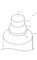
- FIG. 2 is a perspective view of the center electrode 50 as viewed from the chip 54 side.
- the center electrode 50 has a chip 54 bonded to an electrode base material 52 via a melting portion 55.
- the chip 54 is formed in a cylindrical shape.
- the electrode base material 52 has a cylindrical tip 52a protruding at the tip.
- the distal end portion 52 a is set to have a slightly larger outer diameter than the outer diameter of the tip 54.
- a melting portion 55 is formed between the entire circumference of the bottom surface and side surface of the chip 54 and the tip portion 52a. The melted portion 55 is formed by laser light irradiation. *
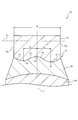
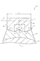
- FIG. 3 is a cross-sectional view including the central axis O of the first electrode (center electrode 50). 3, illustration of a part of the central electrode 50 in the axial direction is omitted (the illustration of part of the axial direction is the same in FIGS. 4 to 9).
- the melting portion 55 is a portion where the electrode base material 52 (tip portion 52 a) and the tip 54 are melted together, and is provided across the side surfaces 54 a and 54 a of the tip 54.
- the interface 81 between the melting portion 55 and the chip 54 includes a first portion 82, a second portion 83, and a bottom point 84 on one side (left side in FIG. 3) with the central axis O as a boundary.
- a first portion 86, a second portion 87, and a bottom point 88 are provided on one side (the right side in FIG. 3) as a boundary. *
- the second portion 83, the first portion 82, the first portion 86, and the second portion 87 are connected in order (from left to right in FIG. 3).
- the first portion 82 and the first portion 86 are connected at a local maximum point 85.
- the local maximum point 85 is located on the central axis O.
- the local maximum point 85 is a point closest to the virtual straight line 80 in the direction parallel to the central axis O among the first portion 82 and the first portion 86. *
- the first portion 82 is a portion sandwiched between the local maximum point 85 and the bottom point 84 and gradually moves away from the virtual straight line 80 in a direction parallel to the central axis O as the distance from the central axis O increases.
- the first portion 82 has an inflection point.
- the virtual straight line 80 is a virtual straight line orthogonal to the central axis O, and is provided at an arbitrary position on the second electrode (ground electrode 30) side (upper side in FIG. 3) than the interface 81. *
- the second portion 83 is a portion sandwiched between the bottom point 84 and the side surface 54 a of the chip 54, and gradually approaches the virtual straight line 80 in a direction parallel to the central axis O as the distance from the central axis O increases.
- the second portion 83 exists outside the first portion 82 in the direction orthogonal to the central axis O (hereinafter referred to as “axis-perpendicular direction”).
- axis-perpendicular direction The position of the second portion 83 farthest from the central axis O intersects the side surface 54 a of the chip 54.
- the bottom point 84 is a point connecting the first portion 82 and the second portion 83.
- the bottom point 84 is farthest from the imaginary straight line 80 in the direction parallel to the central axis O among the first portion 82 and the second portion 83.
- the first portion 86 is a portion sandwiched between the local maximum point 85 and the bottom point 88 and gradually moves away from the virtual straight line 80 in a direction parallel to the central axis O as the distance from the central axis O increases.
- the first portion 86 has an inflection point.
- the second portion 87 is a portion sandwiched between the bottom point 88 and the side surface 54 a of the chip 54, and gradually approaches the virtual straight line 80 in a direction parallel to the central axis O as the distance from the central axis O increases.
- the second portion 87 exists outside the first portion 86 in the direction perpendicular to the axis.
- the position of the second portion 87 farthest from the central axis O intersects the side surface 54 a of the chip 54. *
- a bottom point 88 is a point connecting the first portion 86 and the second portion 87.
- the bottom point 88 is farthest from the virtual straight line 80 in the direction parallel to the central axis O among the first portion 86 and the second portion 87.
- the electrode base material 52 of the center electrode 50 and the chip 54 are joined by, for example, the following method. First, the chip 54 is placed on the electrode base material 52 and pressed. Next, in a state where the tip 54 is pressed against the electrode base material 52, the tip 54 is rotated around the central axis. Then, the center axis of the chip 54 and the beam axis of the laser beam are crossed so that the laser beam is irradiated near the boundary between the chip 54 and the electrode base material 52. As a result, the melting portion 55 is formed on the entire circumference of the tip 54 and the electrode base material 52. *
- the melting part 55 has a thermal expansion coefficient larger than that of the chip 54. Accordingly, if the tip 54 and the melting portion 55 are thermally expanded in the direction perpendicular to the axis when the spark plug 10 is used, the tip 54 becomes a barrier across the first portion 82 due to the difference in thermal expansion coefficient, and the melting portion 55 is expanded. regulate. Although the second portion 83 of the melting portion 55 expands outward in the direction perpendicular to the axis with respect to the first portion 82, the size of the second portion 83 can be shortened by the amount of the first portion 82. The amount of thermal expansion in the direction perpendicular to the axis 83 can be reduced.
- the first portion 86 functions in the same manner as the first portion 82. *
- the base 84 When the length (linear distance) of the interface 81 in the direction orthogonal to the central axis O (perpendicular to the axis) is W and the distance between the base 84 and the central axis O is X1, the base 84 is 0.1. It exists in the position which satisfy
- the bottom point 84 exists at a position satisfying X1 / W ⁇ 0.1, so that the first portion 82 is relatively short, so that the barrier effect of the first portion 82 is poor, and the expansion of the melting portion 55 is restricted.
- the function of the 1st part 82 to perform falls.
- the bottom point 84 is present at a position satisfying X1 / W> 0.4, the first portion 82 is relatively long, so that the chip 54 serving as a barrier across the first portion 82 resists expansion of the melting portion 55. This makes it difficult to peel off the chip 54 from the melting portion 55.
- the bottom point 84 exists at a position satisfying 0.1 ⁇ X1 / W ⁇ 0.4, these problems can be solved. There is a similar relationship with respect to the bottom point 88. *
- the first portion 82, the second portion 83, and the bottom point 84 exist on one side (left side in FIG. 3) with the central axis O as a set, and the first portion 86, the second portion 87, and the bottom point 88. Exist on one side (right side in FIG. 3) with the central axis O as a boundary. Thereby, since the thermal stress on both sides of the interface 81 across the central axis O can be suppressed, the chip 54 can be made more difficult to peel off. *
- the first portions 82 and 86 have inflection points, the first portions 82 and 86 in the vicinity of the bottom points 84 and 88 and the local maximum point 85 are compared with the case where the first portion has no inflection points.
- the curvature and the inclination of the first portions 82 and 86 with respect to the central axis O in the vicinity of the bottom points 84 and 88 and the maximum point 85 can be reduced.
- the load due to the difference in thermal expansion between the tip 54 and the melting portion 55 can be prevented from being concentrated near the bottom points 84 and 88 and the maximum point 85. Therefore, it is possible to suppress the load near the bottom points 84 and 88 and the maximum point 85 and to prevent the interface 81 from cracking.
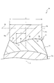
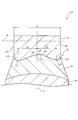
- FIG. 4 is a cross-sectional view including the central axis O of the first electrode (center electrode 90) in the second embodiment.
- the center electrode 90 is disposed on the spark plug 10 in place of the center electrode 50 described in the first embodiment (the same applies to the third and subsequent embodiments).
- the interface 91 between the melting portion 55 and the chip 54 includes a first portion 92, a second portion 93, and a bottom point 94 on one side (left side in FIG. 4) with the central axis O as a boundary. *
- a second portion 93, a first portion 92, a second portion 95, and a first portion 96 are connected in order (from left to right in FIG. 4).
- the first portion 92 is a portion sandwiched between the central axis O and the bottom point 94, and gradually moves away from the virtual straight line 80 in a direction parallel to the central axis O as the distance from the central axis O increases.
- the first portion 92 has an inflection point.
- the second portion 93 is a portion sandwiched between the bottom 94 and the side surface 54 a of the chip 54, and gradually approaches the virtual straight line 80 in a direction parallel to the central axis O as the distance from the central axis O increases.
- the second portion 93 exists outside the first portion 92 in the direction perpendicular to the axis. The position of the second portion 93 farthest from the central axis O intersects the side surface 54 a of the chip 54. *
- the bottom point 94 is a point connecting the first portion 92 and the second portion 93.
- the bottom point 94 is farthest from the imaginary straight line 80 in the direction parallel to the central axis O among the first portion 92 and the second portion 93.
- the bottom point 94 satisfies 0.1 ⁇ X / W ⁇ 0.4. It exists in the position to satisfy.
- the second portion 95 is a portion sandwiched between the central axis O and the maximum point 97, and gradually approaches the virtual straight line 80 in a direction parallel to the central axis O as the distance from the central axis O increases.
- the first portion 96 is a portion sandwiched between the maximum point 97 and the side surface 54 a of the chip 54, and gradually moves away from the virtual straight line 80 in a direction parallel to the central axis O as the distance from the central axis O increases.
- the maximum point 97 is at a position closest to the virtual straight line 80 in the direction parallel to the central axis O in the second portion 95 and the first portion 96. *
- the tip 54 and the melting portion 55 expand in the direction perpendicular to the axis, the tip 54 becomes a barrier across the first portion 92 due to the difference in thermal expansion coefficient.
- the expansion of the melting part 55 is regulated. Since the size of the second portion 93 can be shortened by the amount corresponding to the first portion 92, the amount of thermal expansion in the direction perpendicular to the axis of the second portion 93 relative to the chip 54 can be reduced. As a result, cracks and oxide scale can hardly be generated in the second portion 93 that intersects the side surface 54 a of the chip 54, so that the chip 54 can be hardly peeled off from the melting portion 55.
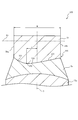
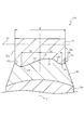
- FIG. 5 is a cross-sectional view including the central axis O of the first electrode (center electrode 100) in the third embodiment.
- the interface 101 between the melting portion 55 and the chip 54 includes a first portion 102, a second portion 103, and a bottom point 104 on one side (left side in FIG. 5) with the central axis O as a boundary.
- the second portion 103, the first portion 102, and the second portion 105 are connected in order (from left to right in FIG. 5).
- the first portion 102 is a portion sandwiched between the central axis O and the bottom point 104, and gradually moves away from the virtual straight line 80 in a direction parallel to the central axis O as the distance from the central axis O increases.
- the second portion 103 is a portion sandwiched between the bottom point 104 and the side surface 54 a of the chip 54, and gradually approaches the virtual straight line 80 in a direction parallel to the central axis O as the distance from the central axis O increases.
- the second portion 103 exists outside the first portion 102 in the direction perpendicular to the axis. The position of the second portion 103 farthest from the central axis O intersects the side surface 54 a of the chip 54. *
- the bottom point 104 is a point connecting the first portion 102 and the second portion 103.
- the bottom point 104 is farthest from the imaginary straight line 80 in a direction parallel to the central axis O among the first portion 102 and the second portion 103.
- the bottom point 104 satisfies 0.1 ⁇ X / W ⁇ 0.4. It exists in the position to satisfy.
- the second portion 105 is a portion sandwiched between the central axis O and the side surface 54 a of the chip 54, and gradually approaches the virtual straight line 80 in a direction parallel to the central axis O as the distance from the central axis O increases.
- the tip 54 and the melting portion 55 expand in the direction perpendicular to the axis, the tip 54 becomes a barrier across the first portion 102 due to the difference in thermal expansion coefficient. Therefore, the expansion of the melting part 55 is regulated. Since the amount of thermal expansion in the direction perpendicular to the axis of the second portion 103 can be reduced, cracks and oxide scale can be hardly generated in the second portion 103.
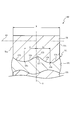
- FIG. 6 is a cross-sectional view including the central axis O of the first electrode (center electrode 110) in the fourth embodiment. *
- the interface 111 between the melting portion 55 and the chip 54 includes a first portion 112, a second portion 113, and a bottom point 114 on one side (left side in FIG. 6) with the central axis O as a boundary.
- a first portion 116, a second portion 117, and a bottom point 118 are provided on one side (the right side in FIG. 6) as a boundary.
- the second portion 113, the first portion 112, the first portion 116, and the second portion 117 are connected in order (from left to right in FIG. 6).
- the first portion 112 and the first portion 116 are connected at a local maximum point 115.
- the maximum point 115 is located on the central axis O. *
- the first portion 112 is a portion sandwiched between the local maximum point 115 and the bottom point 114, and gradually moves away from the virtual straight line 80 in a direction parallel to the central axis O as the distance from the central axis O increases.
- the first portion 112 has an inflection point.
- the second portion 113 is a portion sandwiched between the bottom point 114 and the side surface 54 a of the chip 54, and gradually approaches the virtual straight line 80 in a direction parallel to the central axis O as the distance from the central axis O increases.
- the bottom point 114 is farthest from the imaginary straight line 80 in the direction parallel to the central axis O among the first portion 112 and the second portion 113. *
- the first portion 116 is a portion sandwiched between the local maximum point 115 and the bottom point 118, and gradually moves away from the virtual straight line 80 in a direction parallel to the central axis O as the distance from the central axis O increases.
- the first portion 116 has an inflection point.
- the second portion 117 is a portion sandwiched between the bottom point 118 and the side surface 54 a of the chip 54, and gradually approaches the virtual straight line 80 in a direction parallel to the central axis O as the distance from the central axis O increases.
- the bottom point 118 is farthest from the imaginary straight line 80 in the direction parallel to the central axis O among the first portion 116 and the second portion 117.
- the bottom point 114 satisfies 0.1 ⁇ X1 / W ⁇ 0.4. It exists in the position to satisfy. Further, when the distance between the base point 118 and the central axis O is X2, the base point 118 exists at a position satisfying 0.1 ⁇ X2 / W ⁇ 0.4. According to 4th Embodiment, since it is comprised similarly to 1st Embodiment, the effect similar to 1st Embodiment is obtained.
- FIG. 7 is a cross-sectional view including the central axis O of the first electrode (center electrode 120) in the fifth embodiment. *
- the interface 121 between the melting portion 55 and the chip 54 includes a first portion 122, a second portion 123, and a bottom point 124 on one side (left side in FIG. 7) with the central axis O as a boundary.
- a first portion 126, a second portion 128, and a bottom point 119 are provided on one side (the right side in FIG. 7) as a boundary.
- the second portion 123, the first portion 122, the first portion 126, the second portion 125, the first portion 126, and the second portion 128 are connected in order (from left to right in FIG. 7). *
- the first portion 122 is a portion sandwiched between the central axis O and the bottom point 124, and gradually moves away from the virtual straight line 80 in a direction parallel to the central axis O as the distance from the central axis O increases.
- the first portion 122 has an inflection point.
- the second portion 123 is a portion sandwiched between the bottom point 124 and the side surface 54 a of the chip 54, and gradually approaches the virtual straight line 80 in a direction parallel to the central axis O as the distance from the central axis O increases.
- the bottom point 124 is farthest from the imaginary straight line 80 in a direction parallel to the central axis O in the first portion 122 and the second portion 123.
- the second portion 125 is a portion sandwiched between the central axis O and the maximum point 127, and gradually approaches the virtual straight line 80 in a direction parallel to the central axis O as the distance from the central axis O increases.
- the first portion 126 is a portion sandwiched between the maximum point 127 and the bottom point 129, and gradually moves away from the virtual straight line 80 in a direction parallel to the central axis O as the distance from the central axis O increases.
- the first portion 126 has an inflection point.
- the second portion 128 is a portion sandwiched between the bottom point 129 and the side surface 54 a of the chip 54, and gradually approaches the virtual straight line 80 in a direction parallel to the central axis O as the distance from the central axis O increases.
- the bottom point 129 is farthest from the imaginary straight line 80 in the direction parallel to the central axis O among the first portion 126 and the second portion 128.
- the base point 124 When the length (linear distance) of the interface 121 in the direction perpendicular to the axis is W and the distance between the base point 124 and the central axis O is X1, the base point 124 satisfies 0.1 ⁇ X1 / W ⁇ 0.4. It exists in the position to satisfy. Further, when the distance between the base point 129 and the central axis O is X2, the base point 129 exists at a position satisfying 0.1 ⁇ X2 / W ⁇ 0.4. According to the fifth embodiment, since the configuration is the same as that of the first embodiment, the same effect as that of the first embodiment can be obtained. *
- FIG. 8 is a cross-sectional view including the central axis O of the first electrode (center electrode 130) in the sixth embodiment. *
- the interface 131 between the melting portion 55 and the chip 54 includes a first portion 132, a second portion 133, and a bottom point 134 on one side (left side in FIG. 8) with the central axis O as a boundary.
- a first part 136, a second part 138, and a bottom point 139 are provided on one side (the right side in FIG. 8) as a boundary.
- the second portion 133, the first portion 132, the second portion 135, the first portion 136, and the second portion 138 are connected in order (from left to right in FIG. 8). *
- the first portion 132 is a portion sandwiched between the central axis O and the bottom point 134, and gradually moves away from the virtual straight line 80 in a direction parallel to the central axis O as the distance from the central axis O increases.
- the first portion 132 has an inflection point.
- the second portion 133 is a portion sandwiched between the bottom point 134 and the side surface 54 a of the chip 54, and gradually approaches the virtual straight line 80 in a direction parallel to the central axis O as the distance from the central axis O increases.
- the bottom point 134 is farthest from the imaginary straight line 80 in a direction parallel to the central axis O of the first portion 132 and the second portion 133.
- the second portion 135 is a portion sandwiched between the central axis O and the maximum point 137, and gradually approaches the virtual straight line 80 in a direction parallel to the central axis O as the distance from the central axis O increases.
- the first portion 136 is a portion sandwiched between the local maximum point 137 and the bottom point 139 and gradually moves away from the virtual straight line 80 in a direction parallel to the central axis O as the distance from the central axis O increases.
- the first portion 136 has an inflection point.
- the second portion 138 is a portion sandwiched between the bottom point 139 and the side surface 54 a of the chip 54, and gradually approaches the virtual straight line 80 in a direction parallel to the central axis O as the distance from the central axis O increases.
- the bottom point 139 is farthest from the imaginary straight line 80 in the direction parallel to the central axis O in the first portion 136 and the second portion 138.
- the base point 134 When the length (linear distance) of the interface 131 in the direction perpendicular to the axis is W and the distance between the base point 134 and the central axis O is X1, the base point 134 satisfies 0.1 ⁇ X1 / W ⁇ 0.4. It exists in the position to satisfy. Further, when the distance between the base point 139 and the central axis O is X2, the base point 139 exists at a position satisfying 0.1 ⁇ X2 / W ⁇ 0.4. According to the sixth embodiment, since it is configured in the same manner as in the first embodiment, the same operational effects as in the first embodiment can be obtained. *
- FIG. 9 is a cross-sectional view including the central axis O of the first electrode (center electrode 140) in the seventh embodiment.
- the chip 54 is bonded to the electrode base material 141 through the melting part 150.
- the interface 151 between the melting part 150 and the chip 54 includes a first portion 152, a second portion 153, and a bottom point 154 on one side (left side in FIG. 9) with the central axis O as a boundary.
- a first portion 156, a second portion 158, and a bottom point 159 are provided on one side (the right side in FIG. 9) as a boundary.
- the second portion 153, the first portion 152, the second portion 155, the first portion 156, and the second portion 158 are connected in order (from left to right in FIG. 9). *
- the first portion 152 is a portion sandwiched between the central axis O and the bottom point 154 and gradually moves away from the virtual straight line 80 in a direction parallel to the central axis O as the distance from the central axis O increases.
- the first portion 152 has an inflection point.
- the second portion 153 is a portion sandwiched between the bottom point 154 and the side surface 54 a of the chip 54, and gradually approaches the virtual straight line 80 in a direction parallel to the central axis O as the distance from the central axis O increases.
- the bottom point 154 is farthest from the imaginary straight line 80 in the direction parallel to the central axis O in the first portion 152 and the second portion 153. *
- the second portion 155 is a portion sandwiched between the central axis O and the maximum point 157, and gradually approaches the virtual straight line 80 in a direction parallel to the central axis O as the distance from the central axis O increases.
- the first portion 156 is a portion sandwiched between the local maximum point 157 and the bottom point 159, and gradually moves away from the virtual straight line 80 in a direction parallel to the central axis O as the distance from the central axis O increases.
- the first portion 156 has an inflection point.
- the second portion 158 is a portion sandwiched between the bottom point 159 and the side surface 54 a of the chip 54, and gradually approaches the virtual straight line 80 in a direction parallel to the central axis O as the distance from the central axis O increases.
- the bottom point 159 is farthest from the imaginary straight line 80 in the direction parallel to the central axis O in the first portion 156 and the second portion 158.
- the bottom point 154 satisfies 0.1 ⁇ X1 / W ⁇ 0.4. It exists in the position to satisfy. Further, when the distance between the base point 159 and the central axis O is X2, the base point 159 exists at a position satisfying 0.1 ⁇ X2 / W ⁇ 0.4. According to the seventh embodiment, since the configuration is the same as that of the first embodiment, the same effect as that of the first embodiment can be obtained.
- the tip was made of a columnar iridium alloy, and one having a diameter of 0.55 mm and a height of 0.65 mm and one having a diameter of 0.8 mm and a height of 0.6 mm were used.
- the electrode base material was made of nickel alloy (Inconel 600) (registered trademark).
- the tip of the electrode base material to which the chip is joined was 0.85 mm in the case of a chip having a diameter of 0.55 mm, and 1.1 mm in the case of a chip having a diameter of 0.8 mm. *
- center electrodes were obtained by adjusting the output of laser welding, the irradiation position of the laser beam, and the irradiation pattern.
- a cross section of the central electrode including the central axis O was observed nondestructively using an X-ray fluoroscopy device, and samples with or without a bottom at the interface between the tip and the melted part were randomly extracted.
- Various spark plugs were obtained by assembling the extracted center electrode. Analysis of the melted portion formed on the center electrode showed that the noble metal component of the tip was contained in an amount of 25 to 35 wt%.
- the length L of the oxide scale was measured for each cross section on one side with the central axis as the boundary.
- the length L was divided by 0.5 W (chip radius), and the ratio (%) of the oxide scale to the chip radius was calculated.
- the ratio of the oxide scale was less than 50%, it was judged as “excellent ( ⁇ )”, 50% or more and less than 80% as “good ( ⁇ )”, and 80% or more as “poor ( ⁇ )”.
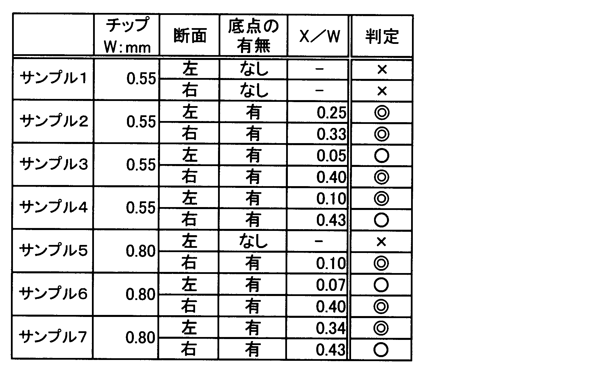
- Table 1 is a list of test results of samples 1 to 7.
- a section on one side with the central axis as a boundary (a cross section existing on the left and right sides of the central axis) is described as “left” and “right” in the “cross section” column.
- the ratio of the oxide scale at the interface can be made less than 80% (determination is ⁇ or ⁇ ).
- the range of X / W at this time was 0.1 ⁇ X / W ⁇ 0.4 when rounded off to the second decimal place.
- the ratio of the oxide scale at the interface can be made less than 50% (determination is ⁇ ).
- the present invention has been described above based on the embodiments. However, the present invention is not limited to the above embodiments, and various improvements and modifications can be made without departing from the spirit of the present invention. It can be easily guessed. For example, the shapes, dimensions, materials, and the like of the electrode base material 52 and the chip 54 are examples and can be set as appropriate. *
- the present invention is not necessarily limited thereto.
- the shape of the chip 54 can be appropriately set, such as an elliptical column shape or a polygonal column shape.
- the present invention is not necessarily limited thereto.
- the above-described embodiments can be applied to the manufacture of a spark plug that does not incorporate the resistor 70.
- the resistor 70 and the conductive seal 72 may be omitted, and the center electrode 50 and the terminal fitting 60 may be joined by the conductive seal 71.
- the first portion serves as a barrier that regulates thermal expansion at least in that portion. This is because it can be suppressed.
Landscapes
- Engineering & Computer Science (AREA)
- Manufacturing & Machinery (AREA)
- Spark Plugs (AREA)
Abstract
チップを剥離し難くできるスパークプラグを提供すること。チップの中心軸を含む断面において、溶融部とチップとの界面は、中心軸に直交すると共に界面よりも第2電極側に位置する仮想直線から、中心軸から離れるにつれて中心軸と平行な方向へ次第に離れる第1部分と、中心軸と平行な方向において、中心軸から離れるにつれて仮想直線へ次第に近づく第2部分と、第1部分と第2部分とを繋ぐ底点とを備える。底点は、第1部分および第2部分のうち、中心軸と平行な方向において仮想直線から最も離れた位置である。第1部分、第2部分および底点は、全てが、断面のうち中心軸を境目とする片側に少なくとも存在し、中心軸に直交する方向の界面の長さをWとし、底点と中心軸との距離をXとしたときに、底点は0.1≦X/W≦0.4を満たす位置に存在する。
Description
本発明はスパークプラグに関し、特にチップを剥離し難くできるスパークプラグに関するものである。
貴金属を含有するチップと電極母材とが溶融部を介して接合された第1電極と、チップと火花ギャップを介して対向する第2電極とを備えるスパークプラグが知られている(例えば特許文献1)。スパークプラグは火花ギャップ間に放電を生じさせ、第1電極と第2電極とが曝された混合気に点火することにより火炎核を形成する。チップと溶融部とは熱膨張率が異なるので、チップと溶融部との界面に熱応力が発生する。
しかしながら上述した従来の技術では、熱応力によってチップと溶融部との界面にクラック及び酸化スケールが発生し易いので、クラックや酸化スケールが過度に進行すると、チップが溶融部から剥離し脱落するおそれがある。
本発明は上述した問題点を解決するためになされたものであり、チップを剥離し難くできるスパークプラグを提供することを目的としている。
この目的を達成するために請求項1記載のスパークプラグによれば、第1電極は、貴金属を含有する柱状のチップと、チップを支持する電極母材と、チップ及び電極母材が溶け合ってなる溶融部とを備えている。第2電極はチップと火花ギャップを介して対向する。チップの中心軸を含む断面において、溶融部とチップとの界面は、中心軸に直交すると共に界面よりも第2電極側に位置する仮想直線から、中心軸から離れるにつれて中心軸と平行な方向へ次第に離れる第1部分と、中心軸と平行な方向において、中心軸から離れるにつれて仮想直線へ次第に近づく第2部分と、第1部分と第2部分とを繋ぐ底点とを備えている。底点は、第1部分および第2部分のうち、中心軸と平行な方向において仮想直線から最も離れた位置である。
第1部分、第2部分および底点は、全てが、断面のうち中心軸を境目とする片側に少なくとも存在し、中心軸に直交する方向の界面の長さをWとし、底点と中心軸との距離をXとしたときに、底点は0.1≦X/W≦0.4を満たす位置に存在する。第1部分は、中心軸から離れるにつれて中心軸と平行な方向へ次第に離れるので、中心軸と直交する方向におけるチップに対する溶融部の熱膨張を規制する。少なくとも片側の断面において、中心軸と直交する方向におけるチップに対する第2部分の熱膨張量を小さくできるので、熱応力を緩和してチップを剥離し難くできる効果がある。
請求項2記載のスパークプラグによれば、底点、第1部分および第2部分は、それらを1組として、中心軸を境目とする断面の両側にそれぞれ存在する。中心軸を挟んで界面の両側の熱応力を抑制できるので、請求項1の効果に加え、チップをより剥離し難くできる効果がある。
以下、本発明の好ましい実施形態について添付図面を参照して説明する。図1は本発明の第1実施の形態におけるスパークプラグ10の中心軸Oを含む面で切断した断面図である。図1では、紙面下側をスパークプラグ10の先端側、紙面上側をスパークプラグ10の後端側という。図1に示すようにスパークプラグ10は、主体金具20、接地電極30、絶縁体40、中心電極50及び端子金具60を備えている。
主体金具20は、内燃機関のねじ穴(図示せず)に固定される略円筒状の部材であり、中心軸Oに沿って貫通する貫通孔21が形成されている。主体金具20は導電性を有する金属材料(例えば低炭素鋼等)によって形成されている。主体金具20は、径方向の外側へ鍔状に張り出す座部22と、座部22より先端側の外周面に形成されたねじ部23とを備えている。
座部22とねじ部23との間に環状のガスケット24が嵌め込まれている。ガスケット24は、内燃機関のねじ穴にねじ部23が嵌められたときに、主体金具20と内燃機関(エンジンヘッド)との隙間を封止する。
接地電極30は、主体金具20の先端に接合される金属製(例えばニッケル基合金製)の電極母材31と、電極母材31の先端に接合されるチップ32とを備えている。電極母材31は、中心軸Oと交わるように中心軸Oへ向かって屈曲する棒状の部材である。チップ32は、白金、イリジウム、ルテニウム、ロジウム等の貴金属またはこれらを主成分とする合金によって形成される板状の部材であり、レーザ溶接等によって中心軸Oと交わる位置に接合されている。
絶縁体40は、機械的特性や高温下の絶縁性に優れるアルミナ等により形成された略円筒状の部材であり、中心軸Oに沿って貫通する軸孔41が形成されている。絶縁体40は、主体金具20の貫通孔21に挿入され、外周に主体金具20が固定されている。絶縁体40は、先端および後端が、主体金具20の貫通孔21からそれぞれ露出している。
軸孔41は、絶縁体40の先端側に位置する第1孔部42と、第1孔部42の後端に連なり後端側へ向かうにつれて拡径する段部43と、段部43の後端側に位置する第2孔部44とを備えている。第2孔部44は、内径が、第1孔部42の内径より大きく設定されている。
中心電極50は、有底筒状に形成された電極母材52の内部に、電極母材52よりも熱伝導性に優れる芯材53を埋設した棒状の電極である。芯材53は銅または銅を主成分とする合金で形成されている。電極母材52は大部分が第1孔部42内に位置する。電極母材52は先端が第1孔部42から露出し、先端にチップ54がレーザ溶接等によって接合されている。
チップ54は、白金、イリジウム、ルテニウム、ロジウム等の貴金属またはこれらを主成分とする合金によって形成される柱状の部材であり、火花ギャップを介して接地電極30のチップ32と対向する。本実施の形態では、中心電極50を第1電極とし、接地電極30を第2電極とする。
端子金具60は、高圧ケーブル(図示せず)が接続される棒状の部材であり、導電性を有する金属材料(例えば低炭素鋼等)によって形成されている。端子金具60の先端側は絶縁体40の軸孔41内に配置される。
抵抗体70は、スパーク時に発生する電波ノイズを抑えるための部材であり、端子金具60と中心電極50との間の第2孔部44内に配置されている。抵抗体70と中心電極50との間、抵抗体70と端子金具60との間に、導電性を有する導電性シール71,72がそれぞれ配置される。導電性シール71は抵抗体70と中心電極50とにそれぞれ接触し、導電性シール72は抵抗体70と端子金具60とにそれぞれ接触する。この結果、中心電極50と端子金具60とは、抵抗体70と導電性シール71,72とを介して電気的に接続される。
スパークプラグ10は、例えば、以下のような方法によって製造される。まず、絶縁体40の第2孔部44から中心電極50を挿入する。中心電極50は、電極母材52の先端にチップ54が溶接されている。中心電極50は段部43に後端部51が支持され、先端部が軸孔41の先端から外部に露出するように配置される。
次に、導電性シール71の原料粉末を第2孔部44から入れて、後端部51の周囲および後端側に充填する。圧縮用棒材(図示せず)を用いて、第2孔部44に充填した導電性シール71の原料粉末を予備圧縮する。成形された導電性シール71の原料粉末の成形体の上に、抵抗体70の原料粉末を充填する。圧縮用棒材(図示せず)を用いて、第2孔部44に充填した抵抗体70の原料粉末を予備圧縮する。次いで、抵抗体70の原料粉末の上に、導電性シール72の原料粉末を充填する。圧縮用棒材(図示せず)を用いて、第2孔部44に充填した導電性シール72の原料粉末を予備圧縮する。
次に、軸孔41の後端側から端子金具60の先端部61を挿入して、先端部61が導電性シール72の原料粉末に接触するように端子金具60を配置する。次いで、例えば各原料粉末に含まれるガラス成分の軟化点より高い温度まで加熱しつつ、端子金具60の後端側に設けられた鍔部62の先端面が絶縁体40の後端面に当接するまで端子金具60を圧入して、端子金具60の先端部61によって導電性シール71、抵抗体70及び導電性シール72の原料粉末に軸方向の荷重を加える。この結果、各原料粉末が圧縮・焼結され、絶縁体40の内部に導電性シール71、抵抗体70及び導電性シール72が形成される。
次に、予め接地電極30が接合された主体金具20を絶縁体40の外周に組み付ける。その後、接地電極30の電極母材31にチップ32を溶接し、接地電極30のチップ32が中心電極50のチップ54と軸方向に対向するように電極母材31を屈曲して、スパークプラグ10を得る。
図2は、チップ54側から見た中心電極50の斜視図である。図2に示すように中心電極50は、電極母材52に溶融部55を介してチップ54が接合されている。チップ54は円柱状に形成されている。電極母材52は先端に円柱状の先端部52aが突出する。先端部52aは、外径が、チップ54の外径より少し大きく設定されている。チップ54の底面および側面の全周と先端部52aとの間に溶融部55が形成されている。溶融部55はレーザ光の照射により形成される。
図3は第1電極(中心電極50)の中心軸Oを含む断面図である。図3では中心電極50の軸方向の一部の図示が省略されている(軸方向の一部の図示の省略は図4から図9において同じ)。溶融部55は、電極母材52(先端部52a)及びチップ54が溶け合ってなる部位であり、チップ54の側面54a,54aに亘って設けられている。図3において、溶融部55とチップ54との界面81は、中心軸Oを境目とする片側(図3左側)に第1部分82、第2部分83及び底点84を備え、中心軸Oを境目とする片側(図3右側)に第1部分86、第2部分87及び底点88を備えている。
界面81は、第2部分83、第1部分82、第1部分86及び第2部分87が順に(図3左から右へ)連接されている。第1部分82と第1部分86とは極大点85で接続される。本実施の形態では、極大点85は中心軸O上に位置する。極大点85は、第1部分82及び第1部分86のうち、中心軸Oと平行な方向において、仮想直線80に最も近い点である。
第1部分82は、極大点85と底点84とに挟まれた部分であり、中心軸Oから離れるにつれて、中心軸Oと平行な方向へ仮想直線80から次第に離れる。第1部分82は変曲点を有している。仮想直線80は中心軸Oに直交する仮想の直線であり、界面81よりも第2電極(接地電極30)側(図3上側)の任意の位置に設けられる。
第2部分83は、底点84とチップ54の側面54aとに挟まれた部分であり、中心軸Oから離れるにつれて、中心軸Oと平行な方向へ、仮想直線80へ次第に近づく。第2部分83は、第1部分82よりも、中心軸Oと直交する方向(以下「軸直角方向」と称す)の外側に存在する。第2部分83は、中心軸Oから最も離れた位置がチップ54の側面
54aに交わる。
54aに交わる。
底点84は、第1部分82と第2部分83とを繋ぐ点である。底点84は、第1部分82及び第2部分83のうち、中心軸Oと平行な方向において仮想直線80から最も離れている。
第1部分86は、極大点85と底点88とに挟まれた部分であり、中心軸Oから離れるにつれて、中心軸Oと平行な方向へ仮想直線80から次第に離れる。第1部分86は変曲点を有している。第2部分87は、底点88とチップ54の側面54aとに挟まれた部分であり、中心軸Oから離れるにつれて、中心軸Oと平行な方向へ、仮想直線80へ次第に近づく。第2部分87は、第1部分86よりも軸直角方向の外側に存在する。第2部分87は、中心軸Oから最も離れた位置がチップ54の側面54aに交わる。
底点88は、第1部分86と第2部分87とを繋ぐ点である。底点88は、第1部分86及び第2部分87のうち、中心軸Oと平行な方向において仮想直線80から最も離れている。
中心電極50の電極母材52とチップ54との接合は、例えば以下の方法によって行われる。まず、電極母材52にチップ54を載置し、押さえつける。次に、電極母材52にチップ54を押さえつけた状態で、チップ54の中心軸を中心に回転させる。そして、チップ54の中心軸とレーザ光のビーム軸とを交差させて、チップ54と電極母材52との境界付近にレーザ光を照射する。これにより、チップ54及び電極母材52の全周に溶融部55が形成される。
レーザ溶接の出力、チップ54及び電極母材52の回転数、レーザ光の照射位置および照射パターンを適宜調整することによって、溶融部55は中心軸付近に熱が蓄積される。その結果、溶融部55の中心軸O近傍が軸方向に膨らむので、溶融部55とチップ54との界面81に第1部分82,86、第2部分83,87及び底点84,88が形成される。
溶融部55は、熱膨張率が、チップ54の熱膨張率より大きい。従って、スパークプラグ10の使用時に、チップ54及び溶融部55が軸直角方向に熱膨張すると、熱膨張率の差によって第1部分82を挟んでチップ54が障壁になり、溶融部55の膨張を規制する。溶融部55の第2部分83は第1部分82に対して軸直角方向の外側に膨張するが、第1部分82の分だけ第2部分83の寸法を短くできるので、チップ54に対する第2部分83の軸直角方向の熱膨張量を小さくできる。その結果、チップ54の側面54aに交わる第2部分83の熱応力を緩和できるので、第2部分83が開放されるのを抑制し、クラック及び酸化スケールを発生し難くできる。よって、溶融部55からチップ54を剥離し難くできる。第1部分86も第1部分82と同様に機能する。
中心軸Oに直交する方向(軸直角方向)の界面81の長さ(直線距離)をWとし、底点84と中心軸Oとの距離をX1としたときに、底点84は0.1≦X1/W≦0.4を満たす位置に存在する。また、底点88と中心軸Oとの距離をX2としたときに、底点88は0.1≦X2/W≦0.4を満たす位置に存在する。これにより、溶融部55からチップ54を剥離し難くできる。
即ち、底点84がX1/W<0.1を満たす位置に存在すると、第1部分82が相対的に短いので、第1部分82の障壁の効果が乏しくなり、溶融部55の膨張を規制する第1部分82の機能が低下する。底点84がX1/W>0.4を満たす位置に存在すると、第1部分82が相対的に長いので、第1部分82を挟んで障壁となるチップ54が、溶融部55の膨張に抗し難くなり、溶融部55からチップ54が剥離し易くなる。0.1≦X1/W≦0.4を満たす位置に底点84を存在させると、これらの問題を解決できる。底点88についても同様の関係がある。
第1部分82、第2部分83及び底点84は、それらを1組として中心軸Oを境目とする片側(図3左側)に存在し、第1部分86、第2部分87及び底点88は、それらを1組として中心軸Oを境目とする片側(図3右側)に存在する。これにより、中心軸Oを挟んで界面81の両側の熱応力を抑制できるので、チップ54をより剥離し難くできる。
第1部分82,86は変曲点を有しているので、第1部分が変曲点を有しない場合に比べて、底点84,88及び極大点85付近の第1部分82,86の曲率や、底点84,88及び極大点85付近における中心軸Oに対する第1部分82,86の傾きを小さくできる。その結果、チップ54と溶融部55との熱膨張の差による荷重を底点84,88や極大点85付近に集中させないようにできる。よって、底点84,88や極大点85付近の荷重を抑制して、界面81にクラックを生じ難くできる。
次に図4を参照して第2実施の形態について説明する。第1実施の形態では、底点84,88、第1部分82,86及び第2部分83,87が、それぞれを1組として中心軸Oを境目とする断面の両側に存在する場合について説明した。これに対し第2実施の形態では、第1部分92、第2部分93及び底点94が、中心軸Oを境目とする断面の片側に存在する場合について説明する。なお、第1実施の形態で説明した部分と同一の部分については、同一の符号を付して以下の説明を省略する。
図4は第2実施の形態における第1電極(中心電極90)の中心軸Oを含む断面図である。中心電極90は、第1実施の形態で説明した中心電極50に代えて、スパークプラグ10に配置される(第3実施の形態以後も同じ)。図4において、溶融部55とチップ54との界面91は、中心軸Oを境目とする片側(図4左側)に第1部分92、第2部分93及び底点94を備えている。
界面91は、第2部分93、第1部分92、第2部分95及び第1部分96が順に(図4左から右へ)連接されている。第1部分92は、中心軸Oと底点94とに挟まれた部分であり、中心軸Oから離れるにつれて、中心軸Oと平行な方向へ仮想直線80から次第に離れる。第1部分92は変曲点を有している。第2部分93は、底点94とチップ54の側面54aとに挟まれた部分であり、中心軸Oから離れるにつれて、中心軸Oと平行な方向へ、仮想直線80へ次第に近づく。第2部分93は、第1部分92よりも、軸直角方向の外側に存在する。第2部分93は、中心軸Oから最も離れた位置がチップ54の側面54aに交わる。
底点94は、第1部分92と第2部分93とを繋ぐ点である。底点94は、第1部分92及び第2部分93のうち、中心軸Oと平行な方向において仮想直線80から最も離れている。軸直角方向の界面91の長さ(直線距離)をWとし、底点94と中心軸Oとの距離をXとしたときに、底点94は0.1≦X/W≦0.4を満たす位置に存在する。
第2部分95は、中心軸Oと極大点97とに挟まれた部分であり、中心軸Oから離れるにつれて、中心軸Oと平行な方向へ仮想直線80に次第に近づく。第1部分96は、極大点97とチップ54の側面54aとに挟まれた部分であり、中心軸Oから離れるにつれて、中心軸Oと平行な方向へ、仮想直線80から次第に離れる。極大点97は、第2部分95及び第1部分96のうち、中心軸Oと平行な方向において仮想直線80に最も近い位置にある。
第2実施の形態によれば、第1実施の形態と同様に、チップ54及び溶融部55が軸直角方向に膨張すると、熱膨張率の差によって第1部分92を挟んでチップ54が障壁になり、溶融部55の膨張を規制する。第1部分92の分だけ第2部分93の寸法を短くできるので、チップ54に対する第2部分93の軸直角方向の熱膨張量を小さくできる。その結果、チップ54の側面54aに交わる第2部分93にクラック及び酸化スケールを発生し難くできるので、溶融部55からチップ54を剥離し難くできる。
次に図5を参照して第3実施の形態について説明する。なお、第1実施の形態で説明した部分と同一の部分については、同一の符号を付して以下の説明を省略する。図5は第3実施の形態における第1電極(中心電極100)の中心軸Oを含む断面図である。図5において、溶融部55とチップ54との界面101は、中心軸Oを境目とする片側(図5左側)に第1部分102、第2部分103及び底点104を備えている。
界面101は、第2部分103、第1部分102及び第2部分105が順に(図5左から右へ)連接されている。第1部分102は、中心軸Oと底点104とに挟まれた部分であり、中心軸Oから離れるにつれて、中心軸Oと平行な方向へ仮想直線80から次第に離れる。第2部分103は、底点104とチップ54の側面54aとに挟まれた部分であり、中心軸Oから離れるにつれて、中心軸Oと平行な方向へ、仮想直線80へ次第に近づく。第2部分103は、第1部分102よりも、軸直角方向の外側に存在する。第2部分103は、中心軸Oから最も離れた位置がチップ54の側面54aに交わる。
底点104は、第1部分102と第2部分103とを繋ぐ点である。底点104は、第1部分102及び第2部分103のうち、中心軸Oと平行な方向において仮想直線80から最も離れている。軸直角方向の界面101の長さ(直線距離)をWとし、底点104と中心軸Oとの距離をXとしたときに、底点104は0.1≦X/W≦0.4を満たす位置に存在する。
第2部分105は、中心軸Oとチップ54の側面54aとに挟まれた部分であり、中心軸Oから離れるにつれて、中心軸Oと平行な方向へ仮想直線80に次第に近づく。第3実施の形態によれば、第2実施の形態と同様に、チップ54及び溶融部55が軸直角方向に膨張すると、熱膨張率の差によって第1部分102を挟んでチップ54が障壁になるので、溶融部55の膨張を規制する。第2部分103の軸直角方向の熱膨張量を小さくできるので、第2部分103にクラック及び酸化スケールを発生し難くできる。
次に図6を参照して第4実施の形態について説明する。なお、第1実施の形態で説明した部分と同一の部分については、同一の符号を付して以下の説明を省略する。図6は第4実施の形態における第1電極(中心電極110)の中心軸Oを含む断面図である。
図6において、溶融部55とチップ54との界面111は、中心軸Oを境目とする片側(図6左側)に第1部分112、第2部分113及び底点114を備え、中心軸Oを境目とする片側(図6右側)に第1部分116、第2部分117及び底点118を備えている。界面111は、第2部分113、第1部分112、第1部分116及び第2部分117が順に(図6左から右へ)連接されている。第1部分112と第1部分116とは極大点115で接続される。本実施の形態では、極大点115は中心軸O上に位置する。
第1部分112は、極大点115と底点114とに挟まれた部分であり、中心軸Oから離れるにつれて、中心軸Oと平行な方向へ仮想直線80から次第に離れる。第1部分112は変曲点を有している。第2部分113は、底点114とチップ54の側面54aとに挟まれた部分であり、中心軸Oから離れるにつれて、中心軸Oと平行な方向へ、仮想直線80へ次第に近づく。底点114は、第1部分112及び第2部分113のうち、中心軸Oと平行な方向において仮想直線80から最も離れている。
第1部分116は、極大点115と底点118とに挟まれた部分であり、中心軸Oから離れるにつれて、中心軸Oと平行な方向へ仮想直線80から次第に離れる。第1部分116は変曲点を有している。第2部分117は、底点118とチップ54の側面54aとに挟まれた部分であり、中心軸Oから離れるにつれて、中心軸Oと平行な方向へ、仮想直線80へ次第に近づく。底点118は、第1部分116及び第2部分117のうち、中心軸Oと平行な方向において仮想直線80から最も離れている。
軸直角方向の界面111の長さ(直線距離)をWとし、底点114と中心軸Oとの距離をX1としたときに、底点114は0.1≦X1/W≦0.4を満たす位置に存在する。また、底点118と中心軸Oとの距離をX2としたときに、底点118は0.1≦X2/W≦0.4を満たす位置に存在する。第4実施の形態によれば、第1実施の形態と同様に構成されているので、第1実施の形態と同様の作用効果が得られる。
次に図7を参照して第5実施の形態について説明する。なお、第1実施の形態で説明した部分と同一の部分については、同一の符号を付して以下の説明を省略する。図7は第5実施の形態における第1電極(中心電極120)の中心軸Oを含む断面図である。
図7において、溶融部55とチップ54との界面121は、中心軸Oを境目とする片側(図7左側)に第1部分122、第2部分123及び底点124を備え、中心軸Oを境目とする片側(図7右側)に第1部分126、第2部分128及び底点119を備えている。界面121は、第2部分123、第1部分122、第1部分126、第2部分125、第1部分126及び第2部分128が順に(図7左から右へ)連接されている。
第1部分122は、中心軸Oと底点124とに挟まれた部分であり、中心軸Oから離れるにつれて、中心軸Oと平行な方向へ仮想直線80から次第に離れる。第1部分122は変曲点を有している。第2部分123は、底点124とチップ54の側面54aとに挟まれた部分であり、中心軸Oから離れるにつれて、中心軸Oと平行な方向へ、仮想直線80へ次第に近づく。底点124は、第1部分122及び第2部分123のうち、中心軸Oと平行な方向において仮想直線80から最も離れている。
第2部分125は、中心軸Oと極大点127とに挟まれた部分であり、中心軸Oから離れるにつれて、中心軸Oと平行な方向へ、仮想直線80へ次第に近づく。第1部分126は、極大点127と底点129とに挟まれた部分であり、中心軸Oから離れるにつれて、中心軸Oと平行な方向へ仮想直線80から次第に離れる。第1部分126は変曲点を有している。第2部分128は、底点129とチップ54の側面54aとに挟まれた部分であり、中心軸Oから離れるにつれて、中心軸Oと平行な方向へ、仮想直線80へ次第に近づく。底点129は、第1部分126及び第2部分128のうち、中心軸Oと平行な方向において仮想直線80から最も離れている。
軸直角方向の界面121の長さ(直線距離)をWとし、底点124と中心軸Oとの距離をX1としたときに、底点124は0.1≦X1/W≦0.4を満たす位置に存在する。また、底点129と中心軸Oとの距離をX2としたときに、底点129は0.1≦X2/W≦0.4を満たす位置に存在する。第5実施の形態によれば、第1実施の形態と同様に構成されているので、第1実施の形態と同様の作用効果が得られる。
次に図8を参照して第6実施の形態について説明する。なお、第1実施の形態で説明した部分と同一の部分については、同一の符号を付して以下の説明を省略する。図8は第6実施の形態における第1電極(中心電極130)の中心軸Oを含む断面図である。
図8において、溶融部55とチップ54との界面131は、中心軸Oを境目とする片側(図8左側)に第1部分132、第2部分133及び底点134を備え、中心軸Oを境目とする片側(図8右側)に第1部分136、第2部分138及び底点139を備えている。界面131は、第2部分133、第1部分132、第2部分135、第1部分136及び第2部分138が順に(図8左から右へ)連接されている。
第1部分132は、中心軸Oと底点134とに挟まれた部分であり、中心軸Oから離れるにつれて、中心軸Oと平行な方向へ仮想直線80から次第に離れる。第1部分132は変曲点を有している。第2部分133は、底点134とチップ54の側面54aとに挟まれた部分であり、中心軸Oから離れるにつれて、中心軸Oと平行な方向へ、仮想直線80へ次第に近づく。底点134は、第1部分132及び第2部分133のうち、中心軸Oと平行な方向において仮想直線80から最も離れている。
第2部分135は、中心軸Oと極大点137とに挟まれた部分であり、中心軸Oから離れるにつれて、中心軸Oと平行な方向へ、仮想直線80へ次第に近づく。第1部分136は、極大点137と底点139とに挟まれた部分であり、中心軸Oから離れるにつれて、中心軸Oと平行な方向へ仮想直線80から次第に離れる。第1部分136は変曲点を有している。第2部分138は、底点139とチップ54の側面54aとに挟まれた部分であり、中心軸Oから離れるにつれて、中心軸Oと平行な方向へ、仮想直線80へ次第に近づく。底点139は、第1部分136及び第2部分138のうち、中心軸Oと平行な方向において仮想直線80から最も離れている。
軸直角方向の界面131の長さ(直線距離)をWとし、底点134と中心軸Oとの距離をX1としたときに、底点134は0.1≦X1/W≦0.4を満たす位置に存在する。また、底点139と中心軸Oとの距離をX2としたときに、底点139は0.1≦X2/W≦0.4を満たす位置に存在する。第6実施の形態によれば、第1実施の形態と同様に構成されているので、第1実施の形態と同様の作用効果が得られる。
次に図9を参照して第7実施の形態について説明する。なお、第1実施の形態で説明した部分と同一の部分については、同一の符号を付して以下の説明を省略する。図9は第7実施の形態における第1電極(中心電極140)の中心軸Oを含む断面図である。中心電極140は、溶融部150を介して電極母材141にチップ54が接合されている。
図9において、溶融部150とチップ54との界面151は、中心軸Oを境目とする片側(図9左側)に第1部分152、第2部分153及び底点154を備え、中心軸Oを境目とする片側(図9右側)に第1部分156、第2部分158及び底点159を備えている。界面151は、第2部分153、第1部分152、第2部分155、第1部分156及び第2部分158が順に(図9左から右へ)連接されている。
第1部分152は、中心軸Oと底点154とに挟まれた部分であり、中心軸Oから離れるにつれて、中心軸Oと平行な方向へ仮想直線80から次第に離れる。第1部分152は変曲点を有している。第2部分153は、底点154とチップ54の側面54aとに挟まれた部分であり、中心軸Oから離れるにつれて、中心軸Oと平行な方向へ、仮想直線80へ次第に近づく。底点154は、第1部分152及び第2部分153のうち、中心軸Oと平行な方向において仮想直線80から最も離れている。
第2部分155は、中心軸Oと極大点157とに挟まれた部分であり、中心軸Oから離れるにつれて、中心軸Oと平行な方向へ、仮想直線80へ次第に近づく。第1部分156は、極大点157と底点159とに挟まれた部分であり、中心軸Oから離れるにつれて、中心軸Oと平行な方向へ仮想直線80から次第に離れる。第1部分156は変曲点を有している。第2部分158は、底点159とチップ54の側面54aとに挟まれた部分であり、中心軸Oから離れるにつれて、中心軸Oと平行な方向へ、仮想直線80へ次第に近づく。底点159は、第1部分156及び第2部分158のうち、中心軸Oと平行な方向において仮想直線80から最も離れている。
軸直角方向の界面151の長さ(直線距離)をWとし、底点154と中心軸Oとの距離をX1としたときに、底点154は0.1≦X1/W≦0.4を満たす位置に存在する。また、底点159と中心軸Oとの距離をX2としたときに、底点159は0.1≦X2/W≦0.4を満たす位置に存在する。第7実施の形態によれば、第1実施の形態と同様に構成されているので、第1実施の形態と同様の作用効果が得られる。
本発明を実施例によりさらに詳しく説明するが、本発明はこの実施例に限定されるものではない。
(サンプルの作成) チップは円柱状のイリジウム合金製とし、直径0.55mm、高さ0.65mmのものと、直径0.8mm、高さ0.6mmのものとを用いた。電極母材はニッケル合金(インコネル600)(登録商標)製とした。チップを接合する電極母材の先端部は、直径0.55mmのチップの場合は直径0.85mm、直径0.8mmのチップの場合は直径1.1mmとした。
レーザ溶接の出力、レーザ光の照射位置および照射パターンを調整して、種々の中心電極(第1電極)を得た。X線透視装置を用いて中心軸Oを含む中心電極の断面を非破壊観察し、チップと溶融部との界面に底点が有るものや無いものを無作為に抽出した。抽出した中心電極を組み付けて種々のスパークプラグ(サンプル1~7)を得た。中心電極に形成された溶融部を分析したところ、チップの貴金属成分が25~35wt%含まれていた。
(冷熱試験) スパークプラグの中心電極の先端の温度が1000℃になるように2分間バーナで加熱した後、1分間かけて放冷することを1サイクルとして、1000サイクルをサンプル1~7に加える冷熱試験を行った。
(判定) 冷熱試験後、X線透視装置を用いて、溶融部とチップとの界面に底点の存在する箇所をサンプル毎に探し、底点が現れるように中心軸を含む研磨断面を作成した。金属顕微鏡を用いて研磨断面を観察し、中心軸を境目とする片側の断面毎に、底点と中心軸との距離X、及び、溶融部とチップとの界面に存在する酸化スケール(チップが剥離した部分)の長さLを測定した。次いで、軸直角方向の界面の長さW(チップの直径に等しい)で距離Xを除して、X/Wの値を小数点以下第2位まで求めた。
酸化スケールの長さLは、中心軸を境目とする片側の断面毎に測定した。長さLを0.5W(チップの半径)で除し、チップの半径に対する酸化スケールの割合(%)を算出した。酸化スケールの割合が50%未満を「優れている(◎)」、50%以上80%未満を「良い(○)」、80%以上を「劣る(×)」と判定した。
表1はサンプル1~7の試験結果の一覧表である。表1では、中心軸を境目とする片側の断面(中心軸の左右に存在する断面)を、「断面」の欄に「左」「右」と表記した。
以上、実施の形態に基づき本発明を説明したが、本発明は上記実施の形態に何ら限定されるものではなく、本発明の趣旨を逸脱しない範囲内で種々の改良変形が可能であることは容易に推察できるものである。例えば、電極母材52及びチップ54の形状や寸法、材質などは一例であり適宜設定できる。
上記各実施の形態では、円柱状のチップ54を用いる場合について説明したが、必ずしもこれに限られるものではない。チップ54の形状は楕円柱状、多角柱状など、適宜設定できる。
上記各実施の形態では、中心電極を構成する電極母材52,141にチップ54を溶接する場合(中心電極が第1電極の場合)について説明したが、必ずしもこれに限られるものではない。接地電極30を構成する電極母材31にチップ32を溶接する場合(接地電極が第1電極の場合)に、上記各実施の形態を適用することは当然可能である。
上記実施の形態では、抵抗体70が絶縁体40に内蔵されるスパークプラグ10について説明したが、必ずしもこれに限られるものではない。抵抗体70を内蔵しないスパークプラグの製造に上記各実施の形態を適用することは当然可能である。この場合には抵抗体70及び導電性シール72を省略して
、導電性シール71によって中心電極50と端子金具60とを接合すれば良い。
、導電性シール71によって中心電極50と端子金具60とを接合すれば良い。
なお、中心軸Oを含む第1電極の断面の全てが、図3~9に示す界面の関係を満足する必要はない。中心軸Oを含む第1電極の一断面が、図3~9に示す界面の関係を満足していれば良い。第1電極のある一断面が図3~9に示す界面の関係を満足していれば、少なくともその部分では第1部分が熱膨張を規制する障壁になるので、チップと溶融部との剥離を抑制できるからである。
10 スパークプラグ 30 接地電極(第2電極) 50,90,100,110,120,130,140 中心電極(第1電極) 52,141 電極母材 54 チップ 55,150 溶融部 80 仮想直線 81,91,101,111,121,131,151 界面 82,86,92,102,112,116,122,126,132,136,152,156 第1部分 83,87,93,103,113,117,123,128,133,138,153,158 第2部分 84,88,94,104,114,118,124,129,134,139,154,159 底点 O 中心軸
Claims (2)
- 貴金属を含有する柱状のチップと、前記チップを支持する電極母材と、前記チップ及び前記電極母材が溶け合ってなる溶融部とを備える第1電極と、
前記チップと火花ギャップを介して対向する第2電極とを備えるスパークプラグであって、
前記チップの中心軸を含む断面において、
前記溶融部と前記チップとの界面は、
前記中心軸に直交すると共に前記界面よりも前記第2電極側に位置する仮想直線から、前記中心軸から離れるにつれて前記中心軸と平行な方向へ次第に離れる第1部分と、
前記中心軸と平行な方向において、前記中心軸から離れるにつれて前記仮想直線へ次第に近づく第2部分と、
前記第1部分と前記第2部分とを繋ぐ底点とを備え、
前記底点は、前記第1部分および前記第2部分のうち、前記中心軸と平行な方向において前記仮想直線から最も離れた位置であり、
前記第1部分、前記第2部分および前記底点は、全てが、前記断面のうち前記中心軸を境目とする片側に少なくとも存在し、
前記中心軸に直交する方向の前記界面の長さをWとし、前記底点と前記中心軸との距離をXとしたときに、前記底点は0.1≦X/W≦0.4を満たす位置に存在することを特徴とするスパークプラグ。 - 前記第1部分、前記第2部分および前記底点は、それらを1組として、前記中心軸を境目とする前記断面の両側にそれぞれ存在することを特徴とする請求項1記載のスパークプラグ。
Priority Applications (3)
| Application Number | Priority Date | Filing Date | Title |
|---|---|---|---|
| US16/310,884 US10868409B2 (en) | 2016-06-27 | 2017-05-15 | Spark plug |
| DE112017003193.1T DE112017003193B4 (de) | 2016-06-27 | 2017-05-15 | Zündkerze |
| CN201780036799.1A CN109314372B (zh) | 2016-06-27 | 2017-05-15 | 火花塞 |
Applications Claiming Priority (2)
| Application Number | Priority Date | Filing Date | Title |
|---|---|---|---|
| JP2016126792A JP6177968B1 (ja) | 2016-06-27 | 2016-06-27 | スパークプラグ |
| JP2016-126792 | 2016-06-27 |
Publications (1)
| Publication Number | Publication Date |
|---|---|
| WO2018003320A1 true WO2018003320A1 (ja) | 2018-01-04 |
Family
ID=59559162
Family Applications (1)
| Application Number | Title | Priority Date | Filing Date |
|---|---|---|---|
| PCT/JP2017/018143 Ceased WO2018003320A1 (ja) | 2016-06-27 | 2017-05-15 | スパークプラグ |
Country Status (5)
| Country | Link |
|---|---|
| US (1) | US10868409B2 (ja) |
| JP (1) | JP6177968B1 (ja) |
| CN (1) | CN109314372B (ja) |
| DE (1) | DE112017003193B4 (ja) |
| WO (1) | WO2018003320A1 (ja) |
Families Citing this family (3)
| Publication number | Priority date | Publication date | Assignee | Title |
|---|---|---|---|---|
| JP7121081B2 (ja) * | 2020-08-19 | 2022-08-17 | 日本特殊陶業株式会社 | スパークプラグ |
| JP7678007B2 (ja) * | 2023-01-12 | 2025-05-15 | 日本特殊陶業株式会社 | スパークプラグ |
| JP2025127118A (ja) * | 2024-02-20 | 2025-09-01 | 日本特殊陶業株式会社 | スパークプラグ |
Citations (2)
| Publication number | Priority date | Publication date | Assignee | Title |
|---|---|---|---|---|
| JP2015138725A (ja) * | 2014-01-24 | 2015-07-30 | 日本特殊陶業株式会社 | スパークプラグ |
| JP2015138724A (ja) * | 2014-01-24 | 2015-07-30 | 日本特殊陶業株式会社 | スパークプラグ |
Family Cites Families (7)
| Publication number | Priority date | Publication date | Assignee | Title |
|---|---|---|---|---|
| JP4747464B2 (ja) | 2001-08-27 | 2011-08-17 | 株式会社デンソー | スパークプラグおよびその製造方法 |
| US7477007B2 (en) | 2004-09-29 | 2009-01-13 | Ngk Spark Plug Co., Ltd. | Spark plug with noble metal-tip structure |
| JP4614207B2 (ja) | 2004-09-29 | 2011-01-19 | 日本特殊陶業株式会社 | スパークプラグ |
| DE102011077279B4 (de) * | 2011-06-09 | 2024-08-22 | Robert Bosch Gmbh | Elektrode für eine Zündkerze sowie Verfahren zu deren Herstellung |
| EP2736132B1 (en) | 2011-07-19 | 2018-10-03 | NGK Spark Plug Co., Ltd. | Spark plug |
| JP5938392B2 (ja) * | 2013-12-26 | 2016-06-22 | 日本特殊陶業株式会社 | スパークプラグ |
| JP5956513B2 (ja) * | 2014-06-30 | 2016-07-27 | 日本特殊陶業株式会社 | スパークプラグ |
-
2016
- 2016-06-27 JP JP2016126792A patent/JP6177968B1/ja active Active
-
2017
- 2017-05-15 WO PCT/JP2017/018143 patent/WO2018003320A1/ja not_active Ceased
- 2017-05-15 US US16/310,884 patent/US10868409B2/en active Active
- 2017-05-15 DE DE112017003193.1T patent/DE112017003193B4/de active Active
- 2017-05-15 CN CN201780036799.1A patent/CN109314372B/zh active Active
Patent Citations (2)
| Publication number | Priority date | Publication date | Assignee | Title |
|---|---|---|---|---|
| JP2015138725A (ja) * | 2014-01-24 | 2015-07-30 | 日本特殊陶業株式会社 | スパークプラグ |
| JP2015138724A (ja) * | 2014-01-24 | 2015-07-30 | 日本特殊陶業株式会社 | スパークプラグ |
Also Published As
| Publication number | Publication date |
|---|---|
| US10868409B2 (en) | 2020-12-15 |
| JP6177968B1 (ja) | 2017-08-09 |
| US20190334322A1 (en) | 2019-10-31 |
| DE112017003193B4 (de) | 2024-07-18 |
| JP2018005993A (ja) | 2018-01-11 |
| CN109314372B (zh) | 2020-03-10 |
| CN109314372A (zh) | 2019-02-05 |
| DE112017003193T5 (de) | 2019-03-14 |
Similar Documents
| Publication | Publication Date | Title |
|---|---|---|
| JP5414896B2 (ja) | スパークプラグ | |
| KR101123501B1 (ko) | 내연기관용 스파크 플러그 및 스파크 플러그의 제조방법 | |
| JP5905056B2 (ja) | スパークプラグ、および、スパークプラグの製造方法 | |
| WO2021111719A1 (ja) | スパークプラグ | |
| JP5393830B2 (ja) | スパークプラグ | |
| JP6177968B1 (ja) | スパークプラグ | |
| JP4430724B2 (ja) | スパークプラグ | |
| KR101998536B1 (ko) | 스파크 플러그 | |
| JP5032556B2 (ja) | スパークプラグ | |
| CN103703638B (zh) | 火花塞 | |
| JP5296677B2 (ja) | スパークプラグ | |
| JP6559740B2 (ja) | スパークプラグ | |
| WO2016038776A1 (ja) | 絶縁体、および、スパークプラグ | |
| US10431961B2 (en) | Spark plug | |
| JP6903717B2 (ja) | 点火プラグ | |
| JP6490025B2 (ja) | スパークプラグ | |
| JP6456278B2 (ja) | スパークプラグ | |
| JP6310497B2 (ja) | スパークプラグ | |
| JP6971956B2 (ja) | 点火プラグの製造方法、および、点火プラグ | |
| JP6707404B2 (ja) | スパークプラグ | |
| EP3285343B1 (en) | Spark plug |
Legal Events
| Date | Code | Title | Description |
|---|---|---|---|
| 121 | Ep: the epo has been informed by wipo that ep was designated in this application |
Ref document number: 17819687 Country of ref document: EP Kind code of ref document: A1 |
|
| 122 | Ep: pct application non-entry in european phase |
Ref document number: 17819687 Country of ref document: EP Kind code of ref document: A1 |