WO2017221993A1 - 導光部材および液晶表示装置 - Google Patents
導光部材および液晶表示装置 Download PDFInfo
- Publication number
- WO2017221993A1 WO2017221993A1 PCT/JP2017/022914 JP2017022914W WO2017221993A1 WO 2017221993 A1 WO2017221993 A1 WO 2017221993A1 JP 2017022914 W JP2017022914 W JP 2017022914W WO 2017221993 A1 WO2017221993 A1 WO 2017221993A1
- Authority
- WO
- WIPO (PCT)
- Prior art keywords
- light
- light guide
- layer
- guide member
- liquid crystal
- Prior art date
- Legal status (The legal status is an assumption and is not a legal conclusion. Google has not performed a legal analysis and makes no representation as to the accuracy of the status listed.)
- Ceased
Links
Images



Classifications
-
- G—PHYSICS
- G02—OPTICS
- G02F—OPTICAL DEVICES OR ARRANGEMENTS FOR THE CONTROL OF LIGHT BY MODIFICATION OF THE OPTICAL PROPERTIES OF THE MEDIA OF THE ELEMENTS INVOLVED THEREIN; NON-LINEAR OPTICS; FREQUENCY-CHANGING OF LIGHT; OPTICAL LOGIC ELEMENTS; OPTICAL ANALOGUE/DIGITAL CONVERTERS
- G02F1/00—Devices or arrangements for the control of the intensity, colour, phase, polarisation or direction of light arriving from an independent light source, e.g. switching, gating or modulating; Non-linear optics
- G02F1/01—Devices or arrangements for the control of the intensity, colour, phase, polarisation or direction of light arriving from an independent light source, e.g. switching, gating or modulating; Non-linear optics for the control of the intensity, phase, polarisation or colour
- G02F1/13—Devices or arrangements for the control of the intensity, colour, phase, polarisation or direction of light arriving from an independent light source, e.g. switching, gating or modulating; Non-linear optics for the control of the intensity, phase, polarisation or colour based on liquid crystals, e.g. single liquid crystal display cells
- G02F1/133—Constructional arrangements; Operation of liquid crystal cells; Circuit arrangements
- G02F1/1333—Constructional arrangements; Manufacturing methods
- G02F1/1335—Structural association of cells with optical devices, e.g. polarisers or reflectors
- G02F1/1336—Illuminating devices
- G02F1/13362—Illuminating devices providing polarized light, e.g. by converting a polarisation component into another one
-
- G—PHYSICS
- G02—OPTICS
- G02F—OPTICAL DEVICES OR ARRANGEMENTS FOR THE CONTROL OF LIGHT BY MODIFICATION OF THE OPTICAL PROPERTIES OF THE MEDIA OF THE ELEMENTS INVOLVED THEREIN; NON-LINEAR OPTICS; FREQUENCY-CHANGING OF LIGHT; OPTICAL LOGIC ELEMENTS; OPTICAL ANALOGUE/DIGITAL CONVERTERS
- G02F1/00—Devices or arrangements for the control of the intensity, colour, phase, polarisation or direction of light arriving from an independent light source, e.g. switching, gating or modulating; Non-linear optics
- G02F1/01—Devices or arrangements for the control of the intensity, colour, phase, polarisation or direction of light arriving from an independent light source, e.g. switching, gating or modulating; Non-linear optics for the control of the intensity, phase, polarisation or colour
- G02F1/13—Devices or arrangements for the control of the intensity, colour, phase, polarisation or direction of light arriving from an independent light source, e.g. switching, gating or modulating; Non-linear optics for the control of the intensity, phase, polarisation or colour based on liquid crystals, e.g. single liquid crystal display cells
- G02F1/133—Constructional arrangements; Operation of liquid crystal cells; Circuit arrangements
- G02F1/1333—Constructional arrangements; Manufacturing methods
- G02F1/1335—Structural association of cells with optical devices, e.g. polarisers or reflectors
- G02F1/1336—Illuminating devices
- G02F1/133602—Direct backlight
-
- G—PHYSICS
- G02—OPTICS
- G02B—OPTICAL ELEMENTS, SYSTEMS OR APPARATUS
- G02B5/00—Optical elements other than lenses
- G02B5/30—Polarising elements
-
- G—PHYSICS
- G02—OPTICS
- G02B—OPTICAL ELEMENTS, SYSTEMS OR APPARATUS
- G02B5/00—Optical elements other than lenses
- G02B5/30—Polarising elements
- G02B5/3016—Polarising elements involving passive liquid crystal elements
-
- G—PHYSICS
- G02—OPTICS
- G02B—OPTICAL ELEMENTS, SYSTEMS OR APPARATUS
- G02B6/00—Light guides; Structural details of arrangements comprising light guides and other optical elements, e.g. couplings
-
- G—PHYSICS
- G02—OPTICS
- G02B—OPTICAL ELEMENTS, SYSTEMS OR APPARATUS
- G02B6/00—Light guides; Structural details of arrangements comprising light guides and other optical elements, e.g. couplings
- G02B6/0001—Light guides; Structural details of arrangements comprising light guides and other optical elements, e.g. couplings specially adapted for lighting devices or systems
- G02B6/0011—Light guides; Structural details of arrangements comprising light guides and other optical elements, e.g. couplings specially adapted for lighting devices or systems the light guides being planar or of plate-like form
- G02B6/0033—Means for improving the coupling-out of light from the light guide
- G02B6/0056—Means for improving the coupling-out of light from the light guide for producing polarisation effects, e.g. by a surface with polarizing properties or by an additional polarizing elements
-
- G—PHYSICS
- G02—OPTICS
- G02F—OPTICAL DEVICES OR ARRANGEMENTS FOR THE CONTROL OF LIGHT BY MODIFICATION OF THE OPTICAL PROPERTIES OF THE MEDIA OF THE ELEMENTS INVOLVED THEREIN; NON-LINEAR OPTICS; FREQUENCY-CHANGING OF LIGHT; OPTICAL LOGIC ELEMENTS; OPTICAL ANALOGUE/DIGITAL CONVERTERS
- G02F1/00—Devices or arrangements for the control of the intensity, colour, phase, polarisation or direction of light arriving from an independent light source, e.g. switching, gating or modulating; Non-linear optics
- G02F1/01—Devices or arrangements for the control of the intensity, colour, phase, polarisation or direction of light arriving from an independent light source, e.g. switching, gating or modulating; Non-linear optics for the control of the intensity, phase, polarisation or colour
- G02F1/13—Devices or arrangements for the control of the intensity, colour, phase, polarisation or direction of light arriving from an independent light source, e.g. switching, gating or modulating; Non-linear optics for the control of the intensity, phase, polarisation or colour based on liquid crystals, e.g. single liquid crystal display cells
- G02F1/133—Constructional arrangements; Operation of liquid crystal cells; Circuit arrangements
- G02F1/1333—Constructional arrangements; Manufacturing methods
- G02F1/1335—Structural association of cells with optical devices, e.g. polarisers or reflectors
- G02F1/133528—Polarisers
- G02F1/133536—Reflective polarizers
-
- G—PHYSICS
- G02—OPTICS
- G02F—OPTICAL DEVICES OR ARRANGEMENTS FOR THE CONTROL OF LIGHT BY MODIFICATION OF THE OPTICAL PROPERTIES OF THE MEDIA OF THE ELEMENTS INVOLVED THEREIN; NON-LINEAR OPTICS; FREQUENCY-CHANGING OF LIGHT; OPTICAL LOGIC ELEMENTS; OPTICAL ANALOGUE/DIGITAL CONVERTERS
- G02F1/00—Devices or arrangements for the control of the intensity, colour, phase, polarisation or direction of light arriving from an independent light source, e.g. switching, gating or modulating; Non-linear optics
- G02F1/01—Devices or arrangements for the control of the intensity, colour, phase, polarisation or direction of light arriving from an independent light source, e.g. switching, gating or modulating; Non-linear optics for the control of the intensity, phase, polarisation or colour
- G02F1/13—Devices or arrangements for the control of the intensity, colour, phase, polarisation or direction of light arriving from an independent light source, e.g. switching, gating or modulating; Non-linear optics for the control of the intensity, phase, polarisation or colour based on liquid crystals, e.g. single liquid crystal display cells
- G02F1/133—Constructional arrangements; Operation of liquid crystal cells; Circuit arrangements
- G02F1/1333—Constructional arrangements; Manufacturing methods
- G02F1/1335—Structural association of cells with optical devices, e.g. polarisers or reflectors
- G02F1/13363—Birefringent elements, e.g. for optical compensation
Definitions
- the present invention relates to a light guide member used for a backlight unit of a liquid crystal display device, and a liquid crystal display device including the light guide member.
- Liquid crystal display devices (hereinafter also referred to as LCDs (liquid crystal displays)) have low power consumption and are increasingly used year by year as space-saving image display devices.
- the liquid crystal display device includes a backlight unit, a backlight side polarizing plate, a liquid crystal panel, a viewing side polarizing plate, and the like in this order.
- the backlight unit includes a direct type backlight unit in which a light source is disposed below the exit surface, and an edge light type backlight unit in which the light source is disposed on the side of the exit surface (sometimes referred to as a sidelight type). Is known).
- Patent Document 1 In recent years, flexible backlight units have been developed for use in flexible (flexible) liquid crystal display devices so that they can be applied to electronic display devices such as TVs and smartphones with curved image display surfaces. Has been. (For example, Patent Document 1)
- Most backlight units include a light guide member such as a light guide plate or a light guide film that guides light incident from a light source and emits the light from the entire main surface with a substantially uniform luminance.
- a light guide member such as a light guide plate or a light guide film that guides light incident from a light source and emits the light from the entire main surface with a substantially uniform luminance.
- the light guide member propagates light over the entire member while totally reflecting the light within the member, and has an uneven shape and the like optically designed so that the light is emitted from the entire main surface with substantially uniform brightness.
- the light deflection unit is configured to take out light by eliminating the total reflection condition by bringing the traveling direction of light propagating through the light guide member closer to the direction orthogonal to the main surface.
- the present invention is a light guide member used in a backlight unit or the like of a liquid crystal display device, and suppresses a reduction in brightness uniformity and / or front brightness when bent.
- An object is to provide a light guide member and a liquid crystal display device including the light guide member.
- the light guide member of the present invention is integrally laminated with the light guide layer that guides incident light and emits it from at least one main surface, and the main surface side of the light guide layer that emits light.
- the polarization conversion member is disposed on the entire surface between the two reflective polarizer layers” means that the polarization conversion member is completely disposed in all regions between the two reflective polarizer layers.
- the retardation distribution on the main surface of the polarization conversion layer may be uniform, or the retardation distribution on the main surface of the polarization conversion layer may be non-uniform.
- the polarization conversion member may be a liquid crystal cell in which a liquid crystal material is filled between two transparent electrode layers, may be a birefringent body, or may be a depolarizing body. .
- the reflective polarizer layer may be a birefringent polymer multilayer polarizing film or a cholesteric liquid crystal.
- the liquid crystal display device of the present invention includes a liquid crystal display element in which a backlight is incident from a backlight incident surface opposite to the image display surface, a light guide member of the present invention, and a light source that makes light incident on the light guide member.
- a backlight unit having a backlight incident surface of the liquid crystal display element and a light transmission control layer of the light guide member facing each other, and a polarization axis direction at the time of incidence of the backlight set in the liquid crystal display element;
- the liquid crystal display element and the light guide member are integrally laminated in a state where the polarization axis directions of the light emitted from the light guide member coincide with each other.
- the light guide member of the present invention is integrally laminated with the light guide layer that guides incident light and emits it from at least one main surface, and the main surface side of the light guide layer that emits light.
- the liquid crystal display device of the present invention includes a liquid crystal display element in which a backlight is incident from a backlight incident surface opposite to the image display surface, a light guide member of the present invention, and a light source that makes light incident on the light guide member.
- a backlight unit having a backlight incident surface of the liquid crystal display element and a light transmission control layer of the light guide member facing each other, and a polarization axis direction at the time of incidence of the backlight set in the liquid crystal display element; Since the liquid crystal display element and the light guide member are integrally laminated in a state where the polarization axis directions of the light emitted from the light guide member coincide with each other, when the liquid crystal display device is bent, the backlight It is possible to suppress a reduction in luminance uniformity and / or front luminance.
- the light emitted from the light guide member is already polarized, it is usually provided between the liquid crystal display element and the backlight unit, and is a polarization reflection type for making the light incident on the liquid crystal display element a predetermined polarization. Since the brightness enhancement film and / or the polarizing plate can be omitted, it is possible to contribute to reduction in thickness and weight and cost reduction.
- FIG. 1 is a schematic cross-sectional view illustrating a schematic configuration of a liquid crystal display device according to an embodiment of the present invention
- FIG. 2 is a schematic plan view illustrating an emission surface side of a light guide member 10 of the liquid crystal display device 1.
- the liquid crystal display device 1 includes a liquid crystal display element 40 on which a backlight is incident from a backlight incident surface opposite to the image display surface, a light guide member 10, and a light source 14 that makes light incident on an end surface of the light guide member 10. And a backlight unit.
- the light guide member 10 guides incident light and emits it from at least one main surface, and is laminated integrally with the light guide layer 16 on the main surface side of the light guide layer 16 that emits light.
- a light transmission control layer 20 for controlling the amount of light transmission.
- the light transmission control layer 20 includes a polarization conversion layer 22 having a polarization conversion member disposed on the entire surface between the two reflective polarizer layers 21 and 23.
- the backlight incident surface of the liquid crystal display element 40 and the light transmission control layer 20 of the light guide member 10 face each other, and the polarization axis direction at the time of incidence of the backlight set in the liquid crystal display element 40 and the light guide member
- the liquid crystal display element 40 and the light guide member 10 are integrally laminated in a state where the polarization axis direction of the light emitted from the light source 10 coincides.
- the light guide layer 16 can use various known plate-like objects (sheet-like objects) that propagate light incident from the end face in the surface direction.
- sheet-like objects sheet-like objects
- the light guide layer 16 needs to have a refractive index larger than air.
- the reflection polarization directions of the two reflection polarizer layers 21 and 23 there are no particular restrictions on the reflection polarization directions of the two reflection polarizer layers 21 and 23, but it is preferable to use layers whose reflection polarization directions are shifted from each other by ⁇ / 2.
- a reflective polarizer layer that transmits polarized light and reflects other polarized light may be combined with a reflective polarizer layer that transmits left circularly polarized light and reflects other polarized light.
- ⁇ is 560 nm.
- one is a reflective polarizer layer that transmits predetermined linearly polarized light and the other polarized light is reflected, and the other is a reflected light that transmits linearly polarized light that is inclined at an angle of 90 ° with respect to one reflective polarizer layer and reflects the other polarized light.
- a combination of polarizer layers may be used.
- a reflective polarizer layer a known cholesteric liquid crystal that transmits circularly polarized light in a predetermined rotation direction may be used, or a known birefringent polymer multilayer polarizing film that transmits linearly polarized light in a predetermined direction may be used. It may be used. Specific examples of the configuration of the reflective polarizer layers 21 and 23 will be described in the examples described later.
- polarization conversion member in the polarization conversion layer 22 a known birefringence material may be used, or a known depolarization material may be used.
- birefringent material for example, a rod-like or disk-like liquid crystal compound oriented, or a polymer film such as polycarbonate stretched can be used.
- depolarizer for example, a scatterer containing organic or inorganic particles can be used. Specific examples of the configuration of the polarization conversion layer 22 will be described in the examples described later.
- the retardation distribution on the main surface of the polarization conversion layer 22 may be uniform or non-uniform.
- the retardation distribution on the main surface of the polarization conversion layer 22 may be uniform.
- the retardation distribution may be adjusted so that the light transmission amount increases as the distance from the light source position increases. The relationship between the retardation and the amount of light transmission is determined by the relationship between the polarization conversion layer 22 and the reflective polarizer layers 21 and 23 sandwiching the polarization conversion layer 22 and will be described in detail later.
- the light L emitted from the light source 14 enters the end surface 16 a of the light guide plate 16, and is totally reflected between the first main surface 16 b and the second main surface 16 c in the light guide plate 16. Propagated repeatedly. Further, in the light deflecting portion having a fine uneven shape and the like optically designed so that light is emitted from the entire first main surface 16b with substantially uniform brightness, the traveling direction of the light L propagating in the light guide plate 16 is By being brought close to a direction orthogonal to the main surface, the total reflection condition of the light L propagating in the light guide plate 16 is eliminated, the light transmission control layer 20 is transmitted, and is incident on the backlight incident surface of the liquid crystal display element 40. .
- FIG. 2 is a schematic cross-sectional view illustrating a schematic configuration of the light guide member 10.
- the reflective polarizer layer 21 is a reflective polarizer layer that transmits right circularly polarized light and reflects other polarized light
- the reflective polarizer layer 23 is a reflective polarizer that transmits left circularly polarized light and reflects other polarized light.
- the polarization conversion member in the polarization conversion layer 22 is a birefringent body having a retardation of ⁇ / 8.
- the light L emitted from the light source 14 has light of various polarization directions, but the right circularly polarized light L R out of the light L that propagates in the light guide plate 16 and whose traveling direction is close to the direction orthogonal to the main surface. Passes through the light-reflecting polarizer layer 21. At this time, light transmitted through the light reflective polarizer layer 21 is not only perfect right circular polarized light L R, the polarization state and the right circularly polarized light L R is also transmitted slightly light close.
- the combined full right circularly polarized light L R and the optical polarization state close to the right circularly polarized light L R referred to as light around the right circularly polarized light L R.
- Light L O other than the light around the right circularly polarized light L R is reflected by the reflective polarizer layer 21, returned to the light guide plate 16, the polarization state after repeated reflection in the light guide plate 16 of the light guide member 10 Since the light recursively repeats only in the light guide plate 16 until the polarization property that can be transmitted through the reflective polarizer layer 21 is obtained, the light energy loss due to light leakage is small, It can also contribute to higher efficiency of the backlight.
- the polarization conversion layer 22 having a retardation of lambda / 8 around the right circularly polarized light L R that has passed through the light reflective polarizer layer 21, right-circularly polarized light L R light approaching the left-handed circularly polarized light L L as possible passes through the reflective polarizer layer 23 of the light around the passes through the reflective polarizer layer 23, and is incident on the backlight incident surface of the liquid crystal display device 40 .
- Light L 2 O other than the light transmitted through the reflective polarizer layer 23 is reflected by the reflective polarizer layer 23, returned to the polarization conversion layer 22, and the polarization state changes little by little while being repeatedly reflected in the polarization conversion layer 22. Since the light recursion is repeated only in the polarization conversion layer 22 until a polarization property that can be transmitted through the reflective polarizer layer 21 or 23 is obtained, light energy loss due to light leakage is small, and the use of backlight light is high. It can also contribute to efficiency.
- the light that can be transmitted to the polarization conversion layer 22 and the reflective polarizer layer 23 at a time is about 15% of the whole, and the remaining light is As described above, the light is repeatedly reflected in the light guide member 10 and eventually emitted from the reflective polarizer layer 23. That is, even when the light guide member 10 is bent and the total reflection condition in the light guide member 10 is broken and light leaks from an unintended portion, most of the light does not directly pass through the light transmission control layer 20. Since the light is returned back into the light guide member 10 and repeats reflection, the luminance of the backlight is finally made uniform, thereby making it possible to suppress a decrease in the front luminance of the backlight.
- the polarization conversion member in the polarization conversion layer 22 when the polarization conversion member in the polarization conversion layer 22 is a birefringent body having a retardation of ⁇ / 4, out of the light transmitted through the reflective polarizer layer 21, the polarization conversion layer 22 at a time.
- the light that can be transmitted to the reflective polarizer layer 23 is about 50% of the total.
- the polarization conversion member in the polarization conversion layer 22 is a birefringent body having a retardation of ⁇ / 2, out of the light transmitted through the reflective polarizer layer 21 at once, the polarization conversion layer 22.
- the light that can be transmitted to the reflective polarizer layer 23 is about 100% of the total.
- the amount of direct light transmission can be adjusted by the relationship between the configuration of the polarization conversion layer 22 and the reflective polarizer layers 21 and 23 sandwiching the polarization conversion layer 22.
- the light incident on the liquid crystal display element 40 that is normally provided between the liquid crystal display element 40 and the backlight unit is made to have a predetermined polarization. Since the polarization reflection type brightness enhancement film and / or the polarizing plate can be omitted, it is possible to contribute to reduction in thickness and weight and cost reduction. Further, since light recursion is repeated only in the light guide member 10 until a desired polarization property is obtained, light energy loss due to light leakage or the like is small, which can contribute to higher efficiency of the backlight.
- the reflective polarizer layer 21 is a reflective polarizer layer that transmits left circularly polarized light and reflects other polarized light, and the reflective polarizer layer 23 transmits right circularly polarized light and other polarized light is reflected.
- a reflective polarizer layer that reflects, or two reflective polarizer layers 21 and 23 having different reflected polarization directions
- one is a reflective polarizer layer that transmits predetermined linearly polarized light and the other polarized light is reflected
- the other is one
- a reflective polarizer layer that transmits predetermined linearly polarized light and the other polarized light is reflected
- the other is one
- light transmission control is also possible. The principle is the same.
- the polarization conversion member in the polarization conversion layer 22 is not limited to the birefringence body or the depolarization body as described above, and a liquid crystal substance is filled between the two transparent electrode layers 22a and 22e as shown in FIG.
- a liquid crystal cell having the liquid crystal layer 22c formed may be used. Specifically, this liquid crystal cell is formed by laminating a transparent electrode layer 22a, an alignment film 22b, a liquid crystal layer 22c, an alignment film 22d, and a transparent electrode layer 22e in this order from the reflective polarizer layer 21 side. In this liquid crystal cell, the retardation of the liquid crystal layer 22c can be arbitrarily adjusted by adjusting the voltage applied between the two transparent electrode layers 22a and 22e.
- each of the transparent electrode layers 22a and 22e is not limited to a single planar electrode that covers the entire main surface of the polarization conversion layer 22, and includes, for example, a plurality of linear electrodes. May be.
- the retardation distribution on the main surface of the liquid crystal layer 22c can be arbitrarily adjusted.
- the polarization conversion layer 22 as such a liquid crystal cell, the in-plane uniformity of luminance can be adjusted by voltage, and the luminance can be adjusted temporally or partially in the plane. Therefore, it can be used as an area backlight (local dimming backlight). Specific examples of the configuration of the liquid crystal cell will be described in the examples described later.
- the light source 14 may be a point light source such as an LED (Light Emitting Diode), or may be a line light source such as a rod-like fluorescent light, and is a known light source used in a conventional edge light type backlight unit.
- Various light sources can be used.
- an edge light type backlight unit that receives light from the end face 16a of the light guide plate 16 is used.
- the present invention is not limited to the edge light type backlight unit, and the second light guide plate 16 has a second shape. It can also be set as a direct type backlight unit which injects light from the main surface 16c.
- the backlight unit may be a local dimming type backlight that can change the brightness of the light source for each area, and various known light sources can be used.
- the local dimming type backlight is described in, for example, Japanese Unexamined Patent Application Publication No. 2010-049125 and Japanese Unexamined Patent Application Publication No. 2011-198468.
- the rear surface side reflection plate 12 reflects light emitted from the second main surface 16 c of the light guide plate 16 toward the light guide plate 16.
- the back side reflecting plate 12 is not particularly limited, and various known ones can be used.
- one having a reflective surface made of a multilayer film using white PET or polyester resin is suitable, but is not limited thereto.
- the multilayer film using the polyester resin include ESR (trade name) manufactured by 3M.
- the back surface side reflecting plate 12 may be arranged apart from the second main surface 16c of the light guide plate 16, or may be disposed on the second main surface 16c of the light guide plate 16. It may be adhered with an adhesive or the like.
- the back surface side reflection plate 12 is bonded to the light guide plate 16, the light propagating through the light guide plate 16 is reflected between the first main surface 16 b of the light guide plate 16 and the reflection surface 12 a of the back surface side reflection plate 12. Is repeatedly guided.
- a wavelength conversion layer or a wavelength conversion pattern layer typified by a quantum dot may be disposed between the rear surface side reflection plate 12 and the reflective polarizer layer 23. The wavelength can be efficiently converted by the light repeatedly recurring in the light guide plate.
- liquid crystal display device of the present invention has been described in detail above, but the present invention is not limited to the above-described examples, and various improvements and modifications may be made without departing from the gist of the present invention. Of course.
- a light guide member made only of an acrylic light guide plate having a thickness of 400 ⁇ m and an A6 size was prepared as a flat light guide member that was not bent. Further, as shown in FIG. 4, the bent light guide member to be compared is slowly pressed by pressing a steel bar 50 having a radius of 20 mm heated to about 160 degrees near the center of the same A4 size acrylic light guide plate as described above. The light guide member bent by 90 ° was produced.
- Example 1a First, the light guide member 1a-1 was produced. A light transmission control layer having the following configuration was laminated on the flat acrylic light guide member of Comparative Example 1. ⁇ Lamination of first reflective polarizer layer >> As the linearly polarized light reflective film, iPad Air (registered trademark) manufactured by Apple Inc. was decomposed, and a film used as a brightness enhancement film was extracted and used. This film was bonded to one side of the flat acrylic light guide member of Comparative Example 1 using SK2057 manufactured by Soken Chemical.
- the polarization conversion layer 1 which is a ⁇ / 16 layer was produced as follows.
- ⁇ Preparation of release layer coating liquid FL-1> The following composition was prepared, filtered through a polypropylene filter having a pore size of 0.45 ⁇ m, and used as a release layer coating liquid FL-1.
- ⁇ Coating solution composition for alignment layer (parts by mass) Polyvinyl alcohol (PVA205, manufactured by Kuraray Co., Ltd.) 3.23 Polyvinylpyrrolidone (Luvitec K30, manufactured by BASF) 1.50 Distilled water 57.11 Methanol 38.16
- LC-1-1 is a liquid crystal compound having two reactive groups.
- One of the two reactive groups is an acrylic group which is a radical reactive group, and the other is an oxetane group which is a cationic reactive group. is there.
- ⁇ Coating solution composition for optically anisotropic layer (parts by mass) Polymerizable liquid crystal compound (LC-1-1) 32.88 Horizontal alignment agent (LC-1-2) 0.05 Cationic photopolymerization initiator (CPI100-P, manufactured by San Apro Co., Ltd.) 0.66 Polymerization control agent (IRGANOX1076, manufactured by Ciba Specialty Chemicals Co., Ltd.) 0.07 Methyl ethyl ketone 46.34 Cyclohexanone 20.00
- ⁇ Preparation of additive layer coating solution OC-1> After preparing the following composition, it was filtered through a polypropylene filter having a pore size of 0.45 ⁇ m and used as a coating solution OC-1 for transfer adhesive layer.
- RPI-1 2-trichloromethyl-5- (p-styrylstyryl) 1,3,4-oxadiazole was used.
- Binder B-1) 7.63 Radical photopolymerization initiator (RPI-1) 0.49 Surfactant solution 0.03 (Megafuck F-176PF, manufactured by Dainippon Ink & Chemicals, Inc.) Methyl ethyl ketone 68.89 Ethyl acetate 15.34 Butyl acetate 7.63
- Aluminum was deposited to a thickness of 60 nm on a 50 ⁇ m thick polyethylene naphthalate film (Teonex Q83, manufactured by Teijin DuPont Co., Ltd.) to prepare a support with a reflective layer.
- a release layer coating solution FL-1 was applied onto the aluminum-deposited surface using a wire bar and dried to form a release layer.
- the dry film thickness of the release layer was 2.0 ⁇ m.
- the alignment layer coating liquid AL-1 was applied using a wire bar and dried to obtain an alignment layer.
- the dry thickness of the alignment layer was 0.5 ⁇ m.
- a coating liquid LC-1 for optically anisotropic layer was applied using a wire bar, dried at a film surface temperature of 90 ° C. for 2 minutes to form a liquid crystal phase, and then in air A 160 W / cm air-cooled metal halide lamp (manufactured by Eye Graphics Co., Ltd.) was used to irradiate ultraviolet rays to fix the orientation state, thereby forming an optically anisotropic layer having a thickness of 0.2 ⁇ m.
- the illuminance of the ultraviolet rays used at this time was 600 mW / cm 2 in the UV-A region (integrated from wavelengths of 320 nm to 400 nm), and the irradiation amount was 300 mJ / cm 2 in the UV-A region.
- the additive layer coating solution OC-1 is applied on the optically anisotropic layer using a wire bar and dried to form an additive layer having a thickness of 0.8 ⁇ m, and the birefringent material P-1 was made.
- ⁇ Preparation of polarization conversion layer 1> The birefringent material P-1 was exposed on the entire surface with an exposure amount of 40 mJ / cm 2 using a digital exposure machine (INPREX IP-3600H, manufactured by FUJIFILM Corporation) by laser scanning exposure. Then, using a far infrared heater continuous furnace, the film surface temperature was heated to 210 ° C. for 15 minutes to produce an optically anisotropic layer. Finally, a heat-sensitive adhesive layer coating solution AD-2 is applied onto the additive layer using a wire bar and dried to form a heat-sensitive adhesive layer having a thickness of 2.0 ⁇ m.
- the birefringence pattern transfer foil F- 1 was produced as a polarization conversion layer. It was 35 nm when the retardation of this polarization converting layer 1 was transferred to a glass substrate and measured.
- This ⁇ / 16 layer polarization conversion layer 1 is heated by using a laminator at a roller temperature of 150 ° C., a surface pressure of 0.2 Mpa, and a conveying speed of 1.0 m / min on the first reflective polarizer layer. Transcribed.
- Lamination of second reflective polarizer layer The same linearly polarized light reflecting film as the first reflective polarizer layer is further formed on the polarization conversion layer as the second reflective polarizer layer, and the first reflective polarizer layer is made by Soken Chemical Co., Ltd. so that the polarization direction is orthogonal to the first reflective polarizer layer.
- the light guide member 1a-2 was produced. Unlike the light guide member 1a-1, a flat acrylic light guide member is not used, and other than that, the first reflective polarizer layer, the polarization conversion layer, and the second reflective polarizer are the same as the light guide member 1a-1. A light transmission control layer in which the layers were laminated in this order was produced. Next, the acrylic light guide member bent by 90 ° in Comparative Example 1 and the first reflective polarizer layer of the light transmission control layer were bonded using SK2057 manufactured by Ken Kagaku. Thus, a light guide member 1a-2 having a 90 ° bent portion was produced.
- the polarization conversion layer 1 is a polarization conversion layer 2 that is a ⁇ / 8 layer.
- the production of the birefringent material P-1 is the same as the production methods of Examples 1a-1 and 1a-2, except that the thickness of the optically anisotropic layer is 0.4 ⁇ m. It was 70 nm when the retardation of this polarization converting layer 2 was transferred to a glass substrate and measured.
- the polarization conversion layer 1 is a polarization conversion layer 3 that is a ⁇ / 4 layer.
- the production of the birefringent material P-1 is the same as the production methods of Examples 1a-1 and 1a-2 except that the thickness of the optically anisotropic layer is 0.8 ⁇ m. It was 135 nm when the retardation of this polarization converting layer 3 was transferred to a glass substrate and measured.
- the polarization conversion layer 1 is a polarization conversion layer 4 that is a ⁇ / 2 layer.
- the production of the birefringent material P-1 is the same as the production methods of Examples 1a-1 and 1a-2 except that the thickness of the optically anisotropic layer is 1.6 ⁇ m. It was 270 nm when the retardation of this polarization converting layer 4 was transcribe
- Example 2 First, the light guide member 2-1 was manufactured. A light transmission control layer having the following configuration was laminated on the flat acrylic light guide member of Comparative Example 1. ⁇ Production of First Reflective Polarizer Layer >> The composition shown below was stirred and dissolved in a container kept at 25 ° C. to prepare a cholesteric liquid crystal ink liquid (liquid crystal composition).
- the cholesteric liquid crystal ink liquid (liquid crystal composition) includes a right-twisting chiral agent A having the following structure or a left-handing chiral agent B having the following structure.
- the following “cholesteric liquid crystal ink liquid (part by mass)” Are included.
- the types and right types of the chiral agent of the right-twisting chiral agent A or the left-twisting chiral agent B are changed without changing the amount (parts by mass) of the other components shown below.
- a cholesteric for reflecting a specific selected center wavelength by adjusting only the amount (part by mass) of the chiral agent A for twisting and the chiral agent B for left twisting as shown in Table 1 below according to the selected center wavelength.
- Liquid crystals can be prepared.
- the cholesteric liquid crystal ink liquid was adjusted according to the selected center wavelength and the form of polarized light to be reflected.
- An alignment film coating solution consisting of 10 parts by weight of polyvinyl alcohol and 371 parts by weight of water was applied to one side of the flat acrylic light guide member of Comparative Example 1 and dried to form an alignment film having a thickness of 1 ⁇ m.
- a rubbing treatment was performed on the alignment film continuously in a direction parallel to the longitudinal direction of the film.
- a right-twisted liquid crystal ink with a center selection wavelength of 450 nm shown in Table 1 was applied using a bar coater, dried at room temperature for 10 seconds, and then heated in an oven at 100 ° C. for 2 minutes (alignment aging). Further, ultraviolet rays were irradiated for 30 seconds to produce a cholesteric liquid crystal layer having a thickness of 5 ⁇ m.
- a right-twisted liquid crystal ink having a center selection wavelength of 550 nm shown in Table 1 was applied thereon using a bar coater, dried at room temperature for 10 seconds, and then heated in an oven at 100 ° C. for 2 minutes (alignment aging). Further, ultraviolet rays were irradiated for 30 seconds, and a cholesteric liquid crystal having a thickness of 5 ⁇ m was laminated on the lower layer. Furthermore, a right-twisted liquid crystal ink having a center selection wavelength of 650 nm shown in Table 1 was applied thereon using a bar coater, dried at room temperature for 10 seconds, and then heated in an oven at 100 ° C. for 2 minutes (alignment aging).
- a cholesteric liquid crystal having a thickness of 5 ⁇ m was laminated on the lower layer.
- a right-twisted liquid crystal ink having a center selection wavelength of 750 nm shown in Table 1 was applied thereon using a bar coater, dried at room temperature for 10 seconds, and then heated in an oven at 100 ° C. for 2 minutes (alignment aging).
- ultraviolet rays were irradiated for 30 seconds, and a cholesteric liquid crystal having a thickness of 5 ⁇ m was laminated on the lower layer.
- a first reflective polarizer layer which is a laminate of four cholesteric liquid crystals, was produced.
- this section When this section was observed with a scanning electron microscope, it had a structure in which layers having a spiral axis in the normal direction of the layer and four different cholesteric pitches were laminated, and the pitches were 450, 550 of the center selection wavelength. , 650, and 750 nm. Further, when the reflection spectrum was measured with Axoscan, it was confirmed that the right circularly polarized light was reflected in four reflection bands centered at 450, 550, 650, and 750 nm, from the visible light region toward the near infrared region. It was confirmed that it had a wide reflection band of right circularly polarized light.
- Second Reflective Polarizer Layer >> Fujifilm PET (thickness: 75 ⁇ m) was prepared as a temporary support and continuously rubbed.
- a second reflective polarizer layer was produced on the temporary support as follows.
- the second reflective polarizer layer uses a cholesteric liquid crystal ink liquid in which the support of the first reflective polarizer layer is changed to a temporary support, and the right twist chiral agent A is changed to the left twist chiral agent B. Except for the points (see Table 1), the first reflective polarizer layer and the manufacturing method are the same. In this way, a second reflective polarizer layer was produced.
- the cross section was observed with a scanning electron microscope, and has a structure in which layers having a spiral axis in the normal direction of the layer and four different cholesteric pitches were laminated,
- the pitch corresponded to the center selection wavelengths of 450, 550, 650, and 750 nm.
- the reflection spectrum was measured with Axoscan, it was confirmed that the left circularly polarized light was reflected in four reflection bands centered at 450, 550, 650, and 750 nm. From the visible light region toward the near infrared region. It was confirmed that it had a wide reflection band of left circularly polarized light.
- the application surface of the second reflective polarizer layer and the polarization conversion layer 2 which is a ⁇ / 8 layer are bonded using SK2057 manufactured by Soken Chemical Co., Ltd. After bonding, the temporary surface on the second reflective polarizer layer side is bonded.
- the support By separating the support, light in which the first reflective polarizer layer, the polarization conversion layer, and the second reflective polarizer layer are laminated in this order on the acrylic light guide plate as in the cross-sectional shape shown in FIG. A flat light guide member 2-1 having a transmission control layer was obtained.
- the light guide member 2-2 was produced. First, instead of using a flat acrylic light guide member in the production of the first reflective polarizer layer, Fujifilm PET (thickness 75 ⁇ m), which is a temporary support, is used, and the first reflective polarizer layer is The second reflective polarizer layer, the polarization conversion layer, and the first reflective polarizer layer were laminated in this order on the temporary support in the same manner as the light guide member 1-1 except that the light was transferred onto the polarization conversion layer. A transfer member was prepared. Next, the acrylic light guide member bent by 90 ° was transferred from the temporary support so that the first reflective polarizer layer, the polarization conversion layer, and the second reflective polarizer layer were in this order. At this time, the bent acrylic light guide member and the first reflective polarizer layer were bonded using SK2057 manufactured by Ken Kagaku. Thus, a light guide member 2-2 having a 90 ° bent portion was produced.
- Example 3 In the light guide member of Example 1a, the polarization conversion layer of the light transmission control layer is changed to be configured by a scattering material (depolarized body). 100 parts by mass of dipentaerythritol hexaacrylate ⁇ manufactured by Nippon Kayaku Co., Ltd. ⁇ as a translucent resin constituting the scattering material, 9 parts by mass of melamine resin particles “Optobead 2000M” as a translucent particle, and polymerization The initiator “Irgacure 184” (6 parts by mass) was mixed and prepared with methyl ethyl ketone / methyl isobutyl ketone (30/70 mass ratio) to a solid content of 50% by mass.
- a scattering material depolarized body
- the translucent resin is applied to a dry film thickness of 1.0 ⁇ m, and after solvent drying, an irradiance of 1.5 kW / cm 2 and an irradiation amount of 95 mJ using a 160 W / cm air-cooled metal halide lamp (manufactured by Eye Graphics).
- a polarization conversion layer made of a scattering material was formed by curing by irradiating with / cm 2 of ultraviolet rays.
- Example 4 In the light guide member of Example 2, the polarization conversion layer of the light transmission control layer is changed to be composed of the same scattering material (polarization canceling body) as in Example 3.
- Example 5 In the light guide member of Example 1a, the polarization conversion layer of the light transmission control layer is changed to be configured by a liquid crystal cell.
- This liquid crystal cell was produced with reference to Japanese Patent Laid-Open No. 2000-347170.
- a transparent electrode ITO Indium Tin Oxide
- STX-24 manufactured by Hitachi Chemical Co., Ltd. which is a low-temperature curable polyimide as an aligning agent, was diluted and dissolved in N-methylpyrrolidone, and spin-coated on the polycarbonate film ITO. After heat curing, the resultant was rubbed with a polyester-based rubbing roll in a rubbing machine.
- the ratio of the front luminance of the light guide member having the 90 ° bent portion (front luminance maintenance ratio) to the front luminance of the flat light guide member is as follows. A: 100% or less to 85% or more B: Less than 85% to 75% or more C: Less than 75% to 65% or more D: Less than 65% to 60% or more E: Less than 60% In this evaluation, the light guide member is It is preferable that the front luminance does not decrease even in a 90 ° bent state, that is, A is the best.
- the evaluation of the front luminance maintenance rate is E, and the front luminance is obtained with the light guide member bent by 90 °.
- the evaluation of the front luminance maintenance rate is C or more, and the front luminance is reduced as compared with the conventional light guide plate. I understand that there are few.
- Example 5 when the voltage was 5 V, the retardation was equivalent to that of the ⁇ / 8 layer, and the evaluation of the front luminance maintenance ratio was A as in Example 1b. Although not shown in the table, it was confirmed that the luminance was lower at the voltage of 3V than that at the voltage of 5V, and B evaluation was obtained. In addition, it was confirmed that the luminance was smaller at a voltage of 15 V than in the case of a voltage of 5 V, resulting in C evaluation. Thereby, it was confirmed that the luminance could be adjusted by voltage.
Landscapes
- Physics & Mathematics (AREA)
- Nonlinear Science (AREA)
- General Physics & Mathematics (AREA)
- Optics & Photonics (AREA)
- Chemical & Material Sciences (AREA)
- Crystallography & Structural Chemistry (AREA)
- Mathematical Physics (AREA)
- Planar Illumination Modules (AREA)
- Liquid Crystal (AREA)
- Polarising Elements (AREA)
Abstract
液晶表示装置のバックライトユニット等に用いられる導光部材であって、曲げた際にバックライトの輝度の均一性および/または正面輝度が低下するのを抑えた導光部材、および、この導光部材を備えた液晶表示装置を提供する。 入射した光を導光して少なくとも一方の主面から出射させる導光層(16)と、導光層(16)の光を出射する主面側において導光層(16)に一体的に積層され、光の透過量を制御する光透過制御層(20)とを有する導光部材であって、光透過制御層(20)は、2つの反射偏光子層(21)、(23)の間において、偏光変換部材が全面に配設された偏光変換層(22)を有するものとする。
Description
本発明は、液晶表示装置のバックライトユニット等に用いられる導光部材、および、この導光部材を備えた液晶表示装置に関する。
液晶表示装置(以下、LCD(liquid crystal display)とも言う)は、消費電力が小さく、省スペースの画像表示装置として年々その用途が広がっている。液晶表示装置は、一例として、バックライトユニット、バックライト側偏光板、液晶パネルおよび視認側偏光板等を、この順で設けられた構成となっている。
バックライトユニットとしては、光源が出射面の下に配置された直下型バックライトユニットと、光源が出射面に対して側方に配置されたエッジライト型バックライトユニット(サイドライト型と称する場合もある。)が知られている。
また、近年では、画像表示面が湾曲したテレビまたはスマートフォン等の電子表示装置への適用を可能とすべく、可撓性(屈曲性)を有する液晶表示装置に用いられる、フレキシブルバックライトユニットが開発されている。(例えば、特許文献1)
バックライトユニットの多くは、光源から入射した光を導光し、主面全体から大体均一な輝度で出射させる導光板もしくは導光フィルムのような導光部材を備えている。
この導光部材は、部材内で光を全反射させながら部材全域にわたって光を伝搬するとともに、主面全体から大体均一な輝度で光が出射するように、光学的に設計された凹凸形状等の光偏向部において導光部材内を伝搬する光の進行方向を主面と直交する方向に近づけることにより全反射条件を解消して、光を取り出すように構成されている。
しかしながら、バックライトユニットの導光部材を曲げると導光部材内の全反射条件が崩れ、意図しない部分から光が漏れて、バックライトの輝度の均一性および/または正面輝度が低下するおそれがあった。
本発明は、上記事情に鑑み、液晶表示装置のバックライトユニット等に用いられる導光部材であって、曲げた際にバックライトの輝度の均一性および/または正面輝度が低下するのを抑えた導光部材、および、この導光部材を備えた液晶表示装置を提供することを目的とする。
本発明の導光部材は、入射した光を導光して少なくとも一方の主面から出射させる導光層と、導光層の光を出射する主面側において導光層に一体的に積層され、光の透過量を制御する光透過制御層とを有する導光部材であって、光透過制御層は、2つの反射偏光子層の間において、偏光変換部材が全面に配設された偏光変換層を有するものであることを特徴とするものである。
ここで、「2つの反射偏光子層の間において、偏光変換部材が全面に配設された」とは、2つの反射偏光子層の間の全ての領域において完全に偏光変換部材が配設されたものに限らず、例えば2つの反射偏光子層の周縁部の間等、実質的に導光部材として機能させない領域については偏光変換部材が配設されていないものも含む。
本発明の導光部材においては、偏光変換層の主面におけるリタデーション分布が均一であってもよいし、偏光変換層の主面におけるリタデーション分布が不均一であってもよい。
また、偏光変換部材は、2つの透明電極層の間に液晶物質が充填されてなる液晶セルであってもよいし、複屈折体であるあってもよいし、偏光解消体であってもよい。
また、反射偏光子層は、複屈折高分子多層偏光フィルムであってもよいし、コレステリック液晶であってもよい。
本発明の液晶表示装置は、画像表示面と反対側のバックライト入射面からバックライトが入射される液晶表示素子と、上記本発明の導光部材、および導光部材に光を入射する光源を有するバックライトユニットとを有し、液晶表示素子のバックライト入射面と導光部材の光透過制御層とが対向し、かつ、液晶表示素子に設定されたバックライトの入射時の偏光軸方向と導光部材から出射される光の偏光軸方向とが一致した状態で、液晶表示素子と導光部材とが一体的に積層されていることを特徴とするものである。
本発明の導光部材は、入射した光を導光して少なくとも一方の主面から出射させる導光層と、導光層の光を出射する主面側において導光層に一体的に積層され、光の透過量を制御する光透過制御層とを有する導光部材であって、光透過制御層は、2つの反射偏光子層の間において、偏光変換部材が全面に配設された偏光変換層を有するものとしたので、この導光部材を有するバックライトユニットでは、導光部材を曲げた際にバックライトの輝度の均一性および/または正面輝度が低下するのを抑えることができる。
本発明の液晶表示装置は、画像表示面と反対側のバックライト入射面からバックライトが入射される液晶表示素子と、上記本発明の導光部材、および導光部材に光を入射する光源を有するバックライトユニットとを有し、液晶表示素子のバックライト入射面と導光部材の光透過制御層とが対向し、かつ、液晶表示素子に設定されたバックライトの入射時の偏光軸方向と導光部材から出射される光の偏光軸方向とが一致した状態で、液晶表示素子と導光部材とが一体的に積層されたものとしたので、液晶表示装置を曲げた際にバックライトの輝度の均一性および/または正面輝度が低下するのを抑えることができる。また、導光部材が出射する光が既に偏光性を有するため、液晶表示素子とバックライトユニットとの間に通常設けられる、液晶表示素子に入射する光を所定の偏光にするための偏光反射型輝度向上フィルムおよび/または偏光板を省略することができるため、薄型化・軽量化およびコスト低減に寄与することができる。
以下、図面を参照して、本発明の液晶表示装置の実施形態を詳細に説明する。
なお、本明細書において「~」を用いて表される数値範囲は、特に断りが無い限り「~」の前後に記載される数値を下限値および上限値として含む範囲を意味する。
なお、本明細書において「~」を用いて表される数値範囲は、特に断りが無い限り「~」の前後に記載される数値を下限値および上限値として含む範囲を意味する。
図1は本発明の一実施形態の液晶表示装置の概略構成を示す断面模式図であり、図2は上記液晶表示装置1の導光部材10の出射面側を示す平面模式図である。
この液晶表示装置1は、画像表示面と反対側のバックライト入射面からバックライトが入射される液晶表示素子40と、導光部材10、および導光部材10の端面に光を入射する光源14を有するバックライトユニットとを有する。
この液晶表示装置1は、画像表示面と反対側のバックライト入射面からバックライトが入射される液晶表示素子40と、導光部材10、および導光部材10の端面に光を入射する光源14を有するバックライトユニットとを有する。
導光部材10は、入射した光を導光して少なくとも一方の主面から出射させる導光層16と、導光層16の光を出射する主面側において導光層16に一体的に積層され、光の透過量を制御する光透過制御層20とを有する。光透過制御層20は、2つの反射偏光子層21,23の間において、偏光変換部材が全面に配設された偏光変換層22を有する。
また、液晶表示素子40のバックライト入射面と導光部材10の光透過制御層20とが対向し、かつ、液晶表示素子40に設定されたバックライトの入射時の偏光軸方向と導光部材10から出射される光の偏光軸方向とが一致した状態で、液晶表示素子40と導光部材10とが一体的に積層されている。
導光層16は、端面から入射された光を面方向に伝搬する、公知の板状物(シート状物)が、各種、利用可能である。一例として、ポリエチレンテレフタレート、ポリプロピレン、ポリカーボネート、ポリメチルメタクリレート等のアクリル樹脂、ベンジルメタクリレート、MS樹脂(ポリメタクリルスチレン)、シクロオレフィンポリマ、シクロオレフィンコポリマ、セルロースジアセテートやセルローストリアセテート等のセルロースアシレート等、公知のバックライト装置に用いられる導光板と同様の透明性が高い樹脂で形成すればよい。なお、導光層16は、屈折率が空気よりも大きい必要が有る。
光透過制御層20において、2つの反射偏光子層21、23の反射偏光方向に特に制限はないが、互いに反射偏光方向がλ/2ずれたものを用いることが好ましく、例えば、一方が右円偏光は透過し他の偏光は反射する反射偏光子層、他方が左円偏光は透過し他の偏光は反射する反射偏光子層の組み合わせとしてもよい。ここで、本願においては説明の便宜上、λを560nmとする。
また、一方が所定の直線偏光は透過し他の偏光は反射する反射偏光子層、他方が一方の反射偏光子層とは90°角度が傾いた直線偏光は透過し他の偏光は反射する反射偏光子層の組み合わせとしてもよい。このような反射偏光子層としては、所定の回転方向の円偏光を透過する公知のコレステリック液晶を用いてもよいし、所定の方向の直線偏光を透過する公知の複屈折高分子多層偏光フィルムを用いてもよい。この反射偏光子層21、23の構成の具体例については、後述の実施例において例示する。
また、一方が所定の直線偏光は透過し他の偏光は反射する反射偏光子層、他方が一方の反射偏光子層とは90°角度が傾いた直線偏光は透過し他の偏光は反射する反射偏光子層の組み合わせとしてもよい。このような反射偏光子層としては、所定の回転方向の円偏光を透過する公知のコレステリック液晶を用いてもよいし、所定の方向の直線偏光を透過する公知の複屈折高分子多層偏光フィルムを用いてもよい。この反射偏光子層21、23の構成の具体例については、後述の実施例において例示する。
偏光変換層22における偏光変換部材としては、公知の複屈折体を用いてもよいし、公知の偏光解消体を用いてもよい。複屈折体としては、たとえば棒状あるいは円盤状液晶化合物を配向させたもの、またはポリカーボネート等のポリマーフィルムを延伸したもの等を用いることができる。偏光解消体としては、たとえば有機あるいは無機粒子を含有する散乱体を用いることができる。この偏光変換層22の構成の具体例については、後述の実施例において例示する。
偏光変換層22の主面におけるリタデーション分布は、均一であってもよいし不均一であってもよい。例えば、導光部材10の出射面内における輝度を十分均一にできる光量を出射可能な光源14を用いる場合には、偏光変換層22の主面におけるリタデーション分布は均一とすればよく、導光部材10の出射面内における輝度を均一にするには光量が不足気味な光源14を用いる場合には、光源位置から離れるにつれて光透過量が高くなるようにリタデーション分布を調整してもよい。なお、リタデーションと光透過量の関係については、偏光変換層22とこれを挟む反射偏光子層21、23との構成の関係によって決まり、これについては後で詳細に説明する。
この液晶表示装置1において、光源14から出射された光Lは、導光板16の端面16aに入射され、導光板16内においてその第1の主面16bおよび第2の主面16c間で全反射を繰り返し伝搬される。また、第1の主面16b全体から大体均一な輝度で光が出射するように光学的に設計された微細凹凸形状等の光偏向部において、導光板16内を伝搬する光Lの進行方向が主面と直交する方向に近づけられることにより、導光板16内を伝搬する光Lの全反射条件を解消して光透過制御層20を透過させ、液晶表示素子40のバックライト入射面に入射させる。
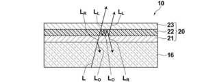
ここで、導光部材10の光透過制御層20の作用について、図2を用いて詳細に説明する。図2は導光部材10の概略構成を示す断面模式図である。
ここでは、反射偏光子層21は、右円偏光は透過し他の偏光は反射する反射偏光子層とし、反射偏光子層23は、左円偏光は透過し他の偏光は反射する反射偏光子層とし、偏光変換層22における偏光変換部材は、λ/8のリタデーションを有する複屈折体とする。
ここでは、反射偏光子層21は、右円偏光は透過し他の偏光は反射する反射偏光子層とし、反射偏光子層23は、左円偏光は透過し他の偏光は反射する反射偏光子層とし、偏光変換層22における偏光変換部材は、λ/8のリタデーションを有する複屈折体とする。
光源14から出射された光Lは様々な偏光方向の光を持つが、導光板16内を伝搬して進行方向が主面と直交する方向に近づけられた光Lのうち、右円偏光LRは光反射偏光子層21を透過する。このとき、光反射偏光子層21を透過する光は、完全な右円偏光LRだけでなく、右円偏光LRと偏光状態が近い光も若干透過する。(以後、完全な右円偏光LRおよび右円偏光LRと偏光状態が近い光を合わせて、右円偏光LRを中心とする光と呼称する。)
右円偏光LRを中心とする光以外の光LOは反射偏光子層21で反射し、導光板16に戻され、導光板16内で反射を繰り返すうちに偏光状態が導光部材10の光学特性に応じて僅かずつ変化し、反射偏光子層21を透過可能な偏光性が得られるまで導光板16内のみで光の再帰が繰り返されるため、光漏れ等による光のエネルギーロスは小さく、バックライトの高効率化にも寄与することができる。
右円偏光LRを中心とする光以外の光LOは反射偏光子層21で反射し、導光板16に戻され、導光板16内で反射を繰り返すうちに偏光状態が導光部材10の光学特性に応じて僅かずつ変化し、反射偏光子層21を透過可能な偏光性が得られるまで導光板16内のみで光の再帰が繰り返されるため、光漏れ等による光のエネルギーロスは小さく、バックライトの高効率化にも寄与することができる。
光反射偏光子層21を透過した右円偏光LRを中心とする光はλ/8のリタデーションを有する偏光変換層22において左円偏光LLに近づく偏光状態に変換され、右円偏光LRを中心とする光のうち反射偏光子層23を透過可能なほど左円偏光LLに近づいた光は、反射偏光子層23を透過して、液晶表示素子40のバックライト入射面に入射する。
反射偏光子層23を透過した光以外の光LOは反射偏光子層23で反射し、偏光変換層22に戻され、偏光変換層22内で反射を繰り返すうちに偏光状態が僅かずつ変化し、反射偏光子層21もしくは23を透過可能な偏光性が得られるまで偏光変換層22内のみで光の再帰が繰り返されるため、光漏れ等による光のエネルギーロスは小さく、バックライト光利用の高効率化にも寄与することができる。
反射偏光子層23を透過した光以外の光LOは反射偏光子層23で反射し、偏光変換層22に戻され、偏光変換層22内で反射を繰り返すうちに偏光状態が僅かずつ変化し、反射偏光子層21もしくは23を透過可能な偏光性が得られるまで偏光変換層22内のみで光の再帰が繰り返されるため、光漏れ等による光のエネルギーロスは小さく、バックライト光利用の高効率化にも寄与することができる。
上記の構成とした場合、反射偏光子層21を透過した光のうち、一度で偏光変換層22および反射偏光子層23まで透過できる光は、全体の約15%程度であり、残りの光は上記の通り導光部材10内で反射を繰り返して、いずれ反射偏光子層23から出射される。
すなわち、導光部材10を曲げて導光部材10内の全反射条件が崩れ、意図しない部分から光が漏れるようになった場合でも、ほとんどの光が光透過制御層20を直接透過することなく、導光部材10内に戻されて反射を繰り返すようになるので、最終的にバックライトの輝度の均一化が図られ、これによりバックライトの正面輝度の低下を抑えることが可能になる。
すなわち、導光部材10を曲げて導光部材10内の全反射条件が崩れ、意図しない部分から光が漏れるようになった場合でも、ほとんどの光が光透過制御層20を直接透過することなく、導光部材10内に戻されて反射を繰り返すようになるので、最終的にバックライトの輝度の均一化が図られ、これによりバックライトの正面輝度の低下を抑えることが可能になる。
なお、上記の構成において、偏光変換層22における偏光変換部材をλ/4のリタデーションを有する複屈折体とした場合には、反射偏光子層21を透過した光のうち、一度で偏光変換層22および反射偏光子層23まで透過できる光は、全体の約50%程度となる。また、上記の構成において、偏光変換層22における偏光変換部材をλ/2のリタデーションを有する複屈折体とした場合には、反射偏光子層21を透過した光のうち、一度で偏光変換層22および反射偏光子層23まで透過できる光は、全体の約100%程度となる。このように、偏光変換層22とこれを挟む反射偏光子層21、23との構成の関係によって、光の直接透過量を調節することができる。
また、導光部材10が出射する光が既に偏光性を有するため、液晶表示素子40とバックライトユニットとの間に通常設けられる、液晶表示素子40に入射する光を所定の偏光にするための偏光反射型輝度向上フィルムおよび/または偏光板を省略することができるため、薄型化・軽量化およびコスト低減に寄与することができる。また、所望の偏光性が得られるまで導光部材10内のみで光の再帰が繰り返されるため、光漏れ等による光のエネルギーロスは小さく、バックライトの高効率化にも寄与することができる。
なお、上記とは逆に、反射偏光子層21は、左円偏光は透過し他の偏光は反射する反射偏光子層とし、反射偏光子層23は、右円偏光は透過し他の偏光は反射する反射偏光子層とした場合や、反射偏光方向が異なる2つの反射偏光子層21、23について、一方が所定の直線偏光は透過し他の偏光は反射する反射偏光子層、他方が一方の反射偏光子層とは90°角度が傾いた直線偏光は透過し他の偏光は反射する反射偏光子層の組み合わせとした場合、さらには、上記以外の態様とした場合においても、光透過制御の原理は同様である。
なお、偏光変換層22における偏光変換部材としては、上記のような複屈折体または偏光解消体に限らず、図3に示すように、2つの透明電極層22a、22eの間に液晶物質が充填された液晶層22cを有する液晶セルとしてもよい。この液晶セルは、具体的には反射偏光子層21側から順に、透明電極層22a、配向膜22b、液晶層22c、配向膜22d、および、透明電極層22eが積層されてなるものである。この液晶セルは、2つの透明電極層22a、22e間に印加する電圧を調整することで、液晶層22cのリタデーションを任意に調節することができる。
また、透明電極層22a、22eは、各々、偏光変換層22の主面全体を覆う単一の面状電極に限らず、例えば複数の線状電極を並設する等、複数の電極から構成してもよい。透明電極層22aおよび/または22eを複数の電極から構成することで、液晶層22cの主面におけるリタデーション分布を任意に調節することができる。
偏光変換層22をこのような液晶セルとすることで、輝度の面内均一性を電圧で調整することができ、また、時間的に輝度を調整したり、面内で部分的に輝度を調整することもできるため、エリアバックライト(ローカルディミング型バックライト)として用いるにも好適である。
この液晶セルの構成の具体例については、後述の実施例において例示する。
また、透明電極層22a、22eは、各々、偏光変換層22の主面全体を覆う単一の面状電極に限らず、例えば複数の線状電極を並設する等、複数の電極から構成してもよい。透明電極層22aおよび/または22eを複数の電極から構成することで、液晶層22cの主面におけるリタデーション分布を任意に調節することができる。
偏光変換層22をこのような液晶セルとすることで、輝度の面内均一性を電圧で調整することができ、また、時間的に輝度を調整したり、面内で部分的に輝度を調整することもできるため、エリアバックライト(ローカルディミング型バックライト)として用いるにも好適である。
この液晶セルの構成の具体例については、後述の実施例において例示する。
光源14としては、LED(Light Emitting Diode)等の点光源であってもよいし、棒状の蛍光等等のライン光源であってもよく、従来のエッジライト型バックライトユニットで用いられている公知の光源を、各種、利用することができる。
なお、本実施形態では導光板16の端面16aから光を入射するエッジライト型バックライトユニットとしているが、本発明はエッジライト型バックライトユニットに限定されるものではなく、導光板16の第2の主面16cから光を入射する直下型バックライトユニットとすることもできる。
また、バックライトユニットはエリアごとに光源の明るさを変えられるローカルディミング型のバックライトでもよく、公知の光源を各種利用することができる。ローカルディミング型バックライトについては、例えば、特開2010-049125号公報や、特開2011-198468号公報等に記載がある。
なお、本実施形態では導光板16の端面16aから光を入射するエッジライト型バックライトユニットとしているが、本発明はエッジライト型バックライトユニットに限定されるものではなく、導光板16の第2の主面16cから光を入射する直下型バックライトユニットとすることもできる。
また、バックライトユニットはエリアごとに光源の明るさを変えられるローカルディミング型のバックライトでもよく、公知の光源を各種利用することができる。ローカルディミング型バックライトについては、例えば、特開2010-049125号公報や、特開2011-198468号公報等に記載がある。
裏面側反射板12は、導光板16の第2の主面16cから出射した光を導光板16に向かって反射するものである。このような裏面側反射板12を有することにより、光の利用効率を向上できる。裏面側反射板12は、特に制限なく、公知のものが、各種、利用可能である。光を効率的に用いるために、吸収が小さく反射率が高い反射面を有することが好ましい。例えば、白色PETやポリエステル系樹脂を用いた多層膜フィルムからなる反射面を有するものが好適であるが、これに限るものではない。ポリエステル系樹脂を用いた多層膜フィルムとしては、例えば、3M社製のESR(商品名)が挙げられる。
なお、裏面側反射板12は、図1に示したように、導光板16の第2の主面16cと離間して配置されていてもよいし、導光板16の第2の主面16cに粘着剤等により接着されていてもよい。裏面側反射板12が導光板16と接着されているとき、導光板16を伝搬する光は、導光板16の第1の主面16bと裏面側反射板12の反射面12aとの間で反射を繰り返し導波される。また、裏面側反射板12と反射偏光子層23の間に量子ドットに代表される波長変換層または波長変換パターン層を配置してもよい。導光板内を繰り返し再帰される光によって効率的に波長変換することができる。
以上、本発明の液晶表示装置について詳細に説明したが、本発明は上述の例に限定はされず、本発明の要旨を逸脱しない範囲において、各種の改良や変更を行ってもよいのは、もちろんである。
以下に実施例を挙げて本発明の特徴をさらに具体的に説明する。なお、以下に示す材料、使用量、割合、処理内容、処理手順等は、本発明の趣旨を逸脱しない限り、適宜、変更することができる。また、本発明の趣旨を逸脱しない限り、以下に示す構成以外の構成とすることもできる。すなわち、本発明の構成は以下に示す具体例に限定されるものではない。なお、特に断りのない限り、「部」、「%」は質量基準である。また、各リタデーションはAxoScan OPMF-1(オプトサイエンス社製)を用い、波長560nmで測定した値である。
[比較例1]
折り曲げていない平坦な導光部材として、厚さ400μmでA6サイズとしたアクリル導光板のみからなる導光部材を作製した。
また、比較対象となる折り曲げた導光部材として、図4に示すように、上記と同じA4サイズのアクリル導光板の中心付近に半径20mmの鉄棒50を約160度に加熱したものを押しつけてゆっくりと曲げることによって、90°折り曲げた導光部材を作製した。
折り曲げていない平坦な導光部材として、厚さ400μmでA6サイズとしたアクリル導光板のみからなる導光部材を作製した。
また、比較対象となる折り曲げた導光部材として、図4に示すように、上記と同じA4サイズのアクリル導光板の中心付近に半径20mmの鉄棒50を約160度に加熱したものを押しつけてゆっくりと曲げることによって、90°折り曲げた導光部材を作製した。
[実施例1a]
まず導光部材1a-1の作製を行った。
比較例1の平坦なアクリル導光部材に、下記構成の光透過制御層を積層した。
<<第1の反射偏光子層の貼合>>
直線偏光反射フィルムとしては、アップル社製のiPad Air(登録商標)を分解し、輝度向上フィルムとして用いられているフィルムを抜き出して用いた。
このフィルムを比較例1の平坦なアクリル導光部材の片面に総研化学社製SK2057で貼合した。
まず導光部材1a-1の作製を行った。
比較例1の平坦なアクリル導光部材に、下記構成の光透過制御層を積層した。
<<第1の反射偏光子層の貼合>>
直線偏光反射フィルムとしては、アップル社製のiPad Air(登録商標)を分解し、輝度向上フィルムとして用いられているフィルムを抜き出して用いた。
このフィルムを比較例1の平坦なアクリル導光部材の片面に総研化学社製SK2057で貼合した。
<<偏光変換層の作製>>
以下の様に、λ/16層である偏光変換層1を作製した。
以下の様に、λ/16層である偏光変換層1を作製した。
<剥離層用塗布液FL-1の調製>
下記の組成物を調製し、孔径0.45μmのポリプロピレン製フィルタでろ過して、剥離層用塗布液FL-1として用いた。
下記の組成物を調製し、孔径0.45μmのポリプロピレン製フィルタでろ過して、剥離層用塗布液FL-1として用いた。
・剥離層用塗布液組成(質量部)
ポリメチルメタクリレート(質量平均分子量50,000) 16.00
メチルエチルケトン 74.00
シクロヘキサノン 10.00
ポリメチルメタクリレート(質量平均分子量50,000) 16.00
メチルエチルケトン 74.00
シクロヘキサノン 10.00
<配向層用塗布液AL-1の調製>
下記の組成物を調製し、孔径30μmのポリプロピレン製フィルタでろ過して、配向層用塗布液AL-1として用いた。
下記の組成物を調製し、孔径30μmのポリプロピレン製フィルタでろ過して、配向層用塗布液AL-1として用いた。
・配向層用塗布液組成(質量部)
ポリビニルアルコール(PVA205、クラレ(株)製) 3.23
ポリビニルピロリドン(Luvitec K30、BASF社製)1.50
蒸留水 57.11
メタノール 38.16
ポリビニルアルコール(PVA205、クラレ(株)製) 3.23
ポリビニルピロリドン(Luvitec K30、BASF社製)1.50
蒸留水 57.11
メタノール 38.16
<光学異方性層用塗布液LC-1の調製>
下記の組成物を調製後、孔径0.45μmのポリプロピレン製フィルタでろ過して、光学異方性層用塗布液LC-1として用いた。
LC-1-1は2つの反応性基を有する液晶化合物であり、2つの反応性基の片方はラジカル性の反応性基であるアクリル基、他方はカチオン性の反応性基であるオキセタン基である。
下記の組成物を調製後、孔径0.45μmのポリプロピレン製フィルタでろ過して、光学異方性層用塗布液LC-1として用いた。
LC-1-1は2つの反応性基を有する液晶化合物であり、2つの反応性基の片方はラジカル性の反応性基であるアクリル基、他方はカチオン性の反応性基であるオキセタン基である。
・光学異方性層用塗布液組成(質量部)
重合性液晶化合物(LC-1-1) 32.88
水平配向剤(LC-1-2) 0.05
カチオン系光重合開始剤
(CPI100-P、サンアプロ株式会社製) 0.66
重合制御剤
(IRGANOX1076、チバ・スペシャルティ・ケミカルズ(株)製)
0.07
メチルエチルケトン 46.34
シクロヘキサノン 20.00
重合性液晶化合物(LC-1-1) 32.88
水平配向剤(LC-1-2) 0.05
カチオン系光重合開始剤
(CPI100-P、サンアプロ株式会社製) 0.66
重合制御剤
(IRGANOX1076、チバ・スペシャルティ・ケミカルズ(株)製)
0.07
メチルエチルケトン 46.34
シクロヘキサノン 20.00

(LC-1-1)

(LC-1-2)
なお、上記化学式2において、数値はモルである。
<添加剤層用塗布液OC-1の調製>
下記の組成物を調製後、孔径0.45μmのポリプロピレン製フィルタでろ過して、転写接着層用塗布液OC-1として用いた。ラジカル光重合開始剤RPI-1としては2-トリクロロメチル-5-(p-スチリルスチリル)1,3,4-オキサジアゾールを用いた。B-1はメタクリル酸メチルとメタクリル酸の共重合体で共重合組成比(モル比)=60/40である。
下記の組成物を調製後、孔径0.45μmのポリプロピレン製フィルタでろ過して、転写接着層用塗布液OC-1として用いた。ラジカル光重合開始剤RPI-1としては2-トリクロロメチル-5-(p-スチリルスチリル)1,3,4-オキサジアゾールを用いた。B-1はメタクリル酸メチルとメタクリル酸の共重合体で共重合組成比(モル比)=60/40である。
・添加剤層用塗布液組成(質量部)
バインダ(B-1) 7.63
ラジカル光重合開始剤(RPI-1) 0.49
界面活性剤溶液 0.03
(メガファックF-176PF、大日本インキ化学工業(株)製)
メチルエチルケトン 68.89
酢酸エチル 15.34
酢酸ブチル 7.63
バインダ(B-1) 7.63
ラジカル光重合開始剤(RPI-1) 0.49
界面活性剤溶液 0.03
(メガファックF-176PF、大日本インキ化学工業(株)製)
メチルエチルケトン 68.89
酢酸エチル 15.34
酢酸ブチル 7.63

(B-1)
<感熱性接着層用塗布液AD-2の調製>
下記の組成物を調製後、孔径0.45μmのポリプロピレン製フィルタでろ過して、接着層用塗布液AD-2として用いた。
下記の組成物を調製後、孔径0.45μmのポリプロピレン製フィルタでろ過して、接着層用塗布液AD-2として用いた。
・感熱性接着層用塗布液組成(質量部)
ポリエステル系ホットメルト樹脂溶液 37.50
(PES375S40、東亞合成(株)製)
メチルエチルケトン 62.50
ポリエステル系ホットメルト樹脂溶液 37.50
(PES375S40、東亞合成(株)製)
メチルエチルケトン 62.50
<複屈折材P-1の作製>
厚さ50μmのポリエチレンナフタレートフィルム(テオネックスQ83、帝人デュポン(株)製)の上にアルミニウムを60nm蒸着し、反射層つき支持体を作製した。そのアルミニウムを蒸着した面上にワイヤーバーを用いて剥離層用塗布液FL-1を塗布、乾燥して剥離層とした。剥離層の乾燥膜厚は2.0μmであった。乾燥した剥離層上にワイヤーバーを用いて配向層用塗布液AL-1を塗布、乾燥して配向層とした。配向層の乾燥膜厚は0.5μmであった。
厚さ50μmのポリエチレンナフタレートフィルム(テオネックスQ83、帝人デュポン(株)製)の上にアルミニウムを60nm蒸着し、反射層つき支持体を作製した。そのアルミニウムを蒸着した面上にワイヤーバーを用いて剥離層用塗布液FL-1を塗布、乾燥して剥離層とした。剥離層の乾燥膜厚は2.0μmであった。乾燥した剥離層上にワイヤーバーを用いて配向層用塗布液AL-1を塗布、乾燥して配向層とした。配向層の乾燥膜厚は0.5μmであった。
次いで配向層をラビング処理した後、ワイヤーバーを用いて光学異方性層用塗布液LC-1を塗布、膜面温度90℃で2分間乾燥して液晶相状態とした後、空気下にて160W/cmの空冷メタルハライドランプ(アイグラフィックス(株)製)を用いて紫外線を照射してその配向状態を固定化して厚さ0.2μmの光学異方性層を形成した。この際用いた紫外線の照度はUV-A領域(波長320nm~400nmの積算)において600mW/cm2、照射量はUV-A領域において300mJ/cm2であった。最後に、光学異方性層の上にワイヤーバーを用いて添加剤層用塗布液OC-1を塗布、乾燥して膜厚0.8μmの添加剤層を形成し、複屈折材P-1を作製した。
<偏光変換層1の作製>
複屈折材P-1をレーザ走査露光によるデジタル露光機(INPREX IP-3600H、富士フイルム(株)製)にて、40mJ/cm2の露光量を用いて全面露光した。その後遠赤外線ヒータ連続炉を用い、膜面温度が210℃となるように15分間加熱して、光学異方性層を作製した。
最後に、添加剤層上にワイヤーバーを用いて感熱性接着層用塗布液AD-2を塗布、乾燥して膜厚2.0μmの感熱性接着層を形成し、複屈折パターン転写箔F-1を作製し、偏光変換層とした。この偏光変換層1のリタデーションをガラス基板に転写し測定したところ、35nmであった。
複屈折材P-1をレーザ走査露光によるデジタル露光機(INPREX IP-3600H、富士フイルム(株)製)にて、40mJ/cm2の露光量を用いて全面露光した。その後遠赤外線ヒータ連続炉を用い、膜面温度が210℃となるように15分間加熱して、光学異方性層を作製した。
最後に、添加剤層上にワイヤーバーを用いて感熱性接着層用塗布液AD-2を塗布、乾燥して膜厚2.0μmの感熱性接着層を形成し、複屈折パターン転写箔F-1を作製し、偏光変換層とした。この偏光変換層1のリタデーションをガラス基板に転写し測定したところ、35nmであった。
このλ/16層である偏光変換層1をラミネーターを用いてローラー温度150℃、面圧0.2Mpa、搬送速度1.0m/分で、前述の第1の反射偏光子層の上に熱圧転写した。
<<第2の反射偏光子層の貼合>>
偏光変換層の上に、さらに第2の反射偏光子層として第1の反射偏光子層と同じ直線偏光反射フィルムを、第1の反射偏光子層と偏光方向が直交するように総研化学社製SK2057で貼合することで、図1に示す断面形状のような、アクリル導光板上に第1の反射偏光子層、偏光変換層、第2の反射偏光子層がこの順に積層されてなる光透過制御層が形成された、平坦な導光部材1a-1を得た。
偏光変換層の上に、さらに第2の反射偏光子層として第1の反射偏光子層と同じ直線偏光反射フィルムを、第1の反射偏光子層と偏光方向が直交するように総研化学社製SK2057で貼合することで、図1に示す断面形状のような、アクリル導光板上に第1の反射偏光子層、偏光変換層、第2の反射偏光子層がこの順に積層されてなる光透過制御層が形成された、平坦な導光部材1a-1を得た。
次に、導光部材1a-2の作製を行った。
導光部材1a-1と異なり平坦なアクリル導光部材を用いず、それ以外は導光部材1a-1と同様にして、第1の反射偏光子層、偏光変換層、第2の反射偏光子層がこの順に積層されてなる光透過制御層を作製した。
次に、比較例1の90°折り曲げたアクリル導光部材と、光透過制御層の第1の反射偏光子層を研化学社製SK2057を用いて貼合した。
これにより90°折り曲げ部分のある導光部材1a-2を作製した。
導光部材1a-1と異なり平坦なアクリル導光部材を用いず、それ以外は導光部材1a-1と同様にして、第1の反射偏光子層、偏光変換層、第2の反射偏光子層がこの順に積層されてなる光透過制御層を作製した。
次に、比較例1の90°折り曲げたアクリル導光部材と、光透過制御層の第1の反射偏光子層を研化学社製SK2057を用いて貼合した。
これにより90°折り曲げ部分のある導光部材1a-2を作製した。
[実施例1b]
実施例1a-1および1a-2の各々について、偏光変換層1をλ/8層である偏光変換層2としたものである。
複屈折材P-1の作製において、光学異方性層の厚さを0.4μmとした以外は、実施例1a-1および1a-2の作製方法と同じである。この偏光変換層2のリタデーションをガラス基板に転写し測定したところ、70nmであった。
実施例1a-1および1a-2の各々について、偏光変換層1をλ/8層である偏光変換層2としたものである。
複屈折材P-1の作製において、光学異方性層の厚さを0.4μmとした以外は、実施例1a-1および1a-2の作製方法と同じである。この偏光変換層2のリタデーションをガラス基板に転写し測定したところ、70nmであった。
[実施例1c]
実施例1a-1および1a-2の各々について、偏光変換層1をλ/4層である偏光変換層3としたものである。
複屈折材P-1の作製において、光学異方性層の厚さを0.8μmとした以外は、実施例1a-1および1a-2の作製方法と同じである。この偏光変換層3のリタデーションをガラス基板に転写し測定したところ、135nmであった。
実施例1a-1および1a-2の各々について、偏光変換層1をλ/4層である偏光変換層3としたものである。
複屈折材P-1の作製において、光学異方性層の厚さを0.8μmとした以外は、実施例1a-1および1a-2の作製方法と同じである。この偏光変換層3のリタデーションをガラス基板に転写し測定したところ、135nmであった。
[実施例1d]
実施例1a-1および1a-2の各々について、偏光変換層1をλ/2層である偏光変換層4としたものである。
複屈折材P-1の作製において、光学異方性層の厚さを1.6μmとした以外は、実施例1a-1および1a-2の作製方法と同じである。この偏光変換層4のリタデーションをガラス基板に転写し測定したところ、270nmであった。
実施例1a-1および1a-2の各々について、偏光変換層1をλ/2層である偏光変換層4としたものである。
複屈折材P-1の作製において、光学異方性層の厚さを1.6μmとした以外は、実施例1a-1および1a-2の作製方法と同じである。この偏光変換層4のリタデーションをガラス基板に転写し測定したところ、270nmであった。
[実施例2]
まず導光部材2-1の作製を行った。
比較例1の平坦なアクリル導光部材に、下記構成の光透過制御層を積層した。
<<第1の反射偏光子層の作製>>
下記に示す組成物を、25℃に保温された容器中にて、攪拌、溶解させ、コレステリック液晶インク液(液晶組成物)を調製した。コレステリック液晶インク液(液晶組成物)には、下記構造の右捩れ用キラル剤Aまたは下記構造の左捩れ用キラル剤Bが含まれるが、それ以外に、下記「コレステリック液晶インク液(質量部)」に示すものが含有される。コレステリック液晶インク液(液晶組成物)では、下記に示す他に含有されるものの量(質量部)を変えることなく、右捩れ用キラル剤Aまたは左捩れ用キラル剤Bのキラル剤の種類と右捩れ用キラル剤Aと左捩れ用キラル剤Bの量(質量部)のみを、選択中心波長に応じて下記表1に示すように調整することにより、特定の選択中心波長を反射するためのコレステリック液晶を調製することができる。右円偏光を反射するドットを形成する場合、キラル剤としては、右捩れ用キラル剤Aだけを下記表1に示す選択中心波長に応じた量(質量部)添加する。左円偏光を反射するドットを形成する場合、キラル剤としては、左捩れ用キラル剤Bだけを下記表1に示す選択中心波長に応じた量(質量部)添加する。
まず導光部材2-1の作製を行った。
比較例1の平坦なアクリル導光部材に、下記構成の光透過制御層を積層した。
<<第1の反射偏光子層の作製>>
下記に示す組成物を、25℃に保温された容器中にて、攪拌、溶解させ、コレステリック液晶インク液(液晶組成物)を調製した。コレステリック液晶インク液(液晶組成物)には、下記構造の右捩れ用キラル剤Aまたは下記構造の左捩れ用キラル剤Bが含まれるが、それ以外に、下記「コレステリック液晶インク液(質量部)」に示すものが含有される。コレステリック液晶インク液(液晶組成物)では、下記に示す他に含有されるものの量(質量部)を変えることなく、右捩れ用キラル剤Aまたは左捩れ用キラル剤Bのキラル剤の種類と右捩れ用キラル剤Aと左捩れ用キラル剤Bの量(質量部)のみを、選択中心波長に応じて下記表1に示すように調整することにより、特定の選択中心波長を反射するためのコレステリック液晶を調製することができる。右円偏光を反射するドットを形成する場合、キラル剤としては、右捩れ用キラル剤Aだけを下記表1に示す選択中心波長に応じた量(質量部)添加する。左円偏光を反射するドットを形成する場合、キラル剤としては、左捩れ用キラル剤Bだけを下記表1に示す選択中心波長に応じた量(質量部)添加する。
<右捩れコレステリック液晶インク液(質量部)>
メトキシエチルアクリレート 145.0
下記の棒状液晶化合物の混合物 100.0
IRGACURE(登録商標) 819 (BASF社製) 10.0
下記構造の右捩れ用キラル剤A 下記表1参照
下記構造の界面活性剤 0.08
メトキシエチルアクリレート 145.0
下記の棒状液晶化合物の混合物 100.0
IRGACURE(登録商標) 819 (BASF社製) 10.0
下記構造の右捩れ用キラル剤A 下記表1参照
下記構造の界面活性剤 0.08
<左捩れコレステリック液晶インク液(質量部)>
メトキシエチルアクリレート 145.0
下記の棒状液晶化合物の混合物 100.0
IRGACURE(登録商標) 819 (BASF社製) 10.0
下記構造の左捩れ用キラル剤B 下記表1参照
下記構造の界面活性剤 0.08
メトキシエチルアクリレート 145.0
下記の棒状液晶化合物の混合物 100.0
IRGACURE(登録商標) 819 (BASF社製) 10.0
下記構造の左捩れ用キラル剤B 下記表1参照
下記構造の界面活性剤 0.08




下記表1に基づき、選択中心波長、および反射する偏光の形態に応じて、コレステリック液晶インク液を調整した。

比較例1の平坦なアクリル導光部材の片面に、ポリビニルアルコール10質量部、水371質量部からなる配向膜塗布液を塗布、乾燥し、厚さ1μmの配向膜を形成した。次いで、このフィルムの長手方向に対し平行方向に連続的に配向膜上にラビング処理を実施した。
配向膜の上に、表1の中心選択波長450nmで右捩じれの液晶インクをバーコーターを用いて塗布し、10秒間室温にて乾燥後、100℃のオーブン中で2分間加熱(配向熟成)し、さらに30秒間紫外線を照射して、厚さ5μmのコレステリック液晶層を作製した。
さらに、その上に表1の中心選択波長550nmで右捩じれの液晶インクをバーコーターを用いて塗布し、10秒間室温にて乾燥後、100℃のオーブン中で2分間加熱(配向熟成)し、さらに30秒間紫外線を照射して、厚さ5μmのコレステリック液晶を下層の上に積層作製した。
さらに、その上に表1の中心選択波長650nmで右捩じれの液晶インクをバーコーターを用いて塗布し、10秒間室温にて乾燥後、100℃のオーブン中で2分間加熱(配向熟成)し、さらに30秒間紫外線を照射して、厚さ5μmのコレステリック液晶を下層の上に積層作製した。
さらに、その上に表1の中心選択波長750nmで右捩じれの液晶インクをバーコーターを用いて塗布し、10秒間室温にて乾燥後、100℃のオーブン中で2分間加熱(配向熟成)し、さらに30秒間紫外線を照射して、厚さ5μmのコレステリック液晶を下層の上に積層作製した。
このようにして、4層のコレステリック液晶の積層である、第1の反射偏光子層を作製した。この断面を走査型電子顕微鏡で観察したところ、層法線方向に螺旋軸を有し、コレステリックピッチが4層異なる層が積層した構造を有しており、そのピッチは中心選択波
長の450、550,650、750nmに対応していた。またAxoscanで反射スペクトルを測定したところ、右円偏光が450、550,650、750nmを中心とした4つの反射帯域で反射していることが確認でき、可視光領域から近赤外領域に向かって広い右円偏光の反射帯域を有していることが確認できた。
配向膜の上に、表1の中心選択波長450nmで右捩じれの液晶インクをバーコーターを用いて塗布し、10秒間室温にて乾燥後、100℃のオーブン中で2分間加熱(配向熟成)し、さらに30秒間紫外線を照射して、厚さ5μmのコレステリック液晶層を作製した。
さらに、その上に表1の中心選択波長550nmで右捩じれの液晶インクをバーコーターを用いて塗布し、10秒間室温にて乾燥後、100℃のオーブン中で2分間加熱(配向熟成)し、さらに30秒間紫外線を照射して、厚さ5μmのコレステリック液晶を下層の上に積層作製した。
さらに、その上に表1の中心選択波長650nmで右捩じれの液晶インクをバーコーターを用いて塗布し、10秒間室温にて乾燥後、100℃のオーブン中で2分間加熱(配向熟成)し、さらに30秒間紫外線を照射して、厚さ5μmのコレステリック液晶を下層の上に積層作製した。
さらに、その上に表1の中心選択波長750nmで右捩じれの液晶インクをバーコーターを用いて塗布し、10秒間室温にて乾燥後、100℃のオーブン中で2分間加熱(配向熟成)し、さらに30秒間紫外線を照射して、厚さ5μmのコレステリック液晶を下層の上に積層作製した。
このようにして、4層のコレステリック液晶の積層である、第1の反射偏光子層を作製した。この断面を走査型電子顕微鏡で観察したところ、層法線方向に螺旋軸を有し、コレステリックピッチが4層異なる層が積層した構造を有しており、そのピッチは中心選択波
長の450、550,650、750nmに対応していた。またAxoscanで反射スペクトルを測定したところ、右円偏光が450、550,650、750nmを中心とした4つの反射帯域で反射していることが確認でき、可視光領域から近赤外領域に向かって広い右円偏光の反射帯域を有していることが確認できた。
<<偏光変換層の作製>>
実施例1bと同様である。
実施例1bと同様である。
<<第2の反射偏光子層の作製>>
仮支持体として富士フイルム製PET(厚さ75μm)を準備し、連続的にラビング処理を施した。上記仮支持体上に第2の反射偏光子層を以下の様に作製した。
第2の反射偏光子層は第1の反射偏光子層の支持体を仮支持体に変更した点、および右捩れ用キラル剤Aを左捩れ用キラル剤Bに変更したコレステリック液晶インク液を用いた点(表1を参照)以外は、第1の反射偏光子層と作製法は同じである。このようにして、第2の反射偏光子層を作製した。
第1の反射偏光子層と同様に、断面を走査型電子顕微鏡で観察したところ、層法線方向に螺旋軸を有し、コレステリックピッチが4層異なる層が積層した構造を有しており、そのピッチは中心選択波長の450、550,650、750nmに対応していた。またAxoscanで反射スペクトルを測定したところ、左円偏光が450、550,650、750nmを中心とした4つの反射帯域で反射していることが確認でき、可視光領域から近赤外領域に向かって広い左円偏光の反射帯域を有していることが確認できた。
仮支持体として富士フイルム製PET(厚さ75μm)を準備し、連続的にラビング処理を施した。上記仮支持体上に第2の反射偏光子層を以下の様に作製した。
第2の反射偏光子層は第1の反射偏光子層の支持体を仮支持体に変更した点、および右捩れ用キラル剤Aを左捩れ用キラル剤Bに変更したコレステリック液晶インク液を用いた点(表1を参照)以外は、第1の反射偏光子層と作製法は同じである。このようにして、第2の反射偏光子層を作製した。
第1の反射偏光子層と同様に、断面を走査型電子顕微鏡で観察したところ、層法線方向に螺旋軸を有し、コレステリックピッチが4層異なる層が積層した構造を有しており、そのピッチは中心選択波長の450、550,650、750nmに対応していた。またAxoscanで反射スペクトルを測定したところ、左円偏光が450、550,650、750nmを中心とした4つの反射帯域で反射していることが確認でき、可視光領域から近赤外領域に向かって広い左円偏光の反射帯域を有していることが確認できた。
第2の反射偏光子層の塗布面と、λ/8層である偏光変換層2を、総研化学社製SK2057を使用して貼合し、貼合後に第2の反射偏光子層側の仮支持体を剥離することで、図1に示す断面形状のような、アクリル導光板上に第1の反射偏光子層、偏光変換層、第2の反射偏光子層がこの順に積層されてなる光透過制御層が形成された、平坦な導光部材2-1を得た。
次に、導光部材2-2の作製を行った。まず、第1の反射偏光子層の作製において、平坦なアクリル導光部材を用いる代わりに、仮支持体である富士フイルム製PET(厚さ75μm)を用い、第1の反射偏光子層を、偏光変換層上に転写する以外は導光部材1-1と同様にして、仮支持体上に第2の反射偏光子層、偏光変換層、第1の反射偏光子層がこの順に積層された転写部材を作製した。
次に、90°折り曲げたアクリル導光部材に、第1の反射偏光子層、偏光変換層、第2の反射偏光子層がこの順になるよう、仮支持体から転写した。この際、折り曲げたアクリル導光部材と第1の反射偏光子層を研化学社製SK2057を用いて貼合した。
これにより90°折り曲げ部分のある導光部材2-2を作製した。
次に、90°折り曲げたアクリル導光部材に、第1の反射偏光子層、偏光変換層、第2の反射偏光子層がこの順になるよう、仮支持体から転写した。この際、折り曲げたアクリル導光部材と第1の反射偏光子層を研化学社製SK2057を用いて貼合した。
これにより90°折り曲げ部分のある導光部材2-2を作製した。
[実施例3]
実施例1aの導光部材において、光透過制御層の偏光変換層を散乱材(偏光解消体)により構成するように変更したものである。
散乱材を構成する透光性樹脂として、ジペンタエリスリトールヘキサアクリレート{日本化薬(株)製}を100質量部、透光性粒子としてメラミン樹脂粒子「オプトビーズ2000M」を9質量部、及び重合開始剤「イルガキュア184」6質量部を混合してメチルエチルケトン/メチルイソブチルケトン(30/70質量比)により固形分50質量%になるように調製した。
乾燥膜厚1.0μmとなるように上記透光性樹脂を塗工、溶媒乾燥後、160W/cmの空冷メタルハライドランプ(アイグラフィックス製)を用いて、照度1.5kW/cm2、照射量95mJ/cm2の紫外線を照射して硬化させ、散乱材からなる偏光変換層を形成した。
実施例1aの導光部材において、光透過制御層の偏光変換層を散乱材(偏光解消体)により構成するように変更したものである。
散乱材を構成する透光性樹脂として、ジペンタエリスリトールヘキサアクリレート{日本化薬(株)製}を100質量部、透光性粒子としてメラミン樹脂粒子「オプトビーズ2000M」を9質量部、及び重合開始剤「イルガキュア184」6質量部を混合してメチルエチルケトン/メチルイソブチルケトン(30/70質量比)により固形分50質量%になるように調製した。
乾燥膜厚1.0μmとなるように上記透光性樹脂を塗工、溶媒乾燥後、160W/cmの空冷メタルハライドランプ(アイグラフィックス製)を用いて、照度1.5kW/cm2、照射量95mJ/cm2の紫外線を照射して硬化させ、散乱材からなる偏光変換層を形成した。
[実施例4]
実施例2の導光部材において、光透過制御層の偏光変換層を実施例3と同じ散乱材(偏光解消体)により構成するように変更したものである。
実施例2の導光部材において、光透過制御層の偏光変換層を実施例3と同じ散乱材(偏光解消体)により構成するように変更したものである。
[実施例5]
実施例1aの導光部材において、光透過制御層の偏光変換層を液晶セルにより構成するように変更したものである。
この液晶セルは、特開2000-347170号公報を参考に作製した。先ず、2枚のポリカーボネートフィルムの片面に透明電極ITO(Indium Tin Oxide)をスパッタ製膜した。次に、配向剤として低温硬化型ポリイミドである日立化成製 STX-24をN-メチルピロリドンに希釈溶解して、ポリカーボネートフィルムのITO上にスピンコートした。熱硬化後にラビングマシンにてポリエステル系のラビングロールでラビングした。1枚のポリカーボネートフィルムのITO側にフォトレックS(積水化学社製)を表示部外周に塗布、それに続いて液晶ディスペンサーにて、スぺーサーとして積水ファインケミカル製ミクロパールを分散したZLI-4792(メルク社製)を滴下後、もう1枚のポリカーボネートフィルムをラビング方向が反平行(アンチパラレル)になるように合わせ、真空滴下法にて液晶を注入してセルを作製した。セルギャップは3μmであった。
2つの基板のITOに矩形波60Hzの電圧を印加すると電圧が大きくなるにつれリタデーションは小さくなり、電圧0Vの時リタデーションは300nmで、電圧3Vで140nm、5Vで60nm、10Vで28nm、15Vで17nmであった。
実施例1aの導光部材において、光透過制御層の偏光変換層を液晶セルにより構成するように変更したものである。
この液晶セルは、特開2000-347170号公報を参考に作製した。先ず、2枚のポリカーボネートフィルムの片面に透明電極ITO(Indium Tin Oxide)をスパッタ製膜した。次に、配向剤として低温硬化型ポリイミドである日立化成製 STX-24をN-メチルピロリドンに希釈溶解して、ポリカーボネートフィルムのITO上にスピンコートした。熱硬化後にラビングマシンにてポリエステル系のラビングロールでラビングした。1枚のポリカーボネートフィルムのITO側にフォトレックS(積水化学社製)を表示部外周に塗布、それに続いて液晶ディスペンサーにて、スぺーサーとして積水ファインケミカル製ミクロパールを分散したZLI-4792(メルク社製)を滴下後、もう1枚のポリカーボネートフィルムをラビング方向が反平行(アンチパラレル)になるように合わせ、真空滴下法にて液晶を注入してセルを作製した。セルギャップは3μmであった。
2つの基板のITOに矩形波60Hzの電圧を印加すると電圧が大きくなるにつれリタデーションは小さくなり、電圧0Vの時リタデーションは300nmで、電圧3Vで140nm、5Vで60nm、10Vで28nm、15Vで17nmであった。
[評価方法]
比較例1および実施例1a~5毎に、平坦な導光部材の正面輝度と90°折り曲げ部分のある導光部材の正面輝度とを比較した。なお、正面輝度は、図4(90°折り曲げた導光部材の例)に示すように、導光部材10の端面から光を入射し、トプコン社のBM-5Aを用いて、導光部材の中央位置における面の法線N方向から輝度を測定したものである。
上記の評価結果を表2に示す。
比較例1および実施例1a~5毎に、平坦な導光部材の正面輝度と90°折り曲げ部分のある導光部材の正面輝度とを比較した。なお、正面輝度は、図4(90°折り曲げた導光部材の例)に示すように、導光部材10の端面から光を入射し、トプコン社のBM-5Aを用いて、導光部材の中央位置における面の法線N方向から輝度を測定したものである。
上記の評価結果を表2に示す。

<評価基準>
平坦な導光部材の正面輝度に対する、90°折り曲げ部分のある導光部材の正面輝度の割合(正面輝度維持率)について、下記の通りとする。
A:100%以下~85%以上
B:85%未満~75%以上
C:75%未満~65%以上
D:65%未満~60%以上
E:60%未満
この評価においては、導光部材が90°曲がった状態でも正面輝度が低下していないことが好ましく、すなわちAが最も良好である。
平坦な導光部材の正面輝度に対する、90°折り曲げ部分のある導光部材の正面輝度の割合(正面輝度維持率)について、下記の通りとする。
A:100%以下~85%以上
B:85%未満~75%以上
C:75%未満~65%以上
D:65%未満~60%以上
E:60%未満
この評価においては、導光部材が90°曲がった状態でも正面輝度が低下していないことが好ましく、すなわちAが最も良好である。
上記表2に示されるように、光透過制御層を持たない従来の導光板(比較例1)では、正面輝度維持率の評価がEであり、導光部材を90°曲げた状態で正面輝度が大きく低下してしまうのに対し、本発明の導光部材(実施例1a~5)では、正面輝度維持率の評価がC以上であり、従来の導光板と比較して正面輝度の低下が少ないことが分かる。
また、実施例1a~1dの評価結果により、2つの反射偏光子層の偏光方向が90°ずれているとき、偏光変換層はλ/8層(実施例1b)とした場合が、最も正面輝度維持率が高くなることが分かった。
また、実施例5については、電圧5Vのときにλ/8層と同等のリタデーションとなり、実施例1bと同じく正面輝度維持率の評価がAとなった。なお、表には示していないが、電圧3Vでは電圧5Vの時と比べ輝度が低くなりB評価となることが確認できた。また、電圧15Vでは電圧5Vの時と比べさらに輝度が小さくC評価となることが確認できた。これにより、電圧で輝度を調整できることが確認できた。
なお、平坦な状態で作製した導光部材を作製後に曲げた場合でも、上記のように曲げた状態で作製した導光部材と同様の効果が得られる。
以上より本発明の効果は明らかである。
以上より本発明の効果は明らかである。
1 液晶表示装置
10 導光部材
12 裏面側反射板
14 光源
16 導光板
16a 導光板の端面
16b 導光板の第1の主面
16c 導光板の第2の主面
20 光透過制御層
21 反射偏光子層
22 偏光変換層
23 反射偏光子層
40 液晶表示素子
50 鉄棒
L 光
LL 左円偏光
LO 他の偏光光
LR 右円偏光
N 法線方向
10 導光部材
12 裏面側反射板
14 光源
16 導光板
16a 導光板の端面
16b 導光板の第1の主面
16c 導光板の第2の主面
20 光透過制御層
21 反射偏光子層
22 偏光変換層
23 反射偏光子層
40 液晶表示素子
50 鉄棒
L 光
LL 左円偏光
LO 他の偏光光
LR 右円偏光
N 法線方向
Claims (9)
- 入射した光を導光して少なくとも一方の主面から出射させる導光層と、
前記導光層の前記光を出射する主面側において前記導光層に一体的に積層され、前記光の透過量を制御する光透過制御層とを有する導光部材であって、
前記光透過制御層は、2つの反射偏光子層の間において、偏光変換部材が全面に配設された偏光変換層を有するものである
ことを特徴とする導光部材。 - 前記偏光変換層の主面におけるリタデーション分布が均一である
請求項1記載の導光部材。 - 前記偏光変換層の主面におけるリタデーション分布が不均一である
請求項1記載の導光部材。 - 前記偏光変換部材は、2つの透明電極層の間に液晶物質が充填されてなる液晶セルである
請求項1から3のいずれか1項記載の導光部材。 - 前記偏光変換部材は、複屈折体である
請求項1から3のいずれか1項記載の導光部材。 - 前記偏光変換部材は、偏光解消体である
請求項1から3のいずれか1項記載の導光部材。 - 前記反射偏光子層は、複屈折高分子多層偏光フィルムである
請求項1から6のいずれか1項記載の導光部材。 - 前記反射偏光子層は、コレステリック液晶である
請求項1から6のいずれか1項記載の導光部材。 - 画像表示面と反対側のバックライト入射面からバックライトが入射される液晶表示素子と、
請求項1から8のいずれか1項記載の導光部材、および前記導光部材に光を入射する光源を有するバックライトユニットとを有し、
前記液晶表示素子の前記バックライト入射面と前記導光部材の前記光透過制御層とが対向し、かつ、前記液晶表示素子に設定された前記バックライトの入射時の偏光軸方向と前記導光部材から出射される光の偏光軸方向とが一致した状態で、前記液晶表示素子と前記導光部材とが一体的に積層されている
ことを特徴とする液晶表示装置。
Priority Applications (3)
| Application Number | Priority Date | Filing Date | Title |
|---|---|---|---|
| CN201780038659.8A CN109312900A (zh) | 2016-06-22 | 2017-06-21 | 导光部件及液晶显示装置 |
| JP2018524149A JP6945529B2 (ja) | 2016-06-22 | 2017-06-21 | 導光部材および液晶表示装置 |
| US16/221,578 US20190137818A1 (en) | 2016-06-22 | 2018-12-16 | Light guide member and liquid crystal display device |
Applications Claiming Priority (2)
| Application Number | Priority Date | Filing Date | Title |
|---|---|---|---|
| JP2016-123274 | 2016-06-22 | ||
| JP2016123274 | 2016-06-22 |
Related Child Applications (1)
| Application Number | Title | Priority Date | Filing Date |
|---|---|---|---|
| US16/221,578 Continuation US20190137818A1 (en) | 2016-06-22 | 2018-12-16 | Light guide member and liquid crystal display device |
Publications (1)
| Publication Number | Publication Date |
|---|---|
| WO2017221993A1 true WO2017221993A1 (ja) | 2017-12-28 |
Family
ID=60784613
Family Applications (1)
| Application Number | Title | Priority Date | Filing Date |
|---|---|---|---|
| PCT/JP2017/022914 Ceased WO2017221993A1 (ja) | 2016-06-22 | 2017-06-21 | 導光部材および液晶表示装置 |
Country Status (4)
| Country | Link |
|---|---|
| US (1) | US20190137818A1 (ja) |
| JP (1) | JP6945529B2 (ja) |
| CN (1) | CN109312900A (ja) |
| WO (1) | WO2017221993A1 (ja) |
Cited By (2)
| Publication number | Priority date | Publication date | Assignee | Title |
|---|---|---|---|---|
| JPWO2018079130A1 (ja) * | 2016-10-25 | 2019-07-25 | 富士フイルム株式会社 | 透過加飾フィルム |
| WO2020080355A1 (ja) * | 2018-10-17 | 2020-04-23 | 富士フイルム株式会社 | 投映像表示用部材、ウインドシールドガラスおよびヘッドアップディスプレイシステム |
Families Citing this family (10)
| Publication number | Priority date | Publication date | Assignee | Title |
|---|---|---|---|---|
| US10261321B2 (en) | 2005-11-08 | 2019-04-16 | Lumus Ltd. | Polarizing optical system |
| IL235642B (en) | 2014-11-11 | 2021-08-31 | Lumus Ltd | A compact head-up display system is protected by an element with a super-thin structure |
| JP7187022B2 (ja) * | 2016-10-09 | 2022-12-12 | ルムス エルティーディー. | 長方形導波路を使用する開口乗算器 |
| CN113031165B (zh) | 2016-11-08 | 2023-06-02 | 鲁姆斯有限公司 | 导光装置、其光学组件及其对应的生产方法 |
| JP6980209B2 (ja) | 2017-02-22 | 2021-12-15 | ルムス エルティーディー. | 光ガイド光学アセンブリ |
| JP7174929B2 (ja) | 2017-07-19 | 2022-11-18 | ルムス エルティーディー. | Loeを介するlcos照明 |
| WO2020174433A1 (en) | 2019-02-28 | 2020-09-03 | Lumus Ltd. | Compact collimated image projector |
| KR20210151782A (ko) | 2019-04-15 | 2021-12-14 | 루머스 리미티드 | 광-유도 광학 소자 제조 방법 |
| CA3155597C (en) | 2019-12-08 | 2023-02-14 | Lumus Ltd. | Optical systems with compact image projector |
| CN115176190B (zh) | 2020-05-24 | 2024-07-09 | 鲁姆斯有限公司 | 复合光导光学元件 |
Citations (6)
| Publication number | Priority date | Publication date | Assignee | Title |
|---|---|---|---|---|
| JP2000147429A (ja) * | 1998-11-10 | 2000-05-26 | Nitto Denko Corp | 偏光面光源装置及び液晶表示装置 |
| JP2004151559A (ja) * | 2002-10-31 | 2004-05-27 | Seiko Epson Corp | 表示装置及び電子機器 |
| JP2010221685A (ja) * | 2009-02-26 | 2010-10-07 | Dainippon Printing Co Ltd | 電磁波反射部材 |
| WO2011043208A1 (ja) * | 2009-10-05 | 2011-04-14 | 日本電気株式会社 | 光学素子、光源装置、及び投射型表示装置 |
| JP2013008446A (ja) * | 2011-06-22 | 2013-01-10 | Minebea Co Ltd | フレキシブル面状照明装置 |
| JP2016024289A (ja) * | 2014-07-18 | 2016-02-08 | 旭硝子株式会社 | 画像光投影用スクリーンおよび表示システム |
Family Cites Families (13)
| Publication number | Priority date | Publication date | Assignee | Title |
|---|---|---|---|---|
| JP4467840B2 (ja) * | 2000-07-31 | 2010-05-26 | 東芝モバイルディスプレイ株式会社 | 照明装置、及び導光板の製造方法 |
| WO2003091766A1 (fr) * | 2002-04-23 | 2003-11-06 | Nitto Denko Corporation | Polariseur, source de lumiere polarisante et unite d'affichage d'images utilisant ceux-ci |
| US8792070B2 (en) * | 2007-03-21 | 2014-07-29 | Honeywell International Inc. | Polarization plate for use in a liquid crystal display |
| JP5669034B2 (ja) * | 2009-02-26 | 2015-02-12 | 大日本印刷株式会社 | 電磁波反射部材 |
| US8233113B2 (en) * | 2009-04-08 | 2012-07-31 | Panasonic Corporation | Surface illumination apparatus and liquid crystal display using same |
| JP5525213B2 (ja) * | 2009-08-28 | 2014-06-18 | 富士フイルム株式会社 | 偏光膜、積層体、及び液晶表示装置 |
| US20130016139A1 (en) * | 2010-05-21 | 2013-01-17 | Nec Corporation | Light source unit and image display device |
| US8469521B2 (en) * | 2010-06-22 | 2013-06-25 | Seiko Epson Corporation | Projector |
| KR101878755B1 (ko) * | 2012-11-20 | 2018-07-16 | 삼성전자주식회사 | 광 이용 효율이 향상된 디스플레이 패널, 상기 디스플레이 패널을 포함하는 디스플레이 장치, 및 상기 디스플레이 패널의 제조 방법 |
| CN105378517B (zh) * | 2013-06-06 | 2019-04-05 | 富士胶片株式会社 | 光学片部件及使用该光学片部件的图像显示装置 |
| KR20180098698A (ko) * | 2013-08-26 | 2018-09-04 | 후지필름 가부시키가이샤 | 휘도 향상 필름, 광학 시트 부재 및 액정 표시 장치 |
| KR20160036715A (ko) * | 2014-09-25 | 2016-04-05 | 삼성디스플레이 주식회사 | 표시 장치 |
| CN109154426A (zh) * | 2016-05-20 | 2019-01-04 | 富士胶片株式会社 | 导光部件及背光单元以及液晶显示装置 |
-
2017
- 2017-06-21 CN CN201780038659.8A patent/CN109312900A/zh active Pending
- 2017-06-21 JP JP2018524149A patent/JP6945529B2/ja active Active
- 2017-06-21 WO PCT/JP2017/022914 patent/WO2017221993A1/ja not_active Ceased
-
2018
- 2018-12-16 US US16/221,578 patent/US20190137818A1/en not_active Abandoned
Patent Citations (6)
| Publication number | Priority date | Publication date | Assignee | Title |
|---|---|---|---|---|
| JP2000147429A (ja) * | 1998-11-10 | 2000-05-26 | Nitto Denko Corp | 偏光面光源装置及び液晶表示装置 |
| JP2004151559A (ja) * | 2002-10-31 | 2004-05-27 | Seiko Epson Corp | 表示装置及び電子機器 |
| JP2010221685A (ja) * | 2009-02-26 | 2010-10-07 | Dainippon Printing Co Ltd | 電磁波反射部材 |
| WO2011043208A1 (ja) * | 2009-10-05 | 2011-04-14 | 日本電気株式会社 | 光学素子、光源装置、及び投射型表示装置 |
| JP2013008446A (ja) * | 2011-06-22 | 2013-01-10 | Minebea Co Ltd | フレキシブル面状照明装置 |
| JP2016024289A (ja) * | 2014-07-18 | 2016-02-08 | 旭硝子株式会社 | 画像光投影用スクリーンおよび表示システム |
Cited By (6)
| Publication number | Priority date | Publication date | Assignee | Title |
|---|---|---|---|---|
| JPWO2018079130A1 (ja) * | 2016-10-25 | 2019-07-25 | 富士フイルム株式会社 | 透過加飾フィルム |
| WO2020080355A1 (ja) * | 2018-10-17 | 2020-04-23 | 富士フイルム株式会社 | 投映像表示用部材、ウインドシールドガラスおよびヘッドアップディスプレイシステム |
| JPWO2020080355A1 (ja) * | 2018-10-17 | 2021-10-14 | 富士フイルム株式会社 | 投映像表示用部材、ウインドシールドガラスおよびヘッドアップディスプレイシステム |
| JP7177176B2 (ja) | 2018-10-17 | 2022-11-22 | 富士フイルム株式会社 | 投映像表示用部材、ウインドシールドガラスおよびヘッドアップディスプレイシステム |
| JP2022180358A (ja) * | 2018-10-17 | 2022-12-06 | 富士フイルム株式会社 | 投映像表示用部材、ウインドシールドガラスおよびヘッドアップディスプレイシステム |
| US11892627B2 (en) | 2018-10-17 | 2024-02-06 | Fujifilm Corporation | Projection image display member, windshield glass, and head-up display system |
Also Published As
| Publication number | Publication date |
|---|---|
| CN109312900A (zh) | 2019-02-05 |
| JP6945529B2 (ja) | 2021-10-06 |
| US20190137818A1 (en) | 2019-05-09 |
| JPWO2017221993A1 (ja) | 2019-03-14 |
Similar Documents
| Publication | Publication Date | Title |
|---|---|---|
| JP6945529B2 (ja) | 導光部材および液晶表示装置 | |
| US10268077B2 (en) | Polarized light source device | |
| JP6321052B2 (ja) | 輝度向上フィルム、光学シート部材および液晶表示装置 | |
| TWI557446B (zh) | 光學膜 | |
| JP6277065B2 (ja) | バックライトユニットおよび液晶表示装置 | |
| WO2005024295A1 (ja) | 光源装置および液晶表示装置 | |
| KR100828980B1 (ko) | 비틀림-경사 배향 필름을 제조하는 방법, 비틀림-경사 배향필름, 및 이를 이용하는 화상 표시 장치 | |
| WO2017200106A1 (ja) | 導光部材およびバックライトユニット並びに液晶表示装置 | |
| KR20050109957A (ko) | 경사 배향 필름의 제조 방법, 경사 배향 필름 및 이를이용한 화상 표시 장치 | |
| US20100026934A1 (en) | Light uniforming polarization recycling film | |
| KR101135363B1 (ko) | 광대역 반사형 편광 필름 및 이를 포함하는 광원 장치 | |
| CN1613028A (zh) | 背光灯及使用它的液晶显示装置 | |
| JP2008129483A (ja) | 色純度向上シート、光学装置、画像表示装置、液晶表示装置および太陽電池 | |
| CN111176033A (zh) | 带透明电极层的基材、调光薄膜和液晶显示装置 | |
| JP7769690B2 (ja) | 面状照明装置、画像表示装置および光学フィルム | |
| CN111176032A (zh) | 带透明电极层的基材、调光薄膜和液晶显示装置 | |
| WO2005040869A1 (ja) | 光学素子、集光バックライトシステムおよび液晶表示装置 | |
| US10514490B2 (en) | Backlight unit used in a liquid crystal display device | |
| CN1524195A (zh) | 配备了胆甾层的基板及配备了该基板的显示器件 | |
| JP2001228310A (ja) | 拡散シート、光源装置、偏光光源装置及び液晶表示装置 | |
| JP2004144982A (ja) | 液晶パネル、液晶表示装置及び半透過型光反射層 | |
| JP2017227776A (ja) | 液晶表示装置 | |
| JP2018036585A (ja) | 光学部材 | |
| JP2004219559A (ja) | 偏光素子および液晶表示装置 | |
| JP2006024518A (ja) | 直下型バックライトおよび液晶表示装置 |
Legal Events
| Date | Code | Title | Description |
|---|---|---|---|
| WWE | Wipo information: entry into national phase |
Ref document number: 2018524149 Country of ref document: JP |
|
| 121 | Ep: the epo has been informed by wipo that ep was designated in this application |
Ref document number: 17815461 Country of ref document: EP Kind code of ref document: A1 |
|
| NENP | Non-entry into the national phase |
Ref country code: DE |
|
| 122 | Ep: pct application non-entry in european phase |
Ref document number: 17815461 Country of ref document: EP Kind code of ref document: A1 |