WO2017212933A1 - 組成物及び液晶表示素子 - Google Patents
組成物及び液晶表示素子 Download PDFInfo
- Publication number
- WO2017212933A1 WO2017212933A1 PCT/JP2017/019517 JP2017019517W WO2017212933A1 WO 2017212933 A1 WO2017212933 A1 WO 2017212933A1 JP 2017019517 W JP2017019517 W JP 2017019517W WO 2017212933 A1 WO2017212933 A1 WO 2017212933A1
- Authority
- WO
- WIPO (PCT)
- Prior art keywords
- liquid crystal
- compound represented
- composition
- general formula
- group
- Prior art date
- Legal status (The legal status is an assumption and is not a legal conclusion. Google has not performed a legal analysis and makes no representation as to the accuracy of the status listed.)
- Ceased
Links
- MKSCYIVDGPPTPO-UHFFFAOYSA-N CCc(cc1)ccc1-c1ccc(C2CCC(C)CC2)cc1 Chemical compound CCc(cc1)ccc1-c1ccc(C2CCC(C)CC2)cc1 MKSCYIVDGPPTPO-UHFFFAOYSA-N 0.000 description 2
Images




Classifications
-
- C—CHEMISTRY; METALLURGY
- C09—DYES; PAINTS; POLISHES; NATURAL RESINS; ADHESIVES; COMPOSITIONS NOT OTHERWISE PROVIDED FOR; APPLICATIONS OF MATERIALS NOT OTHERWISE PROVIDED FOR
- C09K—MATERIALS FOR MISCELLANEOUS APPLICATIONS, NOT PROVIDED FOR ELSEWHERE
- C09K19/00—Liquid crystal materials
- C09K19/04—Liquid crystal materials characterised by the chemical structure of the liquid crystal components, e.g. by a specific unit
- C09K19/06—Non-steroidal liquid crystal compounds
- C09K19/08—Non-steroidal liquid crystal compounds containing at least two non-condensed rings
- C09K19/30—Non-steroidal liquid crystal compounds containing at least two non-condensed rings containing saturated or unsaturated non-aromatic rings, e.g. cyclohexane rings
- C09K19/3001—Cyclohexane rings
- C09K19/3066—Cyclohexane rings in which the rings are linked by a chain containing carbon and oxygen atoms, e.g. esters or ethers
-
- C—CHEMISTRY; METALLURGY
- C09—DYES; PAINTS; POLISHES; NATURAL RESINS; ADHESIVES; COMPOSITIONS NOT OTHERWISE PROVIDED FOR; APPLICATIONS OF MATERIALS NOT OTHERWISE PROVIDED FOR
- C09K—MATERIALS FOR MISCELLANEOUS APPLICATIONS, NOT PROVIDED FOR ELSEWHERE
- C09K19/00—Liquid crystal materials
- C09K19/04—Liquid crystal materials characterised by the chemical structure of the liquid crystal components, e.g. by a specific unit
- C09K2019/0444—Liquid crystal materials characterised by the chemical structure of the liquid crystal components, e.g. by a specific unit characterized by a linking chain between rings or ring systems, a bridging chain between extensive mesogenic moieties or an end chain group
- C09K2019/0448—Liquid crystal materials characterised by the chemical structure of the liquid crystal components, e.g. by a specific unit characterized by a linking chain between rings or ring systems, a bridging chain between extensive mesogenic moieties or an end chain group the end chain group being a polymerizable end group, e.g. -Sp-P or acrylate
-
- C—CHEMISTRY; METALLURGY
- C09—DYES; PAINTS; POLISHES; NATURAL RESINS; ADHESIVES; COMPOSITIONS NOT OTHERWISE PROVIDED FOR; APPLICATIONS OF MATERIALS NOT OTHERWISE PROVIDED FOR
- C09K—MATERIALS FOR MISCELLANEOUS APPLICATIONS, NOT PROVIDED FOR ELSEWHERE
- C09K19/00—Liquid crystal materials
- C09K19/04—Liquid crystal materials characterised by the chemical structure of the liquid crystal components, e.g. by a specific unit
- C09K19/06—Non-steroidal liquid crystal compounds
- C09K19/08—Non-steroidal liquid crystal compounds containing at least two non-condensed rings
- C09K19/10—Non-steroidal liquid crystal compounds containing at least two non-condensed rings containing at least two benzene rings
- C09K19/12—Non-steroidal liquid crystal compounds containing at least two non-condensed rings containing at least two benzene rings at least two benzene rings directly linked, e.g. biphenyls
- C09K2019/121—Compounds containing phenylene-1,4-diyl (-Ph-)
- C09K2019/122—Ph-Ph
-
- C—CHEMISTRY; METALLURGY
- C09—DYES; PAINTS; POLISHES; NATURAL RESINS; ADHESIVES; COMPOSITIONS NOT OTHERWISE PROVIDED FOR; APPLICATIONS OF MATERIALS NOT OTHERWISE PROVIDED FOR
- C09K—MATERIALS FOR MISCELLANEOUS APPLICATIONS, NOT PROVIDED FOR ELSEWHERE
- C09K19/00—Liquid crystal materials
- C09K19/04—Liquid crystal materials characterised by the chemical structure of the liquid crystal components, e.g. by a specific unit
- C09K19/06—Non-steroidal liquid crystal compounds
- C09K19/08—Non-steroidal liquid crystal compounds containing at least two non-condensed rings
- C09K19/10—Non-steroidal liquid crystal compounds containing at least two non-condensed rings containing at least two benzene rings
- C09K19/12—Non-steroidal liquid crystal compounds containing at least two non-condensed rings containing at least two benzene rings at least two benzene rings directly linked, e.g. biphenyls
- C09K2019/121—Compounds containing phenylene-1,4-diyl (-Ph-)
- C09K2019/123—Ph-Ph-Ph
-
- C—CHEMISTRY; METALLURGY
- C09—DYES; PAINTS; POLISHES; NATURAL RESINS; ADHESIVES; COMPOSITIONS NOT OTHERWISE PROVIDED FOR; APPLICATIONS OF MATERIALS NOT OTHERWISE PROVIDED FOR
- C09K—MATERIALS FOR MISCELLANEOUS APPLICATIONS, NOT PROVIDED FOR ELSEWHERE
- C09K19/00—Liquid crystal materials
- C09K19/04—Liquid crystal materials characterised by the chemical structure of the liquid crystal components, e.g. by a specific unit
- C09K19/06—Non-steroidal liquid crystal compounds
- C09K19/08—Non-steroidal liquid crystal compounds containing at least two non-condensed rings
- C09K19/30—Non-steroidal liquid crystal compounds containing at least two non-condensed rings containing saturated or unsaturated non-aromatic rings, e.g. cyclohexane rings
- C09K19/3001—Cyclohexane rings
- C09K19/3003—Compounds containing at least two rings in which the different rings are directly linked (covalent bond)
- C09K2019/3004—Cy-Cy
-
- C—CHEMISTRY; METALLURGY
- C09—DYES; PAINTS; POLISHES; NATURAL RESINS; ADHESIVES; COMPOSITIONS NOT OTHERWISE PROVIDED FOR; APPLICATIONS OF MATERIALS NOT OTHERWISE PROVIDED FOR
- C09K—MATERIALS FOR MISCELLANEOUS APPLICATIONS, NOT PROVIDED FOR ELSEWHERE
- C09K19/00—Liquid crystal materials
- C09K19/04—Liquid crystal materials characterised by the chemical structure of the liquid crystal components, e.g. by a specific unit
- C09K19/06—Non-steroidal liquid crystal compounds
- C09K19/08—Non-steroidal liquid crystal compounds containing at least two non-condensed rings
- C09K19/30—Non-steroidal liquid crystal compounds containing at least two non-condensed rings containing saturated or unsaturated non-aromatic rings, e.g. cyclohexane rings
- C09K19/3001—Cyclohexane rings
- C09K19/3003—Compounds containing at least two rings in which the different rings are directly linked (covalent bond)
- C09K2019/301—Cy-Cy-Ph
-
- C—CHEMISTRY; METALLURGY
- C09—DYES; PAINTS; POLISHES; NATURAL RESINS; ADHESIVES; COMPOSITIONS NOT OTHERWISE PROVIDED FOR; APPLICATIONS OF MATERIALS NOT OTHERWISE PROVIDED FOR
- C09K—MATERIALS FOR MISCELLANEOUS APPLICATIONS, NOT PROVIDED FOR ELSEWHERE
- C09K19/00—Liquid crystal materials
- C09K19/04—Liquid crystal materials characterised by the chemical structure of the liquid crystal components, e.g. by a specific unit
- C09K19/06—Non-steroidal liquid crystal compounds
- C09K19/08—Non-steroidal liquid crystal compounds containing at least two non-condensed rings
- C09K19/30—Non-steroidal liquid crystal compounds containing at least two non-condensed rings containing saturated or unsaturated non-aromatic rings, e.g. cyclohexane rings
- C09K19/3001—Cyclohexane rings
- C09K19/3003—Compounds containing at least two rings in which the different rings are directly linked (covalent bond)
- C09K2019/3016—Cy-Ph-Ph
-
- C—CHEMISTRY; METALLURGY
- C09—DYES; PAINTS; POLISHES; NATURAL RESINS; ADHESIVES; COMPOSITIONS NOT OTHERWISE PROVIDED FOR; APPLICATIONS OF MATERIALS NOT OTHERWISE PROVIDED FOR
- C09K—MATERIALS FOR MISCELLANEOUS APPLICATIONS, NOT PROVIDED FOR ELSEWHERE
- C09K19/00—Liquid crystal materials
- C09K19/04—Liquid crystal materials characterised by the chemical structure of the liquid crystal components, e.g. by a specific unit
- C09K19/06—Non-steroidal liquid crystal compounds
- C09K19/08—Non-steroidal liquid crystal compounds containing at least two non-condensed rings
- C09K19/30—Non-steroidal liquid crystal compounds containing at least two non-condensed rings containing saturated or unsaturated non-aromatic rings, e.g. cyclohexane rings
- C09K19/3001—Cyclohexane rings
- C09K19/3003—Compounds containing at least two rings in which the different rings are directly linked (covalent bond)
- C09K2019/3027—Compounds comprising 1,4-cyclohexylene and 2,3-difluoro-1,4-phenylene
-
- G—PHYSICS
- G02—OPTICS
- G02F—OPTICAL DEVICES OR ARRANGEMENTS FOR THE CONTROL OF LIGHT BY MODIFICATION OF THE OPTICAL PROPERTIES OF THE MEDIA OF THE ELEMENTS INVOLVED THEREIN; NON-LINEAR OPTICS; FREQUENCY-CHANGING OF LIGHT; OPTICAL LOGIC ELEMENTS; OPTICAL ANALOGUE/DIGITAL CONVERTERS
- G02F1/00—Devices or arrangements for the control of the intensity, colour, phase, polarisation or direction of light arriving from an independent light source, e.g. switching, gating or modulating; Non-linear optics
- G02F1/01—Devices or arrangements for the control of the intensity, colour, phase, polarisation or direction of light arriving from an independent light source, e.g. switching, gating or modulating; Non-linear optics for the control of the intensity, phase, polarisation or colour
- G02F1/13—Devices or arrangements for the control of the intensity, colour, phase, polarisation or direction of light arriving from an independent light source, e.g. switching, gating or modulating; Non-linear optics for the control of the intensity, phase, polarisation or colour based on liquid crystals, e.g. single liquid crystal display cells
- G02F1/133—Constructional arrangements; Operation of liquid crystal cells; Circuit arrangements
- G02F1/1333—Constructional arrangements; Manufacturing methods
- G02F1/1337—Surface-induced orientation of the liquid crystal molecules, e.g. by alignment layers
- G02F1/133711—Surface-induced orientation of the liquid crystal molecules, e.g. by alignment layers by organic films, e.g. polymeric films
- G02F1/133723—Polyimide, polyamide-imide
-
- G—PHYSICS
- G02—OPTICS
- G02F—OPTICAL DEVICES OR ARRANGEMENTS FOR THE CONTROL OF LIGHT BY MODIFICATION OF THE OPTICAL PROPERTIES OF THE MEDIA OF THE ELEMENTS INVOLVED THEREIN; NON-LINEAR OPTICS; FREQUENCY-CHANGING OF LIGHT; OPTICAL LOGIC ELEMENTS; OPTICAL ANALOGUE/DIGITAL CONVERTERS
- G02F1/00—Devices or arrangements for the control of the intensity, colour, phase, polarisation or direction of light arriving from an independent light source, e.g. switching, gating or modulating; Non-linear optics
- G02F1/01—Devices or arrangements for the control of the intensity, colour, phase, polarisation or direction of light arriving from an independent light source, e.g. switching, gating or modulating; Non-linear optics for the control of the intensity, phase, polarisation or colour
- G02F1/13—Devices or arrangements for the control of the intensity, colour, phase, polarisation or direction of light arriving from an independent light source, e.g. switching, gating or modulating; Non-linear optics for the control of the intensity, phase, polarisation or colour based on liquid crystals, e.g. single liquid crystal display cells
- G02F1/133—Constructional arrangements; Operation of liquid crystal cells; Circuit arrangements
- G02F1/1333—Constructional arrangements; Manufacturing methods
- G02F1/1337—Surface-induced orientation of the liquid crystal molecules, e.g. by alignment layers
- G02F1/133738—Surface-induced orientation of the liquid crystal molecules, e.g. by alignment layers for homogeneous alignment
-
- G—PHYSICS
- G02—OPTICS
- G02F—OPTICAL DEVICES OR ARRANGEMENTS FOR THE CONTROL OF LIGHT BY MODIFICATION OF THE OPTICAL PROPERTIES OF THE MEDIA OF THE ELEMENTS INVOLVED THEREIN; NON-LINEAR OPTICS; FREQUENCY-CHANGING OF LIGHT; OPTICAL LOGIC ELEMENTS; OPTICAL ANALOGUE/DIGITAL CONVERTERS
- G02F1/00—Devices or arrangements for the control of the intensity, colour, phase, polarisation or direction of light arriving from an independent light source, e.g. switching, gating or modulating; Non-linear optics
- G02F1/01—Devices or arrangements for the control of the intensity, colour, phase, polarisation or direction of light arriving from an independent light source, e.g. switching, gating or modulating; Non-linear optics for the control of the intensity, phase, polarisation or colour
- G02F1/13—Devices or arrangements for the control of the intensity, colour, phase, polarisation or direction of light arriving from an independent light source, e.g. switching, gating or modulating; Non-linear optics for the control of the intensity, phase, polarisation or colour based on liquid crystals, e.g. single liquid crystal display cells
- G02F1/133—Constructional arrangements; Operation of liquid crystal cells; Circuit arrangements
- G02F1/1333—Constructional arrangements; Manufacturing methods
- G02F1/1343—Electrodes
- G02F1/134309—Electrodes characterised by their geometrical arrangement
- G02F1/134363—Electrodes characterised by their geometrical arrangement for applying an electric field parallel to the substrate, i.e. in-plane switching [IPS]
-
- G—PHYSICS
- G02—OPTICS
- G02F—OPTICAL DEVICES OR ARRANGEMENTS FOR THE CONTROL OF LIGHT BY MODIFICATION OF THE OPTICAL PROPERTIES OF THE MEDIA OF THE ELEMENTS INVOLVED THEREIN; NON-LINEAR OPTICS; FREQUENCY-CHANGING OF LIGHT; OPTICAL LOGIC ELEMENTS; OPTICAL ANALOGUE/DIGITAL CONVERTERS
- G02F2201/00—Constructional arrangements not provided for in groups G02F1/00 - G02F7/00
- G02F2201/12—Constructional arrangements not provided for in groups G02F1/00 - G02F7/00 electrode
- G02F2201/124—Constructional arrangements not provided for in groups G02F1/00 - G02F7/00 electrode interdigital
Definitions
- the present invention relates to a composition having a negative dielectric anisotropy ( ⁇ ) useful as a liquid crystal display material and a liquid crystal display device using the same.
- Liquid crystal display elements using a composition in which ⁇ has a negative value are widely used in liquid crystal TVs and the like, and high properties are required for the compositions used for these applications. For example, there are various characteristics such as high nematic phase upper limit temperature T ni , large ⁇ , low rotational viscosity ( ⁇ 1 ), nematic phase stability at low temperature. Furthermore, display defects such as display image sticking are unlikely to occur, drop marks during manufacturing are unlikely to occur, and there is a demand for stable ejection properties of the composition in the ODF process, which cannot be handled by conventional liquid crystal compositions. It is coming.
- the problem to be solved by the present invention is that the liquid crystal display elements such as T ni , ⁇ , ⁇ 1 , nematic phase stability at low temperature and the like and the image sticking characteristics are not deteriorated. It is an object of the present invention to provide a liquid crystal composition which hardly causes a mark and hardly volatilizes in an ODF process, and a liquid crystal display element using the same.
- the present inventors have studied various liquid crystal compounds and various chemical substances, and found that the above problems can be solved by combining specific liquid crystal compounds, and have completed the present invention.
- composition containing compounds represented by general formulas (i) to (vi) liquid crystal display device using the composition
- VA Virtual Alignment
- FFS Flexible Field Switching
- IPS In Plane Switching
- R i1 , R ii1 , R iii1 , R iii2 , R iv1 , R iv2 , R v1 , R v2 , R vi1 and R vi2 each independently represents an alkyl group having 1 to 8 carbon atoms
- R i2 and R ii2 each independently represents an alkyl group having 1 to 8 carbon atoms or an alkoxy group having 1 to 8 carbon atoms.
- the composition having negative dielectric anisotropy of the present invention can obtain a significantly low viscosity, has a good nematic phase stability at low temperatures, and changes in specific resistance and voltage holding ratio due to heating and light irradiation. Therefore, the VA type and FFS type liquid crystal display elements using the product can achieve a high-speed response at a desired driving voltage.
- the liquid crystal composition of the present invention is less likely to volatilize, it can exhibit performance stably in the manufacturing process of the liquid crystal display element, and can be manufactured with a high yield by suppressing display defects caused by the process.
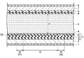
- FIG. 2 The figure which shows typically an example of a structure of the liquid crystal display element of this invention.
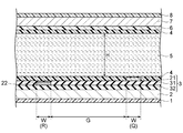
- FIG. 2 is a cross-sectional view of the liquid crystal display element shown in FIG. 1 taken along the line III-III in FIG.
- the figure which shows typically the orientation direction of the liquid crystal induced by the orientation film 4 An enlarged plan view of the electrode configuration of a liquid crystal display element Sectional drawing of the other example which cut
- the present invention has found a VA mode and IPS mode liquid crystal display element having a specific n-type liquid crystal composition and a specific element configuration.
- n-type means that ⁇ is negative.
- R i1 , R ii1 , R iii1 , R iii2 , R iv1 , R iv2 , R v1 , R v2 , R vi1 and R vi2 are preferably linear alkyl groups having 1 to 8 carbon atoms, methyl group, ethyl group , A propyl group, a butyl group and a pentyl group are preferred, and an ethyl group, a propyl group, a butyl group and a pentyl group are preferred.
- R i2 and R ii2 are preferably a straight-chain alkyl group having 1 to 5 carbon atoms or a straight-chain alkoxy group having 1 to 5 carbon atoms, such as methyl, ethyl, propyl, butyl, pentyl, methoxy Group, ethoxy group, propoxy group, butoxy group or pentoxy group is preferred.
- the compound represented by the general formula (i) can be used alone, or two or more compounds can be used in combination. There are no particular restrictions on the types of compounds that can be combined, but they are used in appropriate combinations according to the required properties such as solubility at low temperatures, transition temperatures, electrical reliability, and birefringence.
- the kind of the compound used is, for example, one kind as one embodiment of the present invention, two kinds, three kinds, four kinds, and five kinds or more.
- One compound of the general formula (i) and two compounds of the general formula (ii) are preferred, two compounds of the general formula (i) and two compounds of the general formula (ii) are represented.
- One type is preferable, two types of compounds of general formula (i) and two types of compounds of general formula (ii) are preferable.
- the lower limit of the preferable content of the compound represented by the formula (i) with respect to the total amount of the composition of the present invention is 5%, 7%, 9%, 11%, 13 %, 15%, and 17%.
- the upper limit value of the preferable content is 23%, 20%, 18%, 15%, 13%, and 11% with respect to the total amount of the composition of the present invention.
- the compound represented by the general formula (i) is preferably a compound selected from the group of compounds represented by the formulas (i.1) to (i.14). It is preferable that it is a compound represented by (i.5), and the compound represented by Formula (i.2), Formula (i.3), and Formula (i.5) is preferable.
- the compounds represented by the formulas (i.1) to (i.14) can be used alone or in combination, but they can be used alone or with respect to the total amount of the composition of the present invention.
- the lower limit of the preferable content of the compound is 3%, 5%, and 7%.
- the upper limit of the preferable content is 15%, 13%, 11%, 10%, and 9% with respect to the total amount of the composition of the present invention.
- the preferred total content of these compounds Is 5%, 7%, 9%, 11%, 13%, 15%, and 17%.
- the upper limit of the preferable content is 25%, 23%, 20%, 18%, 15%, 13%, and 11% with respect to the total amount of the composition of the present invention. %.
- the compound represented by the general formula (ii) can be used alone, or two or more compounds can be used in combination. There are no particular restrictions on the types of compounds that can be combined, but they are used in appropriate combinations according to the required properties such as solubility at low temperatures, transition temperatures, electrical reliability, and birefringence.
- the kind of the compound used is, for example, one kind as one embodiment of the present invention, two kinds, three kinds, four kinds, and five kinds or more.
- the lower limit of the preferable content of the compound represented by the formula (ii) with respect to the total amount of the composition of the present invention is 10%, 13%, 15%, 17%, 20 %, 23%, 25%, 27%, 30%, 33%, and 35%.
- the upper limit of the preferable content is 40%, 37%, 35%, 33%, and 30% with respect to the total amount of the composition of the present invention.
- the compound represented by the general formula (ii) is preferably a compound selected from the group of compounds represented by the formulas (ii.1) to (ii.15), and the compounds represented by the formulas (ii.1) to It is preferable that it is a compound represented by (ii.15), and the compound represented by Formula (ii.2) and Formula (ii.4) is preferable.
- the compounds represented by formula (ii.2) and formula (ii.4) can be used singly or in combination, either alone or with respect to the total amount of the composition of the present invention.
- the lower limit of the preferred content of these compounds is 10%, 13%, 15%, 17%, 20%, 23%, 25%, 27% , 30%, 33%, and 35%.
- the upper limit of the preferable content is 40%, 37%, 35%, 33%, and 30% with respect to the total amount of the composition of the present invention.
- the compound represented by the general formula (iii) can be used alone, but two or more compounds can be used in combination. There are no particular restrictions on the types of compounds that can be combined, but they are used in appropriate combinations according to the required properties such as solubility at low temperatures, transition temperatures, electrical reliability, and birefringence.
- the kind of the compound used is, for example, one kind as one embodiment of the present invention, two kinds, three kinds, four kinds, and five kinds or more.
- the lower limit of the preferable content is 1%, 2%, 3%, 5%, 7%, 10%, and 15% with respect to the total amount of the composition of the present invention. %, 18%, 20%, 22%, 25%, 28%, 30%.
- the upper limit of the preferable content is 45%, 43%, 40%, 38%, 35%, 33%, and 30% with respect to the total amount of the composition of the present invention. %.
- the lower limit value is high and the upper limit value is preferably high. Furthermore, when the composition of the present invention requires a high Tni and a composition having good temperature stability, it is preferable that the lower limit value is moderate and the upper limit value is moderate. When it is desired to increase the dielectric anisotropy in order to keep the driving voltage low, it is preferable that the lower limit value is low and the upper limit value is low.
- the compound represented by the general formula (iii) is preferably a compound selected from the group of compounds represented by the formula (iii.1) to the formula (iii.4), and the formula (iii.1), A compound represented by formula (iii.3) or formula (iii.4) is preferable.
- the compound represented by the formula (iii.1) is preferable because the response speed of the composition of the present invention is particularly improved.
- the lower limit of the preferable content of the compound represented by the formula (iii.1) with respect to the total amount of the composition of the present invention is 1%, 2%, 3%, 5% 7%, 10%, 13%, 15%, 18%, 20%.
- the upper limit of the preferable content is 20%, 17%, 15%, 13%, 10%, 8%, and 7% with respect to the total amount of the composition of the present invention. % And 6%.
- the compound represented by the formula (iii.1) is preferably 20% or less, preferably 10% or less, preferably 5% or less, and preferably not contained.
- the lower limit of the preferable total content of the compounds represented by formula (iii.3) or formula (iii.4) is 1%, 2%, 3%, 5%, 7 %, 10%, 13%, 15%, 18%, and 20%.
- the upper limit of the preferable content is 30%, 27%, 25%, 23%, 20%, 17%, and 15% with respect to the total amount of the composition of the present invention. %, 13%, 10%, 8%, 7%, 6%.
- the compound represented by the formula (iii.1) is mainly used, and the formula It is preferable to add a small amount of the compound represented by (iii.3) or formula (iii.4), and when the purpose is to improve the volatility of the compound represented by formula (iii.1) It is preferable to use mainly the compound represented by formula (iii.3) or formula (iii.4).
- the compound represented by the general formula (iv) can be used alone or in combination of two or more compounds. There are no particular restrictions on the types of compounds that can be combined, but they are used in appropriate combinations according to the required properties such as solubility at low temperatures, transition temperatures, electrical reliability, and birefringence.
- the kind of the compound used is, for example, one kind as one embodiment of the present invention, two kinds, three kinds, four kinds, and five kinds or more.
- the lower limit of the preferable content of the compound represented by the formula (iv) with respect to the total amount of the composition of the present invention is 5%, 7%, 10%, 13%, 15 %.
- the upper limit of the preferable content is 25%, 23%, 20%, 17%, 15%, 13%, and 10% with respect to the total amount of the composition of the present invention. % And 8%.
- the effect is high when the content is set to be large.
- the effect is high when the content is set low.
- the compound represented by the general formula (iv) is preferably a compound selected from the group of compounds represented by the formula (iv.1) or the formula (iv.2).
- the lower limit of the preferable total content of the compounds represented by formula (iv.1) or formula (iv.2) is 5%, 7%, 10%, 13%, 15 %.
- the upper limit of the preferable content is 25%, 23%, 20%, 17%, 15%, 13%, and 10% with respect to the total amount of the composition of the present invention. % And 8%.
- the compound represented by the general formula (v) can be used alone, or two or more compounds can be used in combination. There are no particular restrictions on the types of compounds that can be combined, but they are used in appropriate combinations according to the required properties such as solubility at low temperatures, transition temperatures, electrical reliability, and birefringence.
- the kind of the compound used is, for example, one kind as one embodiment of the present invention, two kinds, three kinds, four kinds, and five kinds or more.
- the content of the compound represented by the general formula (v) is low temperature solubility, transition temperature, electrical reliability, birefringence, process compatibility, dripping marks, image sticking, It is necessary to appropriately adjust according to required performance such as dielectric anisotropy.
- the lower limit of the preferable content of the compound represented by the formula (v) with respect to the total amount of the composition of the present invention is 1%, 2%, 3%, 5%, 7 % And 10%.
- the upper limit of the preferable content of the compound represented by the formula (v) with respect to the total amount of the composition of the present invention is 15%, 13%, 10%, 8%, 5% %.
- the compound represented by the general formula (v) is preferably a compound represented by the formula (v.1) to the formula (v.3), for example, and is a compound represented by the formula (v.1). It is preferable.
- the lower limit of the preferable content of the compound represented by the formula (v.1) with respect to the total amount of the composition of the present invention is 3%, 5%, 7%, 9%. 11%, 12%, 13%, 18%, 21%.
- Preferred upper limit values are 45, 40%, 35%, 30%, 25%, 23%, 20%, 18%, 15%, 13% %, 10%, and 8%.
- the compound represented by the general formula (vi) can be used alone, or two or more compounds can be used in combination. There are no particular restrictions on the types of compounds that can be combined, but they are used in appropriate combinations according to the required properties such as solubility at low temperatures, transition temperatures, electrical reliability, and birefringence.
- the kind of the compound used is, for example, one kind as one embodiment of the present invention, two kinds, three kinds, four kinds, and five kinds or more.
- the content of the compound represented by the general formula (vi) is low-temperature solubility, transition temperature, electrical reliability, birefringence, process compatibility, dripping marks, image sticking, It is necessary to appropriately adjust according to required performance such as dielectric anisotropy.
- the lower limit of the preferable content of the compound represented by the formula (vi) with respect to the total amount of the composition of the present invention is 1%, 2%, 3%, 5%, 7 %, 10%, 14%, 16%, 20%, 23%, 26%, 30%, 35%, and 40%.
- the upper limit of the preferable content of the compound represented by the formula (vi) with respect to the total amount of the composition of the present invention is 50%, 40%, 35%, 30%, 20 %, 15%, 10%, and 5%
- the compound represented by the general formula (vi) is a compound represented by the formula (vi.1) or the formula (vi.2). In particular, a compound represented by the formula (vi.1) is preferable.
- the lower limit of the preferable content of these compounds with respect to the total amount of the composition of the present invention is 1%, 2%, 3%, 5%, and 7%.
- the upper limit of the preferable content of these compounds is 20%, 15%, 13%, 10%, and 9%.
- the lower limit of the preferable total content of the compound represented by the general formula (i) and the compound represented by the general formula (ii) with respect to the total amount of the composition of the present invention is 30% and 35% 38% and 40%.
- the upper limit of the preferable content is 50%, 47%, 45%, 43%, 40%, and 37% with respect to the total amount of the composition of the present invention.
- the compound represented by the general formula (iii) the compound represented by the general formula (iv), the compound represented by the general formula (v) and the general formula (vi) with respect to the total amount of the composition of the present invention.
- the lower limit of the preferable total content of the represented compounds is 30%, 35%, 38%, and 40%.
- the upper limit of the preferable content is 50%, 47%, 45%, 43%, 40%, and 37% with respect to the total amount of the composition of the present invention.
- the lower limit of the preferable total content of the compound represented by the general formula (i) and the compound represented by the general formula (iv) with respect to the total amount of the composition of the present invention is 10%, 13% 15% and 17%.
- the upper limit of the preferable content is 35%, 33%, 30%, 28%, 25%, 24%, and 22% with respect to the total amount of the composition of the present invention. %, 20% and 18%.
- the lower limit of the preferable total content of the compound represented by the general formula (v) and the compound represented by the general formula (vi) with respect to the total amount of the composition of the present invention is 7%, 10% 13% and 15%.
- the upper limit of the preferable content is 30%, 27%, 25%, 23%, and 20% with respect to the total amount of the composition of the present invention.
- the compound represented by the general formula (i), the compound represented by the general formula (ii), the compound represented by the general formula (iii), and the general formula (iv) with respect to the total amount of the composition of the present invention is 80%, 83%, and 85%. Yes, 87%, 90%, 93%, 95%, 97%, 98%, 99%.
- the upper limit of the preferred content is 97% with respect to the total amount of the composition of the present invention, which is substantially free of other liquid crystal compounds as the liquid crystal compound except for the stabilizer and the polymerizable compound, etc. 95%, 93%, and 90%.
- the compound represented by the general formula (i) the compound represented by the general formula (ii), the compound represented by the general formula (iii), the compound represented by the general formula (iv), the general formula (v)
- the preferred lower limit of the total content of these compounds is 10%, 7%, 5% It is preferably 3% and substantially not contained.
- the liquid crystal compound other than the compound represented by the formula and the general formula (vi) include the following compounds.
- the compound represented by the formula (3CCV) or the formula (3CCV1) or the formula (2CCV1) is contained at 10% or less. It is preferable to make it contain in% or less and not to contain. When it is desired to improve image sticking, dripping marks, and volatility, the compound of formula (3CCV) is preferably contained at 10% or less, 5% or less, or not contained.
- R N111 and R N112 each independently represent an alkyl group having 1 to 8 carbon atoms or an alkoxy group having 1 to 8 carbon atoms.
- R N121 and R N122 each independently represent an alkyl group having 1 to 8 carbon atoms or an alkoxy group having 1 to 8 carbon atoms.
- R N131 and R N132 each independently represent an alkyl group having 1 to 8 carbon atoms or an alkoxy group having 1 to 8 carbon atoms.
- R N151 and R N152 each independently represent an alkyl group having 1 to 8 carbon atoms or an alkoxy group having 1 to 8 carbon atoms.
- R N1101 and R N1102 each independently represent an alkyl group having 1 to 8 carbon atoms or an alkoxy group having 1 to 8 carbon atoms
- R L21 and R L22 each independently represent an alkyl group having 1 to 8 carbon atoms or an alkoxy group having 1 to 8 carbon atoms.
- R L21 is preferably an alkyl group having 1 to 5 carbon atoms or an alkenyl group having 2 to 5 carbon atoms
- R L22 is an alkyl group having 1 to 5 carbon atoms, an alkenyl group having 4 to 5 carbon atoms, or a carbon atom.
- An alkoxy group of 1 to 4 is preferable.
- the compound represented by the general formula (L-1) can be used alone, or two or more compounds can be used in combination. There are no particular restrictions on the types of compounds that can be combined, but they are used in appropriate combinations according to the required properties such as solubility at low temperatures, transition temperatures, electrical reliability, and birefringence.
- the kind of the compound used is, for example, one kind as one embodiment of the present invention, two kinds, three kinds, four kinds, and five kinds or more.
- the lower limit of the preferable content of the compound represented by the formula (L-2) with respect to the total amount of the composition of the present invention is 1%, 2%, 3%, 5% 7% and 10%.
- the upper limit of the preferable content is 20%, 15%, 13%, 10%, 8%, 7%, and 6% with respect to the total amount of the composition of the present invention. %, 5%, 3%.
- the compound represented by the general formula (L-2) is preferably a compound selected from the group of compounds represented by the formulas (L-2.1) to (L-2.6).
- a compound represented by formula (L-2.1), formula (L-2.3), formula (L-2.4) and formula (L-2.6) is preferred.
- Compound represented by general formula (i), compound represented by general formula (ii), compound represented by general formula (N-1-1), general formula with respect to the total amount of the composition of the present invention A compound represented by (N-1-2), a compound represented by formula (N-1-3), a compound represented by formula (N-1-5), a compound represented by formula (N-1-
- the lower limit of the preferable total content of the compound represented by 10) is 30%, 32%, 35%, 38%, 40%, 42%, 43% 44%, 45%, 46%.
- the upper limit of the preferable content is 70%, 68%, 65%, 63%, 62%, 60%, 58%, 55%, 53% 52%, 50%, 48%.
- the compound represented by the general formula (iii), the compound represented by the general formula (iv), the compound represented by the general formula (v), and the general formula (vi) with respect to the total amount of the composition of the present invention is 35%, 38%, 40%, 42%, 43% 44%, 45%, 46%, 48%, 50%, 52%, 53%.
- the upper limit of the preferable content is 75%, 73%, 70%, 68%, 65%, 63%, 62%, 60%, 58% And 55%.
- the lower limit of the preferable total content of the compound and the compound represented by the general formula (L-2) is 80%, 85%, 88%, 90%, 92%, 93%, 94%, 95%, 96%, 97%, 98%, 99%, 100%.
- the upper limit of the preferable content is 100%, 99%, 98%, and 95%.
- the compound represented by the general formula (i), the compound represented by the general formula (ii), the compound represented by the general formula (iii), and the general formula (iv) with respect to the total amount of the composition of the present invention is: 80%, 85%, 88%, 90%, 92%, 93%, 94%, 95%, 96%, 97%, 98%, 99% and 100%.
- the upper limit of the preferable content is 100%, 99%, 98%, and 95%.
- composition of the present invention preferably does not contain a compound having a structure in which oxygen atoms such as a peracid (—CO—OO—) structure are bonded in the molecule.
- the content of the compound having a carbonyl group is preferably 5% or less, more preferably 3% or less with respect to the total mass of the composition. Preferably, it is more preferably 1% or less, and most preferably not substantially contained.
- the content of the compound substituted with chlorine atoms is preferably 15% or less, preferably 10% or less, based on the total mass of the composition. % Or less, preferably 5% or less, more preferably 3% or less, and still more preferably substantially not contained.
- the content of a compound whose ring structure in the molecule is a 6-membered ring
- the content of the compound whose ring structure in the molecule is a 6-membered ring is 80 % Or more, more preferably 90% or more, still more preferably 95% or more
- the composition is composed only of a compound in which all of the ring structures in the molecule are all 6-membered rings. Most preferably.
- the content of the compound having a cyclohexenylene group as a ring structure, and the content of the compound having a cyclohexenylene group as the total mass of the composition is preferably 10% or less, preferably 8% or less, more preferably 5% or less, preferably 3% or less, and still more preferably not contained.
- the content of a compound having a 2-methylbenzene-1,4-diyl group in the molecule, in which a hydrogen atom may be substituted with a halogen may be reduced.
- the content of the compound having a 2-methylbenzene-1,4-diyl group in the molecule is preferably 10% or less, more preferably 8% or less, based on the total mass of the composition. It is more preferably 5% or less, further preferably 3% or less, and still more preferably substantially not contained.
- substantially not contained in the present application means that it is not contained except for an unintentionally contained product.
- the alkenyl group when the compound contained in the composition of the first embodiment of the present invention has an alkenyl group as a side chain, when the alkenyl group is bonded to cyclohexane, the alkenyl group has 2 to 5 carbon atoms.
- the alkenyl group is bonded to benzene, the number of carbon atoms of the alkenyl group is preferably 4 to 5, and the unsaturated bond of the alkenyl group and benzene are directly bonded. Preferably not.
- the average elastic constant (K AVG ) of the liquid crystal composition used in the present invention is preferably 10 to 25, and the lower limit thereof is preferably 10, preferably 10.5, preferably 11 and preferably 11.5.
- 12 is preferable, 12.3 is preferable, 12.5 is preferable, 12.8 is preferable, 13 is preferable, 13.3 is preferable, 13.5 is preferable, 13.8 is preferable, 14 is preferable, 14 .3 is preferred, 14.5 is preferred, 14.8 is preferred, 15 is preferred, 15.3 is preferred, 15.5 is preferred, 15.8 is preferred, 16 is preferred, 16.3 is preferred, 16 .5, 16.8 is preferable, 17 is preferable, 17.3 is preferable, 17.5 is preferable, 17.8 is preferable, and 18 is preferable.
- 25 is preferable, 24.5 is preferable, 24 is preferable, 23.5 is preferable, 23 is preferable, 22.8 is preferable, 22.5 is preferable, 22.3 is preferable, 22 is preferable, and 21.8 is 21.5 is preferred, 21.3 is preferred, 21 is preferred, 20.8 is preferred, 20.5 is preferred, 20.3 is preferred, 20 is preferred, 19.8 is preferred, 19.5 is preferred 19.3 is preferred, 19 is preferred, 18.8 is preferred, 18.5 is preferred, 18.3 is preferred, 18 is preferred, 17.8 is preferred, 17.5 is preferred, 17.3 is preferred 17 is preferable.
- the value of K AVG should be set low. preferable. It is preferable to set a higher value of K AVG in the case of emphasizing improved response speed.
- the composition of the present invention may contain a polymerizable compound in order to produce a liquid crystal display element such as a PS mode, a transverse electric field type PSA mode, or a transverse electric field type PSVA mode.
- a polymerizable compound such as a PS mode, a transverse electric field type PSA mode, or a transverse electric field type PSVA mode.
- the polymerizable compound that can be used include a photopolymerizable monomer that undergoes polymerization by energy rays such as light.
- the structure has, for example, a liquid crystal skeleton in which a plurality of six-membered rings such as biphenyl derivatives and terphenyl derivatives are connected. Examples thereof include a polymerizable compound. More specifically, the general formula (XX)
- Z 201 represents —OCH 2 —, —CH 2 O—, —COO—, —OCO—, —CF 2 O—, —OCF 2 —, —CH 2 CH 2 —, —CF 2 CF 2 —, —CH ⁇ CH—COO—, —CH ⁇ CH—OCO—, —COO—CH ⁇ CH—, —OCO—CH ⁇ CH—, —COO—CH 2 CH 2 —, —OCO—CH 2 CH 2 —, —CH 2 CH 2 —COO—, —CH 2 CH 2 —, —OCO—CH 2 CH 2 —, —CH 2 CH 2 —COO—, —CH 2 CH 2 —OCO—, —COO—CH 2 CH 2 —, —OCO—CH 2 CH 2 —, —CH 2 CH 2 —COO—, —CH 2 CH 2 —OCO—, —COO—CH 2 CH 2 —, —OCO—CH 2 CH
- X 201 and X 202 are each preferably a diacrylate derivative that represents a hydrogen atom, or a dimethacrylate derivative that has a methyl group, and a compound in which one represents a hydrogen atom and the other represents a methyl group.
- diacrylate derivatives are the fastest, dimethacrylate derivatives are slow, asymmetric compounds are in the middle, and a preferred embodiment can be used depending on the application.
- a dimethacrylate derivative is particularly preferable.
- Sp 201 and Sp 202 each independently represent a single bond, an alkylene group having 1 to 8 carbon atoms, or —O— (CH 2 ) s —, but at least one of them is a single bond in a PSA display element.
- a compound in which both represent a single bond or one in which one represents a single bond and the other represents an alkylene group having 1 to 8 carbon atoms or —O— (CH 2 ) s — is preferable.
- 1 to 4 alkyl groups are preferable, and s is preferably 1 to 4.
- Z 201 represents —OCH 2 —, —CH 2 O—, —COO—, —OCO—, —CF 2 O—, —OCF 2 —, —CH 2 CH 2 —, —CF 2 CF 2 — or a single bond
- —COO—, —OCO— or a single bond is more preferred, and a single bond is particularly preferred.
- M 201 represents a 1,4-phenylene group, a trans-1,4-cyclohexylene group or a single bond in which any hydrogen atom may be substituted by a fluorine atom, but the 1,4-phenylene group or the single bond is preferable.
- C represents a ring structure other than a single bond
- Z 201 is preferably a linking group other than a single bond.
- M 201 is a single bond
- Z 201 is preferably a single bond.
- the ring structure between Sp 201 and Sp 202 is specifically preferably the structure described below.
- both ends shall be bonded to Sp 201 or Sp 202.
- the polymerizable compounds containing these skeletons are optimal for PSA-type liquid crystal display elements because of the alignment regulating power after polymerization, and a good alignment state can be obtained, so that display unevenness is suppressed or does not occur at all.
- general formula (XX-1) to general formula (XX-4) are particularly preferable, and among them, general formula (XX-2) is most preferable.
- benzene may be substituted with a fluorine atom
- Sp 20 represents an alkylene group having 2 to 5 carbon atoms.
- the polymerization proceeds even when no polymerization initiator is present, but may contain a polymerization initiator in order to accelerate the polymerization.
- the polymerization initiator include benzoin ethers, benzophenones, acetophenones, benzyl ketals, acylphosphine oxides, and the like.
- composition in the present invention can further contain a compound represented by the general formula (Q).
- RQ represents a straight-chain alkyl group or a branched-chain alkyl group having 1 to 22 carbon atoms, and one or more CH 2 groups in the alkyl group are —O—so that oxygen atoms are not directly adjacent to each other.
- MQ represents a trans-1,4-cyclohexylene group, a 1,4
- the compound represented by the general formula (Q) is preferably a compound represented by the following general formula (Qa) to general formula (Qd).
- R Q1 is preferably a linear or branched alkyl group having 1 to 10 carbon atoms
- R Q2 is preferably a linear or branched alkyl group having 1 to 20 carbon atoms
- R Q3 is A straight-chain alkyl group having 1 to 8 carbon atoms, a branched-chain alkyl group, a straight-chain alkoxy group or a branched-chain alkoxy group is preferred
- L Q is preferably a straight-chain alkylene group or branched-chain alkylene group having 1 to 8 carbon atoms.
- compounds represented by general formula (Qa) to general formula (Qd) compounds represented by general formula (Qc) and general formula (Qd) are more preferable.
- the compound represented by the general formula (Q) preferably contains one or two kinds, more preferably contains 1 to 5 kinds, and the content thereof is from 0.001. It is preferably 1%, more preferably 0.001 to 0.1%, and particularly preferably 0.001 to 0.05%.
- the polymerizable compound contained therein is polymerized by ultraviolet irradiation to impart liquid crystal alignment ability, and the amount of transmitted light is controlled using the birefringence of the composition.
- Used for liquid crystal display elements. Liquid crystal display element
- the liquid crystal composition of the present invention is applied to an IPS mode liquid crystal display device having the following constitution. An example of an IPS mode liquid crystal display device according to the present invention will be described with reference to FIGS.
- FIG. 1 is a diagram schematically showing a configuration of a liquid crystal display element.
- the configuration of the liquid crystal display element 10 according to the present invention is an IPS mode having a liquid crystal layer 5 sandwiched between a first substrate 2 and a second substrate 7 that are arranged opposite to each other.
- the liquid crystal layer 5 is composed of the liquid crystal composition of the present invention described above.
- the first substrate 2 has an electrode layer 3 formed on the surface on the liquid crystal layer 5 side. Further, between the liquid crystal layer 5 and each of the first substrate 2 and the second substrate 7, a pair of alignment films 4 that directly contact the liquid crystal composition constituting the liquid crystal layer 5 to induce homogeneous alignment are provided. The liquid crystal molecules in the liquid crystal composition are aligned so as to be substantially parallel to the first substrate 2 and the second substrate 7 when no voltage is applied. As shown in FIGS. 1 and 3, the first substrate 2 and the second substrate 7 may be sandwiched between a pair of polarizing plates 1 and 8. Further, as shown in FIG. 1, a color filter 6 may be provided between the second substrate 7 and the alignment film 4.
- the liquid crystal display element 10 includes a first polarizing plate 1, a first substrate 2, an electrode layer 3, an alignment film 4, a liquid crystal layer 5 containing a liquid crystal composition, an alignment film 4,
- the color filter 6, the second substrate 7, and the second polarizing plate 8 are sequentially stacked.
- the first substrate 2 and the second substrate 7 can be made of a flexible material such as glass or plastic, at least one of which is a transparent material and the other is a transparent material, such as metal or silicon. An opaque material may be used.
- the two substrates are bonded together by a sealing material and a sealing material such as an epoxy thermosetting composition disposed in the peripheral region, and in order to maintain the distance between the substrates, for example, glass particles, Spacer columns made of granular spacers such as plastic particles and alumina particles or a resin formed by photolithography may be arranged.
- a sealing material and a sealing material such as an epoxy thermosetting composition disposed in the peripheral region, and in order to maintain the distance between the substrates, for example, glass particles, Spacer columns made of granular spacers such as plastic particles and alumina particles or a resin formed by photolithography may be arranged.
- the first electrode and the second electrode are preferably transparent electrodes in order to improve the transmittance.
- the transparent electrode can be obtained by sputtering an oxide semiconductor (ZnO, InGaZnO, SiGe, GaAs, IZO (Indium Zinc Oxide), ITO (Indium Tin Oxide), SnO, TiO, AZTO (AlZnSnO)).
- the film thickness of the transparent electrode can be 10 to 200 nm.
- the amorphous ITO film can be changed to a polycrystalline ITO film, and the electrical resistance can be reduced.
- FIG. 2 is an enlarged plan view of a part of the region surrounded by the II line of the electrode layer 3 formed on the first substrate 2 in FIG.
- the electrode layer 3 including a thin film transistor formed on the surface of the first substrate 2 includes a plurality of gate bus lines 24 for supplying scanning signals and a plurality of data for supplying display signals.
- Bus lines 25 are arranged in a matrix so as to cross each other. In FIG. 2, only a pair of gate bus lines 24 and a pair of data bus lines 25 are shown.
- a unit pixel of the liquid crystal display device is formed by a region surrounded by the plurality of gate bus lines 24 and the plurality of data bus lines 25, and the first electrode 21 and the second electrode 22 are formed in the unit pixel. ing.
- a thin film transistor including a source electrode 27, a drain electrode 26, and a gate electrode 28 is provided in the vicinity of an intersection where the gate bus line 24 and the data bus line 25 intersect each other.
- the thin film transistor is connected to the first electrode 21 as a switch element that supplies a display signal to the first electrode 21.
- a common line 23 is provided in parallel with the gate bus line 24.
- the common line 23 is connected to the second electrode 22 in order to supply a common signal to the second electrode 22.
- the gate bus line 24, the data bus line 25, and the common line 23 are preferably metal films, more preferably Al, Cu, Au, Ag, Cr, Ta, Ti, Mo, W, Ni or alloys thereof, Mo, The case of using Al or its alloy wiring is particularly preferable.
- FIG. 3 is a cross-sectional view of the liquid crystal display element shown in FIG. 1 taken along the line III-III in FIG.
- a gate insulating layer 32 provided so as to cover the gate bus line 24 and cover substantially the entire surface of the first substrate 2, and an insulating protective layer 31 formed on the surface of the gate insulating layer 32.
- the line-shaped first electrode 21 and the line-shaped second electrode 22 are provided on the insulating protective film 31 so as to be separated from each other.
- the insulating protective layer 31 is a layer having an insulating function, and is formed of silicon nitride, silicon dioxide, silicon oxynitride film, or the like.
- the color filter 6 preferably forms a black matrix from the viewpoint of preventing light leakage, and preferably forms a black matrix (not shown) in a portion corresponding to the thin film transistor.
- the black matrix may be installed with the color filter on the substrate opposite to the array substrate, or may be installed with the color filter on the array substrate side.
- the black matrix is installed separately on the array substrate and the color filter is installed on the other substrate. May be.
- the black matrix may be provided separately from the color filter, but may be one that reduces the transmittance by overlapping each color of the color filter.
- the alignment film 4 is composed of, for example, a rubbed polyimide film.
- the polarizing plate 1 and the polarizing plate 8 can be adjusted so that the viewing angle and the contrast become good by adjusting the polarization axis of each polarizing plate so that their transmission axes operate in a normally black mode. It is preferable to have transmission axes perpendicular to each other.
- any one of the polarizing plate 1 and the polarizing plate 8 is preferably arranged so as to have a transmission axis parallel to the alignment direction of the liquid crystal molecules when no voltage is applied.
- the refractive index anisotropy ⁇ n of the liquid crystal composition is preferably adjusted according to the cell thickness d so that the contrast is maximized.
- a retardation film for widening the viewing angle can also be used.
- the first electrode 21 and the second electrode 22 are comb-shaped electrodes formed on the insulating protective layer 31, that is, on the same layer, and are engaged with each other at a distance. It is provided in the state.
- an interelectrode distance G between the first electrode 21 and the second electrode 22 and a thickness H of the liquid crystal layer sandwiched between the first substrate 2 and the second substrate 7 are G ⁇ H. Satisfy the relationship.
- the distance between electrodes: G represents the shortest distance in the horizontal direction on the substrate between the first electrode 21 and the second electrode 22, and in the example shown in FIGS. 2 and 3, the first electrode 21 and the second electrode 22 The distance in the vertical direction is expressed with respect to the line formed by alternately engaging the electrodes 22.
- H represents the shortest distance between the outermost surfaces of the first substrate 2 and the second substrate 7, specifically, The distance (that is, cell gap) between the alignment films 4 (outermost surfaces) provided on each of the first substrate 2 and the second substrate 7 represents the thickness of the liquid crystal layer as shown in FIG.
- the difference between the interelectrode distance G between the first electrode and the second electrode and the thickness H of the liquid crystal layer sandwiched between the first substrate and the second substrate is 0 ⁇ G ⁇ . It is preferable to satisfy the relationship of H ⁇ 0.5 ⁇ m.
- a liquid crystal composition having a large elastic constant is used, but by using the liquid crystal composition of the present invention and satisfying the relationship of 0 ⁇ GH ⁇ 0.5 ⁇ m, the driving voltage is reduced, Response speed can be further improved.
- GH is preferably greater than 0, preferably 0.5 or less, preferably 0.4 or less, preferably 0.3 or less, and preferably 0.2 or less. Preferably, it is 0.15 or less, and preferably 0.1 or less.
- the IPS type liquid crystal display element drives liquid crystal molecules by using an electric field in a horizontal direction with respect to a substrate surface formed between the first electrode 21 and the second electrode.
- the electrode width Q of the first electrode 21 and the electrode width R of the second electrode 22 are preferably formed to such a width that all the liquid crystal molecules in the liquid crystal layer 5 can be driven by the generated electric field.
- the electrode width W of at least one of the first electrode and the second electrode is preferably 3 ⁇ m or less, preferably 2.8 ⁇ m or less from the viewpoint of transmittance, and preferably 2.6 ⁇ m.
- the electrode width represents the width (line width) in the minor axis direction of a line formed by alternately engaging the first electrode 21 and the second electrode 22.
- the distance between the first electrode and the second electrode: G and the electrode width: W of at least one of the first electrode and the second electrode are such that GW ⁇ 3 ⁇ m. It is preferable to satisfy.
- the lower limit of GW is preferably 0 or more, preferably 0.1 or more, and preferably 0.1 or more. 0.2 or more, preferably 0.3 or more, and more preferably 0.5 or more.
- the upper limit is preferably 2.8 or less, preferably 2.5 or less, preferably 2.3 or less, preferably 2.0 or less, and 1.5 or less. Preferably, it is preferably 1.3 or less, preferably 1.2 or less, and preferably 1.1 or less.
- FIG. 4 is a diagram schematically showing the alignment direction of the liquid crystal induced by the alignment film 4.
- a liquid crystal composition having negative dielectric anisotropy is used. Therefore, the x axis and the major axis of the liquid crystal molecules 30 are defined with the x axis being the direction perpendicular to the line forming the comb shape of the first electrode 21 and the second electrode 22 (the direction in which the horizontal electric field is formed). Orientation is preferably made so that the angle ⁇ formed with the direction is approximately 0 to 45 °. In the example shown in FIG. 4, an example in which the angle ⁇ formed by the x axis and the major axis direction of the liquid crystal molecules 30 is approximately 0 ° is shown.
- the angle ⁇ formed by the x-axis and the major axis direction of the liquid crystal molecules 30 is preferably 0 to 40 °, more preferably 0 to 35 °, and even more preferably 0 to 30 ° C.
- the reason for inducing the alignment direction of the liquid crystal is to increase the maximum transmittance and contrast of the liquid crystal display device.
- the IPS-type liquid crystal display device 10 configured as described above supplies an image signal (voltage) to the first electrode 21 via the thin film TFT, whereby an electric field is generated between the first electrode 21 and the second electrode 22.
- the liquid crystal is driven by this electric field. That is, in a state where no voltage is applied, the liquid crystal molecules 30 are arranged so that the major axis direction thereof is parallel to the alignment direction of the alignment film 4.
- the liquid crystal molecules 30 in the liquid crystal layer 5 in accordance with the applied voltage are inclined such that the major axis direction of the liquid crystal molecules is constant with respect to the line in which the first electrodes 21 and the second electrodes 22 are alternately formed.
- the liquid crystal molecules 30 shown in FIG. 4 are schematically shown for explaining the movement of the liquid crystal molecules constituting the liquid crystal composition, and do not mean only specific liquid crystal molecules.
- FIG. 5 is an example showing another configuration of the first electrode 21 and the second electrode 22 formed in the pixel.
- FIG. 6 is another example in which the liquid crystal display element shown in FIG. 1 is cut in the direction of the line III-III in FIG.
- the second electrode 22 is provided on the gate insulating layer 32, the second electrode is mostly the insulating protective layer 31, the first electrode 21 is provided on the insulating protective layer 31, and the first electrode 21 is provided.
- the second electrode 22 may be provided on different layers.
- the liquid crystal display element of the present invention can form the electrode layer 3 by forming a wiring on the first substrate 2 by sputtering a metal material such as the electrode layer Al or its alloy.
- the color filter 6 can be prepared by, for example, a pigment dispersion method, a printing method, an electrodeposition method, a dyeing method, or the like. A method for producing a color filter by a pigment dispersion method will be described as an example.
- a curable coloring composition for a color filter is applied onto the transparent substrate, subjected to patterning treatment, and cured by heating or light irradiation. By performing this process for each of the three colors red, green, and blue, a pixel portion for a color filter can be created. Further, the color filter may be provided on the side of the substrate having a TFT or the like.
- the first substrate 2 and the second substrate 7 are opposed to each other so that the electrode layer 3 and the alignment film 4 side are on the inner side. At this time, the interval between the substrates may be adjusted via a spacer. In this case, it is preferable to adjust the thickness of the liquid crystal layer to be 1 to 100 ⁇ m.
- the thickness of the liquid crystal layer is preferably 1 to 20 ⁇ m, preferably 1 to 15 ⁇ m, preferably 1 to 10 ⁇ m, preferably 1.3 to 10 ⁇ m, preferably 1.5 to 10 ⁇ m, preferably 1.5 to 8 ⁇ m. 5 to 5 ⁇ m is preferable, 1.5 to 4 ⁇ m is preferable, 1.8 to 3.5 ⁇ m is preferable, and 2.0 to 3 ⁇ m is preferable.
- a polarizing plate When a polarizing plate is used, it is preferable to adjust the product of the refractive index anisotropy ⁇ n of the liquid crystal and the cell thickness d so that the contrast is maximized.
- the polarizing axis of each polarizing plate can be adjusted so that the viewing angle and contrast are good.
- a retardation film for widening the viewing angle can also be used.
- a sealant such as an epoxy thermosetting composition is screen-printed on the substrates with a liquid crystal inlet provided, the substrates are bonded together, and heated to thermally cure the sealant.
- a normal vacuum injection method or a drop injection (ODF: One Drop Fill) method can be used, but a drop mark is not generated in the vacuum injection method.
- ODF One Drop Fill
- it can be suitably used for a display element manufactured using the ODF method.
- a sealant such as epoxy photothermal combination curing is drawn on a backplane or frontplane substrate using a dispenser in a closed-loop bank shape, and then removed.
- a liquid crystal display element can be manufactured by bonding a front plane and a back plane after dropping a predetermined amount of the composition under air.
- a dripping mark is defined as a phenomenon in which a mark in which a liquid crystal composition is dripped appears white when displaying black.
- the occurrence of dripping marks is greatly affected by the liquid crystal material to be injected, but the influence is unavoidable depending on the configuration of the display element.
- the thin film transistor formed in the display element, the first electrode 21 having the comb shape or the slit, the second electrode 22, etc. are thinly aligned with the thin alignment film 4 or with the thin alignment film 4. Since there is only a protective layer 31 or the like that separates the liquid crystal composition, there is a high possibility that the ionic substance cannot be completely blocked, and avoiding the occurrence of dripping marks due to the interaction between the metal material constituting the electrode and the liquid crystal composition. However, by using the liquid crystal composition of the present invention in combination in an IPS type liquid crystal display element, the occurrence of dripping marks can be effectively suppressed.
- the liquid crystal display element in the manufacturing process of the liquid crystal display element by the ODF method, it is necessary to drop an optimal liquid crystal injection amount according to the size of the liquid crystal display element.
- the liquid crystal display element can be kept at a high yield because liquid crystal can be stably dropped over a long period of time with little influence on abrupt pressure change or impact in the apparatus.
- small liquid crystal display elements that are frequently used in smartphones that have been popular recently are difficult to control the deviation from the optimal value within a certain range because the optimal liquid crystal injection amount is small.
- a stable discharge amount of a liquid crystal material can be realized even in a small liquid crystal display element.
- the liquid crystal composition of the present invention contains a polymerizable compound
- an appropriate polymerization rate is desirable for obtaining a good alignment performance of the liquid crystal as a method for polymerizing the polymerizable compound, such as ultraviolet rays or electron beams.
- ultraviolet rays are used, a polarized light source or a non-polarized light source may be used.
- the polymerization is carried out in a state where the polymerizable compound-containing composition is sandwiched between two substrates, at least the substrate on the irradiated surface side must be given adequate transparency to the active energy rays. Don't be.
- the orientation state of the unpolymerized part is changed by changing conditions such as an electric field, a magnetic field, or temperature, and further irradiation with active energy rays is performed. Then, it is possible to use a means for polymerization.
- a means for polymerization In particular, when ultraviolet exposure is performed, it is preferable to perform ultraviolet exposure while applying an alternating electric field to the polymerizable compound-containing composition.
- the alternating electric field to be applied is preferably an alternating current having a frequency of 10 Hz to 10 kHz, more preferably a frequency of 60 Hz to 10 kHz, and the voltage is selected depending on a desired pretilt angle of the liquid crystal display element.
- the pretilt angle of the liquid crystal display element can be controlled by the applied voltage.
- the pretilt angle is preferably controlled from 80 degrees to 89.9 degrees from the viewpoint of alignment stability and contrast.
- the temperature at the time of irradiation is preferably within a temperature range in which the liquid crystal state of the composition of the present invention is maintained.
- Polymerization is preferably performed at a temperature close to room temperature, that is, typically at a temperature of 15 to 35 ° C.
- a lamp for generating ultraviolet rays a metal halide lamp, a high-pressure mercury lamp, an ultra-high pressure mercury lamp, or the like can be used.
- a wavelength of the ultraviolet-ray to irradiate it is preferable to irradiate the ultraviolet-ray of the wavelength range which is not the absorption wavelength range of a composition, and it is preferable to cut and use an ultraviolet-ray as needed.
- the intensity of the irradiated ultraviolet light is preferably 0.1 mW / cm 2 to 100 W / cm 2, more preferably 2 mW / cm 2 to 50 W / cm 2.
- the amount of energy of ultraviolet rays to be irradiated can be adjusted as appropriate, but is preferably 10 mJ / cm 2 to 500 J / cm 2, and more preferably 100 mJ / cm 2 to 200 J / cm 2.
- the intensity may be changed.
- the time for irradiating with ultraviolet rays is appropriately selected depending on the intensity of the irradiated ultraviolet rays, but is preferably from 10 seconds to 3600 seconds, and more preferably from 10 seconds to 600 seconds.
- the color filter can be prepared by, for example, a pigment dispersion method, a printing method, an electrodeposition method, or a dyeing method.
- a method for producing a color filter by a pigment dispersion method will be described as an example.
- a curable coloring composition for a color filter is applied onto the transparent substrate, subjected to patterning treatment, and cured by heating or light irradiation. By performing this process for each of the three colors red, green, and blue, a pixel portion for a color filter can be created.
- a pixel electrode provided with an active element such as a TFT, a thin film diode, or a metal insulator metal specific resistance element may be provided on the substrate.
- the substrate is opposed so that the transparent electrode layer is on the inside.
- the thickness of the obtained light control layer is 1 to 100 ⁇ m. More preferably, the thickness is 1.5 to 10 ⁇ m.
- the polarizing plate it is preferable to adjust the product of the refractive index anisotropy ⁇ n of the liquid crystal and the cell thickness d so that the contrast is maximized.
- the polarizing axis of each polarizing plate can be adjusted so that the viewing angle and contrast are good.
- a retardation film for widening the viewing angle can also be used.
- the spacer examples include columnar spacers made of glass particles, plastic particles, alumina particles, a photoresist material, and the like. Thereafter, a sealant such as an epoxy thermosetting composition is screen-printed on the substrates with a liquid crystal inlet provided, the substrates are bonded together, and heated to thermally cure the sealant.
- a sealant such as an epoxy thermosetting composition is screen-printed on the substrates with a liquid crystal inlet provided, the substrates are bonded together, and heated to thermally cure the sealant.
- a normal vacuum injection method or an ODF method can be used as a method for sandwiching the polymerizable compound-containing composition between the two substrates.
- a display element manufactured using the ODF method In the ODF liquid crystal display device manufacturing process, a sealant such as epoxy photothermal combination curing is drawn on a backplane or frontplane substrate using a dispenser in a closed-loop bank shape, and then removed.
- a liquid crystal display element can be manufactured by bonding a front plane and a back plane after dropping a predetermined amount of the composition under air.
- the composition of the present invention can be suitably used because the composition can be stably dropped in the ODF process.
- an appropriate polymerization rate is desirable in order to obtain good alignment performance of liquid crystals. Therefore, active energy rays such as ultraviolet rays or electron beams are irradiated singly or in combination or sequentially.
- the method of polymerizing by is preferred.
- ultraviolet rays When ultraviolet rays are used, a polarized light source or a non-polarized light source may be used.
- the polymerization is carried out in a state where the polymerizable compound-containing composition is sandwiched between two substrates, at least the substrate on the irradiated surface side must be given adequate transparency to the active energy rays. Don't be.
- the orientation state of the unpolymerized part is changed by changing conditions such as an electric field, a magnetic field, or temperature, and further irradiation with active energy rays is performed. Then, it is possible to use a means for polymerization.
- a means for polymerization In particular, when ultraviolet exposure is performed, it is preferable to perform ultraviolet exposure while applying an alternating electric field to the polymerizable compound-containing composition.
- the alternating electric field to be applied is preferably an alternating current having a frequency of 10 Hz to 10 kHz, more preferably a frequency of 60 Hz to 10 kHz, and the voltage is selected depending on a desired pretilt angle of the liquid crystal display element.
- the pretilt angle of the liquid crystal display element can be controlled by the applied voltage.
- the pretilt angle is preferably controlled from 80 degrees to 89.9 degrees from the viewpoint of alignment stability and contrast.
- the temperature at the time of irradiation is preferably within a temperature range in which the liquid crystal state of the composition of the present invention is maintained.
- Polymerization is preferably performed at a temperature close to room temperature, that is, typically at a temperature of 15 to 35 ° C.
- a lamp for generating ultraviolet rays a metal halide lamp, a high-pressure mercury lamp, an ultra-high pressure mercury lamp, or the like can be used.
- a wavelength of the ultraviolet-ray to irradiate it is preferable to irradiate the ultraviolet-ray of the wavelength range which is not the absorption wavelength range of a composition, and it is preferable to cut and use an ultraviolet-ray as needed.
- the intensity of the irradiated ultraviolet light is preferably 0.1 mW / cm 2 to 100 W / cm 2, more preferably 2 mW / cm 2 to 50 W / cm 2.
- the amount of energy of ultraviolet rays to be irradiated can be adjusted as appropriate, but is preferably 10 mJ / cm 2 to 500 J / cm 2, and more preferably 100 mJ / cm 2 to 200 J / cm 2.
- the intensity may be changed.
- the time for irradiating with ultraviolet rays is appropriately selected depending on the intensity of the irradiated ultraviolet rays, but is preferably from 10 seconds to 3600 seconds, and more preferably from 10 seconds to 600 seconds.
- the liquid crystal display element may be a method such as a vacuum injection method or a drop injection (ODF: One Drop Fill) method.
- ODF Drop injection
- a dripping mark is defined as a phenomenon in which a mark in which a liquid crystal composition is dripped appears white when displaying black.
- the occurrence of dripping marks is greatly affected by the liquid crystal material to be injected, but the influence is unavoidable depending on the configuration of the display element.
- the thin film transistor formed in the display element, the pixel electrode 21 having a comb shape or a slit, etc. are liquid crystal only in the thin alignment film 4 or the thin alignment film 4 and the thin insulating protective layer 18. Since there is no member that separates the composition, there is a high possibility that the ionic substance cannot be completely blocked, and the occurrence of dripping marks due to the interaction between the metal material constituting the electrode and the liquid crystal composition could not be avoided.
- the liquid crystal composition of the present invention in combination in the liquid crystal display element of the present invention, generation of dripping marks can be effectively suppressed.
- the liquid crystal display element in the manufacturing process of the liquid crystal display element by the ODF method, it is necessary to drop an optimal liquid crystal injection amount according to the size of the liquid crystal display element.
- the liquid crystal display element can be kept at a high yield because liquid crystal can be stably dropped over a long period of time with little influence on abrupt pressure change or impact in the apparatus.
- small liquid crystal display elements that are frequently used in smartphones that have been popular recently are difficult to control the deviation from the optimal value within a certain range because the optimal liquid crystal injection amount is small.
- a stable discharge amount of a liquid crystal material can be realized even in a small liquid crystal display element.
- n a natural number.
- the measured characteristics are as follows.
- T ni Nematic phase-isotropic liquid phase transition temperature (° C.)
- T ⁇ N Nematic phase lower limit temperature (° C)
- ⁇ n Refractive index anisotropy at 20 ° C.
- ⁇ Dielectric anisotropy at 20 ° C.
- ⁇ 1 Rotational viscosity at 20 ° C. (mPa ⁇ s)
- K 33 Elastic constant at 20 ° C.
- VHR VHR
- VHR Voltage holding ratio (%) at a frequency of 60 Hz, an applied voltage of 1 V, and 60 ° C.
- Burn-in Evaluation of burn-in of the liquid crystal display element shows that the fixed pattern afterimage reaches an unacceptable afterimage level when the entire fixed screen is displayed after displaying the specified fixed pattern in the display area for an arbitrary test time. The test time until was measured. 1) The test time referred to here indicates the display time of the fixed pattern, and the longer this time is, the more the afterimage is suppressed and the higher the performance. 2) The unacceptable afterimage level is a level at which an afterimage that is rejected in the shipment acceptance / rejection determination is observed.
- Sample A 1000 hours
- Sample B 500 hours
- Sample C 200 hours
- Sample D 100 hours Performance is A>B>C> D.
- Drop marks The evaluation of the drop marks of the liquid crystal display device was performed by visual observation of the drop marks that appeared white when the entire surface was displayed in black by the following five-step evaluation.
- Nematic phase stability at low temperature The nematic phase stability at low temperature was evaluated by weighing 1 g of the composition into a 2 mL sample bottle after preparing the composition, and then adding the following operating state “ ⁇ 20 ° C.
- Example 1 is a compound represented by the general formula (i) described in claim 1 of the present application, a compound represented by the general formula (ii), a compound represented by the general formula (iii), It is a composition containing a compound represented by the general formula (iv), a compound represented by the general formula (v) and a compound represented by the general formula (vi), and the content thereof is 96%. .
- composition shown as Comparative Example 1 reduced the content of the compound represented by the general formula (iii) and the compound represented by the general formula (iv) with respect to Example 1, CyCy-1 and V2-PhPh-1 are added, the compound represented by the general formula (i), the compound represented by the general formula (ii), the compound represented by the general formula (iii) in the composition,
- the total content of the compound represented by the general formula (iv), the compound represented by the general formula (v), and the compound represented by the general formula (vi) is 85%.
- composition shown as Comparative Example 2 reduced the content of the compound represented by the general formula (ii) and the compound represented by the general formula (iii) with respect to Example 1, and produced 3-Cy-1O.
- a compound represented by the general formula (iv), a compound represented by the general formula (v) and a total content of the compound represented by the general formula (vi) is 79%. It is a thing.
- the composition of Example 1 has various properties such as desired T ni , ⁇ , ⁇ 1 , nematic phase stability at low temperature, and has excellent image sticking, dripping marks, nematic stability at low temperature, and volatility. Therefore, a VA liquid crystal display element having a cell thickness of 3.2 ⁇ m was fabricated, the response speed was evaluated, and it was confirmed that the response was sufficiently fast. It was also confirmed that the high transmittance required for liquid crystal televisions was obtained. Moreover, when VHR (UV) of the VA type liquid crystal display element using the composition of Example 1, Comparative Example 1, Comparative Example 2, and Example 2 was evaluated, Example 1 and Example 2 had sufficiently high numerical values. Was confirmed to be highly reliable, but in Comparative Examples 1 and 2, a decrease in VHR (UV) was confirmed.
- VHR UV
- the composition of the present invention can be used at the time of production without deteriorating various characteristics as a liquid crystal display element such as T ni , ⁇ , ⁇ 1 , and nematic phase stability at low temperature, and image sticking characteristics of the display element. It has been found that a composition that hardly causes dripping marks and hardly volatilizes in the ODF process can be provided, and a liquid crystal display device using the composition has a high-speed response and high reliability.
Landscapes
- Chemical & Material Sciences (AREA)
- Crystallography & Structural Chemistry (AREA)
- Engineering & Computer Science (AREA)
- Materials Engineering (AREA)
- Organic Chemistry (AREA)
- Liquid Crystal Substances (AREA)
Abstract
[課題] 本発明が解決しようとする課題は、Tni、Δε、γ1、低温でのネマチック相安定性等の液晶表示素子としての諸特性及び表示素子の焼き付き特性を悪化させることなく、製造時の滴下痕が発生し難く、ODF工程において揮発し難い液晶組成物及びそれを用いた液晶表示素子を提供することにある。 [解決手段] 本発明者は、種々の液晶化合物及び種々の化学物質を検討し、特定の液晶化合物を組み合わせることにより前記課題を解決することができることを見出し、本発明を完成するに至った。 一般式(i)~(vi)で表される化合物を含有する組成物、当該組成物を使用した液晶表示素子及び当該組成物を使用したVA方式素子、FFS素子又はIPSを提供する。
Description
本発明は液晶表示材料として有用な誘電率異方性(Δε)が負の値を示す組成物及びこれを用いた液晶表示素子に関する。
Δεが負の値を示す組成物を用いた液晶表示素子は、液晶TV等に広く用いられており、これら用途に使用される組成物には高い特性が要求されている。例えば、高いネマチック相上限温度Tni、大きなΔε、低い回転粘性(γ1)、低温でのネマチック相安定性などの諸特性がある。さらに、表示素子の焼き付きなどの表示不良が発生し難い、製造時の滴下痕が発生し難い、ODF工程における組成物の安定した吐出性等の要求があり、従来の液晶組成物では対応できなくなってきている。
本発明が解決しようとする課題は、Tni、Δε、γ1、低温でのネマチック相安定性等の液晶表示素子としての諸特性及び表示素子の焼き付き特性を悪化させることなく、製造時の滴下痕が発生し難く、ODF工程において揮発し難い液晶組成物及びそれを用いた液晶表示素子を提供することにある。
本発明者は、種々の液晶化合物及び種々の化学物質を検討し、特定の液晶化合物を組み合わせることにより前記課題を解決することができることを見出し、本発明を完成するに至った。
一般式(i)~(vi)で表される化合物を含有する組成物、当該組成物を使用した液晶表示素子及び当該組成物を使用したVA(Virtical Alignment)方式素子、FFS(Fringe Field Switching)素子又はIPS(In Plane Switching)を提供する。
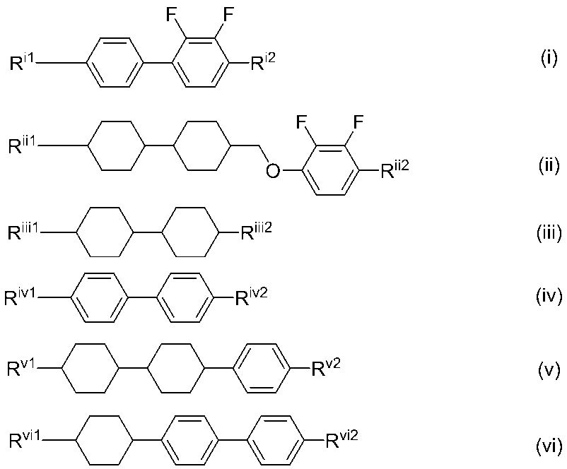
(式中、Ri1、Rii1、Riii1、Riii2、Riv1、Riv2、Rv1、Rv2、Rvi1及びRvi2はそれぞれ独立して、炭素原子数1~8のアルキル基を表し、Ri2及びRii2はそれぞれ独立して、炭素原子数1~8のアルキル基又は炭素原子数1~8のアルコキシ基を表す。)
本発明の負の誘電率異方性を有する組成物は、大幅に低い粘性を得ることができ、低温でのネマチック相安定性が良好で、加熱や光照射による比抵抗や電圧保持率の変化が極めて小さいため、製品の実用性と信頼性が高く、これを用いたVA方式やFFS方式等の液晶表示素子は所望の駆動電圧において高速応答を達成できる。また、本発明の液晶組成物は揮発し難いため、液晶表示素子の製造工程において安定的に性能を発揮でき、工程起因の表示不良が抑制されて歩留まり高く製造できるので、非常に有用である。
前述の通り、本願発明は、特定のn型液晶組成物と特定の素子構成を持つVA方式、IPS方式の液晶表示素子を見出したものである。ここでn型とはΔεが負を意味する。
以下、まず、本発明における液晶組成物の実施の態様について説明する。
以下、まず、本発明における液晶組成物の実施の態様について説明する。
Ri1、Rii1、Riii1、Riii2、Riv1、Riv2、Rv1、Rv2、Rvi1及びRvi2は直鎖の炭素原子数1~8のアルキル基が好ましく、メチル基、エチル基、プロピル基、ブチル基及びペンチル基が好ましく、エチル基、プロピル基、ブチル基及びペンチル基が好ましい。
Ri2及びRii2は直鎖の炭素原子数1~5のアルキル基又は直鎖の炭素原子数1~5のアルコキシ基が好ましく、メチル基、エチル基、プロピル基、ブチル基、ペンチル基、メトキシ基、エトキシ基、プロポキシ基、ブトキシ基又はペントキシ基が好ましい。
一般式(i)で表される化合物は単独で使用することもできるが、2以上の化合物を組み合わせて使用することもできる。組み合わせることができる化合物の種類に特に制限は無いが、低温での溶解性、転移温度、電気的な信頼性、複屈折率などの求められる性能に応じて適宜組み合わせて使用する。使用する化合物の種類は、例えば本発明の一つの実施形態としては1種類であり、2種類であり、3種類であり、4種類であり、5種類以上である。
Δεの改善を重視する場合には含有量を高めに設定することが好ましく、低温での溶解性を重視する場合は含有量を多めに設定すると効果が高く、Tniを重視する場合は含有量を少なめに設定すると効果が高い。さらに、滴下痕や焼き付き特性を改良する場合は、含有量の範囲を中間に設定することが好ましい。また、Δεを大きくすることで低電圧駆動が可能となるが、本発明の液晶組成物においては、一般式(i)の化合物および一般式(ii)の化合物を単独または組み合わせて使うことにより、低電圧かつ高速応答の液晶表示素子を得ることができる。この組み合わせについて詳述すると、一般式(i)の化合物を1種および一般式(ii)の化合物を2種が好ましく、一般式(i)の化合物を2種および一般式(ii)の化合物を1種が好ましく、一般式(i)の化合物を2種および一般式(ii)の化合物を2種が好ましい。
本発明の組成物の総量に対しての式(i)で表される化合物の好ましい含有量の下限値は、5%であり、7%であり、9%であり、11%であり、13%であり、15%であり、17%である。好ましい含有量の上限値は、本発明の組成物の総量に対して、23%であり、20%であり、18%であり、15%であり、13%であり、11%である。
さらに、一般式(i)で表される化合物は、式(i.1)から式(i.14)で表される化合物群から選ばれる化合物であることが好ましく、式(i.1)~(i.5)で表される化合物であることが好ましく、式(i.2)、式(i.3)及び式(i.5)で表される化合物が好ましい。
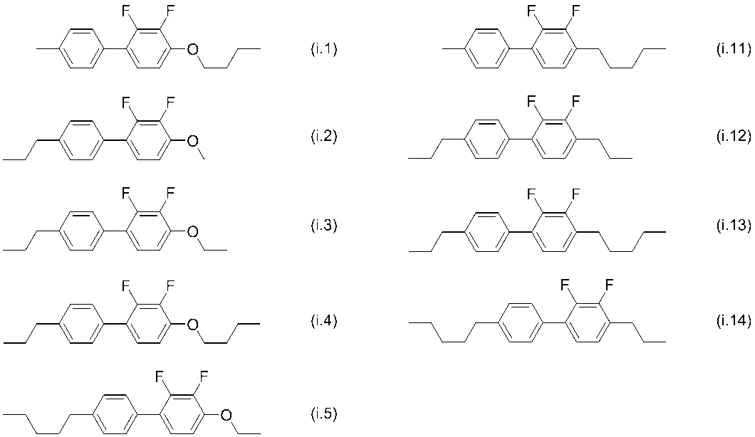
式(i.1)~(i.14)で表される化合物は単独で使用することも、組み合わせて使用することも可能であるが、本発明の組成物の総量に対しての単独又はこれら化合物の好ましい含有量の下限値は、3%であり、5%であり、7%である。好ましい含有量の上限値は、本発明の組成物の総量に対して、15%であり、13%であり、11%であり、10%であり、9%である。
式(i.2)、式(i.3)及び式(i.5)で表される化合物から選ばれる2種又は3種を組み合わせて使用する場合には、これら化合物の合計の好ましい含有量の下限値は、5%であり、7%であり、9%であり、11%であり、13%であり、15%であり、17%である。好ましい含有量の上限値は、本発明の組成物の総量に対して、25%であり、23%であり、20%であり、18%であり、15%であり、13%であり、11%である。
一般式(ii)で表される化合物は単独で使用することもできるが、2以上の化合物を組み合わせて使用することもできる。組み合わせることができる化合物の種類に特に制限は無いが、低温での溶解性、転移温度、電気的な信頼性、複屈折率などの求められる性能に応じて適宜組み合わせて使用する。使用する化合物の種類は、例えば本発明の一つの実施形態としては1種類であり、2種類であり、3種類であり、4種類であり、5種類以上である。
Δεの改善を重視する場合には含有量を高めに設定することが好ましく、低温での溶解性を重視する場合は含有量を低めに設定すると効果が高く、TNIを重視する場合は含有量を高めに設定すると効果が高い。さらに、滴下痕や焼き付き特性を改良する場合は、含有量の範囲を中間に設定することが好ましい。
本発明の組成物の総量に対しての式(ii)で表される化合物の好ましい含有量の下限値は、10%であり、13%であり、15%であり、17%であり、20%であり、23%であり、25%であり、27%であり、30%であり、33%であり、35%である。好ましい含有量の上限値は、本発明の組成物の総量に対して、40%であり、37%であり、35%であり、33%であり、30%である。
さらに、一般式(ii)で表される化合物は、式(ii.1)から式(ii.15)で表される化合物群から選ばれる化合物であることが好ましく、式(ii.1)~(ii.15)で表される化合物であることが好ましく、式(ii.2)及び式(ii.4)で表される化合物が好ましい。
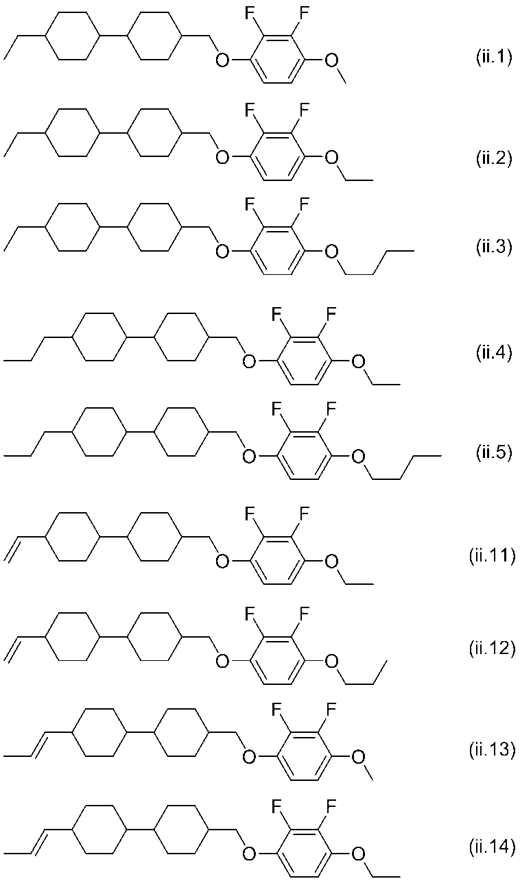
式(ii.2)及び式(ii.4)で表される化合物は単独で使用することも、組み合わせて使用することも可能であるが、本発明の組成物の総量に対しての単独又はこれら化合物の好ましい含有量の下限値は、10%であり、13%であり、15%であり、17%であり、20%であり、23%であり、25%であり、27%であり、30%であり、33%であり、35%である。好ましい含有量の上限値は、本発明の組成物の総量に対して、40%であり、37%であり、35%であり、33%であり、30%である。
一般式(iii)で表される化合物は単独で使用することもできるが、2以上の化合物を組み合わせて使用することもできる。組み合わせることができる化合物の種類に特に制限は無いが、低温での溶解性、転移温度、電気的な信頼性、複屈折率などの求められる性能に応じて適宜組み合わせて使用する。使用する化合物の種類は、例えば本発明の一つの実施形態としては1種類であり、2種類であり、3種類であり、4種類であり、5種類以上である。
好ましい含有量の下限値は、本発明の組成物の総量に対して、1%であり、2%であり、3%であり、5%であり、7%であり、10%であり、15%であり、18%であり、20%であり、22%であり、25%であり、28%であり、30%である。好ましい含有量の上限値は、本発明の組成物の総量に対して、45%であり、43%であり、40%であり、38%であり、35%であり、33%であり、30%である。
本発明の組成物の粘度を低く保ち、応答速度が速い組成物が必要な場合は上記の下限値が高く上限値が高いことが好ましい。さらに、本発明の組成物のTniを高く保ち、温度安定性の良い組成物が必要な場合は上記の下限値が中庸で上限値が中庸であることが好ましい。また、駆動電圧を低く保つために誘電率異方性を大きくしたいときは、上記の下限値が低く上限値が低いことが好ましい。
さらに、一般式(iii)で表される化合物は、式(iii.1)から式(iii.4)で表される化合物群から選ばれる化合物であることが好ましく、式(iii.1)、式(iii.3)又は式(iii.4)で表される化合物であることが好ましい。特に、式(iii.1)で表される化合物は本発明の組成物の応答速度を特に改善するため好ましい。また、応答速度よりも高いTniを求めるときは、式(iii.3)及び式(iii.4)で表される化合物を用いることが好ましいが、これら化合物の合計の含有量は、低温での溶解度を良くするために20%以上にすることは好ましくない。
さらに、一般式(iii)で表される化合物は、式(iii.1)から式(iii.4)で表される化合物群から選ばれる化合物であることが好ましく、式(iii.1)、式(iii.3)又は式(iii.4)で表される化合物であることが好ましい。特に、式(iii.1)で表される化合物は本発明の組成物の応答速度を特に改善するため好ましい。また、応答速度よりも高いTniを求めるときは、式(iii.3)及び式(iii.4)で表される化合物を用いることが好ましいが、これら化合物の合計の含有量は、低温での溶解度を良くするために20%以上にすることは好ましくない。

本発明の組成物の総量に対しての式(iii.1)で表される化合物の好ましい含有量の下限値は、1%であり、2%であり、3%であり、5%であり、7%であり、10%であり、13%であり、15%であり、18%であり、20%である。好ましい含有量の上限値は、本発明の組成物の総量に対して、20%であり、17%であり、15%であり、13%であり、10%であり、8%であり、7%であり、6%である。揮発性を改良することを重視する場合には、式(iii.1)で表される化合物は20%以下が好ましく、10%以下が好ましく、5%以下が好ましく、含有しないことが好ましい。
式(iii.3)又は式(iii.4)で表される化合物の合計の好ましい含有量の下限値は、1%であり、2%であり、3%であり、5%であり、7%であり、10%であり、13%であり、15%であり、18%であり、20%である。好ましい含有量の上限値は、本発明の組成物の総量に対して、30%であり、27%であり、25%であり、23%であり、20%であり、17%であり、15%であり、13%であり、10%であり、8%であり、7%であり、6%である。
一般式式(iii)で表される化合物を複数組み合わせて使用する場合に、応答速度の改善に重点を置く場合には、式(iii.1)で表される化合物を中心に使用し、式(iii.3)又は式(iii.4)で表される化合物を少量添加することが好ましく、式(iii.1)で表される化合物の揮発性を改善することを目的とする場合には、式(iii.3)又は式(iii.4)で表される化合物を中心に使用することが好ましい。
一般式(iv)で表される化合物は単独で使用することもできるが、2以上の化合物を組み合わせて使用することもできる。組み合わせることができる化合物の種類に特に制限は無いが、低温での溶解性、転移温度、電気的な信頼性、複屈折率などの求められる性能に応じて適宜組み合わせて使用する。使用する化合物の種類は、例えば本発明の一つの実施形態としては1種類であり、2種類であり、3種類であり、4種類であり、5種類以上である。
本発明の組成物の総量に対しての式(iv)で表される化合物の好ましい含有量の下限値は、5%であり、7%であり、10%であり、13%であり、15%である。好ましい含有量の上限値は、本発明の組成物の総量に対して、25%であり、23%であり、20%であり、17%であり、15%であり、13%であり、10%であり、8%である。
高い複屈折率を得る場合は含有量を多めに設定すると効果が高く、反対に、高いTniを重視する場合は含有量を少なめに設定すると効果が高い。さらに、滴下痕や焼き付き特性を改良する場合は、含有量の範囲を中間に設定することが好ましい。
さらに、一般式(iv)で表される化合物は、式(iv.1)又は式(iv.2)で表される化合物群から選ばれる化合物であることが好ましい。
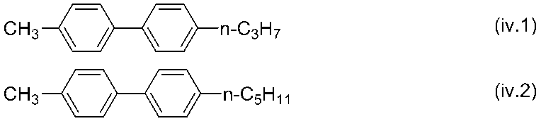
式(iv.1)又は式(iv.2)で表される化合物の合計の好ましい含有量の下限値は、5%であり、7%であり、10%であり、13%であり、15%である。好ましい含有量の上限値は、本発明の組成物の総量に対して、25%であり、23%であり、20%であり、17%であり、15%であり、13%であり、10%であり、8%である。
一般式(v)で表される化合物は単独で使用することもできるが、2以上の化合物を組み合わせて使用することもできる。組み合わせることができる化合物の種類に特に制限は無いが、低温での溶解性、転移温度、電気的な信頼性、複屈折率などの求められる性能に応じて適宜組み合わせて使用する。使用する化合物の種類は、例えば本発明の一つの実施形態としては1種類であり、2種類であり、3種類であり、4種類であり、5種類以上である。
本発明の組成物において、一般式(v)で表される化合物の含有量は、低温での溶解性、転移温度、電気的な信頼性、複屈折率、プロセス適合性、滴下痕、焼き付き、誘電率異方性などの求められる性能に応じて適宜調整する必要がある。
本発明の組成物の総量に対しての式(v)で表される化合物の好ましい含有量の下限値は、1%であり、2%であり、3%であり、5%であり、7%であり、10%である。本発明の組成物の総量に対しての式(v)で表される化合物の好ましい含有量の上限値は、15%であり、13%であり、10%であり、8%であり、5%である。
一般式(v)で表される化合物は、例えば式(v.1)から式(v.3)で表される化合物であることが好ましく、式(v.1)で表される化合物であることが好ましい。

低温での溶解性、転移温度、電気的な信頼性、複屈折率などの求められる性能に応じて、式(v.1)で表される化合物を含有していても、式(v.1)で表される化合物と式(v.2)で表される化合物との両方を含有していても良い。
本発明の組成物の総量に対しての式(v.1)で表される化合物の好ましい含有量の下限値は、3%であり、5%であり、7%であり、9%であり、11%であり、12%であり、13%であり、18%であり、21%である。好ましい上限値は、45であり、40%であり、35%であり、30%であり、25%であり、23%であり、20%であり、18%であり、15%であり、13%であり、10%であり、8%である。
一般式(vi)で表される化合物は単独で使用することもできるが、2以上の化合物を組み合わせて使用することもできる。組み合わせることができる化合物の種類に特に制限は無いが、低温での溶解性、転移温度、電気的な信頼性、複屈折率などの求められる性能に応じて適宜組み合わせて使用する。使用する化合物の種類は、例えば本発明の一つの実施形態としては1種類であり、2種類であり、3種類であり、4種類であり、5種類以上である。
本発明の組成物において、一般式(vi)で表される化合物の含有量は、低温での溶解性、転移温度、電気的な信頼性、複屈折率、プロセス適合性、滴下痕、焼き付き、誘電率異方性などの求められる性能に応じて適宜調整する必要がある。
本発明の組成物の総量に対しての式(vi)で表される化合物の好ましい含有量の下限値は、1%であり、2%であり、3%であり、5%であり、7%であり、10%であり、14%であり、16%であり、20%であり、23%であり、26%であり、30%であり、35%であり、40%である。本発明の組成物の総量に対しての式(vi)で表される化合物の好ましい含有量の上限値は、50%であり、40%であり、35%であり、30%であり、20%であり、15%であり、10%であり、5%である
一般式(vi)で表される化合物は、式(vi.1)又は式(vi.2)で表される化合物であることが好ましく、特に、式(vi.1)で表される化合物であることが好ましい。
一般式(vi)で表される化合物は、式(vi.1)又は式(vi.2)で表される化合物であることが好ましく、特に、式(vi.1)で表される化合物であることが好ましい。

本発明の組成物の総量に対してのこれら化合物の好ましい含有量の下限値は、1%であり、2%であり、3%であり、5%であり、7%である。これら化合物の好ましい含有量の上限値は、20%であり、15%であり、13%であり、10%であり、9%である。
本発明の組成物の総量に対しての一般式(i)で表される化合物及び一般式(ii)で表される化合物の好ましい合計の含有量の下限値は、30%であり、35%であり、38%であり、40%である。好ましい含有量の上限値は、本発明の組成物の総量に対して、50%であり、47%であり、45%であり、43%であり、40%であり、37%である。
本発明の組成物の総量に対しての一般式(iii)で表される化合物、一般式(iv)で表される化合物、一般式(v)で表される化合物及び一般式(vi)で表される化合物の好ましい合計の含有量の下限値は、30%であり、35%であり、38%であり、40%である。好ましい含有量の上限値は、本発明の組成物の総量に対して、50%であり、47%であり、45%であり、43%であり、40%であり、37%である。
本発明の組成物の総量に対しての一般式(i)で表される化合物及び一般式(iv)で表される化合物の好ましい合計の含有量の下限値は、10%であり、13%であり、15%であり、17%である。好ましい含有量の上限値は、本発明の組成物の総量に対して、35%であり、33%であり、30%であり、28%であり、25%であり、24%であり、22%であり、20%であり、18%である。
本発明の組成物の総量に対しての一般式(v)で表される化合物及び一般式(vi)で表される化合物の好ましい合計の含有量の下限値は、7%であり、10%であり、13%であり、15%である。好ましい含有量の上限値は、本発明の組成物の総量に対して、30%であり、27%であり、25%であり、23%であり、20%である。
本発明の組成物の総量に対しての一般式(i)で表される化合物、一般式(ii)で表される化合物、一般式(iii)で表される化合物、一般式(iv)で表される化合物、一般式(v)で表される化合物及び一般式(vi)で表される化合物の好ましい合計の含有量の下限値は、80%であり、83%であり、85%であり、87%であり、90%であり、93%であり、95%であり、97%であり、98%であり、99%である。好ましい含有量の上限値は、本発明の組成物の総量に対して、安定剤及び重合性化合物等を除き液晶化合物のみとして実質的に他の液晶性化合物を含有しないか、97%であり、95%であり、93%であり、90%である。
一般式(i)で表される化合物、一般式(ii)で表される化合物、一般式(iii)で表される化合物、一般式(iv)で表される化合物、一般式(v)で表される化合物及び一般式(vi)で表される化合物以外の液晶化合物を含んでいても良いがそれら化合物の合計の含有量の好ましい下限値は10%であり、7%であり、5%であり、3%であり、実質的に含有しないことが好ましい。
一般式(i)で表される化合物、一般式(ii)で表される化合物、一般式(iii)で表される化合物、一般式(iv)で表される化合物、一般式(v)で表される化合物及び一般式(vi)で表される化合物以外の液晶化合物としては下記の化合物がある。
式(3CCV)または式(3CCV1)または式(2CCV1)で表される化合物。
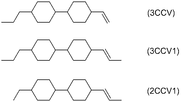
加熱や光照射による電圧保持率(VHR)の変化を抑制したい場合には、式(3CCV)または式(3CCV1)または式(2CCV1)で表される化合物は、10%以下で含有させるか、5%以下で含有させるか、含有しないことが好ましい。また、焼き付き、滴下痕、揮発性を改良したい場合には、式(3CCV)の化合物は、10%以下で含有させるか、5%以下で含有させるか、含有しないことが好ましい。
一般式(N-1-1)で表される化合物。
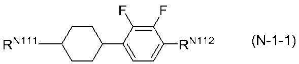
(式中、RN111及びRN112はそれぞれ独立して、炭素原子数1~8のアルキル基又は炭素原子数1~8のアルコキシ基を表す。)
一般式(N-1-2)で表される化合物。
一般式(N-1-2)で表される化合物。

(式中、RN121及びRN122はそれぞれ独立して、炭素原子数1~8のアルキル基又は炭素原子数1~8のアルコキシ基を表す。)
一般式(N-1-3)で表される化合物。
一般式(N-1-3)で表される化合物。

(式中、RN131及びRN132はそれぞれ独立して、炭素原子数1~8のアルキル基又は炭素原子数1~8のアルコキシ基を表す。)
一般式(N-1-5)で表される化合物。
一般式(N-1-5)で表される化合物。

(式中、RN151及びRN152はそれぞれ独立して、炭素原子数1~8のアルキル基又は炭素原子数1~8のアルコキシ基を表す。)
一般式(N-1-10)で表される化合物。
一般式(N-1-10)で表される化合物。

(式中、RN1101及びRN1102はそれぞれ独立して、炭素原子数1~8のアルキル基又は炭素原子数1~8のアルコキシ基を表す。)
一般式(L-2)で表される化合物。
一般式(L-2)で表される化合物。

(式中、RL21及びRL22はそれぞれ独立して、炭素原子数1~8のアルキル基又は炭素原子数1~8のアルコキシ基を表す。)
RL21は炭素原子数1~5のアルキル基又は炭素原子数2~5のアルケニル基が好ましく、RL22は炭素原子数1~5のアルキル基、炭素原子数4~5のアルケニル基又は炭素原子数1~4のアルコキシ基が好ましい。
RL21は炭素原子数1~5のアルキル基又は炭素原子数2~5のアルケニル基が好ましく、RL22は炭素原子数1~5のアルキル基、炭素原子数4~5のアルケニル基又は炭素原子数1~4のアルコキシ基が好ましい。
一般式(L-1)で表される化合物は単独で使用することもできるが、2以上の化合物を組み合わせて使用することもできる。組み合わせることができる化合物の種類に特に制限は無いが、低温での溶解性、転移温度、電気的な信頼性、複屈折率などの求められる性能に応じて適宜組み合わせて使用する。使用する化合物の種類は、例えば本発明の一つの実施形態としては1種類であり、2種類であり、3種類であり、4種類であり、5種類以上である。
低温での溶解性を重視する場合は含有量を多めに設定すると効果が高く、反対に、応答速度を重視する場合は含有量を少なめに設定すると効果が高い。さらに、滴下痕や焼き付き特性を改良する場合は、含有量の範囲を中間に設定することが好ましい。
本発明の組成物の総量に対しての式(L-2)で表される化合物の好ましい含有量の下限値は、1%であり、2%であり、3%であり、5%であり、7%であり、10%である。好ましい含有量の上限値は、本発明の組成物の総量に対して、20%であり、15%であり、13%であり、10%であり、8%であり、7%であり、6%であり、5%であり、3%である。
さらに、一般式(L-2)で表される化合物は、式(L-2.1)から式(L-2.6)で表される化合物群から選ばれる化合物であることが好ましく、式(L-2.1)、式(L-2.3)、式(L-2.4)及び式(L-2.6)で表される化合物であることが好ましい。

本発明の組成物の総量に対しての一般式(i)で表される化合物、一般式(ii)で表される化合物、一般式(N-1-1)で表される化合物、一般式(N-1-2)で表される化合物、一般式(N-1-3)で表される化合物、一般式(N-1-5)で表される化合物、一般式(N-1-10)で表される化合物の合計の好ましい含有量の下限値は、30%であり、32%であり、35%であり、38%であり、40%であり、42%であり、43%であり、44%であり、45%であり、46%である。好ましい含有量の上限値は、70%であり、68%であり、65%であり、63%であり、62%であり、60%であり、58%であり、55%であり、53%であり、52%であり、50%であり、48%である。
本発明の組成物の総量に対しての一般式(iii)で表される化合物、一般式(iv)で表される化合物、一般式(v)で表される化合物、一般式(vi)で表される化合物及び一般式(L-2)で表される化合物の合計の好ましい含有量の下限値は、35%であり、38%であり、40%であり、42%であり、43%であり、44%であり、45%であり、46%であり、48%であり、50%であり、52%であり、53%である。好ましい含有量の上限値は、75%であり、73%であり、70%であり、68%であり、65%であり、63%であり、62%であり、60%であり、58%であり、55%である。
本発明の組成物の総量に対しての一般式(i)で表される化合物、一般式(ii)で表される化合物、一般式(iii)で表される化合物、一般式(iv)で表される化合物、一般式(v)で表される化合物、一般式(vi)で表される化合物、一般式(N-1-1)で表される化合物、一般式(N-1-2)で表される化合物、一般式(N-1-3)で表される化合物、一般式(N-1-5)で表される化合物、一般式(N-1-10)で表される化合物及び一般式(L-2)で表される化合物の合計の好ましい含有量の下限値は、80%であり、85%であり、88%であり、90%であり、92%であり、93%であり、94%であり、95%であり、96%であり、97%であり、98%であり、99%であり、100%である。好ましい含有量の上限値は、100%であり、99%であり、98%であり、95%である。
本発明の組成物の総量に対しての一般式(i)で表される化合物、一般式(ii)で表される化合物、一般式(iii)で表される化合物、一般式(iv)で表される化合物、一般式(v)で表される化合物、一般式(vi)で表される化合物及び一般式(L-2)で表される化合物の合計の好ましい含有量の下限値は、80%であり、85%であり、88%であり、90%であり、92%であり、93%であり、94%であり、95%であり、96%であり、97%であり、98%であり、99%であり、100%である。好ましい含有量の上限値は、100%であり、99%であり、98%であり、95%である。
本願発明の組成物は、分子内に過酸(-CO-OO-)構造等の酸素原子同士が結合した構造を持つ化合物を含有しないことが好ましい。
組成物の信頼性及び長期安定性を重視する場合にはカルボニル基を有する化合物の含有量を前記組成物の総質量に対して5%以下とすることが好ましく、3%以下とすることがより好ましく、1%以下とすることが更に好ましく、実質的に含有しないことが最も好ましい。
UV照射による安定性を重視する場合、塩素原子が置換している化合物の含有量を前記組成物の総質量に対して15%以下とすることが好ましく、10%以下とすることが好ましく、8%以下とすることが好ましく、5%以下とすることがより好ましく、3%以下とすることが好ましく、実質的に含有しないことが更に好ましい。
分子内の環構造がすべて6員環である化合物の含有量を多くすることが好ましく、分子内の環構造がすべて6員環である化合物の含有量を前記組成物の総質量に対して80%以上とすることが好ましく、90%以上とすることがより好ましく、95%以上とすることが更に好ましく、実質的に分子内の環構造がすべて6員環である化合物のみで組成物を構成することが最も好ましい。
組成物の酸化による劣化を抑えるためには、環構造としてシクロヘキセニレン基を有する化合物の含有量を少なくすることが好ましく、シクロヘキセニレン基を有する化合物の含有量を前記組成物の総質量に対して10%以下とすることが好ましく、8%以下とすることが好ましく、5%以下とすることがより好ましく、3%以下とすることが好ましく、実質的に含有しないことが更に好ましい。
粘度の改善及びTniの改善を重視する場合には、水素原子がハロゲンに置換されていてもよい2-メチルベンゼン-1,4-ジイル基を分子内に持つ化合物の含有量を少なくすることが好ましく、前記2-メチルベンゼン-1,4-ジイル基を分子内に持つ化合物の含有量を前記組成物の総質量に対して10%以下とすることが好ましく、8%以下とすることが好ましく、5%以下とすることがより好ましく、3%以下とすることが好ましく、実質的に含有しないことが更に好ましい。
本願において実質的に含有しないとは、意図せずに含有する物を除いて含有しないという意味である。
本発明の第一実施形態の組成物に含有される化合物が、側鎖としてアルケニル基を有する場合、前記アルケニル基がシクロヘキサンに結合している場合には当該アルケニル基の炭素原子数は2~5であることが好ましく、前記アルケニル基がベンゼンに結合している場合には当該アルケニル基の炭素原子数は4~5であることが好ましく、前記アルケニル基の不飽和結合とベンゼンは直接結合していないことが好ましい。
本発明に使用される液晶組成物の平均弾性定数(KAVG)は10から25が好ましいが、その下限値としては、10が好ましく、10.5が好ましく、11が好ましく、11.5が好ましく、12が好ましく、12.3が好ましく、12.5が好ましく、12.8が好ましく、13が好ましく、13.3が好ましく、13.5が好ましく、13.8が好ましく、14が好ましく、14.3が好ましく、14.5が好ましく、14.8が好ましく、15が好ましく、15.3が好ましく、15.5が好ましく、15.8が好ましく、16が好ましく、16.3が好ましく、16.5が好ましく、16.8が好ましく、17が好ましく、17.3が好ましく、17.5が好ましく、17.8が好ましく、18が好ましく、その上限値としては、25が好ましく、24.5が好ましく、24が好ましく、23.5が好ましく、23が好ましく、22.8が好ましく、22.5が好ましく、22.3が好ましく、22が好ましく、21.8が好ましく、21.5が好ましく、21.3が好ましく、21が好ましく、20.8が好ましく、20.5が好ましく、20.3が好ましく、20が好ましく、19.8が好ましく、19.5が好ましく、19.3が好ましく、19が好ましく、18.8が好ましく、18.5が好ましく、18.3が好ましく、18が好ましく、17.8が好ましく、17.5が好ましく、17.3が好ましく、17が好ましい。消費電力削減を重視する場合にはバックライトの光量を抑えることが有効であり、液晶表示素子は光の透過率を向上させることが好ましく、そのためにはKAVGの値を低めに設定することが好ましい。応答速度の改善を重視する場合にはKAVGの値を高めに設定することが好ましい。
本発明の組成物には、PSモード、横電界型PSAモード又は横電界型PSVAモードなどの液晶表示素子を作製するために、重合性化合物を含有することができる。使用できる重合性化合物として、光などのエネルギー線により重合が進行する光重合性モノマーなどが挙げられ、構造として、例えば、ビフェニル誘導体、ターフェニル誘導体などの六員環が複数連結した液晶骨格を有する重合性化合物などが挙げられる。更に具体的には、一般式(XX)

(式中、X201及びX202はそれぞれ独立して、水素原子又はメチル基を表し、
Sp201及びSp202はそれぞれ独立して、単結合、炭素原子数1~8のアルキレン基又は-O-(CH2)s-(式中、sは2から7の整数を表し、酸素原子は芳香環に結合するものとする。)が好ましく、
Z201は-OCH2-、-CH2O-、-COO-、-OCO-、-CF2O-、-OCF2-、-CH2CH2-、-CF2CF2-、-CH=CH-COO-、-CH=CH-OCO-、-COO-CH=CH-、-OCO-CH=CH-、-COO-CH2CH2-、-OCO-CH2CH2-、-CH2CH2-COO-、-CH2CH2-OCO-、-COO-CH2-、-OCO-CH2-、-CH2-COO-、-CH2-OCO-、-CY1=CY2-(式中、Y1及びY2はそれぞれ独立して、フッ素原子又は水素原子を表す。)、-C≡C-又は単結合を表し、
M201は1,4-フェニレン基、トランス-1,4-シクロヘキシレン基又は単結合を表し、式中の全ての1,4-フェニレン基は、任意の水素原子がフッ素原子により置換されていても良い。)で表される二官能モノマーが好ましい。
Sp201及びSp202はそれぞれ独立して、単結合、炭素原子数1~8のアルキレン基又は-O-(CH2)s-(式中、sは2から7の整数を表し、酸素原子は芳香環に結合するものとする。)が好ましく、
Z201は-OCH2-、-CH2O-、-COO-、-OCO-、-CF2O-、-OCF2-、-CH2CH2-、-CF2CF2-、-CH=CH-COO-、-CH=CH-OCO-、-COO-CH=CH-、-OCO-CH=CH-、-COO-CH2CH2-、-OCO-CH2CH2-、-CH2CH2-COO-、-CH2CH2-OCO-、-COO-CH2-、-OCO-CH2-、-CH2-COO-、-CH2-OCO-、-CY1=CY2-(式中、Y1及びY2はそれぞれ独立して、フッ素原子又は水素原子を表す。)、-C≡C-又は単結合を表し、
M201は1,4-フェニレン基、トランス-1,4-シクロヘキシレン基又は単結合を表し、式中の全ての1,4-フェニレン基は、任意の水素原子がフッ素原子により置換されていても良い。)で表される二官能モノマーが好ましい。
X201及びX202は、何れも水素原子を表すジアクリレート誘導体、何れもメチル基を有するジメタクリレート誘導体の何れも好ましく、一方が水素原子を表しもう一方がメチル基を表す化合物も好ましい。これらの化合物の重合速度は、ジアクリレート誘導体が最も早く、ジメタクリレート誘導体が遅く、非対称化合物がその中間であり、その用途により好ましい態様を用いることができる。PSA表示素子においては、ジメタクリレート誘導体が特に好ましい。
Sp201及びSp202はそれぞれ独立して、単結合、炭素原子数1~8のアルキレン基又は-O-(CH2)s-を表すが、PSA表示素子においては少なくとも一方が単結合であることが好ましく、共に単結合を表す化合物又は一方が単結合でもう一方が炭素原子数1~8のアルキレン基又は-O-(CH2)s-を表す態様が好ましい。この場合1~4のアルキル基が好ましく、sは1~4が好ましい。
Z201は、-OCH2-、-CH2O-、-COO-、-OCO-、-CF2O-、-OCF2-、-CH2CH2-、-CF2CF2-又は単結合が好ましく、-COO-、-OCO-又は単結合がより好ましく、単結合が特に好ましい。
M201は任意の水素原子がフッ素原子により置換されていても良い1,4-フェニレン基、トランス-1,4-シクロヘキシレン基又は単結合を表すが、1,4-フェニレン基又は単結合が好ましい。Cが単結合以外の環構造を表す場合、Z201は単結合以外の連結基も好ましく、M201が単結合の場合、Z201は単結合が好ましい。
これらの点から、一般式(XX)において、Sp201及びSp202の間の環構造は、具体的には次に記載する構造が好ましい。
一般式(XX)において、M201が単結合を表し、環構造が二つの環で形成される場合において、次の式(XXa-1)から式(XXa-5)を表すことが好ましく、式(XXa-1)から式(XXa-3)を表すことがより好ましく、式(XXa-1)を表すことが特に好ましい。

(式中、両端はSp201又はSp202に結合するものとする。)
これらの骨格を含む重合性化合物は重合後の配向規制力がPSA型液晶表示素子に最適であり、良好な配向状態が得られることから、表示ムラが抑制されるか、又は、全く発生しない。
これらの骨格を含む重合性化合物は重合後の配向規制力がPSA型液晶表示素子に最適であり、良好な配向状態が得られることから、表示ムラが抑制されるか、又は、全く発生しない。
以上のことから、重合性モノマーとしては、一般式(XX-1)~一般式(XX-4)が特に好ましく、中でも一般式(XX-2)が最も好ましい。

(式中、ベンゼンはフッ素原子により置換されていても良く、Sp20は炭素原子数2から5のアルキレン基を表す。)
本発明の組成物にモノマーを添加する場合において、重合開始剤が存在しない場合でも重合は進行するが、重合を促進するために重合開始剤を含有していてもよい。重合開始剤としては、ベンゾインエーテル類、ベンゾフェノン類、アセトフェノン類、ベンジルケタール類、アシルフォスフィンオキサイド類等が挙げられる。
本発明の組成物にモノマーを添加する場合において、重合開始剤が存在しない場合でも重合は進行するが、重合を促進するために重合開始剤を含有していてもよい。重合開始剤としては、ベンゾインエーテル類、ベンゾフェノン類、アセトフェノン類、ベンジルケタール類、アシルフォスフィンオキサイド類等が挙げられる。
本発明における組成物は、さらに、一般式(Q)で表される化合物を含有することができる。
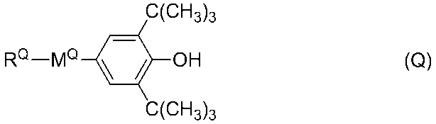
(式中、RQは炭素原子数1から22の直鎖アルキル基又は分岐鎖アルキル基を表し、該アルキル基中の1つ又は2つ以上のCH2基は、酸素原子が直接隣接しないように、-O-、-CH=CH-、-CO-、-OCO-、-COO-、-C≡C-、-CF2O-、-OCF2-で置換されてよく、MQはトランス-1,4-シクロへキシレン基、1,4-フェニレン基又は単結合を表す。)
RQは炭素原子数1から22の直鎖アルキル基又は分岐鎖アルキル基を表し、該アルキル基中の1つ又は2つ以上のCH2基は、酸素原子が直接隣接しないように、-O-、-CH=CH-、-CO-、-OCO-、-COO-、-C≡C-、-CF2O-、-OCF2-で置換されてよいが、炭素原子数1から10の直鎖アルキル基、直鎖アルコキシ基、1つのCH2基が-OCO-又は-COO-に置換された直鎖アルキル基、分岐鎖アルキル基、分岐アルコキシ基、1つのCH2基が-OCO-又は-COO-に置換された分岐鎖アルキル基が好ましく、炭素原子数1から20の直鎖アルキル基、1つのCH2基が-OCO-又は-COO-に置換された直鎖アルキル基、分岐鎖アルキル基、分岐アルコキシ基、1つのCH2基が-OCO-又は-COO-に置換された分岐鎖アルキル基が更に好ましい。MQはトランス-1,4-シクロへキシレン基、1,4-フェニレン基又は単結合を表すが、トランス-1,4-シクロへキシレン基又は1,4-フェニレン基が好ましい。
RQは炭素原子数1から22の直鎖アルキル基又は分岐鎖アルキル基を表し、該アルキル基中の1つ又は2つ以上のCH2基は、酸素原子が直接隣接しないように、-O-、-CH=CH-、-CO-、-OCO-、-COO-、-C≡C-、-CF2O-、-OCF2-で置換されてよいが、炭素原子数1から10の直鎖アルキル基、直鎖アルコキシ基、1つのCH2基が-OCO-又は-COO-に置換された直鎖アルキル基、分岐鎖アルキル基、分岐アルコキシ基、1つのCH2基が-OCO-又は-COO-に置換された分岐鎖アルキル基が好ましく、炭素原子数1から20の直鎖アルキル基、1つのCH2基が-OCO-又は-COO-に置換された直鎖アルキル基、分岐鎖アルキル基、分岐アルコキシ基、1つのCH2基が-OCO-又は-COO-に置換された分岐鎖アルキル基が更に好ましい。MQはトランス-1,4-シクロへキシレン基、1,4-フェニレン基又は単結合を表すが、トランス-1,4-シクロへキシレン基又は1,4-フェニレン基が好ましい。
一般式(Q)で表される化合物は、より具体的には、下記の一般式(Q-a)から一般式(Q-d)で表される化合物が好ましい。

式中、RQ1は炭素原子数1から10の直鎖アルキル基又は分岐鎖アルキル基が好ましく、RQ2は炭素原子数1から20の直鎖アルキル基又は分岐鎖アルキル基が好ましく、RQ3は炭素原子数1から8の直鎖アルキル基、分岐鎖アルキル基、直鎖アルコキシ基又は分岐鎖アルコキシ基が好ましく、LQは炭素原子数1から8の直鎖アルキレン基又は分岐鎖アルキレン基が好ましい。一般式(Q-a)から一般式(Q-d)で表される化合物中、一般式(Q-c)及び一般式(Q-d)で表される化合物が更に好ましい。
本願発明の組成物において、一般式(Q)で表される化合物を1種又は2種を含有することが好ましく、1種から5種含有することが更に好ましく、その含有量は0.001から1%であることが好ましく、0.001から0.1%が更に好ましく、0.001から0.05%が特に好ましい。
本発明の重合性化合物を含有した組成物は、これに含まれる重合性化合物が紫外線照射により重合することで液晶配向能が付与され、組成物の複屈折を利用して光の透過光量を制御する液晶表示素子に使用される。
(液晶表示素子)
本発明の液晶組成物は、以下の構成のIPSモードの液晶表示素子に適用される。図1~6を参照にして、本発明に係るIPSモードの液晶表示素子の例を説明する。
(液晶表示素子)
本発明の液晶組成物は、以下の構成のIPSモードの液晶表示素子に適用される。図1~6を参照にして、本発明に係るIPSモードの液晶表示素子の例を説明する。
図1は、液晶表示素子の構成を模式的に示す図である。図1では、説明のために便宜上各構成要素を離間して記載している。本発明に係る液晶表示素子10の構成は、図1に記載するように、対向に配置された第一基板2と、第二基板7との間に挟持された液晶層5を有するIPSモードの液晶表示素子であって、液晶層5は前述した本発明の液晶組成物により構成される。
第一基板2は、液晶層5側の面に電極層3が形成されている。また、液晶層5と、第一基板2及び第二基板7のそれぞれの間に、液晶層5を構成する液晶組成物と直接当接してホモジニアス配向を誘起する一対の配向膜4を有し、該液晶組成物中の液晶分子は、電圧無印加時に前記第一基板2及び第二基板7に対して略平行になるように配向されている。図1及び図3に示すように、第一基板2および第二基板7は、一対の偏光板1,8により挟持されてもよい。さらに、図1に示すように、第二基板7と配向膜4との間にカラーフィルタ6が設けられていてもよい。
すなわち、本発明に係る液晶表示素子10は、第一偏光板1と、第一基板2と、電極層3と、配向膜4と、液晶組成物を含む液晶層5と、配向膜4と、カラーフィルタ6と、第二基板7と、第二偏光板8と、が順次積層された構成である。第一基板2と第二基板7はガラス又はプラスチックの如き柔軟性をもつ材料を用いることができ、少なくとも一方は透明な材料であり、他方は透明な材料であっても、金属やシリコン等の不透明な材料でも良い。2枚の基板は、周辺領域に配置されたエポキシ系熱硬化性組成物等のシール材及び封止材によって貼り合わされていて、その間には基板間距離を保持するために、例えば、ガラス粒子、プラスチック粒子、アルミナ粒子等の粒状スペーサーまたはフォトリソグラフィー法により形成された樹脂からなるスペーサー柱が配置されていてもよい。
第1電極及び第2電極は透過率を向上させるため透明電極であることが好ましい。透明電極は酸化物半導体(ZnO、InGaZnO、SiGe、GaAs、IZO(Indium Zinc Oxide)、ITO(Indium Tin Oxide)、SnO、TiO、AZTO(AlZnSnO))をスパッタリング等することにより得ることができる。この際、透明電極の、膜厚は10~200nmとすることができる。また、焼成により、アモルファスのITO膜を多結晶のITO膜として、電気的抵抗を低減することもできる。
図2は、図1における第一基板2上に形成された電極層3のII線で囲まれた領域の一部を拡大した平面図である。図2に示すように、第一基板2の表面に形成されている薄膜トランジスタを含む電極層3は、走査信号を供給するための複数のゲートバスライン24と表示信号を供給するための複数のデータバスライン25とが、互いに交差してマトリクス状に配置されている。なお、図2には、一対のゲートバスライン24及び一対のデータバスライン25のみが示されている。
複数のゲートバスライン24と複数のデータバスライン25とにより囲まれた領域により、液晶表示装置の単位画素が形成され、該単位画素内には、第一電極21及び第二電極22が形成されている。ゲートバスライン24とデータバスライン25が互いに交差している交差部近傍には、ソース電極27、ドレイン電極26およびゲート電極28を含む薄膜トランジスタが設けられている。この薄膜トランジスタは、第一電極21に表示信号を供給するスイッチ素子として、第一電極21と連結している。また、ゲートバスライン24と並行して、共通ライン23が設けられる。この共通ライン23は、第二電極22に共通信号を供給するために、第二電極22と連結している。ゲートバスライン24やデータバスライン25、共通ライン23は金属膜であることが好ましく、Al、Cu、Au、Ag、Cr、Ta、Ti、Mo、W、Ni又はその合金がより好ましく、Mo、Al又はその合金の配線を用いる場合が特に好ましい。
図3は、図2におけるIII-III線方向に図1に示す液晶表示素子を切断した断面図である。第一基板2上には、ゲートバスライン24を覆い、且つ第一基板2の略全面を覆うように設けられたゲート絶縁層32と、ゲート絶縁層32の表面に形成された絶縁保護層31とが設けられ、絶縁保護膜31上に、ライン状の第一電極21及びライン状の第二電極22が離間して設けられる。絶縁保護層31は、絶縁機能を有する層であり、窒化ケイ素、二酸化ケイ素、ケイ素酸窒化膜等で形成される。
カラーフィルタ6は、光の漏れを防止する観点で、ブラックマトリクスを形成することが好ましく、薄膜トランジスタに対応する部分にブラックマトリクス(図示せず)を形成することが好ましい。
ブラックマトリクスはアレイ基板と反対側の基板にカラーフィルタと共に設置してもよく、アレイ基板側にカラーフィルタと共に設置してもよく、ブラックマトリクスをアレイ基板、カラーフィルタをもう一方の基板に別に設置しても良い。また、ブラックマトリクスはカラーフィルタと別に設置しても良いが、カラーフィルタの各色を重ねることで透過率を低下させる物であっても良い。
電極層3、及びカラーフィルタ6上には、液晶層5を構成する液晶組成物と直接当接してホモジニアス配向を誘起する一対の配向膜4が設けられている。配向膜4は、例えば、ラビング処理されたポリイミド膜で構成される。
偏光板1及び偏光板8は、各偏光板の偏光軸を調整して視野角やコントラストが良好になるように調整することができ、それらの透過軸がノーマリブラックモードで作動するように、互いに直行する透過軸を有することが好ましい。特に、偏光板1及び偏光板8のうちいずれかは、電圧無印加時の液晶分子の配向方向と平行な透過軸を有するように配置することが好ましい。また、コントラストが最大になるように液晶組成物の屈折率異方性Δnはセル厚dにあわせ調整することが好ましい。更に、視野角を広げるための位相差フィルムも使用することもできる。
図2及び図3に示す実施の形態では、第一電極21及び第二電極22は、絶縁保護層31上に、すなわち同一の層上に形成された櫛形の電極であり、互いに離間して噛合した状態で設けられている。ここで、第一電極21と第二電極22との間の電極間距離:Gと、第一基板2と第二の基板7とに挟持された液晶層の厚さ:Hは、G≧Hの関係を満たす。電極間距離:Gとは、第一電極21と第二電極22との間の、基板に水平方向の最短距離を表し、図2及び図3で示す例においては、第一電極21と第二電極22が噛合して交互に形成されたラインに対して、垂直方向の距離を表す。第一基板2と第二の基板7とに挟持された液晶層の厚さ:Hとは、第一基板2と第二基板7との最表面間の最短距離を表し、具体的には、第一基板2及び第二基板7のそれぞれに設けられた配向膜4(最表面)間の距離(すなわちセルギャップ)のことで、図3に示すように液晶層の厚みを表す。
本発明では、第一電極と第二電極との間の電極間距離:Gと前記第一基板と第二基板とに挟持された液晶層の厚さ:Hとの差が、0≦G-H≦0.5μmの関係を満たすことが好ましい。弾性定数の大きい液晶組成物を用いるとより大きな駆動電圧が必要となるが、上記関係を満たすことにより、駆動電圧を低下させることができる。本発明では、弾性定数の大きい液晶組成物を用いているが、本発明の液晶組成物を用い、且つ0≦G-H≦0.5μmの関係を満たすことで、駆動電圧を低下させると共に、応答速度をより向上させることができる。G-Hは、0より大きいことが好ましく、0.5以下であることが好ましく、0.4以下であることが好ましく、0.3以下であることが好ましく、0.2以下であることが好ましく、0.15以下であることが好ましく、0.1以下であることが好ましい。
IPS型の液晶表示素子は、第一電極21及び第二電極間に形成される基板面に対して水平方向の電界を利用して液晶分子を駆動させる。第一電極21の電極幅:Q、及び第二電極22の電極幅:Rは、発生する電界により液晶層5内の液晶分子が全て駆動され得る程度の幅に形成することが好ましい。具体的には、第一電極及び第二電極の少なくともいずれか一方の電極幅:Wを、透過率の観点から3μm以下とすることが好ましく、2.8μm以下とすることが好ましく、2.6μm以下とすることが好ましく、2.4μm以下とすることが好ましく、2.2μm以下とすることが好ましく、2.0μm以下とすることが好ましく、1.8μm以下とすることが好ましく、1.6μm以下とすることが好ましく、1.4μm以下とすることが好ましく、1.2μm以下とすることが好ましい。しかし、電極幅を狭くすると作成が困難になり、表示素子の歩留まり低下につながってしまう。このため、実際的には0.5μm以上が好ましく、0.7μm以上が好ましく、0.8μm以上が好ましく、0.9μm以上が好ましく、1.0μm以上が好ましい。なお、電極幅とは、第一電極21と第二電極22が噛合して交互に形成されたラインの短軸方向の幅(ライン幅)を表す。
本発明では、前記第一電極と第二電極との間の電極間距離:Gと、前記第一電極及び第二電極の少なくともいずれか一方の電極幅:Wが、G-W≦3μmの関係を満たすことが好ましい。第一電極及び第二電極の少なくともいずれか一方の電極幅:Wとは、第一電極21の電極幅:Qであっても、第二電極22の電極幅:Rであってもよいが、Q及びRの両方の電極幅が等しく、W=Q=Rの関係を満たすことが好ましい。本発明の液晶組成物を用い、且つG-W≦3μmとすることにより、駆動電圧をより低下させると共に、応答速度をより向上させることができる。駆動電圧の低減の観点および透過率の低下を防ぐ観点から、G-Wの下限値は0以上であることが好ましく、0.1以上であることが好ましく、0.1以上であることが好ましく、0.2以上であることが好ましく、0.3以上であることが好ましく、0.5以上であることが好ましい。また、上限値は2.8以下であることが好ましく、2.5以下であることが好ましく、2.3以下であることが好ましく、2.0以下であることが好ましく、1.5以下であることが好ましく、1・3以下であることが好ましく、1.2以下であることが好ましく、1.1以下であることが好ましい。
本発明では、0≦G-H≦0.5μmの関係を満たすか、若しくは、G-W≦3μmの関係を満たすことが好ましいが、0≦G-H≦0.5μmの関係を満たすし、且つG-W≦3μmの関係を満たすことがより好ましい。
図4は、配向膜4により誘起された液晶の配向方向を模式的に示す図である。本発明においては、負の誘電率異方性を有する液晶組成物が用いられる。したがって、第一電極21及び第二電極22の櫛形を形成するラインに対して垂直な方向(水平電界が形成される方向)をx軸としたときに、該x軸と液晶分子30の長軸方向とのなす角θが、概ね0~45°となるように配向されることが好ましい。図4に示す例では、x軸と液晶分子30の長軸方向とのなす角θが、概ね0°の例が示されている。x軸と液晶分子30の長軸方向とのなす角θは、0~40°であることが好ましく、0~35°であることが好ましく、0~30℃であることがより好ましい。このように液晶の配向方向を誘起するのは、液晶表示装置の最大透過率とコントラストを高めるためである。
上記のような構成のIPS型の液晶表示装置10は、薄膜TFTを介して第一電極21に画像信号(電圧)を供給することで、第一電極21と第二電極22との間に電界を生じさせ、この電界によって液晶を駆動する。すなわち、電圧を印加しない状態では、液晶分子30は、その長軸方向が、配向膜4の配向方向と平行になるように配置している。電圧を印加すると、印加した電圧に応じて液晶層5内の液晶分子30は、第一電極21と第二電極22が交互に形成されたラインに対して液晶分子の長軸方向が一定の傾きをもって配向する。なお、図4に示す液晶分子30は、液晶組成物を構成する液晶分子の動きを説明するために模式的に示したものであり、特定の液晶分子のみを意味するものではない。
図1~図4を用いて説明したIPS型の液晶表示素子は一例であって、本発明の技術的思想から逸脱しない限りにおいて、他の様々な形態で実施することが可能である。例えば、図5は、画素内に形成される第一電極21及び第二電極22の他の構成を示す例である。また、図6は、図2におけるIII-III線方向に図1に示す液晶表示素子を切断した他の例である。図6に示すように、第二電極22をゲート絶縁層32上に設け、第二電極を絶縁保護層31で多い、該絶縁保護層31上に第一電極21を設けて、第一電極21及び第二電極22が、異なる層上に設ける構成としてもよい。
本発明の液晶表示素子は、例えば第一基板2上に電極層Al又はその合金等の金属材料をスパッタリングすることにより配線を形成し、電極層3を形成することができる。また、カラーフィルタ6は、例えば、顔料分散法、印刷法、電着法又は、染色法等によって作成することができる。顔料分散法によるカラーフィルタの作成方法を一例に説明すると、カラーフィルタ用の硬化性着色組成物を、該透明基板上に塗布し、パターニング処理を施し、そして加熱又は光照射により硬化させる。この工程を、赤、緑、青の3色についてそれぞれ行うことで、カラーフィルタ用の画素部を作成することができる。また、カラーフィルタはTFT等を有する基板側に設置してもよい。
第一基板2及び第二基板7を、電極層3や配向膜4側が内側となるように対向させるが、その際にスペーサーを介して、基板の間隔を調整してもよい。このときは、液晶層の厚さが1~100μmとなるように調整するのが好ましい。液晶層の厚さは1から20μmが好ましく、1から15μmが好ましく、1から10μmが好ましく、1.3から10μmが好ましく、1.5から10μmが好ましく、1.5から8μmが好ましく、1.5から5μmが好ましく、1.5から4μmが好ましく、1.8から3.5μmが好ましく、2.0から3μmが好ましい。偏光板を使用する場合は、コントラストが最大になるように液晶の屈折率異方性Δnとセル厚dとの積を調整することが好ましい。又、二枚の偏光板がある場合は、各偏光板の偏光軸を調整して視野角やコントラトが良好になるように調整することもできる。更に、視野角を広げるための位相差フィルムも使用することもできる。その後、エポキシ系熱硬化性組成物等のシール剤を、液晶注入口を設けた形で該基板にスクリーン印刷し、該基板同士を貼り合わせ、加熱しシール剤を熱硬化させる。
2枚の基板間に組成物を狭持させる方法は、通常の真空注入法又は滴下注入(ODF:One Drop Fill)法等を用いることができるが、真空注入法においては滴下痕が発生しないものの、注入の跡が残る課題を有しているものであるが、本願発明においては、ODF法を用いて製造する表示素子により好適に使用することができる。ODF法の液晶表示素子製造工程においては、バックプレーン又はフロントプレーンのどちらか一方の基板にエポキシ系光熱併用硬化性などのシール剤を、ディスペンサーを用いて閉ループ土手状に描画し、その中に脱気下で所定量の組成物を滴下後、フロントプレーンとバックプレーンを接合することによって液晶表示素子を製造することができる。本発明においては、ODF法において、液晶組成物を基板に滴下した際の滴下痕の発生を抑えることができる。なお、滴下痕とは、黒表示した場合に液晶組成物を滴下した痕が白く浮かび上がる現象と定義する。
滴下痕の発生は、注入される液晶材料に大きな影響を受けるものであるが、さらに、表示素子の構成によってもその影響は避けられない。IPSモードの液晶表示素子においては、表示素子中に形成される薄膜トランジスタ、及び、櫛形やスリットを有する第一電極21、第二電極22等は、薄い配向膜4、あるいは薄い配向膜4と薄い絶縁保護層31等しか液晶組成物を隔てる部材が無いことから、イオン性物質を遮断しきれない可能性が高く、電極を構成する金属材料と液晶組成物の相互作用による滴下痕の発生を避けることができなかったが、IPS型の液晶表示素子において本願発明の液晶組成物を組み合わせて用いることにより、効果的に滴下痕の発生が抑えられる。
また、ODF法による液晶表示素子の製造工程においては、液晶表示素子のサイズに応じて最適な液晶注入量を滴下する必要があるが、本願発明の液晶組成物は、例えば、液晶滴下時に生じる滴下装置内の急激な圧力変化や衝撃に対する影響が少なく、長時間にわたって安定的に液晶を滴下し続けることが可能であるため、液晶表示素子の歩留まりを高く保持することもできる。特に、最近流行しているスマートフォンに多用される小型液晶表示素子は、最適な液晶注入量が少ないために最適値からのずれを一定範囲内に制御すること自体が難しいが、本願発明の液晶組成物を用いることにより、小型液晶表示素子においても安定した液晶材料の吐出量を実現できる。
本発明の液晶組成物が重合性化合物を含有する場合、重合性化合物を重合させる方法としては、液晶の良好な配向性能を得るためには、適度な重合速度が望ましいので、紫外線又は電子線等の活性エネルギー線を単一又は併用又は順番に照射することによって重合させる方法が好ましい。紫外線を使用する場合、偏光光源を用いても良いし、非偏光光源を用いても良い。また、重合性化合物含有組成物を2枚の基板間に挟持させて状態で重合を行う場合には、少なくとも照射面側の基板は活性エネルギー線に対して適当な透明性が与えられていなければならない。また、光照射時にマスクを用いて特定の部分のみを重合させた後、電場や磁場又は温度等の条件を変化させることにより、未重合部分の配向状態を変化させて、更に活性エネルギー線を照射して重合させるという手段を用いても良い。特に紫外線露光する際には、重合性化合物含有組成物に交流電界を印加しながら紫外線露光することが好ましい。印加する交流電界は、周波数10Hzから10kHzの交流が好ましく、周波数60Hzから10kHzがより好ましく、電圧は液晶表示素子の所望のプレチルト角に依存して選ばれる。つまり、印加する電圧により液晶表示素子のプレチルト角を制御することができる。横電界型MVAモードの液晶表示素子においては、配向安定性及びコントラストの観点からプレチルト角を80度から89.9度に制御することが好ましい。
照射時の温度は、本発明の組成物の液晶状態が保持される温度範囲内であることが好ましい。室温に近い温度、即ち、典型的には15~35℃での温度で重合させることが好ましい。紫外線を発生させるランプとしては、メタルハライドランプ、高圧水銀ランプ、超高圧水銀ランプ等を用いることができる。また、照射する紫外線の波長としては、組成物の吸収波長域でない波長領域の紫外線を照射することが好ましく、必要に応じて、紫外線をカットして使用することが好ましい。照射する紫外線の強度は、0.1mW/cm2~100W/cm2が好ましく、2mW/cm2~50W/cm2がより好ましい。照射する紫外線のエネルギー量は、適宜調整することができるが、10mJ/cm2から500J/cm2が好ましく、100mJ/cm2から200J/cm2がより好ましい。紫外線を照射する際に、強度を変化させても良い。紫外線を照射する時間は照射する紫外線強度により適宜選択されるが、10秒から3600秒が好ましく、10秒から600秒がより好ましい。
カラーフィルタは、例えば、顔料分散法、印刷法、電着法又は、染色法等によって作成することができる。顔料分散法によるカラーフィルタの作成方法を一例に説明すると、カラーフィルタ用の硬化性着色組成物を、該透明基板上に塗布し、パターニング処理を施し、そして加熱又は光照射により硬化させる。この工程を、赤、緑、青の3色についてそれぞれ行うことで、カラーフィルタ用の画素部を作成することができる。その他、該基板上に、TFT、薄膜ダイオード、金属絶縁体金属比抵抗素子等の能動素子を設けた画素電極を設置してもよい。
前記基板を、透明電極層が内側となるように対向させる。その際、スペーサーを介して、基板の間隔を調整してもよい。このときは、得られる調光層の厚さが1~100μmとなるように調整するのが好ましい。1.5から10μmが更に好ましく、偏光板を使用する場合は、コントラストが最大になるように液晶の屈折率異方性Δnとセル厚dとの積を調整することが好ましい。又、二枚の偏光板がある場合は、各偏光板の偏光軸を調整して視野角やコントラトが良好になるように調整することもできる。更に、視野角を広げるための位相差フィルムも使用することもできる。スペーサーとしては、例えば、ガラス粒子、プラスチック粒子、アルミナ粒子、フォトレジスト材料などからなる柱状スペーサー等が挙げられる。その後、エポキシ系熱硬化性組成物等のシール剤を、液晶注入口を設けた形で該基板にスクリーン印刷し、該基板同士を貼り合わせ、加熱しシール剤を熱硬化させる。
2枚の基板間に重合性化合物含有組成物を狭持させる方法は、通常の真空注入法又はODF法などを用いることができるが、真空注入法においては滴下痕が発生しないものの、注入の跡が残る課題を有しているものであるが、本願発明においては、ODF法を用いて製造する表示素子により好適に使用することができる。ODF法の液晶表示素子製造工程においては、バックプレーン又はフロントプレーンのどちらか一方の基板にエポキシ系光熱併用硬化性などのシール剤を、ディスペンサーを用いて閉ループ土手状に描画し、その中に脱気下で所定量の組成物を滴下後、フロントプレーンとバックプレーンを接合することによって液晶表示素子を製造することができる。本発明の組成物は、ODF工程における組成物の滴下が安定的に行えるため、好適に使用することができる。
重合性化合物を重合させる方法としては、液晶の良好な配向性能を得るためには、適度な重合速度が望ましいので、紫外線又は電子線等の活性エネルギー線を単一又は併用又は順番に照射することによって重合させる方法が好ましい。紫外線を使用する場合、偏光光源を用いても良いし、非偏光光源を用いても良い。また、重合性化合物含有組成物を2枚の基板間に挟持させて状態で重合を行う場合には、少なくとも照射面側の基板は活性エネルギー線に対して適当な透明性が与えられていなければならない。また、光照射時にマスクを用いて特定の部分のみを重合させた後、電場や磁場又は温度等の条件を変化させることにより、未重合部分の配向状態を変化させて、更に活性エネルギー線を照射して重合させるという手段を用いても良い。特に紫外線露光する際には、重合性化合物含有組成物に交流電界を印加しながら紫外線露光することが好ましい。印加する交流電界は、周波数10Hzから10kHzの交流が好ましく、周波数60Hzから10kHzがより好ましく、電圧は液晶表示素子の所望のプレチルト角に依存して選ばれる。つまり、印加する電圧により液晶表示素子のプレチルト角を制御することができる。横電界型MVAモードの液晶表示素子においては、配向安定性及びコントラストの観点からプレチルト角を80度から89.9度に制御することが好ましい。
照射時の温度は、本発明の組成物の液晶状態が保持される温度範囲内であることが好ましい。室温に近い温度、即ち、典型的には15~35℃での温度で重合させることが好ましい。紫外線を発生させるランプとしては、メタルハライドランプ、高圧水銀ランプ、超高圧水銀ランプ等を用いることができる。また、照射する紫外線の波長としては、組成物の吸収波長域でない波長領域の紫外線を照射することが好ましく、必要に応じて、紫外線をカットして使用することが好ましい。照射する紫外線の強度は、0.1mW/cm2~100W/cm2が好ましく、2mW/cm2~50W/cm2がより好ましい。照射する紫外線のエネルギー量は、適宜調整することができるが、10mJ/cm2から500J/cm2が好ましく、100mJ/cm2から200J/cm2がより好ましい。紫外線を照射する際に、強度を変化させても良い。紫外線を照射する時間は照射する紫外線強度により適宜選択されるが、10秒から3600秒が好ましく、10秒から600秒がより好ましい。
また、液晶表示素子は、第一の基板2と第二の基板7との間に液晶層5を注入する際、例えば、真空注入法又は滴下注入(ODF:One Drop Fill)法等の方法が行われるが、本願発明においては、ODF法において、液晶組成物を基板に滴下した際の滴下痕の発生を抑えることができる。なお、滴下痕とは、黒表示した場合に液晶組成物を滴下した痕が白く浮かび上がる現象と定義する。
滴下痕の発生は、注入される液晶材料に大きな影響を受けるものであるが、さらに、表示素子の構成によってもその影響は避けられない。本発明の液晶表示素子においては、表示素子中に形成される薄膜トランジスタ、及び、櫛形やスリットを有する画素電極21等は、薄い配向膜4、あるいは薄い配向膜4と薄い絶縁保護層18等しか液晶組成物を隔てる部材が無いことから、イオン性物質を遮断しきれない可能性が高く、電極を構成する金属材料と液晶組成物の相互作用による滴下痕の発生を避けることができなかったが、本発明の液晶表示素子において本願発明の液晶組成物を組み合わせて用いることにより、効果的に滴下痕の発生が抑えられる。
また、ODF法による液晶表示素子の製造工程においては、液晶表示素子のサイズに応じて最適な液晶注入量を滴下する必要があるが、本願発明の液晶組成物は、例えば、液晶滴下時に生じる滴下装置内の急激な圧力変化や衝撃に対する影響が少なく、長時間にわたって安定的に液晶を滴下し続けることが可能であるため、液晶表示素子の歩留まりを高く保持することもできる。特に、最近流行しているスマートフォンに多用される小型液晶表示素子は、最適な液晶注入量が少ないために最適値からのずれを一定範囲内に制御すること自体が難しいが、本願発明の液晶組成物を用いることにより、小型液晶表示素子においても安定した液晶材料の吐出量を実現できる。
実施例において化合物の記載について以下の略号を用いる。なお、nは自然数を表す。
(側鎖)
-n -CnH2n+1 炭素原子数nの直鎖状のアルキル基
n- CnH2n+1- 炭素原子数nの直鎖状のアルキル基
-On -OCnH2n+1 炭素原子数nの直鎖状のアルコキシル基
nO- CnH2n+1O- 炭素原子数nの直鎖状のアルコキシル基
-V -CH=CH2
V- CH2=CH-
-V1 -CH=CH-CH3
1V- CH3-CH=CH-
-2V -CH2-CH2-CH=CH2
V2- CH2=CH-CH2-CH2-
-2V1 -CH2-CH2-CH=CH-CH3
1V2- CH3-CH=CH-CH2-CH2-
(連結基)
-n- -CnH2n-
-nO- -CnH2n-O-
-On- -O-CnH2n-
-COO- -C(=O)-O-
-OCO- -O-C(=O)-
-CF2O- -CF2-O-
-OCF2- -O-CF2-
-CH=CH- -CH=CH-
(環構造)
(側鎖)
-n -CnH2n+1 炭素原子数nの直鎖状のアルキル基
n- CnH2n+1- 炭素原子数nの直鎖状のアルキル基
-On -OCnH2n+1 炭素原子数nの直鎖状のアルコキシル基
nO- CnH2n+1O- 炭素原子数nの直鎖状のアルコキシル基
-V -CH=CH2
V- CH2=CH-
-V1 -CH=CH-CH3
1V- CH3-CH=CH-
-2V -CH2-CH2-CH=CH2
V2- CH2=CH-CH2-CH2-
-2V1 -CH2-CH2-CH=CH-CH3
1V2- CH3-CH=CH-CH2-CH2-
(連結基)
-n- -CnH2n-
-nO- -CnH2n-O-
-On- -O-CnH2n-
-COO- -C(=O)-O-
-OCO- -O-C(=O)-
-CF2O- -CF2-O-
-OCF2- -O-CF2-
-CH=CH- -CH=CH-
(環構造)

実施例中、測定した特性は以下の通りである。
Tni :ネマチック相-等方性液体相転移温度(℃)
T→N :ネマチック相下限温度(℃)
Δn :20℃における屈折率異方性
Δε :20℃における誘電率異方性
γ1 :20℃における回転粘度(mPa・s)
K33 :20℃における弾性定数K33(pN)
応答速度 : VA型の液晶表示素子の20℃における応答速度を、オートロニック社製電気光学測定装置DMS703により測定した。
VHR(UV):高圧水銀ランプを用いて、365nmにおける照度が100mW/cm2の光を120秒照射した後の、周波数60Hz、印加電圧1V、60℃における電圧保持率(%)
焼き付き : 液晶表示素子の焼き付き評価は、表示エリア内に所定の固定パターンを任意の試験時間表示させた後に、全画面均一な表示を行ったときの固定パターンの残像が、許容できない残像レベルに達するまでの試験時間を計測した。
1)ここで言う試験時間とは固定パターンの表示時間を示し、この時間が長いほど残像の発生が抑制されており、性能が高いことを示している。
2)許容できない残像レベルとは、出荷合否判定で不合格となる残像が観察されるレベルである。
例)
サンプルA:1000時間
サンプルB:500時間
サンプルC:200時間
サンプルD:100時間
性能は、A>B>C>Dである。
T→N :ネマチック相下限温度(℃)
Δn :20℃における屈折率異方性
Δε :20℃における誘電率異方性
γ1 :20℃における回転粘度(mPa・s)
K33 :20℃における弾性定数K33(pN)
応答速度 : VA型の液晶表示素子の20℃における応答速度を、オートロニック社製電気光学測定装置DMS703により測定した。
VHR(UV):高圧水銀ランプを用いて、365nmにおける照度が100mW/cm2の光を120秒照射した後の、周波数60Hz、印加電圧1V、60℃における電圧保持率(%)
焼き付き : 液晶表示素子の焼き付き評価は、表示エリア内に所定の固定パターンを任意の試験時間表示させた後に、全画面均一な表示を行ったときの固定パターンの残像が、許容できない残像レベルに達するまでの試験時間を計測した。
1)ここで言う試験時間とは固定パターンの表示時間を示し、この時間が長いほど残像の発生が抑制されており、性能が高いことを示している。
2)許容できない残像レベルとは、出荷合否判定で不合格となる残像が観察されるレベルである。
例)
サンプルA:1000時間
サンプルB:500時間
サンプルC:200時間
サンプルD:100時間
性能は、A>B>C>Dである。
滴下痕 :
液晶表示装置の滴下痕の評価は、全面黒表示した場合における白く浮かび上がる滴下痕を目視にて以下の5段階評価で行った。
液晶表示装置の滴下痕の評価は、全面黒表示した場合における白く浮かび上がる滴下痕を目視にて以下の5段階評価で行った。
5:滴下痕無し(優)
4:滴下痕ごく僅かに有るも許容できるレベル(良)
3:滴下痕僅かに有り、合否判定のボーダーラインレベル(条件付で可)
2:滴下痕有り許容できないレベル(不可)
1:滴下痕有りかなり劣悪(悪)
低温でのネマチック相安定性 :
低温でのネマチック相安定性の評価は、組成物を調製後、2mLのサンプル瓶に組成物を1g秤量し、これに温度制御式試験槽の中で、次の運転状態「-20℃(1時間保持)→昇温(0.1℃/毎分)→0℃(1時間保持)→昇温(0.1℃/毎分)→20℃(1時間保持)→降温(-0.1℃/毎分)→0℃(1時間保持)→降温(-0.1℃/毎分)→-20℃」を1サイクルとして温度変化を与え続け、目視にて組成物からの析出物の発生を観察し、析出物が観察されたときの試験時間を計測した。
試験時間が長いほど長時間にわたって安定して液晶相を保っており、低温でのネマチック相安定性が良好である。
例)
サンプルA:24時間
サンプルB:120時間
サンプルC:48時間
サンプルD:240時間
性能は、D>B>C>Aである。
4:滴下痕ごく僅かに有るも許容できるレベル(良)
3:滴下痕僅かに有り、合否判定のボーダーラインレベル(条件付で可)
2:滴下痕有り許容できないレベル(不可)
1:滴下痕有りかなり劣悪(悪)
低温でのネマチック相安定性 :
低温でのネマチック相安定性の評価は、組成物を調製後、2mLのサンプル瓶に組成物を1g秤量し、これに温度制御式試験槽の中で、次の運転状態「-20℃(1時間保持)→昇温(0.1℃/毎分)→0℃(1時間保持)→昇温(0.1℃/毎分)→20℃(1時間保持)→降温(-0.1℃/毎分)→0℃(1時間保持)→降温(-0.1℃/毎分)→-20℃」を1サイクルとして温度変化を与え続け、目視にて組成物からの析出物の発生を観察し、析出物が観察されたときの試験時間を計測した。
試験時間が長いほど長時間にわたって安定して液晶相を保っており、低温でのネマチック相安定性が良好である。
例)
サンプルA:24時間
サンプルB:120時間
サンプルC:48時間
サンプルD:240時間
性能は、D>B>C>Aである。
揮発性/製造装置汚染性 :
液晶材料の揮発性評価は、液晶組成物0.020gを1Paの環境下に90分放置したときの質量変化を評価した。
質量変化が小さいほど揮発しにくく、製造装置を汚染しないので、高性能であることを示す。
例)
サンプルA:0.019g
サンプルB:0.017g
サンプルC:0.018g
サンプルD:0.013g
性能は、A>C>B>Dである。
(実施例1、比較例1、比較例2及び実施例2)
実施例1、比較例1、比較例2及び実施例2の液晶組成物を調製し、これらの物性値を測定した結果を下表に示す。
液晶材料の揮発性評価は、液晶組成物0.020gを1Paの環境下に90分放置したときの質量変化を評価した。
質量変化が小さいほど揮発しにくく、製造装置を汚染しないので、高性能であることを示す。
例)
サンプルA:0.019g
サンプルB:0.017g
サンプルC:0.018g
サンプルD:0.013g
性能は、A>C>B>Dである。
(実施例1、比較例1、比較例2及び実施例2)
実施例1、比較例1、比較例2及び実施例2の液晶組成物を調製し、これらの物性値を測定した結果を下表に示す。

実施例1として示した組成物は、本願請求項1に記載した一般式(i)で表される化合物、一般式(ii)で表される化合物、一般式(iii)で表される化合物、一般式(iv)で表される化合物、一般式(v)で表される化合物及び一般式(vi)で表される化合物を含有し、かつそれらの含有量が96%である組成物である。
これに対し、比較例1として示した組成物は、実施例1に対して一般式(iii)で表される化合物及び一般式(iv)で表される化合物の含有量を減少させ、3-CyCy-1及びV2-PhPh-1を添加し、組成物中の一般式(i)で表される化合物、一般式(ii)で表される化合物、一般式(iii)で表される化合物、一般式(iv)で表される化合物、一般式(v)で表される化合物及び一般式(vi)で表される化合物の合計の含有量が85%とした組成物である。
更に比較例2として示した組成物は、実施例1に対して一般式(ii)で表される化合物及び一般式(iii)で表される化合物の含有量を減少させ、3-Cy-1O-PH5-O2及び3-Cy-CH=CH-Cy-2を添加し、組成物中の一般式(i)で表される化合物、一般式(ii)で表される化合物、一般式(iii)で表される化合物、一般式(iv)で表される化合物、一般式(v)で表される化合物及び一般式(vi)で表される化合物の合計の含有量が79%とした組成物である。
更に実施例1、比較例1、比較例2及び実施例2の組成物の評価結果を下表に示す。

実施例1の組成物に対し、比較例1の組成物はγ1の値こそ改善するものの、Tniは低下しており、焼き付き及び滴下痕の悪化が顕著であった。揮発性も悪化していた。
比較例2の組成物はγ1の値こそ改善するものの、Tniは大きく低下しており、焼き付き、滴下痕及び低温でのネマチック相安定性が顕著に悪化していた。
実施例1の組成物は、所望のTni、Δε、γ1、低温でのネマチック相安定性等の諸特性が得られ、焼き付き、滴下痕、低温でのネマチック安定性、揮発性が優れたものであり、セル厚3.2μmのVA方式の液晶表示素子を作製し、応答速度を評価し、十分に高速応答であることを確認した。また、液晶テレビに求められる高透過率が得られることを確認した。
また、実施例1、比較例1、比較例2及び実施例2の組成物を用いたVA型液晶表示素子のVHR(UV)を評価したところ、実施例1及び実施例2は十分に高い数値が得られ、高信頼性であることが確認されたが、比較例1及び比較例2はVHR(UV)の低下が確認された。
また、実施例1、比較例1、比較例2及び実施例2の組成物を用いたVA型液晶表示素子のVHR(UV)を評価したところ、実施例1及び実施例2は十分に高い数値が得られ、高信頼性であることが確認されたが、比較例1及び比較例2はVHR(UV)の低下が確認された。
以上のように本発明の組成物は、Tni、Δε、γ1、低温でのネマチック相安定性等の液晶表示素子としての諸特性及び表示素子の焼き付き特性を悪化させること無く、製造時の滴下痕が発生し難く、ODF工程におけて揮発し難い組成物を提供でき、これを用いた液晶表示素子は高速応答かつ高信頼性であることがわかった。
1,8 偏光板
2 第一基板
3 電極層
4 配向膜
5 液晶層
6 カラーフィルタ
7 第二基板
21 第一電極
22 第二電極
23 共通ライン
24 ゲートバスライン
25 データバスライン
26 ドレイン電極
27 ソース電極
28 ゲート電極
30 液晶分子
31 絶縁保護層
32 ゲート絶縁層
H 前記第一基板と第二基板2枚の基板に挟持された液晶層の厚さ
G 第一電極と第二電極との間の電極間距離
W 第一電極及び第二電極の電極幅
R 第二電極22の電極幅
Q 第一電極21の電極幅
2 第一基板
3 電極層
4 配向膜
5 液晶層
6 カラーフィルタ
7 第二基板
21 第一電極
22 第二電極
23 共通ライン
24 ゲートバスライン
25 データバスライン
26 ドレイン電極
27 ソース電極
28 ゲート電極
30 液晶分子
31 絶縁保護層
32 ゲート絶縁層
H 前記第一基板と第二基板2枚の基板に挟持された液晶層の厚さ
G 第一電極と第二電極との間の電極間距離
W 第一電極及び第二電極の電極幅
R 第二電極22の電極幅
Q 第一電極21の電極幅
Claims (4)
- 一般式(i)で表される化合物、一般式(ii)で表される化合物、一般式(iii)で表される化合物、一般式(iv)で表される化合物、一般式(v)で表される化合物及び一般式(vi)で表される化合物を含有し、組成物中の一般式(i)で表される化合物、一般式(ii)で表される化合物、一般式(iii)で表される化合物、一般式(iv)で表される化合物、一般式(v)で表される化合物及び一般式(vi)で表される化合物の合計の含有量が90%以上である組成物。
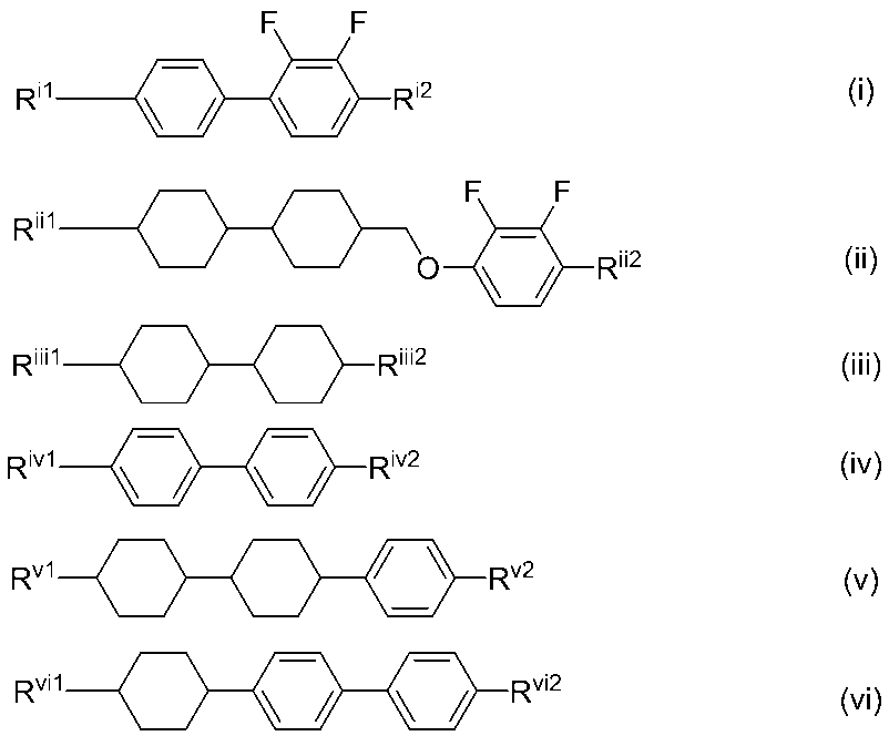
- 更に一般式(L)で表される化合物を含有する請求項1に記載の組成物。

nL1は0、1、2又は3を表し、
AL1、AL2及びAL3はそれぞれ独立して
(a) 1,4-シクロヘキシレン基(この基中に存在する1個の-CH2-又は隣接していない2個以上の-CH2-は-O-に置き換えられてもよい。)及び
(b) 1,4-フェニレン基(この基中に存在する1個の-CH=又は隣接していない2個以上の-CH=は-N=に置き換えられてもよい。)
(c) (c)ナフタレン-2,6-ジイル基、1,2,3,4-テトラヒドロナフタレン-2,6-ジイル基又はデカヒドロナフタレン-2,6-ジイル基(ナフタレン-2,6-ジイル基又は1,2,3,4-テトラヒドロナフタレン-2,6-ジイル基中に存在する1個の-CH=又は隣接していない2個以上の-CH=は-N=に置き換えられても良い。)
からなる群より選ばれる基を表し、上記の基(a)、基(b)及び基(c)はそれぞれ独立して1個のシアノ基、フッ素原子又は塩素原子で置換されていても良く、
ZL1及びZL2はそれぞれ独立して単結合、-CH2CH2-、-(CH2)4-、-OCH2-、-CH2O-、-COO-、-OCO-、-OCF2-、-CF2O-、-CH=N-N=CH-、-CH=CH-、-CF=CF-又は-C≡C-を表し、
nL1が2又は3であってAL2が複数存在する場合は、それらは同一であっても異なっていても良く、nL1が2又は3であってZL3が複数存在する場合は、それらは同一であっても異なっていても良いが、一般式(iii)~(vi)で表される化合物を除く。) - 請求項1又は2記載の組成物を使用した液晶表示素子。
- 請求項1又は2記載の液晶組成物を用いたFFS型又はIPS型の液晶表示素子。
Priority Applications (3)
| Application Number | Priority Date | Filing Date | Title |
|---|---|---|---|
| US16/096,410 US20190119573A1 (en) | 2016-06-10 | 2017-05-25 | Composition and liquid crystal display device |
| CN201780021747.7A CN109072080A (zh) | 2016-06-10 | 2017-05-25 | 组合物及液晶显示元件 |
| JP2017548073A JP6296321B1 (ja) | 2016-06-10 | 2017-05-25 | 組成物及び液晶表示素子 |
Applications Claiming Priority (2)
| Application Number | Priority Date | Filing Date | Title |
|---|---|---|---|
| JP2016-116199 | 2016-06-10 | ||
| JP2016116199 | 2016-06-10 |
Publications (1)
| Publication Number | Publication Date |
|---|---|
| WO2017212933A1 true WO2017212933A1 (ja) | 2017-12-14 |
Family
ID=60577836
Family Applications (1)
| Application Number | Title | Priority Date | Filing Date |
|---|---|---|---|
| PCT/JP2017/019517 Ceased WO2017212933A1 (ja) | 2016-06-10 | 2017-05-25 | 組成物及び液晶表示素子 |
Country Status (4)
| Country | Link |
|---|---|
| US (1) | US20190119573A1 (ja) |
| JP (1) | JP6296321B1 (ja) |
| CN (1) | CN109072080A (ja) |
| WO (1) | WO2017212933A1 (ja) |
Citations (3)
| Publication number | Priority date | Publication date | Assignee | Title |
|---|---|---|---|---|
| WO2014024648A1 (ja) * | 2012-08-08 | 2014-02-13 | Jnc株式会社 | 液晶組成物および液晶表示素子 |
| WO2015060056A1 (ja) * | 2013-10-22 | 2015-04-30 | Jnc株式会社 | 液晶組成物および液晶表示素子 |
| JP2016069384A (ja) * | 2014-09-26 | 2016-05-09 | Jnc株式会社 | 液晶組成物および液晶表示素子 |
Family Cites Families (4)
| Publication number | Priority date | Publication date | Assignee | Title |
|---|---|---|---|---|
| KR101373734B1 (ko) * | 2006-12-11 | 2014-03-14 | 삼성디스플레이 주식회사 | 액정 조성물 및 이를 포함하는 액정 표시 장치 |
| TWI623609B (zh) * | 2013-03-06 | 2018-05-11 | Dainippon Ink & Chemicals | Nematic liquid crystal composition and liquid crystal display element using same |
| CN105793770A (zh) * | 2013-12-11 | 2016-07-20 | Dic株式会社 | 液晶显示元件及其制造方法 |
| JP5888477B2 (ja) * | 2014-02-27 | 2016-03-22 | Dic株式会社 | 液晶表示装置 |
-
2017
- 2017-05-25 JP JP2017548073A patent/JP6296321B1/ja active Active
- 2017-05-25 WO PCT/JP2017/019517 patent/WO2017212933A1/ja not_active Ceased
- 2017-05-25 CN CN201780021747.7A patent/CN109072080A/zh active Pending
- 2017-05-25 US US16/096,410 patent/US20190119573A1/en not_active Abandoned
Patent Citations (3)
| Publication number | Priority date | Publication date | Assignee | Title |
|---|---|---|---|---|
| WO2014024648A1 (ja) * | 2012-08-08 | 2014-02-13 | Jnc株式会社 | 液晶組成物および液晶表示素子 |
| WO2015060056A1 (ja) * | 2013-10-22 | 2015-04-30 | Jnc株式会社 | 液晶組成物および液晶表示素子 |
| JP2016069384A (ja) * | 2014-09-26 | 2016-05-09 | Jnc株式会社 | 液晶組成物および液晶表示素子 |
Also Published As
| Publication number | Publication date |
|---|---|
| CN109072080A (zh) | 2018-12-21 |
| JP6296321B1 (ja) | 2018-03-20 |
| US20190119573A1 (en) | 2019-04-25 |
| JPWO2017212933A1 (ja) | 2018-06-14 |
Similar Documents
| Publication | Publication Date | Title |
|---|---|---|
| WO2017082230A1 (ja) | 組成物及びそれを使用した液晶表示素子 | |
| JPWO2017098954A1 (ja) | 液晶表示素子 | |
| JP6565648B2 (ja) | 液晶表示素子 | |
| WO2014155534A1 (ja) | 液晶組成物及びそれを使用した液晶表示素子 | |
| JP6132122B2 (ja) | 液晶組成物及びこれを用いた液晶表示素子 | |
| US9637684B2 (en) | Composition and liquid crystal display element using same | |
| US20180148647A1 (en) | Composition and liquid crystal display using same | |
| WO2015037519A1 (ja) | 組成物及びそれを使用した液晶表示素子 | |
| WO2016052006A1 (ja) | 組成物及びそれを使用した液晶表示素子 | |
| WO2018043144A1 (ja) | 液晶表示素子 | |
| JP6268562B1 (ja) | 組成物及びそれを使用した液晶表示素子 | |
| WO2017195585A1 (ja) | 液晶表示素子 | |
| JP6409995B2 (ja) | 液晶表示素子 | |
| WO2014155532A1 (ja) | 液晶組成物及びそれを使用した液晶表示素子 | |
| JP6296321B1 (ja) | 組成物及び液晶表示素子 | |
| WO2015037517A1 (ja) | 組成物及びそれを使用した液晶表示素子 | |
| WO2016056314A1 (ja) | 組成物及びそれを使用した液晶表示素子 | |
| WO2015037515A1 (ja) | 組成物及びそれを使用した液晶表示素子 | |
| JP2015074702A (ja) | 組成物及びそれを使用した液晶表示素子 | |
| WO2018207635A1 (ja) | 組成物及びそれを使用した液晶表示素子 | |
| JP7318204B2 (ja) | 液晶組成物及び液晶表示素子 | |
| WO2016056313A1 (ja) | 組成物及びそれを使用した液晶表示素子 | |
| WO2015053018A1 (ja) | 組成物及びそれを使用した液晶表示素子 | |
| WO2016013690A1 (ja) | 液晶組成物及びそれを使用した液晶表示素子 | |
| WO2015053017A1 (ja) | 組成物及びそれを使用した液晶表示素子 |
Legal Events
| Date | Code | Title | Description |
|---|---|---|---|
| ENP | Entry into the national phase |
Ref document number: 2017548073 Country of ref document: JP Kind code of ref document: A |
|
| 121 | Ep: the epo has been informed by wipo that ep was designated in this application |
Ref document number: 17810113 Country of ref document: EP Kind code of ref document: A1 |
|
| NENP | Non-entry into the national phase |
Ref country code: DE |
|
| 122 | Ep: pct application non-entry in european phase |
Ref document number: 17810113 Country of ref document: EP Kind code of ref document: A1 |