WO2017208713A1 - 樹脂多層基板 - Google Patents
樹脂多層基板 Download PDFInfo
- Publication number
- WO2017208713A1 WO2017208713A1 PCT/JP2017/016974 JP2017016974W WO2017208713A1 WO 2017208713 A1 WO2017208713 A1 WO 2017208713A1 JP 2017016974 W JP2017016974 W JP 2017016974W WO 2017208713 A1 WO2017208713 A1 WO 2017208713A1
- Authority
- WO
- WIPO (PCT)
- Prior art keywords
- conductor
- component
- conductor via
- laminate
- multilayer substrate
- Prior art date
- Legal status (The legal status is an assumption and is not a legal conclusion. Google has not performed a legal analysis and makes no representation as to the accuracy of the status listed.)
- Ceased
Links
Images





Classifications
-
- H—ELECTRICITY
- H05—ELECTRIC TECHNIQUES NOT OTHERWISE PROVIDED FOR
- H05K—PRINTED CIRCUITS; CASINGS OR CONSTRUCTIONAL DETAILS OF ELECTRIC APPARATUS; MANUFACTURE OF ASSEMBLAGES OF ELECTRICAL COMPONENTS
- H05K1/00—Printed circuits
- H05K1/02—Details
- H05K1/0213—Electrical arrangements not otherwise provided for
- H05K1/0216—Reduction of cross-talk, noise or electromagnetic interference
- H05K1/0218—Reduction of cross-talk, noise or electromagnetic interference by printed shielding conductors, ground planes or power plane
- H05K1/0219—Printed shielding conductors for shielding around or between signal conductors, e.g. coplanar or coaxial printed shielding conductors
- H05K1/0222—Printed shielding conductors for shielding around or between signal conductors, e.g. coplanar or coaxial printed shielding conductors for shielding around a single via or around a group of vias, e.g. coaxial vias or vias surrounded by a grounded via fence
-
- H—ELECTRICITY
- H05—ELECTRIC TECHNIQUES NOT OTHERWISE PROVIDED FOR
- H05K—PRINTED CIRCUITS; CASINGS OR CONSTRUCTIONAL DETAILS OF ELECTRIC APPARATUS; MANUFACTURE OF ASSEMBLAGES OF ELECTRICAL COMPONENTS
- H05K1/00—Printed circuits
- H05K1/02—Details
- H05K1/0296—Conductive pattern lay-out details not covered by sub groups H05K1/02 - H05K1/0295
- H05K1/0298—Multilayer circuits
-
- H—ELECTRICITY
- H05—ELECTRIC TECHNIQUES NOT OTHERWISE PROVIDED FOR
- H05K—PRINTED CIRCUITS; CASINGS OR CONSTRUCTIONAL DETAILS OF ELECTRIC APPARATUS; MANUFACTURE OF ASSEMBLAGES OF ELECTRICAL COMPONENTS
- H05K1/00—Printed circuits
- H05K1/02—Details
- H05K1/11—Printed elements for providing electric connections to or between printed circuits
- H05K1/115—Via connections; Lands around holes or via connections
-
- H—ELECTRICITY
- H05—ELECTRIC TECHNIQUES NOT OTHERWISE PROVIDED FOR
- H05K—PRINTED CIRCUITS; CASINGS OR CONSTRUCTIONAL DETAILS OF ELECTRIC APPARATUS; MANUFACTURE OF ASSEMBLAGES OF ELECTRICAL COMPONENTS
- H05K3/00—Apparatus or processes for manufacturing printed circuits
- H05K3/46—Manufacturing multilayer circuits
- H05K3/4611—Manufacturing multilayer circuits by laminating two or more circuit boards
- H05K3/4626—Manufacturing multilayer circuits by laminating two or more circuit boards characterised by the insulating layers or materials
- H05K3/4632—Manufacturing multilayer circuits by laminating two or more circuit boards characterised by the insulating layers or materials laminating thermoplastic or uncured resin sheets comprising printed circuits without added adhesive materials between the sheets
-
- H—ELECTRICITY
- H05—ELECTRIC TECHNIQUES NOT OTHERWISE PROVIDED FOR
- H05K—PRINTED CIRCUITS; CASINGS OR CONSTRUCTIONAL DETAILS OF ELECTRIC APPARATUS; MANUFACTURE OF ASSEMBLAGES OF ELECTRICAL COMPONENTS
- H05K1/00—Printed circuits
- H05K1/18—Printed circuits structurally associated with non-printed electric components
- H05K1/182—Printed circuits structurally associated with non-printed electric components associated with components mounted in printed circuit boards [PCB], e.g. insert-mounted components [IMC]
- H05K1/185—Printed circuits structurally associated with non-printed electric components associated with components mounted in printed circuit boards [PCB], e.g. insert-mounted components [IMC] associated with components encapsulated in the insulating substrate of the PCBs; associated with components incorporated in internal layers of multilayer circuit boards
-
- H—ELECTRICITY
- H05—ELECTRIC TECHNIQUES NOT OTHERWISE PROVIDED FOR
- H05K—PRINTED CIRCUITS; CASINGS OR CONSTRUCTIONAL DETAILS OF ELECTRIC APPARATUS; MANUFACTURE OF ASSEMBLAGES OF ELECTRICAL COMPONENTS
- H05K2201/00—Indexing scheme relating to printed circuits covered by H05K1/00
- H05K2201/09—Shape and layout
- H05K2201/09209—Shape and layout details of conductors
- H05K2201/095—Conductive through-holes or vias
- H05K2201/096—Vertically aligned vias, holes or stacked vias
-
- H—ELECTRICITY
- H05—ELECTRIC TECHNIQUES NOT OTHERWISE PROVIDED FOR
- H05K—PRINTED CIRCUITS; CASINGS OR CONSTRUCTIONAL DETAILS OF ELECTRIC APPARATUS; MANUFACTURE OF ASSEMBLAGES OF ELECTRICAL COMPONENTS
- H05K2201/00—Indexing scheme relating to printed circuits covered by H05K1/00
- H05K2201/10—Details of components or other objects attached to or integrated in a printed circuit board
- H05K2201/10613—Details of electrical connections of non-printed components, e.g. special leads
- H05K2201/10621—Components characterised by their electrical contacts
- H05K2201/10636—Leadless chip, e.g. chip capacitor or resistor
-
- Y—GENERAL TAGGING OF NEW TECHNOLOGICAL DEVELOPMENTS; GENERAL TAGGING OF CROSS-SECTIONAL TECHNOLOGIES SPANNING OVER SEVERAL SECTIONS OF THE IPC; TECHNICAL SUBJECTS COVERED BY FORMER USPC CROSS-REFERENCE ART COLLECTIONS [XRACs] AND DIGESTS
- Y02—TECHNOLOGIES OR APPLICATIONS FOR MITIGATION OR ADAPTATION AGAINST CLIMATE CHANGE
- Y02P—CLIMATE CHANGE MITIGATION TECHNOLOGIES IN THE PRODUCTION OR PROCESSING OF GOODS
- Y02P70/00—Climate change mitigation technologies in the production process for final industrial or consumer products
- Y02P70/50—Manufacturing or production processes characterised by the final manufactured product
Definitions
- the present invention relates to a resin multilayer substrate.
- the conductor via and the conductor pattern are electrically connected so as to be alternately connected.
- disconnection between the conductor via and the conductor pattern becomes a problem.
- the serial via part has higher rigidity than other parts (resin layer) in the laminate, the coplanarity of the outermost surface of the laminate deteriorates when pressed to integrate the laminate There is. If the coplanarity of the outermost surface deteriorates, it may become impossible to correctly mount the component when trying to mount the component on the surface later.
- the interval between the built-in parts is set narrow, the shape of the series via portion is distorted during pressurization for the integration of the laminated body, and a short circuit occurs due to contact between the plurality of series via portions. There is a fear.
- the built-in component has higher rigidity than the resin layer in the laminate, a short circuit due to contact between components is also a problem for the same reason.
- the outermost surface of the multilayer body in the portion where the serial via part and the built-in part are arranged when pressed to integrate the multilayer body since the serial via part and the built-in component have high rigidity, the outermost surface of the multilayer body in the portion where the serial via part and the built-in part are arranged when pressed to integrate the multilayer body.
- the coplanarity of may worsen.
- the coplanarity of the outermost surface deteriorates, it may become impossible to correctly mount the component when trying to mount the component on the outermost surface later.
- an object of the present invention is to provide a resin multilayer substrate that can alleviate at least one of these problems.
- a resin multilayer substrate includes a laminate in which a plurality of resin layers mainly composed of a thermoplastic resin are laminated, a built-in laminate, and a first component terminal.
- a first component that is included in the laminate has a second component terminal, and is disposed so as to be separated from the first component when viewed from the stacking direction of the laminate.
- a first conductor via that is electrically connected to one component terminal and overlaps the first component terminal when viewed from the stacking direction of the laminate, and from the first conductor via to the second component side.
- a plurality of second conductor vias which are at a different height from the first conductor vias while being shifted and are electrically connected to the first conductor vias.
- the present invention it is possible to prevent a short circuit due to contact between serial via parts or a short circuit due to contact between parts due to distortion or inclination of the serial via part. As a result of the flexibility of the serial via portion as a whole, disconnection of the serial via portion can be prevented.
- FIG. 4 is a cross-sectional view taken along the line IV-IV in FIG. 3. It is a perspective top view of the resin multilayer substrate in Embodiment 3 based on this invention.
- FIG. 6 is a cross-sectional view taken along the line VI-VI in FIG. 5. It is a perspective top view of the resin multilayer substrate in Embodiment 4 based on this invention.
- FIG. 8 is a cross-sectional view taken along line VIII-VIII in FIG. 7.
- FIG. 10 is a cross-sectional view taken along line XX in FIG. 9. It is a perspective top view of the resin multilayer substrate in Embodiment 6 based on this invention.
- FIG. 12 is a cross-sectional view taken along the line XII-XII in FIG. 11.
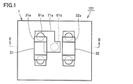
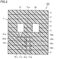
- FIG. 1 shows a cross-sectional view taken along the line II-II in FIG.
- a resin multilayer substrate 101 includes a laminate 1 in which a plurality of resin layers 2 mainly composed of a thermoplastic resin are laminated, and a first component terminal 31a that is built in the laminate 1 and includes a first component terminal 31a.
- a first component 31, a second component 32 that is built in the stacked body 1, has a second component terminal 32 a, and is disposed so as to be separated from the first component 31 when viewed from the stacking direction of the stacked body 1;
- a conductor via 61a as a first conductor via that is electrically connected to the one component terminal 31a and overlaps the first component terminal 31a when viewed from the stacking direction of the multilayer body 1, and a first via from the first conductor via.
- a plurality of conductor vias 61b, 61c, and 61d are provided as second conductor vias that are shifted to the two-component 32 side and are at a different height from the first conductor via and are electrically connected to the first conductor via.
- the first component terminal 31a and the conductor via 61a as the first conductor via are directly connected without a planar conductor pattern therebetween.
- a planar conductor pattern 71a is connected to the lower end of the conductor via 61a, and a conductor via 61b is connected to the lower surface of the conductor pattern 71a. That is, the planar conductor pattern 71a is a lead for connecting the conductor via 61a as the first conductor via and the conductor via 61b as the second conductor via shifted from the first conductor via to the second component 32 side. Functions as a conductor.
- a conductor via 61c is connected to the lower end of the conductor via 61b as the second conductor via via a conductor pattern 71b.
- a conductor via 61d is connected to the lower end of the conductor via 61c via a conductor pattern 71c.
- a conductor pattern 71d is connected to the lower end of the conductor via 61d.
- the conductor vias 61c and 61d also correspond to the second conductor via.
- the conductor patterns 71b, 71c, 71d function as pad conductors for connecting the conductor vias.
- the conductor vias 61b, 61c, 61d as the second conductor vias continue linearly.
- the number of second conductor vias is not limited to 3, and may be 2 or 4 or more.
- the serial via portion having a shape including the conductor via 61a as the first conductor via and the conductor vias 61b, 61c and 61d as the second conductor via is drawn out from the first component 31. Since the conductor vias 61b, 61c, 61d as the conductor vias are shifted to the second component 32 side as compared with the conductor via 61a as the first conductor via, the series via having higher rigidity than the other parts of the multilayer body 1 It can suppress that a part overlaps with the 1st component 31 in the lamination direction. Further, in the present embodiment, a part of the serial via portion is located between the first component 31 and the second component 32 when viewed from the stacking direction.
- the parts (the first part 31 and the second part 32), the serial via part, and the like have higher rigidity than the other parts (resin layer, etc.) of the laminated body 1, and pressurization for integrating the laminated body.
- the pressure applied to the laminated body tends to be unbalanced, but it is possible to balance by arranging a part of a portion having high rigidity between a plurality of parts (the first part 31 and the second part 32). it can.
- the serial via portions from contacting each other when the serial via portions are inclined, or the components from contacting each other when the components are inclined. Therefore, an undesired short circuit can be prevented.
- the degree of deterioration of the coplanarity of the outermost surface of the laminate can be reduced by preventing a part of the series via portion from overlapping when viewed from the lamination direction.
- the series via portions are not continuous only in the thickness direction, but the conductor vias 61b, 61c, 61d as the second conductor vias are compared with the conductor via 61a as the first conductor via in the middle of the series via portion. Therefore, the series via portion has flexibility as a spring as a whole. Since the serial via portion has flexibility as a whole, it is possible to avoid an excessive load on the serial via portion as much as possible, and to avoid a disconnection due to an excessive load as much as possible.
- At least one planar conductor pattern is interposed between the first conductor via and the second conductor via.
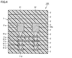
- FIG. 4 shows a cross-sectional view taken along the line IV-IV in FIG.
- the resin multilayer substrate 102 in the present embodiment includes a laminate 1 in which a plurality of resin layers 2 mainly composed of a thermoplastic resin are laminated, and a first component terminal 31a that is built in the laminate 1 and includes a first component terminal 31a.
- the conductor vias 61a, 61c and 61d as the first conductor vias are discontinuous, but are linearly arranged.
- the resin multilayer substrate 102 further includes a third conductor via 62a.
- the third conductor via 62a is electrically connected to the second component terminal 32a and is located at a position overlapping the second component terminal 32a when viewed from the stacking direction of the multilayer body 1.
- the opposite end of the third conductor via 62a connected to the second component terminal 32a is connected to the conductor pattern 72a.
- the resin multilayer substrate 102 has a height different from that of the third conductor via while being shifted from the conductor via 62a serving as the third conductor via to the first component 31 side, and is electrically connected to the third conductor via. It is preferable to further include a conductor via 62b as a via. In this case, it is preferable that a plurality of fourth conductor vias exist. That is, it is preferable that the plurality of conductor vias 62b constitute the series via portion as the fourth conductor via.
- the first component 31 and the serial via portion connected thereto are L-shaped in a plan view.
- the two L-shapes are arranged in combination with each other in a point-symmetric positional relationship.
- the conductor vias 61a, 61c, 61d are overlapped and these conductor vias are also overlapped with the first component 31, so that the pressure tends to be unbalanced as it is.
- the pressure can be balanced or the coplanarity can be improved.
- the serial via portion connected to the first component 31 but also the serial via portion connected to the second component 32 has a portion that shifts the position on the way, so that the laminated body is integrated. It is possible to prevent the pressure applied to the laminated body from becoming unbalanced during pressurization for the purpose. Therefore, a short circuit due to contact between components can be prevented.
- not only the serial via portion of the first component 31 but also the serial via portion of the second component has flexibility, so that an excessive load can be avoided as much as possible. The disconnection due to excessive load can be avoided as much as possible.
- FIG. 6 shows a cross-sectional view taken along the line VI-VI in FIG.
- the series via portions are drawn out from the total of four terminals of the two built-in components.
- the first component 31 and the two serial via portions connected to the first component 31 have a U shape in the plan view.
- the two U-shapes are arranged to face each other in a symmetrical positional relationship.
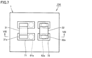
- FIGS. 7 to 8 A perspective plan view of the resin multilayer substrate 104 in the present embodiment is shown in FIG.
- FIG. 8 is a cross-sectional view taken along the line VIII-VIII in FIG.
- the conductor pattern 71 is disposed so as to abut the lower surface of the first component terminal 31 a of the first component 31, and the planar conductor pattern 71 is the first component 31.
- the wiring is pulled out from the side.
- the conductor via 61 a as the second conductor via is connected to the lower surface of the conductor pattern 71.
- the conductor via 61a as the second conductor via is electrically connected to the first component terminal 31a via the conductor pattern 71, but is not directly connected, Moreover, when it sees from the lamination direction of the laminated body 1, it does not necessarily exist in the position which overlaps with the 1st component terminal 31a.
- the conductor via 61b as the first conductor via is located at a position overlapping the first component terminal 31a.
- a conductor via 61c is connected to the lower end of the conductor via 61b via a conductor pattern 71b.
- a conductor via 61d is connected to the lower end of the conductor via 61c via a conductor pattern 71c.
- a conductor pattern 71d is connected to the lower end of the conductor via 61d.
- the conductor vias 61b, 61c, 61d as the first conductor vias are arranged linearly and continuously.
- the conductor pattern 72 is disposed so as to contact the lower surface of the second component terminal 32 a of the second component 32.
- the conductor via 62 a is connected to the lower surface of the conductor pattern 72.
- a conductor via 62b is connected to the lower end of the conductor via 62a via a conductor pattern 72a.
- a conductor via 62c is connected to the lower end of the conductor via 62b via a conductor pattern 72b.
- a conductor via 62d is connected to the lower end of the conductor via 62c via a conductor pattern 72c.
- a conductor pattern 72d is connected to the lower end of the conductor via 62d.
- FIG. 10 is a cross-sectional view taken along the line XX in FIG.
- the resin multilayer substrate 105 according to the present embodiment has a structure similar to that of the third embodiment. However, when viewed in a plan view, the two serial via portions connected to the first component 31 and the second component 32. It is asymmetrical with the two serial via portions connected to each other.
- FIG. 12 is a cross-sectional view taken along the line XII-XII in FIG.
- the resin multilayer substrate 106 includes a laminate 1 in which a plurality of resin layers 2 mainly composed of a thermoplastic resin are laminated, and a first component terminal 31a that is built in the laminate 1 and includes a first component terminal 31a.
- a conductor via 61a as a plurality of first conductor vias that are electrically connected to one component 31 and the first component terminal 31a and overlap the first component terminal 31a when viewed from the stacking direction of the multilayer body 1.
- 61c, 61d, and second conductor vias that are different in height from the first conductor vias while being shifted from the first conductor vias in a direction perpendicular to the stacking direction, and are electrically connected to the first conductor vias.
- Conductor via 61b is a plurality of resin layers 2 mainly composed of a thermoplastic resin are laminated, and a first component terminal 31a that is built in the laminate 1 and includes a first component terminal 31a.
- a conductor via 61a as a plurality of
- the first component terminal 31a and the conductor via 61a as the first conductor via are directly connected without a planar conductor pattern therebetween.
- a conductor pattern 71a is connected to the lower end of the conductor via 61a, and the conductor pattern 71a extends laterally.
- a conductor via 61b as a second conductor via is connected to the lower surface of the conductor pattern 71a.
- a conductor pattern 71b is connected to the lower end of the conductor via 61b.
- a conductor via 61c is connected to the lower surface of the conductor pattern 71b.
- a conductor via 61d is connected to the lower end of the conductor via 61c via a conductor pattern 71c.
- a conductor pattern 71d is connected to the lower end of the conductor via 61d.
- the conductor vias 61c and 61d are positioned so as to overlap with the conductor via 61a when viewed in a plan view.
- the conductor via 61b is in a position that does not overlap with the conductor vias 61a, 61c, 61d when viewed in a plan view.
- the conductor vias 61a, 61c, 61d correspond to the first conductor via.
- the number of conductor vias corresponding to the first conductor via may be plural.
- the number of conductor vias corresponding to the first conductor via is not limited to 3, and may be 2 or 4 or more.
- the built-in component is a rectangular parallelepiped and has a structure having external electrodes as terminals at both ends, but the structure of the built-in component is not limited to this.
- the size of the first part and the second part may be the same or different. The same applies to the shapes of the first part and the second part.
Landscapes
- Engineering & Computer Science (AREA)
- Microelectronics & Electronic Packaging (AREA)
- Manufacturing & Machinery (AREA)
- Physics & Mathematics (AREA)
- Electromagnetism (AREA)
- Production Of Multi-Layered Print Wiring Board (AREA)
Abstract
樹脂多層基板(101)は、熱可塑性樹脂を主材料とする複数の樹脂層(2)を積層したものである積層体(1)と、積層体(1)に内蔵され、第1部品端子を有する第1部品(31)と、積層体(1)に内蔵され、第2部品端子を有し、積層体(1)の積層方向から見たとき第1部品(31)から離隔するように配置された第2部品(32)と、前記第1部品端子に電気的に接続されており、積層体(1)の積層方向から見たとき前記第1部品端子と重なる位置にある第1導体ビアとしての導体ビア(61a)と、第1導体ビア(61a)から第2部品(32)側にずれつつ第1導体ビアとは異なる高さにあり、第1導体ビアに電気的に接続された複数の第2導体ビア(61b)とを備える。
Description
本発明は、樹脂多層基板に関するものである。
熱可塑性樹脂のフィルムを積み重ねて積層体を形成し、これを一体化することにより樹脂多層基板を得ることが知られている。樹脂多層基板に部品を内蔵する場合がある。その一例が特開2003-86949号公報(特許文献1)に記載されている。内蔵された部品から配線を引き出す際に、複数の導体ビアが積層方向に沿って直列に接続された構造(以下「直列ビア部」という。)が用いられる場合がある。
直列ビア部では、導体ビアと導体パターンとが交互に連なるようにして電気的に接続される。直列ビア部では、導体ビアと導体パターンとの間の断線が問題となる。積層体の中で直列ビア部は他の部分(樹脂層)に比べて剛性が高いので、積層体を一体化するために加圧された際に、積層体の最表面のコプラナリティが悪化する場合がある。最表面のコプラナリティが悪化すると、のちに表面に部品を実装しようとしたときに正しく実装できなくなる場合がある。内蔵部品同士の間隔が狭く設定されている場合、積層体の一体化のための加圧などの際に直列ビア部の形がゆがみ、複数の直列ビア部の間で互いに接触して短絡が生じるおそれがある。また、内蔵部品も積層体内の樹脂層に比べて剛性が高いので、同様の理由によって部品同士の接触による短絡も問題となる。
なお、直列ビア部、内蔵部品などは、剛性が高いので、積層体を一体化するために加圧された際に、直列ビア部、内蔵部品などが配置されている部分において積層体の最表面のコプラナリティが悪化する場合がある。最表面のコプラナリティが悪化すると、のちに最表面に部品を実装しようとしたときに正しく実装できなくなる場合がある。
そこで、本発明は、これらの問題のうち少なくとも1つを軽減することができる樹脂多層基板を提供することを目的とする。
上記目的を達成するため、本発明に基づく樹脂多層基板は、熱可塑性樹脂を主材料とする複数の樹脂層を積層したものである積層体と、上記積層体に内蔵され、第1部品端子を有する第1部品と、上記積層体に内蔵され、第2部品端子を有し、上記積層体の積層方向から見たとき上記第1部品から離隔するように配置された第2部品と、上記第1部品端子に電気的に接続されており、上記積層体の積層方向から見たとき上記第1部品端子と重なる位置にある第1導体ビアと、上記第1導体ビアから上記第2部品側にずれつつ上記第1導体ビアとは異なる高さにあり、上記第1導体ビアに電気的に接続された複数の第2導体ビアとを備える。
本発明によれば、直列ビア部のゆがみまたは傾きによる、直列ビア部同士の接触による短絡または部品同士の接触による短絡を防止することができる。直列ビア部が全体として柔軟性を有することとなる結果、直列ビア部の断線を防止することができる。
図面において示す寸法比は、必ずしも忠実に現実のとおりを表しているとは限らず、説明の便宜のために寸法比を誇張して示している場合がある。以下の説明において、上または下の概念に言及する際には、絶対的な上または下を意味するとは限らず、図示された姿勢の中での相対的な上または下を意味する場合がある。
(実施の形態1)
図1~図2を参照して、本発明に基づく実施の形態1における樹脂多層基板について説明する。本実施の形態における樹脂多層基板101の透視平面図を図1に示す。樹脂多層基板101を単純に上、すなわち積層方向の一方の側から見たときには樹脂層に覆われて内蔵部品は見えないが、図1では説明の便宜のために、樹脂層に覆われて隠されている第1部品31、第2部品32、導体パターン71aなどが見えるように表示している。以下の実施の形態で示す平面図についても同様である。図1におけるII-II線に関する矢視断面図を図2に示す。
図1~図2を参照して、本発明に基づく実施の形態1における樹脂多層基板について説明する。本実施の形態における樹脂多層基板101の透視平面図を図1に示す。樹脂多層基板101を単純に上、すなわち積層方向の一方の側から見たときには樹脂層に覆われて内蔵部品は見えないが、図1では説明の便宜のために、樹脂層に覆われて隠されている第1部品31、第2部品32、導体パターン71aなどが見えるように表示している。以下の実施の形態で示す平面図についても同様である。図1におけるII-II線に関する矢視断面図を図2に示す。
本実施の形態における樹脂多層基板101は、熱可塑性樹脂を主材料とする複数の樹脂層2を積層したものである積層体1と、積層体1に内蔵され、第1部品端子31aを有する第1部品31と、積層体1に内蔵され、第2部品端子32aを有し、積層体1の積層方向から見たとき第1部品31から離隔するように配置された第2部品32と、第1部品端子31aに電気的に接続されており、積層体1の積層方向から見たとき第1部品端子31aと重なる位置にある第1導体ビアとしての導体ビア61aと、第1導体ビアから第2部品32側にずれつつ第1導体ビアとは異なる高さにあり、第1導体ビアに電気的に接続された複数の第2導体ビアとしての導体ビア61b,61c,61dとを備える。
第1部品端子31aと第1導体ビアとしての導体ビア61aとは、間に平面状の導体パターンを介さずに直接的に接続されている。導体ビア61aの下端には、平面状の導体パターン71aが接続されており、導体パターン71aの下面には導体ビア61bが接続されている。すなわち、平面状の導体パターン71aは、第1導体ビアとしての導体ビア61aと、第1導体ビアから第2部品32側にずれた第2導体ビアとしての導体ビア61bとを接続するための引き出し導体として機能する。第2導体ビアとしての導体ビア61bの下端には、導体パターン71bを介して導体ビア61cが接続されている。さらに導体ビア61cの下端には、導体パターン71cを介して導体ビア61dが接続されている。導体ビア61dの下端には、導体パターン71dが接続されている。導体ビア61c,61dも第2導体ビアに該当する。導体パターン71b,71c,71dは導体ビア同士を接続するためのパッド導体として機能する。また、これにより第2導体ビアとしての導体ビア61b,61c,61dは直線的に連続する。なお、第2導体ビアの個数は3に限らず、2または4以上であってもよい。
本実施の形態では、第1部品31から第1導体ビアとしての導体ビア61aおよび第2導体ビアとしての導体ビア61b,61c,61dを含む形の直列ビア部が引き出されているが、第2導体ビアとしての導体ビア61b,61c,61dが第1導体ビアとしての導体ビア61aに比べて第2部品32側にずれているので、積層体1の他の部分に比べて剛性が高い直列ビア部が第1部品31と積層方向に重なることを抑制できる。また、本実施の形態では、直列ビア部の一部が、積層方向から見たとき第1部品31と第2部品32との間に位置している。したがって、積層体の一体化のための加圧などの際に、積層体内にかかる圧力がアンバランスになることを抑制できる。すなわち、部品(第1部品31、第2部品32)、直列ビア部などは、積層体1の他の部分(樹脂層など)に比べて剛性が高く、積層体の一体化のための加圧などの際に、積層体内にかかる圧力がアンバランスになりやすいが、剛性が高い部分の一部を複数の部品(第1部品31、第2部品32)間に配置することによりバランスさせることができる。これにより、直列ビア部が傾くことなどによって直列ビア部同士が接触したり、部品が傾くことなどによって部品同士が接触したりすることを防止することができる。したがって、不所望な短絡を防止することができる。
また、直列ビア部の一部を積層方向から見て重ならないようにすることで積層体の最表面のコプラナリティの悪化度合いを低減することができる。
本実施の形態では、直列ビア部が厚み方向にのみ連なるのではなく、直列ビア部の途中で第2導体ビアとしての導体ビア61b,61c,61dが第1導体ビアとしての導体ビア61aに比べて第2部品32側にずれているので、直列ビア部が全体としてばねのように柔軟性を有することとなる。直列ビア部が全体として柔軟性を有することにより、直列ビア部に過剰な負荷がかかることをなるべく避けることができ、過剰な負荷による断線をなるべく避けることができる。
本実施の形態で示したように、第1導体ビアと第2導体ビアとの間に少なくとも1つの平面状導体パターンが介在していることが好ましい。この構成を採用することにより、第2導体ビアの位置を第1導体ビアの位置に比べて容易にずらすことができる。
(実施の形態2)
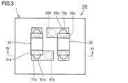
図3~図4を参照して、本発明に基づく実施の形態2における樹脂多層基板について説明する。本実施の形態における樹脂多層基板102の透視平面図を図3に示す。図3におけるIV-IV線に関する矢視断面図を図4に示す。
図3~図4を参照して、本発明に基づく実施の形態2における樹脂多層基板について説明する。本実施の形態における樹脂多層基板102の透視平面図を図3に示す。図3におけるIV-IV線に関する矢視断面図を図4に示す。
本実施の形態における樹脂多層基板102は、熱可塑性樹脂を主材料とする複数の樹脂層2を積層したものである積層体1と、積層体1に内蔵され、第1部品端子31aを有する第1部品31と、積層体1に内蔵され、第2部品端子32aを有し、積層体の積層方向から見たとき第1部品31から離隔するように配置された第2部品32と、第1部品端子31aに電気的に接続されており、積層体1の積層方向から見たとき第1部品端子31aと重なる位置にある複数の第1導体ビアとしての導体ビア61a,61c,61dと、第1導体ビアから第2部品32側にずれつつ第1導体ビアとは異なる高さにあり、第1導体ビアに電気的に接続された第2導体ビアとしての導体ビア61bとを備える。これにより、第1導体ビアとしての導体ビア61a,61c,61dは非連続ではあるが、直線的に配置される。
樹脂多層基板102は、第3導体ビア62aをさらに備える。第3導体ビア62aは、第2部品端子32aに電気的に接続されており、積層体1の積層方向から見たとき第2部品端子32aと重なる位置にある。第3導体ビア62aの第2部品端子32aに接続されているのと反対側の端は、導体パターン72aに接続されている。
樹脂多層基板102は、第3導体ビアとしての導体ビア62aから第1部品31側にずれつつ第3導体ビアとは異なる高さにあり、第3導体ビアに電気的に接続された第4導体ビアとしての導体ビア62bをさらに備えることが好ましい。この場合、複数の第4導体ビアが存在することが好ましい。すなわち、第4導体ビアとして複数の導体ビア62bが直列ビア部を構成していることが好ましい。
ここでは、第3導体ビアおよび第4導体ビアの存在に言及したが、第3導体ビアと第4導体ビアとの間でも、既に述べた第1導体ビアと第2導体ビアとの関係が成り立っていてもよい。たとえば後述する図5および図6に示されるような構成であってもよい。
樹脂多層基板102では、図3に示すように、第1部品31およびこれに接続された直列ビア部は、平面図においてL字形状となっている。第2部品32およびこれに接続された直列ビア部も同様である。2つのL字形状は点対称な位置関係で互いに組み合わさって配置されている。
本実施の形態では、導体ビア61a,61c,61dは重なっており、かつこれらの導体ビアは第1部品31にも重なっているので、このままであれば圧力がアンバランスになりやすい。しかし、途中で第2部品32の側にずれた導体ビア61bがあるので、圧力をバランスさせることができたり、コプラナリティを改善したりすることができる。
また、本実施の形態では、第1部品31に接続された直列ビア部だけでなく第2部品32に接続された直列ビア部においても途中で位置をずらす部分があるので、積層体の一体化のための加圧などの際に、積層体内にかかる圧力がアンバランスになることを抑制できる。したがって、部品同士の接触による短絡を防止することができる。本実施の形態では、第1部品31の直列ビア部だけでなく第2部品の直列ビア部も柔軟性を有することとなるので、直列ビア部に過剰な負荷がかかることをなるべく避けることができ、過剰な負荷による断線をなるべく避けることができる。
(実施の形態3)
図5~図6を参照して、本発明に基づく実施の形態3における樹脂多層基板について説明する。本実施の形態における樹脂多層基板103の透視平面図を図5に示す。図5におけるVI-VI線に関する矢視断面図を図6に示す。本実施の形態では、2つの内蔵部品の合計4つの端子からそれぞれ直列ビア部が引き出されている。
図5~図6を参照して、本発明に基づく実施の形態3における樹脂多層基板について説明する。本実施の形態における樹脂多層基板103の透視平面図を図5に示す。図5におけるVI-VI線に関する矢視断面図を図6に示す。本実施の形態では、2つの内蔵部品の合計4つの端子からそれぞれ直列ビア部が引き出されている。
本実施の形態では、図5に示すように、第1部品31およびこれに接続された2つの直列ビア部は、平面図においてコの字形状となっている。第2部品32およびこれに接続された2つの直列ビア部も同様である。2つのコの字形状は対称な位置関係で互いに対向して配置されている。
本実施の形態においても、実施の形態2と同様の効果を得ることができる。
(実施の形態4)
図7~図8を参照して、本発明に基づく実施の形態4における樹脂多層基板について説明する。本実施の形態における樹脂多層基板104の透視平面図を図7に示す。図7におけるVIII-VIII線に関する矢視断面図を図8に示す。
(実施の形態4)
図7~図8を参照して、本発明に基づく実施の形態4における樹脂多層基板について説明する。本実施の形態における樹脂多層基板104の透視平面図を図7に示す。図7におけるVIII-VIII線に関する矢視断面図を図8に示す。
本実施の形態では、図8に示すように、導体パターン71が第1部品31の第1部品端子31aの下面に当接するように配置されており、平面状の導体パターン71が第1部品31から配線を側方に引き出す構造となっている。第2導体ビアとしての導体ビア61aは導体パターン71の下面に接続されている。本実施の形態では、第2導体ビアとしての導体ビア61aは、導体パターン71を介して第1部品端子31aに電気的に接続された状態にあるが、直接的には接続されておらず、また、積層体1の積層方向から見たとき第1部品端子31aと重なる位置にあるわけではない。導体ビア61aの下端からは導体パターン71aによって配線は側方に引き出され、その結果、再び、第1部品端子31aと重なる位置に戻されている。第1導体ビアとしての導体ビア61bは、第1部品端子31aと重なる位置にある。導体ビア61bの下端には、導体パターン71bを介して導体ビア61cが接続されている。導体ビア61cの下端には、導体パターン71cを介して導体ビア61dが接続されている。導体ビア61dの下端には、導体パターン71dが接続されている。第1導体ビアとしての導体ビア61b,61c,61dは、直線的に連続して配置されている。
導体パターン72が第2部品32の第2部品端子32aの下面に当接するように配置されている。導体ビア62aは導体パターン72の下面に接続されている。導体ビア62aの下端には、導体パターン72aを介して導体ビア62bが接続されている。導体ビア62bの下端には、導体パターン72bを介して導体ビア62cが接続されている。導体ビア62cの下端には、導体パターン72cを介して導体ビア62dが接続されている。導体ビア62dの下端には、導体パターン72dが接続されている。
本実施の形態においても、実施の形態2と同様の効果を得ることができる。
(実施の形態5)
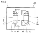
図9~図10を参照して、本発明に基づく実施の形態5における樹脂多層基板について説明する。本実施の形態における樹脂多層基板105の透視平面図を図9に示す。図9におけるX-X線に関する矢視断面図を図10に示す。
(実施の形態5)
図9~図10を参照して、本発明に基づく実施の形態5における樹脂多層基板について説明する。本実施の形態における樹脂多層基板105の透視平面図を図9に示す。図9におけるX-X線に関する矢視断面図を図10に示す。
本実施の形態における樹脂多層基板105は、実施の形態3と類似した構造となっているが、平面図で見たとき、第1部品31に接続された2つの直列ビア部と第2部品32に接続された2つの直列ビア部とで、非対称となっている。
本実施の形態においても、実施の形態3と同様の効果を得ることができる。
(実施の形態6)
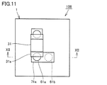
図11~図12を参照して、本発明に基づく実施の形態6における樹脂多層基板について説明する。本実施の形態における樹脂多層基板106の透視平面図を図11に示す。図11におけるXII-XII線に関する矢視断面図を図12に示す。
(実施の形態6)
図11~図12を参照して、本発明に基づく実施の形態6における樹脂多層基板について説明する。本実施の形態における樹脂多層基板106の透視平面図を図11に示す。図11におけるXII-XII線に関する矢視断面図を図12に示す。
本実施の形態における樹脂多層基板106は、熱可塑性樹脂を主材料とする複数の樹脂層2を積層したものである積層体1と、積層体1に内蔵され、第1部品端子31aを有する第1部品31と、第1部品端子31aに電気的に接続されており、積層体1の積層方向から見たとき第1部品端子31aと重なる位置にある複数の第1導体ビアとしての導体ビア61a,61c,61dと、第1導体ビアから前記積層方向とは垂直な方向にずれつつ第1導体ビアとは異なる高さにあり、第1導体ビアに電気的に接続された第2導体ビアとしての導体ビア61bとを備える。
第1部品端子31aと第1導体ビアとしての導体ビア61aとは、間に平面状の導体パターンを介さずに直接的に接続されている。導体ビア61aの下端には導体パターン71aが接続されており、導体パターン71aは側方に延在している。導体パターン71aの下面には第2導体ビアとしての導体ビア61bが接続されている。導体ビア61bの下端には導体パターン71bが接続されている。導体パターン71bの下面には導体ビア61cが接続されている。導体ビア61cの下端には導体パターン71cを介して導体ビア61dが接続されている。導体ビア61dの下端には導体パターン71dが接続されている。導体ビア61c,61dは、平面図で見たときに導体ビア61aと重なる位置にある。導体ビア61bは、平面図で見たときに導体ビア61a,61c,61dと重ならない位置にある。この例では導体ビア61a,61c,61dが第1導体ビアに該当する。第1導体ビアに該当する導体ビアの個数は複数であればよい。第1導体ビアに該当する導体ビアの個数は3に限らず、2でもよく4以上であってもよい。
本実施の形態においては、第1部品31と積層体1内の他の要素との短絡を防止することができる。
なお、上記各実施の形態では、内蔵部品が1個または2個である例を示したが、内蔵部品の数は3個以上であってもよい。
上記各実施の形態では、内蔵部品は直方体であって両端に端子としての外部電極を備える構造のものとしたが、内蔵部品の構造はこれに限らない。
第1部品および第2部品のサイズは、同じであってもよく、異なっていてもよい。第1部品および第2部品の形状についても同様である。
なお、上記実施の形態のうち複数を適宜組み合わせて採用してもよい。
なお、今回開示した上記実施の形態はすべての点で例示であって制限的なものではない。本発明の範囲は上記した説明ではなくて請求の範囲によって示され、請求の範囲と均等の意味および範囲内でのすべての変更を含むものである。
なお、今回開示した上記実施の形態はすべての点で例示であって制限的なものではない。本発明の範囲は上記した説明ではなくて請求の範囲によって示され、請求の範囲と均等の意味および範囲内でのすべての変更を含むものである。
2 樹脂層、30 部品、30a 部品端子、31 第1部品、31a 第1部品端子、32 第2部品、32a 第2部品端子、61a,61b,61c,61d 導体ビア、62a,62b,62c,62d 導体ビア、71a,71b,71c,71d,72a,72b,72c,72d 導体パターン、101,102,103,104,105,106 樹脂多層基板。
Claims (6)
- 熱可塑性樹脂を主材料とする複数の樹脂層を積層したものである積層体と、
前記積層体に内蔵され、第1部品端子を有する第1部品と、
前記積層体に内蔵され、第2部品端子を有し、前記積層体の積層方向から見たとき前記第1部品から離隔するように配置された第2部品と、
前記第1部品端子に電気的に接続されており、前記積層体の積層方向から見たとき前記第1部品端子と重なる位置にある第1導体ビアと、
前記第1導体ビアから前記第2部品側にずれつつ前記第1導体ビアとは異なる高さにあり、前記第1導体ビアに電気的に接続された複数の第2導体ビアとを備える、樹脂多層基板。 - 熱可塑性樹脂を主材料とする複数の樹脂層を積層したものである積層体と、
前記積層体に内蔵され、第1部品端子を有する第1部品と、
前記積層体に内蔵され、第2部品端子を有し、前記積層体の積層方向から見たとき前記第1部品から離隔するように配置された第2部品と、
前記第1部品端子に電気的に接続されており、前記積層体の積層方向から見たとき前記第1部品端子と重なる位置にある複数の第1導体ビアと、
前記第1導体ビアから前記第2部品側にずれつつ前記第1導体ビアとは異なる高さにあり、前記第1導体ビアに電気的に接続された第2導体ビアとを備える、樹脂多層基板。 - 前記第1導体ビアと前記第2導体ビアとの間に少なくとも1つの平面状導体パターンが介在している、請求項1または2に記載の樹脂多層基板。
- 前記第2部品端子に電気的に接続されており、前記積層体の積層方向から見たとき前記第2部品端子と重なる位置にある第3導体ビアをさらに備える、請求項1から3のいずれかに記載の樹脂多層基板。
- 前記第3導体ビアから前記第1部品側にずれつつ前記第3導体ビアとは異なる高さにあり、前記第3導体ビアに電気的に接続された第4導体ビアをさらに備える、請求項4に記載の樹脂多層基板。
- 熱可塑性樹脂を主材料とする複数の樹脂層を積層したものである積層体と、
前記積層体に内蔵され、第1部品端子を有する第1部品と、
前記第1部品端子に電気的に接続されており、前記積層体の積層方向から見たとき前記第1部品端子と重なる位置にある複数の第1導体ビアと、
前記第1導体ビアから前記積層方向とは垂直な方向にずれつつ前記第1導体ビアとは異なる高さにあり、前記第1導体ビアに電気的に接続された第2導体ビアとを備える、樹脂多層基板。
Priority Applications (2)
| Application Number | Priority Date | Filing Date | Title |
|---|---|---|---|
| CN201790000864.0U CN209358846U (zh) | 2016-06-02 | 2017-04-28 | 树脂多层基板 |
| US16/180,054 US10524352B2 (en) | 2016-06-02 | 2018-11-05 | Resin multilayer substrate |
Applications Claiming Priority (2)
| Application Number | Priority Date | Filing Date | Title |
|---|---|---|---|
| JP2016-111169 | 2016-06-02 | ||
| JP2016111169 | 2016-06-02 |
Related Child Applications (1)
| Application Number | Title | Priority Date | Filing Date |
|---|---|---|---|
| US16/180,054 Continuation US10524352B2 (en) | 2016-06-02 | 2018-11-05 | Resin multilayer substrate |
Publications (1)
| Publication Number | Publication Date |
|---|---|
| WO2017208713A1 true WO2017208713A1 (ja) | 2017-12-07 |
Family
ID=60479533
Family Applications (1)
| Application Number | Title | Priority Date | Filing Date |
|---|---|---|---|
| PCT/JP2017/016974 Ceased WO2017208713A1 (ja) | 2016-06-02 | 2017-04-28 | 樹脂多層基板 |
Country Status (3)
| Country | Link |
|---|---|
| US (1) | US10524352B2 (ja) |
| CN (1) | CN209358846U (ja) |
| WO (1) | WO2017208713A1 (ja) |
Citations (2)
| Publication number | Priority date | Publication date | Assignee | Title |
|---|---|---|---|---|
| JP2003086949A (ja) * | 2001-06-13 | 2003-03-20 | Denso Corp | プリント基板の製造方法およびその製造方法によって形成されるプリント基板 |
| JP2003347738A (ja) * | 2002-05-30 | 2003-12-05 | Denso Corp | 多層配線基板及びその製造方法 |
Family Cites Families (3)
| Publication number | Priority date | Publication date | Assignee | Title |
|---|---|---|---|---|
| KR100488412B1 (ko) | 2001-06-13 | 2005-05-11 | 가부시키가이샤 덴소 | 내장된 전기소자를 갖는 인쇄 배선 기판 및 그 제조 방법 |
| JP5402939B2 (ja) * | 2008-10-27 | 2014-01-29 | 日立化成株式会社 | 銅の表面処理方法及び銅 |
| TWI446497B (zh) * | 2010-08-13 | 2014-07-21 | 欣興電子股份有限公司 | 嵌埋被動元件之封裝基板及其製法 |
-
2017
- 2017-04-28 CN CN201790000864.0U patent/CN209358846U/zh active Active
- 2017-04-28 WO PCT/JP2017/016974 patent/WO2017208713A1/ja not_active Ceased
-
2018
- 2018-11-05 US US16/180,054 patent/US10524352B2/en active Active
Patent Citations (2)
| Publication number | Priority date | Publication date | Assignee | Title |
|---|---|---|---|---|
| JP2003086949A (ja) * | 2001-06-13 | 2003-03-20 | Denso Corp | プリント基板の製造方法およびその製造方法によって形成されるプリント基板 |
| JP2003347738A (ja) * | 2002-05-30 | 2003-12-05 | Denso Corp | 多層配線基板及びその製造方法 |
Also Published As
| Publication number | Publication date |
|---|---|
| US20190075649A1 (en) | 2019-03-07 |
| US10524352B2 (en) | 2019-12-31 |
| CN209358846U (zh) | 2019-09-06 |
Similar Documents
| Publication | Publication Date | Title |
|---|---|---|
| KR101656294B1 (ko) | 전자부품 | |
| JP5888281B2 (ja) | 実装ランド構造体及び積層コンデンサの実装構造体 | |
| WO2017159284A1 (ja) | 多層基板及びその製造方法 | |
| JP2018170521A (ja) | 樹脂多層基板と回路基板の接合構造 | |
| JP6233524B2 (ja) | 部品内蔵基板 | |
| WO2015156141A1 (ja) | 部品内蔵多層基板 | |
| US9974185B2 (en) | Component-embedded substrate | |
| CN207802503U (zh) | 多层基板以及电子设备 | |
| WO2023238537A1 (ja) | モジュール | |
| US10271423B2 (en) | Flexible substrate | |
| CN107958875B (zh) | 半导体装置以及布线基板的设计方法 | |
| JP6562076B2 (ja) | 樹脂基板、部品搭載樹脂基板およびその製造方法 | |
| WO2017208713A1 (ja) | 樹脂多層基板 | |
| JPWO2017026208A1 (ja) | 樹脂多層基板およびその製造方法 | |
| JP6477894B2 (ja) | 樹脂回路基板、部品搭載樹脂回路基板 | |
| CN115116697B (zh) | 层叠线圈部件 | |
| US20250168978A1 (en) | Electronic component | |
| WO2018159839A1 (ja) | 樹脂多層基板および電子機器 | |
| JP2016012668A (ja) | 樹脂基板及び樹脂基板の製造方法 | |
| TWI646871B (zh) | 多層電路板 | |
| JP4461968B2 (ja) | 半導体発光装置 | |
| JP6251979B2 (ja) | 樹脂多層基板 | |
| JPWO2024262253A5 (ja) | ||
| JP2021044583A (ja) | 半導体装置 | |
| JP2022144852A (ja) | 積層コイル部品 |
Legal Events
| Date | Code | Title | Description |
|---|---|---|---|
| NENP | Non-entry into the national phase |
Ref country code: DE |
|
| 121 | Ep: the epo has been informed by wipo that ep was designated in this application |
Ref document number: 17806272 Country of ref document: EP Kind code of ref document: A1 |
|
| 122 | Ep: pct application non-entry in european phase |
Ref document number: 17806272 Country of ref document: EP Kind code of ref document: A1 |
|
| NENP | Non-entry into the national phase |
Ref country code: JP |