WO2017204522A1 - 고효율 장파장 발광 소자 - Google Patents
고효율 장파장 발광 소자 Download PDFInfo
- Publication number
- WO2017204522A1 WO2017204522A1 PCT/KR2017/005333 KR2017005333W WO2017204522A1 WO 2017204522 A1 WO2017204522 A1 WO 2017204522A1 KR 2017005333 W KR2017005333 W KR 2017005333W WO 2017204522 A1 WO2017204522 A1 WO 2017204522A1
- Authority
- WO
- WIPO (PCT)
- Prior art keywords
- layer
- barrier
- doped
- well
- emitting device
- Prior art date
- Legal status (The legal status is an assumption and is not a legal conclusion. Google has not performed a legal analysis and makes no representation as to the accuracy of the status listed.)
- Ceased
Links
Images




Classifications
-
- H—ELECTRICITY
- H10—SEMICONDUCTOR DEVICES; ELECTRIC SOLID-STATE DEVICES NOT OTHERWISE PROVIDED FOR
- H10H—INORGANIC LIGHT-EMITTING SEMICONDUCTOR DEVICES HAVING POTENTIAL BARRIERS
- H10H20/00—Individual inorganic light-emitting semiconductor devices having potential barriers, e.g. light-emitting diodes [LED]
- H10H20/80—Constructional details
- H10H20/81—Bodies
- H10H20/811—Bodies having quantum effect structures or superlattices, e.g. tunnel junctions
-
- H—ELECTRICITY
- H10—SEMICONDUCTOR DEVICES; ELECTRIC SOLID-STATE DEVICES NOT OTHERWISE PROVIDED FOR
- H10H—INORGANIC LIGHT-EMITTING SEMICONDUCTOR DEVICES HAVING POTENTIAL BARRIERS
- H10H20/00—Individual inorganic light-emitting semiconductor devices having potential barriers, e.g. light-emitting diodes [LED]
- H10H20/01—Manufacture or treatment
- H10H20/011—Manufacture or treatment of bodies, e.g. forming semiconductor layers
- H10H20/013—Manufacture or treatment of bodies, e.g. forming semiconductor layers having light-emitting regions comprising only Group III-V materials
- H10H20/0137—Manufacture or treatment of bodies, e.g. forming semiconductor layers having light-emitting regions comprising only Group III-V materials the light-emitting regions comprising nitride materials
-
- H—ELECTRICITY
- H10—SEMICONDUCTOR DEVICES; ELECTRIC SOLID-STATE DEVICES NOT OTHERWISE PROVIDED FOR
- H10H—INORGANIC LIGHT-EMITTING SEMICONDUCTOR DEVICES HAVING POTENTIAL BARRIERS
- H10H20/00—Individual inorganic light-emitting semiconductor devices having potential barriers, e.g. light-emitting diodes [LED]
- H10H20/80—Constructional details
- H10H20/81—Bodies
- H10H20/811—Bodies having quantum effect structures or superlattices, e.g. tunnel junctions
- H10H20/812—Bodies having quantum effect structures or superlattices, e.g. tunnel junctions within the light-emitting regions, e.g. having quantum confinement structures
-
- H—ELECTRICITY
- H10—SEMICONDUCTOR DEVICES; ELECTRIC SOLID-STATE DEVICES NOT OTHERWISE PROVIDED FOR
- H10H—INORGANIC LIGHT-EMITTING SEMICONDUCTOR DEVICES HAVING POTENTIAL BARRIERS
- H10H20/00—Individual inorganic light-emitting semiconductor devices having potential barriers, e.g. light-emitting diodes [LED]
- H10H20/80—Constructional details
- H10H20/81—Bodies
- H10H20/816—Bodies having carrier transport control structures, e.g. highly-doped semiconductor layers or current-blocking structures
- H10H20/8162—Current-blocking structures
-
- H—ELECTRICITY
- H10—SEMICONDUCTOR DEVICES; ELECTRIC SOLID-STATE DEVICES NOT OTHERWISE PROVIDED FOR
- H10H—INORGANIC LIGHT-EMITTING SEMICONDUCTOR DEVICES HAVING POTENTIAL BARRIERS
- H10H20/00—Individual inorganic light-emitting semiconductor devices having potential barriers, e.g. light-emitting diodes [LED]
- H10H20/80—Constructional details
- H10H20/81—Bodies
- H10H20/817—Bodies characterised by the crystal structures or orientations, e.g. polycrystalline, amorphous or porous
- H10H20/818—Bodies characterised by the crystal structures or orientations, e.g. polycrystalline, amorphous or porous within the light-emitting regions
-
- H—ELECTRICITY
- H10—SEMICONDUCTOR DEVICES; ELECTRIC SOLID-STATE DEVICES NOT OTHERWISE PROVIDED FOR
- H10H—INORGANIC LIGHT-EMITTING SEMICONDUCTOR DEVICES HAVING POTENTIAL BARRIERS
- H10H20/00—Individual inorganic light-emitting semiconductor devices having potential barriers, e.g. light-emitting diodes [LED]
- H10H20/80—Constructional details
- H10H20/81—Bodies
- H10H20/822—Materials of the light-emitting regions
-
- H—ELECTRICITY
- H10—SEMICONDUCTOR DEVICES; ELECTRIC SOLID-STATE DEVICES NOT OTHERWISE PROVIDED FOR
- H10H—INORGANIC LIGHT-EMITTING SEMICONDUCTOR DEVICES HAVING POTENTIAL BARRIERS
- H10H20/00—Individual inorganic light-emitting semiconductor devices having potential barriers, e.g. light-emitting diodes [LED]
- H10H20/80—Constructional details
- H10H20/81—Bodies
- H10H20/822—Materials of the light-emitting regions
- H10H20/824—Materials of the light-emitting regions comprising only Group III-V materials, e.g. GaP
- H10H20/825—Materials of the light-emitting regions comprising only Group III-V materials, e.g. GaP containing nitrogen, e.g. GaN
-
- H—ELECTRICITY
- H10—SEMICONDUCTOR DEVICES; ELECTRIC SOLID-STATE DEVICES NOT OTHERWISE PROVIDED FOR
- H10H—INORGANIC LIGHT-EMITTING SEMICONDUCTOR DEVICES HAVING POTENTIAL BARRIERS
- H10H20/00—Individual inorganic light-emitting semiconductor devices having potential barriers, e.g. light-emitting diodes [LED]
- H10H20/80—Constructional details
- H10H20/85—Packages
- H10H20/851—Wavelength conversion means
Definitions
- the present invention relates to light emitting devices, and more particularly, to high efficiency light emitting devices that emit light having a long wavelength including green light.
- nitride semiconductors are widely used as base materials of light emitting devices such as light emitting diodes.
- the nitride-based semiconductor may have various band gap energies according to the composition ratio of the group III element, thereby realizing light of various wavelength bands by controlling the composition ratio of elements such as Al, Ga, and In.
- a multi-quantum well structure is generally used as the active layer structure, and the emission wavelength of the light emitting device is determined according to the composition ratio of the nitride semiconductor of the well layer of the multi-quantum well structure.
- an InGaN layer including a small amount of In is used as a well layer in the case of a light emitting device emitting blue light from the active layer
- an AlGaN layer is used as a well layer in the case of an ultraviolet light emitting device.
- a well layer is formed using a nitride-based semiconductor including a large amount of In.
- nitride-based semiconductors containing an excessive amount of In, such as InGaN are different from GaN in growth conditions, and thus, it is difficult to apply a general blue light emitting device manufacturing method to a long wavelength light emitting device as it is.
- light emitting diodes having a well layer containing In in excess are generally known to be more vulnerable to electrostatic discharge than blue light emitting diodes.
- Another object of the present invention is to provide a long wavelength light emitting device having high luminous efficiency while preventing device defects caused by electrostatic discharge.
- a long wavelength light emitting device includes: a first conductivity type semiconductor layer; An active layer disposed on the first conductivity type semiconductor layer and having a quantum well structure; And a second conductivity type semiconductor layer on the active layer, wherein the active layer comprises: at least one well layer including a nitride based semiconductor including 21% or more of In; At least two barrier layers positioned above and below the well layer; And at least one upper capping layer positioned on the well layer and between the well layer and the barrier layer, wherein the upper capping layer has a greater bandgap energy than the barrier layer and the upper cap.
- the ping layer and the well layer are in contact.
- the well layer may include InGaN
- the barrier layer may include GaN
- the upper capping layer may include AlGaN.
- AlGaN of the upper capping layer may include 0.1% to 2.5% of Al. More specifically, the AlGaN of the upper capping layer may include Al of 1.4% to 1.8%, it can achieve a good light output and a low forward voltage in this range.
- the thickness of the upper capping layer may be thinner than the thickness of the barrier layer.
- the upper capping layer may have a thickness of 5 ⁇ to 20 ⁇ .
- the top barrier layer may include a sub barrier layer having a band gap energy less than the average band gap energy of the top barrier layer.
- the sub barrier layer may contain In, and the In composition ratio of the sub barrier layer may be smaller than the In composition ratio of the well layer.
- the sub barrier layer has a lattice constant smaller than that of the well layer, thus mitigating the lattice mismatch between the well layer and the electron blocking layer. Accordingly, the crystal quality of the second conductivity type semiconductor layer may be improved.
- the long wavelength light emitting device may further include at least one lower capping layer positioned below the well layer and disposed between the well layer and the barrier layer, wherein the lower capping layer has a larger band than the barrier layer. May have a gap energy.
- the long wavelength light emitting device may further include an electron blocking layer on the active layer.
- the electron blocking layer may include a grading layer in which an Al composition ratio decreases toward the second conductivity type semiconductor layer.
- an Al grading layer By using an Al grading layer, holes can be easily injected into the active layer while blocking electrons.
- the electron blocking layer may contain In, and the In composition ratio of the electron blocking layer may be smaller than the In composition ratio of the sub barrier layer. Accordingly, the In composition ratio gradually decreases and the lattice constant decreases in the order of the well layer, the sub barrier layer, and the electron blocking layer.
- the crystal quality of the electron blocking layer and the second conductive semiconductor layer may be improved by gradually decreasing the In composition ratio as described above. By improving the crystal quality of the second conductive semiconductor layer and the electron blocking layer, it is possible to provide a light emitting device that is also resistant to electrostatic discharge.
- the electron blocking layer may include a first electron blocking layer in contact with the active layer, a second electron blocking layer disposed on the first electron blocking layer, and a third electron blocking layer in contact with the second conductive semiconductor layer.
- the second electron blocking layer may have a higher concentration of Mg than the first and third electron blocking layers, and the third electron blocking layer may have a superlattice structure. Accordingly, the hole can be well injected into the active layer while efficiently blocking electrons using the second electron blocking layer.
- the third electron blocking layer may have a superlattice structure of AlInGaN / GaN.
- a superlattice structure of AlInGaN / GaN it is possible to improve the crystal quality of the second conductive semiconductor layer formed thereon, such as a GaN layer.
- the barrier layer may have a thickness of 120 ⁇ to 150 ⁇ , but is not limited thereto.
- the barrier layer may have a thickness thicker than 150 kPa.
- the barrier layer has a thickness of 220 kPa or less. If the barrier layer is thicker than 220 kV, the light output is reduced and the forward voltage is increased.
- the barrier layer may have a thickness of 170 kV to 200 kV, wherein high light output and low forward voltage are possible in this thickness range.
- the active layer includes a plurality of barrier layers and a plurality of well layers, wherein the plurality of barrier layers are relatively low concentration of the barrier layer and n-type impurities doped with a relatively high concentration of n-type impurities of the barrier layers And doped with undoped barrier layers. Barrier layers doped with a relatively high concentration of the n-type impurity are disposed closer to the first conductive semiconductor layer than the second conductive semiconductor layer. Electrons and holes are likely to recombine in the well layer, which is generally close to the second conductive string semiconductor layer.
- the barrier layers may include barrier layers doped with Mg, and the barrier layers doped with Mg may have a higher Mg doping concentration as they become closer to the second conductive semiconductor layer.
- the doping efficiency of the hole may be improved by doping Mg at a relatively high concentration to the barrier layers close to the second conductive semiconductor layer.
- the first conductivity type semiconductor layer may include a V-pit generation layer.
- the V-pit generation layer may include a first layer having a single composition doped with n-type impurity and a second layer having a superlattice structure.
- the first layer may be an n-type impurity doped GaN layer
- the second layer may have an InGaN / GaN superlattice structure.
- In content of InGaN in the superlattice structure may be 1% to 5%.
- the V-pit generation layer has a thickness of 1500 kPa to 3000 kPa, and the thickness of the second layer of the superlattice structure may be greater than or equal to the first layer of the single composition.
- the first conductivity type semiconductor layer may further include an n-type impurity modulation doping layer disposed under the V-pit generation layer, and the doping concentration of the n-type impurity modulation doping layer is n of the first layer. Higher than the impurity doping concentration.
- the n-type impurity modulation doped layer may be a contact layer in contact with the electrode.
- the second layer may be doped with n-type impurities at a higher concentration than the first layer.
- the second layer may be doped with n-type impurities at a lower concentration than the first layer, and may not be doped.
- the active layer includes a plurality of barrier layers and a plurality of well layers, wherein the plurality of barrier layers are relatively low concentration of the barrier layer and n-type impurities doped with a relatively high concentration of n-type impurities of the barrier layers Barrier layers doped with or doped with a relatively high concentration of the n-type impurity are disposed closer to the first conductivity-type semiconductor layer than the second conductivity-type semiconductor layer, and the first layer It has a higher n-type impurity doping concentration, and the first layer may have a relatively low-doped n-type impurity doping concentration or a higher n-type impurity doping concentration than the undoped barrier layers.
- the light emitting device can include V-pits whose inlet exceeds 250 nm.
- the second conductivity type semiconductor layer may include a p-AlGaN layer positioned between the p-GaN layers.
- the p-AlGaN layer may be disposed closer to the lower surface than the upper surface of the second conductive semiconductor layer, wherein the lower surface is a surface located closer to the active layer side than the upper surface.
- a long wavelength light emitting device which is positioned between the well layer and the barrier layer and comprises an upper capping layer covering the well layer.
- the upper capping layer prevents thermal damage of the well layer, thereby preventing the escape of In and preventing deterioration of the crystallinity of the well layer.
- the strain generated in the well layer may be reduced to reduce the quantum confinement stark effect, thereby improving luminous efficiency.
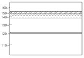
- 1 to 4 are cross-sectional views illustrating a long wavelength light emitting device and a method of manufacturing the long wavelength light emitting device according to the embodiments of the present invention.
- 5A and 5B are enlarged cross-sectional views and a band diagram for describing an active layer of a long wavelength light emitting device according to an embodiment.
- 6A and 6B are enlarged cross-sectional views and a band diagram for describing an active layer of a long wavelength light emitting device according to still another embodiment.
- FIG. 7 is an enlarged cross-sectional view illustrating a first conductive semiconductor layer of a long wavelength light emitting device according to an exemplary embodiment of the present invention.
- FIG. 8 is an enlarged cross-sectional view illustrating an electron blocking layer of a long wavelength light emitting device according to an exemplary embodiment of the present invention.
- FIG. 9 is an enlarged cross-sectional view illustrating an electron blocking layer of a long wavelength light emitting device according to still another embodiment of the present invention.
- FIG. 10 is an enlarged cross-sectional view illustrating a second conductivity-type semiconductor layer of a long wavelength light emitting device according to an exemplary embodiment of the present invention.
- FIG. 11 is optical photographs illustrating a surface of a light emitting device according to various embodiments of the present disclosure.
- each composition ratio, growth method, growth conditions, thickness, etc. for the nitride-based semiconductor layers described below are examples, and the present invention is not limited as described below.
- the composition ratio of In and Ga may be variously applied according to the needs of a person having ordinary skill in the art (hereinafter referred to as "normal technician").
- the nitride-based semiconductor layers described below may be grown using various methods generally known to those skilled in the art, for example, metal organic chemical vapor deposition (MOCVD), molecular beam epitaxy (MBE), or hybrid (HVPE). Vapor Phase Epitaxy) and the like can be grown using.
- MOCVD metal organic chemical vapor deposition
- MBE molecular beam epitaxy
- HVPE hybrid
- Vapor Phase Epitaxy Vapor Phase Epitaxy
- the semiconductor layers are described as being grown in the growth chamber using MOCVD.
- sources introduced into the growth chamber may use a source known to those skilled in the art, unless specifically mentioned.
- TMGa, TEGa, or the like may be used as a Ga source.
- TMAl and TEAl may be used as the Al source
- TMIn and TEIn may be used as the In source
- NH 3 may be used as the N source.
- the present invention is not limited thereto.
- the order of each step corresponds to an example, the order of each step may be changed.
- 1 to 4 are cross-sectional views illustrating a long wavelength light emitting device and a method of manufacturing the long wavelength light emitting device according to the embodiments of the present invention.
- the first conductive semiconductor layer 130 is formed on the substrate 110.
- a buffer layer may be further formed on the substrate 110 before the first conductivity-type semiconductor layer 130 is grown.
- the substrate 110 is not limited as long as it is a substrate capable of growing a nitride-based semiconductor, and may include, for example, a heterogeneous substrate such as a sapphire substrate, a silicon substrate, a silicon carbide substrate, or a spinel substrate. Homogeneous substrates such as substrates, aluminum nitride substrates, and the like. In addition, the substrate 110 may have a non-polar, semi-polar, or polar growth surface.
- the first conductivity type semiconductor layer 130 is located on the growth substrate 110.
- the first conductive semiconductor layer 130 may include a nitride based semiconductor such as (Al, Ga, In) N, and may be grown and formed on the growth substrate 110 using a method such as MOCVD, MBE, HVPE, or the like. have.
- MOCVD Metal Organic Chemical Vapor Deposition
- MBE Metal Organic Chemical Vapor Deposition
- HVPE high vacuum chemical vapor deposition
- the first conductivity is grown by growing a nitride-based semiconductor layer containing GaN at a predetermined growth rate at a growth temperature of about 950 ° C to 1200 ° C.
- the semiconductor layer 130 may be formed.
- the first conductivity-type semiconductor layer 120 may be doped n-type, including one or more impurities such as Si, C, Ge, Sn, Te, Pb.
- the present invention is not limited thereto, and the first conductive semiconductor layer 130 may be doped in a reverse conductivity type including a p-type dopant.
- the first conductivity-type semiconductor layer 130 may be formed of a single layer or multiple layers. When the first conductive semiconductor layer 130 is formed of multiple layers, the first conductive semiconductor layer 130 may include a superlattice layer, a contact layer, a modulation doping layer, an electron injection layer, and the like. A case in which the first conductive semiconductor layer 130 is a multilayer is described in more detail later with reference to FIG. 7.
- the buffer layer 120 may be further formed on the substrate 110 before the first conductivity type semiconductor layer 130 is grown.
- the buffer layer 120 may include a nitride semiconductor such as GaN, may be grown using MOCVD, and may be grown at a growth temperature in the range of about 450 to 600 ° C.
- the buffer layer 120 may make excellent crystallinity of semiconductor layers grown on the substrate 110 in a subsequent process, and may also serve as a seed layer on which nitride-based semiconductor layers may be grown on heterogeneous substrates. .
- an active layer 140 is formed on the first conductivity type semiconductor layer 130. Furthermore, the electron blocking layer 150 may be further formed on the active layer 140.
- the active layer 140 may include a nitride semiconductor such as (Al, Ga, In) N, and may be grown on the first conductivity type semiconductor layer 130 using a technique such as MOCVD, MBE, or HVPE. .
- the active layer 140 may include a quantum well structure (QW) including at least two barrier layers (141) and at least one well layer (143), and further, a plurality of barriers. It may include a multi-quantum well structure (MQW) including a layer 141 and a plurality of well layers 143.
- the active layer 140 is positioned on the top of the at least one well layer 143, the upper capping layer 145 or 145a interposed between the at least one well layer 143 and the barrier layer 141. It may further include. Further, the active layer 140 is positioned below the at least one well layer 143 to further include a lower capping layer 145b interposed between the at least one well layer 143 and the barrier layer 141. It may include.
- the light emitted from the active layer 140 may be light having a relatively long wavelength, for example, may emit green light having a longer wavelength band than blue light.
- the wavelength of the light emitted from the active layer 140 may be controlled by controlling the composition ratio of the nitride based semiconductor layer of the well layer 143.
- the well layer 143 may include a nitride-based semiconductor including In, and the composition ratio of In may be 21% or more.
- the active layer 140 will be described later in more detail.
- the second conductivity-type semiconductor layer 160 may include a nitride-based semiconductor such as (Al, Ga, In) N, and may be grown using a technique such as MOCVD, MBE, or HVPE.
- the second conductivity type semiconductor layer 160 may be doped in a conductivity type opposite to that of the first conductivity type semiconductor layer 130.
- the second conductivity-type semiconductor layer 160 may be doped with a p-type including impurities such as Mg.
- the second conductivity-type semiconductor layer 160 may be formed of a single p-GaN layer, but is not limited thereto, and may include an AlGaN layer therein.
- Mg doping concentration in the second conductivity-type semiconductor layer 160 may be the highest on the surface of the second conductivity-type semiconductor layer 160 and relatively high on the electron blocking layer 150 side, and may have a relatively low profile in the inner layer. have.
- the Mg doping concentration may include a region having a relatively low profile in the inner layer and a region having a relatively high doping concentration between the electron blocking layer 150 and a decrease.
- the AlGaN layer disposed inside the second conductivity-type semiconductor layer 160 may be disposed in a region having a relatively low Mg doping concentration and a region having a lower doping concentration between the electron blocking layer 150 and the region.
- the structure of FIG. 3 may be variously processed, and thus, a long wavelength light emitting device having various structures may be implemented.
- the long wavelength light emitting device may further include a first electrode 171 and a second electrode 173 to provide a horizontal light emitting device.
- the first electrode 171 and the second electrode 173 are electrically connected to the first conductive semiconductor layer 130 and the second conductive semiconductor layer 160, respectively.
- the present invention is not limited thereto, and the structure of FIG. 3 may be modified into various structures, such as a flip chip type light emitting device and a vertical type light emitting device.
- the substrate 110 may be omitted depending on the shape of the light emitting device.
- FIGS. 5A and 5B are enlarged cross-sectional views and band diagrams for describing an active layer 140 of a long wavelength light emitting device according to an exemplary embodiment.
- the active layer 140 may include at least one well layer 143, at least two barrier layers 141, and at least one upper capping layer 145.
- the active layer 140 includes a plurality of well layers 143 and a plurality of barrier layers 141 and upper portions of each of the plurality of well layers 143 and the plurality of well layers 143, respectively. It may include a plurality of upper capping layer 145 positioned in.
- the active layer 140 may include a top barrier layer 147 forming the last barrier layer of the active layer 140.
- the well layer 143 is located between the barrier layers 141, and the band gap energy of the well layer 143 is smaller than the band gap energy of the barrier layer 141, as shown in FIG. 5B.
- the well layer 143 may include or be formed of In x Ga (1-x) N (0 ⁇ x ⁇ 1), and the composition ratio x of In is controlled according to the wavelength emitted from the long wavelength light emitting device. Can be.
- the composition ratio x of In may be 0.21 or more, and further, 0.23 or more. Accordingly, the long wavelength light emitting device may emit green light.
- Barrier layer 141 may comprise GaN and / or InGaN.
- the upper capping layer 145 is positioned above the well layer 143 and is located between the well layer 143 and the barrier layer 141. In particular, the upper capping layer 145 may be in contact with the well layer 143 located below.
- the average lattice constant of the upper capping layer 145 may be smaller than the average lattice constant of the well layer 143 and the barrier layer 141.
- the bandgap energy of the upper capping layer 145 may be greater than the bandgap energy of the barrier layer 141.
- the upper capping layer 145 may include or be formed of Al y Ga (1-y) N (0 ⁇ y ⁇ 1), and the composition ratio y of Al may be 0.001 to 0.025. have. Additionally, when the composition ratio y of Al is in the range of 0.014 to 0.017, good light output and low forward voltage can be achieved.
- the barrier layer 141 may be formed on the first conductivity type semiconductor layer 130.
- the barrier layer 141 may be formed of GaN, and may be grown to a thickness of about 120 Pa to 220 Pa, and further, to about 170 Pa to 200 Pa at a temperature of about 900 ° C to 1200 ° C.
- the thickness of the barrier layer 141 can achieve high light output and low forward voltage in this range.
- the well layer 143 is formed on the barrier layer 141.
- the well layer 143 may be formed of In x Ga (1-x) N, and may be formed to a thickness of about 20 GPa to about 30 GPa.
- the growth temperature of the well layer 143 may be set at a temperature of about 150 ° C. to 200 ° C.
- an upper capping layer 145 is formed on the well layer 143.
- the upper capping layer 145 may be grown at a temperature substantially the same as the growth temperature of the well layer 143.
- the upper capping layer 145 may be formed of Al y Ga (1-y) N grown at a temperature of about 150 ° C. to 200 ° C. lower than the growth temperature of the barrier layer 141.
- the upper capping layer 145 may have a thickness of about 5 GPa to 20 GPa. Thereafter, the growth temperature may be increased again, and the growth of the barrier layer 141, the well layer 143, and the upper capping layer 145 may be repeated to provide an active layer 140 structure as illustrated in FIG. 5A. .
- the probability that In atoms in the well layer 143 are separated from the site of the semiconductor layer is high. Increases. In this case, In may precipitate or In segregation may occur on the surface of the well layer 143 as the growth temperature increases. In this case, the crystalline of the well layer 143 becomes coarse or the surface morphology deteriorates. In addition, when In atoms deviate from the site of the semiconductor layer, the In composition ratio of the well layer 143 becomes smaller than intended, so that light having a wavelength shorter than the intended wavelength is emitted from the light emitting device.
- the upper part is grown at the same temperature as the growth temperature of the well layer 143 without forming the barrier layer 141 by raising the temperature immediately after completion of the growth of the well layer 143.
- the barrier layer 141 is formed after the capping layer 145 is formed. Accordingly, the upper capping layer 145 may cover the upper portion of the well layer 143 to protect the well layer 143 from heat. Therefore, it is possible to prevent In atoms from escaping from the well layer 143, thereby preventing surface morphology deterioration of the well layer 143 and shifting of wavelengths to short wavelengths.
- the growth temperature of the barrier layer 141 may be increased to a temperature at which the crystallinity of the barrier layer 141 may be excellent, thereby improving the crystallinity of the entire active layer 140 to emit light.
- the luminous efficiency of the device can be improved.
- the upper capping layer 145 is formed of Al y Ga (1-y) N grown at a relatively low temperature, the crystallinity of the upper capping layer 145 itself may not be relatively excellent.
- the thickness of the upper capping layer 145 is controlled to about 5 kPa to 20 kPa, the thickness of the upper capping layer 145 is very thin compared to the barrier layer 141 so that almost all of the crystalline degradation of the active layer 140 due to the upper capping layer 145 occurs. I never do that. Therefore, a decrease in luminous efficiency due to crystalline of the upper capping layer 145 also hardly occurs.
- long wavelength light emitting devices such as green light emitting devices have relatively strong stress and strain due to the lattice constant difference between the well layer and the barrier layer due to the high In content of the well layer.
- QCSE quantum confined stark effect
- the upper capping layer 145 having an average lattice constant smaller than the barrier layer 141 and the well layer 143 in the difference between the barrier layer 141 and the well layer 143, the well Reduce strain on layer 143. Due to the decrease in the strain, the quantum confinement stark effect in the well layer 143 is weakened, so that the light emission efficiency can be improved and the change in the light emission wavelength due to band bending can be reduced.
- the thickness of the upper capping layer 145 is about 5 kPa to about 20 kPa
- the thickness of the barrier layer 141 is about 120 kPa to about 220 kPa, particularly about 170 kPa to about 200 kPa, thereby optimizing the luminous efficiency.
- the light emitting device may have a multi-quantum well structure in which a plurality of barrier layers 141 and a plurality of well layers 143 are alternately stacked.
- the electrons and the holes are mainly recombined in the well layer 143 which is generally close to the second conductivity type semiconductor layer 160 (or the electron blocking layer 150).
- n-type impurities such as Si are formed in the barrier layers 141 of the active layer 140 where the electrons and holes are not easily recombined, that is, the barrier layers 141 close to the first conductivity-type semiconductor layer 130.
- the plurality of barrier layers 141 may include barrier layers doped with a relatively high concentration of n-type impurities, and doped with a relatively low concentration or undoped barrier layers.
- the barrier layers 141 doped with a relatively high concentration of n-type impurities are disposed closer to the first conductive semiconductor layer 130 than the second conductive semiconductor layer 160.
- n-type impurities such as Si may not be doped around at least two well layers 143 near the second conductivity type semiconductor layer 160.
- Si is deposited at a high concentration, for example, about 5 ⁇ 10 18 / cm 3, relative to the five barrier layers 141 close to the first conductivity-type semiconductor layer 130.
- Doping and five barrier layers close to the second conductivity-type semiconductor layer 160 may be doped with Si at low concentration, for example about 5 ⁇ 10 17 / cm 3.
- the Si-doped barrier layers 141 need not all have the same Si doping concentration, and the doping concentration may gradually decrease as the Si doped concentration increases from the first conductive semiconductor layer 130.
- the n-type impurity doping concentrations of the barrier layers 141 doped with the n-type impurity in a relatively high concentration are n-type doped in the modulation doping layer (133 of FIG. 7) of the first conductivity-type semiconductor layer 130. It is lower than the doping concentration of the impurity, but higher than the doping concentration of the n-type impurity in the V-pit generation layer (137 in FIG. 7). This is described again later.
- p-type impurities such as Mg may be doped into the barrier layers 141.
- the p-type impurity may be doped to improve the implantation efficiency of the hole, and thus, mainly doped in the barrier layers close to the second conductivity type semiconductor layer 160. Furthermore, the closer to the second conductivity-type semiconductor layer 160, the more Mg may be doped. However, the Mg doping concentration doped in the barrier layers is relatively lower than the Mg doping concentration doped in the electron blocking layer 150 or the second conductivity type semiconductor layer 160.
- the active layer 140 may further include an upper capping layer 145a and further include a lower capping layer 145b.
- the lower capping layer 145b is positioned below the well layer 143 and is located between the well layer 143 and the barrier layer 141.
- the lower capping layer 145b may be in contact with the well layer 143 positioned thereon.
- the average lattice constant of the lower capping layer 145b may be smaller than the average lattice constant of the well layer 143 and the barrier layer 141.
- the bandgap energy of the lower capping layer 145b may be greater than the bandgap energy of the barrier layer 141.
- the lower capping layer 145b may include or be formed of Al z Ga (1-z) N (0 ⁇ z ⁇ 1), and the composition ratio z of Al may be 0.001 to 0.025. have.
- the upper capping layer 145a and the lower capping layer 145b may include or be formed of AlGaN having substantially the same Al composition ratio.
- the present invention is not limited thereto, and the Al composition ratio of the upper capping layer 145a may be different from the Al composition ratio of the lower capping layer 145b.
- the strain of the well layer 143 can be further reduced.
- FIG. 7 is an enlarged cross-sectional view illustrating the first conductive semiconductor layer 130 of the long wavelength light emitting device according to the exemplary embodiment of the present invention.
- the first conductivity-type semiconductor layer 130 is disposed on the substrate 110.
- the substrate 110 is a heterogeneous substrate such as a sapphire substrate (including a patterned sapphire substrate)
- the buffer layer 120 may be first formed on the substrate 110.
- the first conductivity type semiconductor layer 130 may include, for example, an undoped semiconductor layer 131, a modulation doping layer 133, a strain mitigating layer 135, and a V-pit generation layer 137.
- the V-pit generation layer 137 may include a first layer 137a having a single composition and a second layer 137b having a superlattice structure.
- the undoped semiconductor layer 131 may be formed of GaN, and Si is preferably not doped to improve crystal quality. However, in other embodiments, a semiconductor layer doped with a low concentration of Si may be used.
- the modulation doped layer 133 may be formed of GaN, and n-type impurities such as Si are modulated doped. Therefore, the region doped with n-type impurity and the undoped region, or the region doped with relatively high concentration of n-type impurity and the region doped relatively low, are alternately repeated.
- the modulation doped layer 133 is a layer to which the n-electrode 171 is contacted, so that the region doped with the n-type impurity or the region doped with a relatively high concentration of the n-type impurity is relatively high in order to lower contact resistance and disperse current.
- Si may be doped at a concentration, such as at least 5 ⁇ 10 18 / cm 3 and further at least 1 ⁇ 10 19 / cm 3. Further, for stable ohmic contact, the region doped with the n-type impurity or the region heavily doped with the n-type impurity is thicker than the thickness of the undoped region or the region relatively doped with the n-type impurity. .
- the strain relaxed buffer layer 135 may be formed to mitigate strain applied to the active layer 140 and to assist current dispersion.
- the strain relaxed buffer layer 135 may be formed of, for example, five pairs of n-AlGaU / u-GaN superlattice layers in which an AlGaN layer doped with n-type impurities and an undoped GaN layer are alternately stacked.
- the doping concentration of n-type impurities such as Si doped in n-AlGaN is generally similar to the doping concentration of Si doped in modulation doping layer 133, for example 5 ⁇ 10 18 / cm 3 or more, furthermore, 1 ⁇ 10 19 / It may be a concentration of at least cm 3.
- the strain relaxed buffer layer 135 may be omitted.
- the V-pit generation layer 137 generates V-pits at portions where threading dislocations are formed.
- the V-pit generation layer 137 uses TEGa (Triethylgallium) as a Ga source in a temperature range of 750 ° C to 950 ° C, specifically, 800 ° C to 900 ° C, more specifically, 800 ° C to 850 ° C, and an N 2 carrier. It can be formed using a gas. In this condition, V-pits of substantially uniform size are produced.
- TEGa Triethylgallium
- V-pits are formed through the active layer 140.
- the breakdown voltage in the V-pit is different from the breakdown voltage of the active region around the V-pit, thereby distributing current through the V-pits during electrostatic discharge, thereby preventing the destruction of the active region.
- the V-pit generation layer 137 includes a first layer 137a of a single composition and a second layer 137b of a superlattice structure.
- the first layer 137 may be formed of a GaN layer doped with n-type impurities such as Si.
- the doping concentration of the n-type impurity in the first layer 137 is lower than the Si doping concentration of the modulation doping layer 133 and further lower than the doping concentration of the n-type impurity in the barrier layers 141 heavily doped with the n-type impurity. Can be.
- the second layer may be formed of, for example, an InGaN / GaN superlattice structure.
- the second layer may not be doped with n-type impurities, or may be doped.
- the doping concentration of the n-type impurity in the second layer is lower than the Si doping concentration of the modulation doping layer 133 and further lower than the doping concentration of the n-type impurity in the barrier layers 141 heavily doped with the n-type impurity.
- the active layer 140 may be directly formed on the second layer, and thus, the crystal quality of the active layer 140 may be improved by forming the second layer 137b in a superlattice structure including InGaN.
- the composition ratio of In of the InGaN layer in the second layer may be 1% to 5%.
- the thickness of the V-pit generation layer 137 affects the light output and the forward voltage of the light emitting diode.
- the thickness of the V-pit generation layer 137 may be in the range of 1500 kV to 3000 kV, for example. In this range, light output of 90% or more of the maximum light output can be achieved. More specifically, the thickness of the V-pit generation layer 137 may be, for example, in the range of 2000 kV to 3000 kV, in which a light output of at least 95% of the maximum light output and a relatively low forward voltage may be achieved.
- the second layer 137b has a thickness equal to or greater than that of the first layer 137a.
- the crystal quality of the active layer 140 may be improved while generating V-pits in a limited thickness range.
- the second layer 137b may have a thickness of 1000 GPa or more.
- FIG 8 is an enlarged cross-sectional view illustrating the electron blocking layer 150 of the long wavelength light emitting device according to the exemplary embodiment of the present invention.
- the electron blocking layer 150 may include a grading layer 153 in which an Al composition ratio decreases toward the second conductive semiconductor layer 160.
- the electron blocking layer 150 may further include an interface layer 151 having a predetermined composition between the grading layer 153 and the active layer 140.
- the electron blocking layer 150 may be formed of AlGaN or AlInGaN, and has a relatively high band gap to prevent electrons from moving from the active layer 140 to the second conductive semiconductor layer 160 to improve luminous efficiency. do.
- the electron blocking layer 150 should allow holes to be injected into the active layer 140 region while blocking the flow of electrons.
- the In composition ratio in the sub barrier layer 147a is smaller than the In composition ratio in the well layer 143, and the In composition ratio in the electron blocking layer 150 is smaller than the In composition ratio in the sub barrier layer 147a. Accordingly, the lattice mismatch between the well layer 143 and the electron blocking layer 150 may be reduced by decreasing the In content in the order of the well layer 143, the sub barrier layer 147a, and the electron blocking layer 150.
- the good electron blocking layer 150 and the second conductivity type semiconductor layer 160 can be grown.
- the Al composition ratio of the grading layer 153 may gradually decrease from the Al composition ratio of the interface layer 151, and finally, the Al composition ratio may be zero. Since the grading layer 153 reduces the Al composition toward the second conductivity type semiconductor layer 160, the energy barrier decreases toward the second conductivity type semiconductor layer 160. Accordingly, holes may be better injected into the active layer 140 beyond the grading layer 153.
- a p-type impurity such as Mg may be doped in the electron blocking layer 150, and may exhibit a doping concentration grading characteristic in which the doping concentration is lowered toward the active layer 140 in the electron blocking layer 150.
- Doping concentration grading may be formed in grading layer 153 or in interfacial layer 151.
- the interface layer 151 having a predetermined thickness is formed before forming the grading layer 153, but the interface layer 151 may be omitted.
- FIG. 9 is an enlarged cross-sectional view illustrating the electron blocking layer 150 of the long wavelength light emitting device according to another embodiment of the present invention.
- the electron blocking layer 150 may include a first electron blocking layer 151, a second electron blocking layer 155, and a third electron blocking layer 157.
- the first electron blocking layer 151 may be formed in the same composition as the interface layer 151 described above with reference to FIG. 8, and is in contact with the active layer 140.
- the first electron blocking layer 151 may be formed of AlGaN or AlInGaN.
- P-type impurities such as Mg may be doped into the first electron blocking layer 151.
- the doping concentration of the p-type impurity in the first electron blocking layer 151 may be lower than the doping concentration of the p-type impurity in the second conductive semiconductor layer 160.
- the doping concentration of the p-type impurity in the first electron blocking layer 151 may have a grading characteristic that decreases toward the active layer 140.
- the second electron blocking layer 155 may be formed of AlGaN or AlInGaN having a lower Al composition ratio than the first electron blocking layer 151.
- the second electron blocking layer 155 may have a single composition or may have a superlattice structure.
- the second electron blocking layer 155 is doped with a higher p-type impurity than the first and third electron blocking layers 151 and 157.
- the doping concentration of the p-type impurity, eg, Mg, doped in the second electron blocking layer 155 may be substantially similar to the p-type impurity concentration in the second conductivity-type semiconductor layer 160.
- the third electron blocking layer 157 is in contact with the second conductivity type semiconductor layer 160.
- the third electron blocking layer 157 may have a superlattice structure to improve the crystal quality of the second conductivity-type semiconductor layer 160.
- the third electron blocking layer 157 may have a superlattice structure of AlInGaN / GaN.
- the p-type impurity, eg, Mg may also be doped in the third electron blocking layer 157, and the doping concentration may be lower than that of the p-type impurity in the second conductivity-type semiconductor layer 160. It may be lower than the doping concentration of layer 151.
- the second electron blocking layer 155 is disposed between the first electron blocking layer 151 and the third electron blocking layer 157, and is disposed on the first and third electron blocking layers 151 and 157. It has a relatively low band gap.
- the second electron blocking layer 155 is doped with a high concentration of p-type impurities. Accordingly, holes in the second conductivity-type semiconductor layer 160 may be easily injected into the active layer 140 through the electron blocking layer 150.
- FIG. 10 is an enlarged cross-sectional view illustrating a second conductivity-type semiconductor layer of a long wavelength light emitting device according to an exemplary embodiment of the present invention.
- the second conductivity-type semiconductor layer 160 may include a first layer 161, a second layer 163, and a third layer 165.
- the second conductivity-type semiconductor layer 160 may be formed of a single layer of p-GaN, but in the present embodiment, a description will be made of a plurality of layers.
- the first layer 161 is in contact with the electron blocking layer 150.
- the first layer 161 is grown in an N2 atmosphere and is formed along the V-pit.
- the first layer 161 is formed of p-GaN.
- the Mg doping concentration of the first layer 161 is lower than that of the electron blocking layer 160 but is relatively higher than that of the second layer 163.
- the second layer 163 is positioned on the first layer 161 and is formed of p-AlGaN.
- the Mg doping concentration of the second layer 163 is relatively lower than that of the first layer 161.
- the AlGaN layer is generally grown at a much higher temperature than the GaN layer.
- the second conductivity-type semiconductor layer 160 is grown on the active layer 140, there is a limit to increasing the growth temperature. Therefore, the second layer 163 lowers the Mg doping concentration than the first layer to prevent deterioration of crystal quality.
- the second layer 163 may be disposed as a single p-AlGaN layer in the second conductive semiconductor layer 160, but is not limited thereto.
- a plurality of p-AlGaN layers may be disposed through the GaN layer.
- the Al composition ratio of AlGaN may be 10% or less, more specifically 5% or less.
- the second layer 163 is grown in an H2 atmosphere to fill the V-pit.
- the V-pits grow significantly in size during the growth of the active layer 140, including the excess In, starting from the V-pit generation layer 137.
- the electron blocking layer 150 and the first layer 161 do not fill the V-pit because they are grown in an N 2 atmosphere.
- the V-pit may be formed to a depth of about 200 nm or more. Since the AlGaN layer 163 grown in the H2 atmosphere has a relatively slow growth rate, the AlGaN layer 163 may fill a relatively large V-pit.
- the third layer 165 is a layer located on the upper surface side of the second conductivity type semiconductor layer 160.
- the third layer 165 may be formed of p-GaN.
- the third layer 163 has a higher Mg doping concentration region on the surface side than the electron blocking layer 150, and is relatively higher than the doping concentration of the second layer 163 on the second layer 163 side. It may have an Mg doping concentration region lower than the doping concentration of 161, and may have an Mg doping concentration region lower than the doping concentration of the second layer 163 therein.
- the heavily doped region on the surface of the third layer 165 is for ohmic contact.
- the concentration region lower than the doping concentration of the second layer 163 is to evenly distribute holes in the surface of the second conductivity-type semiconductor layer 160 and may be omitted.
- the second layer 163 is disposed closer to the electron blocking layer 150 than the upper surface of the second conductivity type semiconductor layer 160. Accordingly, the V-pit may be quickly filled during the growth of the second conductivity-type semiconductor layer 160, and the third layer 165 of the flat region may be formed relatively thick.
- the V-pits are filled using the AlGaN layer 163, but the V-pits may be left on the surface of the light emitting device by growing or omitting the AlGaN layer 163 in an N 2 atmosphere. .
- FIG. 11 (a) is an optical photograph showing a surface of a light emitting device having a flattened surface by filling a V-pit according to the embodiment of FIG. 10, and FIG. 11 (b) shows a surface of a light emitting device leaving a V-pit.
- Optical photo. 12 is an electron micrograph showing a cross section of the V-pit of FIG. 11 (b).
- the AlGaN layer 163 described above may be used to fill the V-pit to planarize the surface, and as shown in FIG. 11B, the V-pit may be maintained.
- V-pit filling layer By not using a V-pit filling layer, it is possible to form a large amount of V-pits whose inlet width exceeds approximately 250 nm in a long wavelength light emitting device. Furthermore, the depth of the V-pits may be greater than the overall thickness of the second conductivity-type semiconductor layer 160 and the electron blocking layer 150. The density of the V-pits may be, for example, in the range of 1 ⁇ 10 4 to 1 ⁇ 10 7 / cm 2. The V-pits remaining on the surface of the light emitting device reduce the total internal reflection to increase the light extraction efficiency. Furthermore, the electrode formation area is increased by increasing the surface area of the second conductivity-type semiconductor layer 160, thereby lowering the driving voltage.
- the second conductivity-type semiconductor layer 160 may be provided by using a relatively high resistance characteristic in the V-pit, which is advantageous in current distribution and resistant to static discharge. Moreover, since it is not necessary to separately perform the process of forming the rough surface, the process for increasing the light extraction efficiency is further simplified.
Landscapes
- Led Devices (AREA)
Abstract
장파장 발광 소자가 개시된다. 장파장 발광 소자는, 제1 도전형 반도체층; 제1 도전형 반도체층 상에 위치하며, 양자우물구조를 갖는 활성층; 및 활성층 상에 위치하는 제2 도전형 반도체층을 포함하고, 활성층은, 21% 이상의 In을 포함하는 질화물계 반도체를 포함하는 적어도 하나의 우물층; 우물층의 상부 및 하부에 위치하는 적어도 두 개의 장벽층; 및 우물층 상에 위치하며, 우물층과 장벽층의 사이에 위치하는 적어도 하나의 상부 캡핑층을 포함하며, 상부 캡핑층은 장벽층보다 큰 밴드갭 에너지를 가지며, 상부 캡핑층과 우물층은 접한다.
Description
본 발명은 발광 소자에 관한 것으로, 특히, 녹색광을 포함하는 장파장의 광을 방출하는 고효율 발광 소자에 관한 것이다.
최근 발광 다이오드와 같은 발광 소자의 베이스 물질로 질화물계 반도체가 폭넓게 사용된다. 질화물계 반도체는 Ⅲ족 원소의 조성비에 따라 다양한 밴드갭 에너지를 가질 수 있어서, Al, Ga, In 등의 원소들의 조성비를 제어함으로써 다양한 파장대의 광을 구현할 수 있다.
활성층의 구조로서 다중양자우물구조(MQW)가 일반적으로 사용되고 있으며, 상기 다중양자우물구조의 우물층(Well layer)의 질화물계 반도체의 조성비에 따라 발광 소자의 발광 파장이 결정된다. 예를 들어, 활성층에서 청색광을 방출하는 발광 소자의 경우 우물층으로 In을 소량으로 포함하는 InGaN층을 이용하고, 자외선 발광 소자의 경우 우물층으로 AlGaN층을 이용한다.
한편, 상대적으로 장파장의 광을 방출하는 발광 소자, 즉, 청색광보다 긴 파장의 광을 방출하는 발광 소자를 구현하려면 In을 다량으로 포함하는 질화물계 반도체를 이용하여 우물층을 형성한다. 그런데 InGaN과 같은 In을 과량으로 포함하는 질화물계 반도체는 성장 조건 등이 GaN와 달라, 일반적인 청색 발광 소자 제조 방법 등을 장파장 발광 소자의 제조에 그대로 적용하기 곤란하다.
나아가, In을 과량으로 포함하는 우물층을 가지는 발광 다이오드는 청색 발광 다이오드에 비해 일반적으로 정전 방전 등에 취약한 것으로 알려져 있다.
본 발명이 해결하고자 하는 과제는, 우물층에서의 In 원자의 사이트(site) 이탈로 인한 석출, 편석의 발생 등을 방지하여 파장의 전이(shift)가 최소화되고 발광 효율이 높은 장파장 발광 소자를 제공하는 것이다.
본 발명이 해결하고자 하는 또 다른 과제는, 정전 방전에 의한 소자 불량 발생을 방지하면서 발광 효율이 높은 장파장 발광 소자를 제공하는 것이다.
본 발명의 일 실시예에 따른 장파장 발광 소자는, 제1 도전형 반도체층; 상기 제1 도전형 반도체층 상에 위치하며, 양자우물구조를 갖는 활성층; 및 상기 활성층 상에 위치하는 제2 도전형 반도체층을 포함하고, 상기 활성층은, 21% 이상의 In을 포함하는 질화물계 반도체를 포함하는 적어도 하나의 우물층; 상기 우물층의 상부 및 하부에 위치하는 적어도 두 개의 장벽층; 및 상기 우물층 상에 위치하며, 상기 우물층과 상기 장벽층의 사이에 위치하는 적어도 하나의 상부 캡핑층을 포함하며, 상기 상부 캡핑층은 상기 장벽층보다 큰 밴드갭 에너지를 가지며, 상기 상부 캡핑층과 상기 우물층은 접한다.
한편, 상기 우물층은 InGaN을 포함하고, 상기 장벽층은 GaN를 포함하며, 상기 상부 캡핑층은 AlGaN을 포함할 수 있다.
또한, 상기 상부 캡핑층의 AlGaN은 0.1% 내지 2.5%의 Al을 포함할 수 있다. 더 구체적으로, 상기 상부 캡핑층의 AlGaN은 1.4% 내지 1.8%의 Al을 포함할 수 있으며, 이 범위에서 양호한 광 출력 및 낮은 순방향 전압을 달성할 수 있다.
한편, 상기 상부 캡핑층의 두께는 상기 장벽층의 두께보다 얇을 수 있다. 일 실시예에서, 상기 상부 캡핑층은 5Å 내지 20Å의 두께를 가질 수 있다.
한편, 상기 장파장 발광 소자는 복수의 우물층 및 복수의 장벽층을 포함하고, 상기 복수의 장벽층들 중 최상부에 위치하는 최상부 장벽층의 두께는 나머지 장벽층들보다 두꺼울 수 있다.
또한, 상기 최상부 장벽층은 상기 최상부 장벽층의 평균 밴드갭 에너지보다 작은 밴드갭 에너지를 갖는 서브 장벽층을 포함할 수 있다. 특히, 상기 서브 장벽층은 In을 함유할 수 있으며, 서브 장벽층의 In 조성비는 우물층의 In 조성비보다 작을 수 있다. 서브 장벽층은 우물층보다 작은 격자 상수를 가지며, 따라서 우물층과 전자 차단층 사이의 격자 불일치를 완화한다. 이에 따라, 제2 도전형 반도체층의 결정 품질이 개선될 수 있다.
상기 장파장 발광 소자는, 상기 우물층 아래에 위치하며, 상기 우물층과 상기 장벽층의 사이에 위치하는 적어도 하나의 하부 캡핑층을 더 포함할 수 있으며, 상기 하부 캡핑층은 상기 장벽층보다 큰 밴드갭 에너지를 가질 수 있다.
상기 장파장 발광 소자는 상기 활성층 상에 위치하는 전자 차단층을 더 포함할 수 있다.
몇몇 실시예들에 있어서, 상기 전자 차단층은 Al 조성비가 상기 제2 도전형 반도체층을 향해 감소하는 그레이딩 층을 포함할 수 있다. Al 그레이딩 층을 사용함으로써 전자를 차단하면서도 홀을 활성층 내로 쉽게 주입할 수 있다. 또한, 상기 전자 차단층은 In을 함유할 수 있으며, 상기 전자 차단층의 In 조성비는 상기 서브 장벽층의 In 조성비보다 작을 수 있다. 이에 따라, 우물층, 서브 장벽층 및 전자 차단층 순서로 In 조성비가 점차 줄어들며 격자 상수가 감소한다. In 조성비가 매우 큰 장파장 발광 소자에서 In 조성비를 위와 같이 점차 감소시킴으로써 전자 차단층 및 제2 도전형 반도체층의 결정 품질을 개선할 수 있다. 제2 도전형 반도체층 및 전자 차단층의 결정 품질을 개선함으로써 정전 방전에도 강한 발광 소자를 제공할 수 있다.
다른 실시예들에 있어서, 상기 전자 차단층은 상기 활성층에 접하는 제1 전자 차단층, 상기 제1 전자 차단층 상에 배치된 제2 전자 차단층 및 상기 2 도전형 반도체층에 접하는 제3 전자 차단층을 포함하고, 상기 제2 전자 차단층은 상기 제1 및 제3 전자 차단층에 비해 Mg이 고농도로 도핑되고, 상기 제3 전자 차단층은 초격자 구조를 가질 수 있다. 이에 따라, 제2 전자 차단층을 이용하여 전자를 효율적으로 차단하면서 홀을 활성층 내로 잘 주입시킬 수 있다.
나아가, 상기 제3 전자 차단층은 AlInGaN/GaN의 초격자 구조를 가질 수 있다. AlInGaN/GaN의 초격자 구조를 채택함으로써 그 위에 형성되는 제2 도전형 반도체층, 예컨대 GaN층의 결정 품질을 향상시킬 수 있다.
한편, 상기 장벽층은 120Å 내지 150Å의 두께를 가질 수 있으나, 이에 한정되는 것은 아니다. 상기 장벽층은 150Å보다 더 두꺼운 두께를 가질 수도 있다. 다만, 상기 장벽층은 220Å 이하의 두께를 갖는다. 장벽층이 220Å보다 더 두꺼울 경우, 광 출력이 감소하고, 순방향 전압이 증가한다. 특히, 상기 장벽층은 170Å 내지 200Å의 두께를 가질 수 있는데, 이 두께 범위에서 높은 광 출력 및 낮은 순방향 전압이 가능하다.
한편, 상기 활성층은 복수의 장벽층 및 복수의 우물층을 포함하고, 상기 복수의 장벽층들은 상기 장벽층들 중 n형 불순물이 상대적으로 고농도로 도핑된 장벽층들 및 n형 불순물이 상대적으로 저농도로 도핑되거나 언도프트 장벽층들을 포함할 수 있다. 상기 n형 불순물이 상대적으로 고농도로 도핑된 장벽층들은 상기 제2 도전형 반도체층보다 상기 제1 도전형 반도체층에 더 가깝게 배치된다. 전자와 홀은 대체로 제2 도전현 반도체층에 가까운 우물층에서 재결합하기 쉽다. 따라서, 전자와 홀이 재결합하는 우물층들 주위의 장벽층들에 비해 제1 도전형 반도체층에 상대적으로 가까운 장벽층들에 n형 불순물을 도핑함으로써 비발광 재결합을 방지하면서 전자의 주입 효율을 향상시킬 수 있다.
또한, 상기 장벽층들은 Mg이 도핑된 장벽층들을 포함할 수 있으며, 상기 Mg이 도핑된 장벽층들은 상기 제2 도전형 반도체층에 가까울수록 더 높은 Mg 도핑 농도를 가질 수 있다. 제2 도전형 반도체층에 가까운 장벽층들에 상대적으로 높은 농도로 Mg을 도핑함으로써 홀의 주입효율을 개선할 수 있다.
한편, 상기 제1 도전형 반도체층은 V-피트 생성층을 포함할 수 있다. 상기 V-피트 생성층은 n형 불순물 도핑된 단일 조성의 제1층 및 초격자 구조의 제2층을 포함할 수 있다. V-피트 생성층을 이용하여 활성층을 통과하는 V-피트를 형성함으로써 정전 방전에 강한 발광 소자를 제공할 수 있다.
나아가, 상기 제1층은 n형 불순물 도핑된 GaN층이고, 상기 제2층은 InGaN/GaN 초격자 구조일 수 있다. 제2층을 초격자 구조로 함으로써 활성층의 결정 품질을 향상시킬 수 있다. 상기 초격자 구조 내 InGaN의 In 함량은 1% 내지 5%일 수 있다.
또한, 상기 V-피트 생성층은 1500Å 내지 3000Å의 두께를 가지며, 상기 초격자 구조의 제2층의 두께는 상기 단일 조성의 제1층보다 더 크거나 같을 수 있다. 제2층의 두께를 제1층의 두께보다 더 크거나 같게 함으로써 활성층의 결정 품질을 확보하면서 정전 방전에 강한 발광 소자를 제공할 수 있다.
한편, 상기 제1 도전형 반도체층은 상기 V-피트 생성층 하부에 위치하는 n형 불순물 변조 도핑층을 더 포함할 수 있으며, 상기 n형 불순물 변조 도핑층의 도핑 농도는 상기 제1층의 n형 불순물 도핑 농도보다 높다. 상기 n형 불순물 변조 도핑층이 전극이 접촉하는 콘택층이 될 수 있다.
몇몇 실시예들에 있어서, 상기 제2층은 상기 제1층보다 더 높은 농도로 n형 불순물이 도핑될 수 있다. 그러나 다른 실시예에 있어서, 상기 제2층은 상기 제1층보다 더 낮은 농도로 n형 불순물이 도핑될 수 있으며, 도핑되지 않을 수도 있다.
한편, 상기 활성층은 복수의 장벽층 및 복수의 우물층을 포함하고, 상기 복수의 장벽층들은 상기 장벽층들 중 n형 불순물이 상대적으로 고농도로 도핑된 장벽층들 및 n형 불순물이 상대적으로 저농도로 도핑되거나 언도프트 장벽층들을 포함하고, 상기 n형 불순물이 상대적으로 고농도로 도핑된 장벽층들은 상기 제2 도전형 반도체층보다 상기 제1 도전형 반도체층에 더 가깝게 배치되며, 상기 제1층보다 더 높은 n형 불순물 도핑 농도를 가지며, 상기 제1층은 상기 n형 불순물 상대적으로 저농도로 도핑되거나 언도프트 장벽층들보다 더 높은 n형 불순물 도핑 농도를 가질 수 있다.
일 실시예에서, 상기 발광 소자는 입구가 250nm를 초과하는 V-피트들을 포함할 수 있다.
다른 실시예에서, 상기 제2 도전형 반도체층은 p-GaN층들 사이에 위치하는 p-AlGaN층을 포함할 수 있다. 상기 p-AlGaN층은 상기 제2 도전형 반도체층의 상면보다 하면에 더 가깝게 배치될 수 있으며, 여기서, 상기 하면은 상기 상면보다 상기 활성층측에 더 가깝게 위치하는 면이다.
본 발명에 따르면, 우물층과 장벽층의 사이에 위치하며, 우물층을 덮는 상부 캡핑층을 포함하는 장파장 발광 소자가 제공된다. 상부 캡핑층은 우물층의 열적 손상을 방지하여, In의 이탈을 방지하고 우물층의 결정성이 악화되는 것을 방지한다. 또한 상부 캡핑층은 우물층 및 장벽층보다 작은 격자상수를 가짐으로써, 우물층에 발생하는 스트레인을 감소시켜 양자가둠스타크효과를 저하시켜, 발광 효율을 향상시킬 수 있다.
또한, 활성층 아래에 V-피트 생성층을 배침함으로써 정전 방전에 의한 소자 불량을 방지할 수 있다.
본 발명의 다른 특징 및 장점들은 이하의 상세한 설명을 통해 더욱 명확해질 것이다.
도 1 내지 도 4는 본 발명의 실시예들에 따른 장파장 발광 소자 및 장파장 발광 소자 제조 방법을 설명하기 위한 단면도들이다.
도 5a 및 도 5b는 일 실시예에 따른 장파장 발광 소자의 활성층을 설명하기 위한 확대 단면도 및 밴드 다이어그램이다.
도 6a 및 도 6b는 또 다른 실시예에 따른 장파장 발광 소자의 활성층을 설명하기 위한 확대 단면도 및 밴드 다이어그램이다.
도 7은 본 발명의 일 실시예에 따른 장파장 발광 소자의 제1 도전형 반도체층을 설명하기 위한 확대 단면도이다.
도 8은 본 발명의 일 실시예에 따른 장파장 발광 소자의 전자 차단층을 설명하기 위한 확대 단면도이다.
도 9는 본 발명의 또 다른 실시예에 따른 장파장 발광 소자의 전자 차단층을 설명하기 위한 확대 단면도이다.
도 10은 본 발명의 일 실시예에 따른 장파장 발광 소자의 제2 도전형 반도체층을 설명하기 위한 확대 단면도이다.
도 11은 본 발명의 다양한 실시예들에 따른 발광 소자의 표면을 보여주는 광학사진들이다.
도 12는 V-피트의 단면을 보여주는 전자현미경 사진이다.
이하, 첨부한 도면들을 참조하여 본 발명의 실시예들을 상세히 설명한다. 다음에 소개되는 실시예들은 본 발명이 속하는 기술분야의 통상의 기술자에게 본 발명의 사상이 충분히 전달될 수 있도록 하기 위해 예로서 제공되는 것이다. 따라서, 본 발명은 이하 설명되는 실시예들에 한정되지 않고 다른 형태로 구체화될 수도 있다. 그리고, 도면들에 있어서, 구성요소의 폭, 길이, 두께 등은 편의를 위하여 과장되어 표현될 수도 있다. 또한, 하나의 구성요소가 다른 구성요소의 "상부에" 또는 "상에" 있다고 기재된 경우 각 부분이 다른 부분의 "바로 상부" 또는 "바로 상에" 있는 경우뿐만 아니라 각 구성요소와 다른 구성요소 사이에 또 다른 구성요소가 개재된 경우도 포함한다. 명세서 전체에 걸쳐서 동일한 참조번호들은 동일한 구성요소들을 나타낸다.
또한, 이하 설명되는 질화물계 반도체층들에 대한 각 조성비, 성장 방법, 성장 조건, 두께 등은 예시에 해당하며, 하기 기재된 바에 따라 본 발명이 제한되는 것은 아니다. 예를 들어, InGaN로 표기되는 경우, In과 Ga의 조성비는 이 기술 분야의 통상의 지식을 가진 자(이하, "통상의 기술자")의 필요에 따라 다양하게 적용될 수 있다. 또한, 이하 설명되는 질화물계 반도체층들은 통상의 기술자에게 일반적으로 알려진 다양한 방법을 이용하여 성장될 수 있으며, 예를 들어, MOCVD(Metal Organic Chemical Vapor Deposition), MBE(Molecular Beam Epitaxy) 또는 HVPE(Hydride Vapor Phase Epitaxy) 등의 기술을 이용하여 성장될 수 있다. 다만, 이하 설명되는 실시예들에서는, 반도체층들이 MOCVD를 이용하여 성장 챔버 내에서 성장된 것으로 설명된다. 질화물계 반도체층들의 성장 과정에서, 성장 챔버 내에 유입되는 소스들은, 특별히 언급하지 않는 한, 통상의 기술자에게 알려진 소스를 이용할 수 있으며, 예를 들어, Ga 소스로 TMGa, TEGa 등을 이용할 수 있고, Al 소스로 TMAl, TEAl 등을 이용할 수 있으며, In 소스로 TMIn, TEIn 등을 이용할 수 있으며, N 소스로 NH3를 이용할 수 있다. 그러나 본 발명이 이에 한정되는 것은 아니다. 또한, 후술하는 실시예들에 따른 장파장 발광 소자 제조 방법에 있어서, 각 단계의 순서는 일례에 해당하며, 각 단계의 순서들은 변경될 수 있다.
도 1 내지 도 4는 본 발명의 실시예들에 따른 장파장 발광 소자 및 장파장 발광 소자 제조 방법을 설명하기 위한 단면도들이다.
먼저, 도 1을 참조하면, 기판(110) 상에 제1 도전형 반도체층(130)을 형성한다. 일 실시예에서, 제1 도전형 반도체층(130)의 성장 전에, 기판(110) 상에 버퍼층이 더 형성될 수 있다.
기판(110)은 질화물계 반도체를 성장시킬 수 있는 기판이면 한정되지 않으며, 예를 들어, 사파이어 기판, 실리콘 기판, 실리콘 카바이드 기판, 또는 스피넬 기판과 같은 이종 기판을 포함할 수 있고, 또한, 질화갈륨 기판, 질화알루미늄 기판 등과 같은 동종 기판을 포함할 수 있다. 또한, 기판(110)은 비극성, 반극성 또는 극성의 성장면을 가질 수 있다.
제1 도전형 반도체층(130)은 성장 기판(110) 상에 위치한다. 제1 도전형 반도체층(130)은 (Al, Ga, In)N과 같은 질화물계 반도체를 포함하고, MOCVD, MBE, HVPE 등과 같은 방법을 이용하여 성장 기판(110) 상에 성장되어 형성될 수 있다. 예컨대, MOCVD를 이용하여 제1 도전형 반도체층(130)을 성장시키는 경우, 약 950℃ 내지 1200℃의 성장 온도에서 소정의 성장 속도로 GaN을 포함하는 질화물계 반도체층을 성장시킴으로써, 제1 도전형 반도체층(130)이 형성될 수 있다. 또한, 제1 도전형 반도체층(120)은 Si, C, Ge, Sn, Te, Pb등과 같은 불순물을 1종 이상 포함하여 n형으로 도핑될 수 있다. 다만, 이에 한정되지 않고, 제1 도전형 반도체층(130)은 p형 도펀트를 포함하여 반대의 도전형으로 도핑될 수도 있다. 나아가, 제1 도전형 반도체층(130)은 단일층 또는 다중층으로 이루어질 수 있다. 제1 도전형 반도체층(130)이 다중층으로 이루어진 경우, 제1 도전형 반도체층(130)은 초격자층, 컨택층, 변조도핑층, 전자주입층 등을 포함할 수 있다. 제1 도전형 반도체층(130)이 다중층인 경우에 대해서 도 7을 참조하여 뒤에서 더 상세하게 설명된다.
한편, 제1 도전형 반도체층(130)을 성장시키기 전에, 기판(110) 상에 버퍼층(120)을 더 형성할 수 있다. 버퍼층(120)은 GaN과 같은 질화물 반도체를 포함할 수 있고, MOCVD를 이용하여 성장시킬 수 있으며, 약 450 내지 600℃ 범위 내의 성장 온도에서 성장될 수 있다. 버퍼층(120)은 후속 공정에서 기판(110) 상에 성장되는 반도체층들의 결정성을 우수하게 할 수 있으며, 또한, 이종 기판 상에 질화물계 반도체층들이 성장될 수 있는 시드층 역할을 할 수도 있다.
도 2를 참조하면, 제1 도전형 반도체층(130) 상에 활성층(140)을 형성한다. 나아가, 활성층(140) 상에 전자차단층(150)을 더 형성할 수 있다.
활성층(140)은 (Al, Ga, In)N과 같은 질화물 반도체를 포함할 수 있으며, MOCVD, MBE, 또는 HVPE 등의 기술을 이용하여 제1 도전형 반도체층(130) 상에 성장될 수 있다. 또한, 활성층(140)은 적어도 두 개의 장벽층(barrier layer; 141) 및 적어도 하나의 우물층(well layer, 143)을 포함하는 양자우물구조(QW)를 포함할 수 있으며, 나아가, 복수의 장벽층(141) 및 복수의 우물층(143)을 포함하는 다중양자우물구조(MQW)를 포함할 수 있다. 또한, 활성층(140)은 적어도 하나의 우물층(143)의 상부에 위치하여, 상기 적어도 하나의 우물층(143)과 장벽층(141)의 사이에 개재된 상부 캡핑층(145 또는 145a)을 더 포함할 수 있다. 더 나아가, 활성층(140)은 적어도 하나의 우물층(143)의 하부에 위치하여, 상기 적어도 하나의 우물층(143)과 장벽층(141)의 사이에 개재된 하부 캡핑층(145b)을 더 포함할 수 있다.
활성층(140)에서 방출되는 광은 상대적으로 장파장의 광일 수 있고, 예컨대, 청색광보다 긴 파장대의 녹색광을 방출할 수 있다. 활성층(140)에서 방출되는 광의 파장은 우물층(143)의 질화물계 반도체층의 조성비를 제어하여 조절할 수 있다. 이 경우, 우물층(143)은 In을 포함하는 질화물계 반도체를 포함할 수 있으며, 상기 In의 조성비는 21% 이상일 수 있다. 활성층(140)과 관련하여서는 후술하여 더욱 상세하게 설명한다.
전자차단층(150)은 활성층(140) 상에 위치하며, 활성층(140)으로부터 그 상부로 전자(electron)가 오버플로우하는 것을 방지한다. 전자차단층(150)은 활성층(140)의 최상부 장벽층(147) 상에 형성될 수 있다. 또한, 전자차단층(150)의 평균 밴드갭에너지는 최상부 장벽층(147)의 평균 밴드갭 에너지보다 클 수 있으며, 이에 따라 전자들이 제2 도전형 반도체층(160) 측으로 이동하는 것이 전자차단층(150)의 에너지 베리어에 의해 차단될 수 있다.
도 3을 참조하면, 활성층(140) 또는 전자차단층(150) 상에 제2 도전형 반도체층(160)을 형성한다.
제2 도전형 반도체층(160)은 (Al, Ga, In)N과 같은 질화물계 반도체를 포함할 수 있으며, MOCVD, MBE, 또는 HVPE 등의 기술을 이용하여 성장될 수 있다. 제2 도전형 반도체층(160)은 제1 도전형 반도체층(130)의 도전형과 반대의 도전형으로 도핑될 수 있다. 예를 들어, 제2 도전형 반도체층(160)은 Mg과 같은 불순물을 포함하여 p형으로 도핑될 수 있다. 제2 도전형 반도체층(160)은 p-GaN 단일층으로 형성될 수 있으나, 이에 한정되는 것은 아니며, 내부에 AlGaN층을 포함할 수도 있다. 제2 도전형 반도체층(160) 내의 Mg 도핑 농도는 제2 도전형 반도체층(160)의 표면에서 가장 높고 전자 차단층(150) 측에서 상대적으로 높으며, 내부 층에서 상대적으로 낮은 프로파일을 가질 수 있다. 나아가, 상기 Mg 도핑 농도는 내부 층에서 상대적으로 낮은 프로파일을 가지는 영역과 전자 차단층(150) 사이에 도핑 농도가 상대적으로 높아졌다가 감소하는 프로파일을 가지는 영역을 포함할 수 있다. 제2 도전형 반도체층(160) 내부에 배치되는 AlGaN층은 Mg 도핑 농도가 상대적으로 낮은 프로파일을 가지는 영역과 전자 차단층(150) 사이에서 도핑 농도가 감소하는 영역 내에 배치될 수 있다.
도 3의 구조는 다양하게 가공될 수 있고, 이에 따라 다양한 구조의 장파장 발광 소자가 구현될 수 있다. 예컨대, 도 4를 참조하면, 상기 장파장 발광 소자는 제1 전극(171) 및 제2 전극(173)을 더 포함하여 수평형 발광 소자가 제공될 수 있다. 제1 전극(171) 및 제2 전극(173)은 각각 제1 도전형 반도체층(130) 및 제2 도전형 반도체층(160)과 전기적으로 연결된다. 다만, 본 발명이 이에 한정되는 것은 아니며, 도 3의 구조는 플립칩형 발광 소자, 수직형 발광 소자 등 다양한 구조로 변형될 수 있다. 또한, 발광 소자의 형태에 따라, 기판(110)은 생략될 수도 있다.
이하, 도 5a 내지 도 6b를 참조하여 다양한 실시예들에 따른 장파장 발광 소자의 활성층(140)에 대해 더욱 상세하게 설명한다.
먼저, 도 5a 및 도 5b는 일 실시예에 따른 장파장 발광 소자의 활성층(140)을 설명하기 위한 확대 단면도 및 밴드 다이어그램이다.
도 5a 및 도 5b를 참조하면, 활성층(140)은 적어도 하나의 우물층(143), 적어도 두 개의 장벽층(141) 및 적어도 하나의 상부 캡핑층(145)을 포함할 수 있다. 또한, 활성층(140)은 복수의 우물층(143), 복수의 우물층(143)들 각각의 상부 및 하부에 위치하는 복수의 장벽층(141), 복수의 우물층(143)들 각각의 상부에 위치하는 복수의 상부 캡핑층(145)을 포함할 수 있다. 나아가, 활성층(140)은 활성층(140)의 마지막 장벽층을 형성하는 최상부 장벽층(147)을 포함할 수 있다.
우물층(143)은 장벽층(141)들의 사이에 위치하며, 도 5b에 도시된 바와 같이 우물층(143)의 밴드갭 에너지는 장벽층(141)의 밴드갭 에너지보다 작다. 우물층(143)은 InxGa(1-x)N (0<x<1)을 포함하거나 이것으로 형성될 수 있으며, 상기 장파장 발광 소자에서 방출하는 파장에 따라 In의 조성비(x)가 제어될 수 있다. 일 실시예에서, In의 조성비(x)는 0.21 이상일 수 있으며, 나아가, 0.23 이상일 수 있다. 이에 따라, 장파장 발광 소자는 녹색광을 방출할 수 있다. 장벽층(141)은 GaN 및/또는 InGaN을 포함할 수 있다. 장벽층(141)의 밴드갭 에너지는 우물층(143)의 밴드갭 에너지보다 크므로, 장벽층(141)이 InGaN을 포함하는 경우 장벽층(141)의 InGaN의 In 조성비는 우물층(143)의 InxGa(1-x)N의 In 조성비(x)보다 작다.
상부 캡핑층(145)은 우물층(143)의 상부에 위치하며, 우물층(143)과 장벽층(141)의 사이에 위치한다. 특히, 상부 캡핑층(145)은 그 하부에 위치하는 우물층(143)에 접할 수 있다. 상부 캡핑층(145)의 평균 격자 상수는 우물층(143) 및 장벽층(141)의 평균 격자 상수보다 작을 수 있다. 또한, 상부 캡핑층(145)의 밴드갭 에너지는 장벽층(141)의 밴드갭 에너지보다 클 수 있다. 일 실시예에서, 상부 캡핑층(145)은 AlyGa(1-y)N (0<y<1)을 포함하거나 이것으로 형성될 수 있으며, Al의 조성비(y)는 0.001 내지 0.025일 수 있다. 추가적으로, 상기 Al의 조성비(y)가 0.014 내지 0.017 범위 내일 때, 양호한 광출력 및 낮은 순방향 전압을 달성할 수 있다.
이하, 활성층(140)의 제조 과정에 대해 설명한다.
먼저, 제1 도전형 반도체층(130) 상에 장벽층(141)을 형성할 수 있다. 장벽층(141)은 GaN으로 형성될 수 있으며, 약 900℃ 내지 1200℃의 온도에서 약 120Å 내지 220Å의 두께, 나아가, 170Å 내지 200Å의 두께로 성장될 수 있다. 장벽층(141)의 두께가 이 범위에서 높은 광 출력 및 낮은 순방향 전압을 달성할 수 있다. 이어서, 장벽층(141) 상에 우물층(143)을 형성한다. 우물층(143)은 InxGa(1-x)N으로 형성될 수 있으며, 약 20Å 내지 약 30Å의 두께로 형성될 수 있다. 우물층(143)의 성장 온도는 장벽층(141)의 성장 온도보다 약 150℃ 내지 200℃ 더 낮은 온도로 설정될 수 있다. 우물층(143)이 너무 높은 온도에서 성장되는 경우, 우물층(143) 내의 In 함량이 의도한 것보다 낮게 형성될 수 있으므로, 상대적으로 높은 In 조성비가 요구되는 장파장 발광 소자의 우물층(143)은 상술한 바와 같은 온도 범위에서 성장된다. 이어서, 우물층(143) 상에 상부 캡핑층(145)을 형성한다. 상부 캡핑층(145)은 우물층(143)의 성장 온도와 대체로 동일한 온도에서 성장될 수 있다. 예를 들어, 상부 캡핑층(145)은 장벽층(141)의 성장 온도보다 약 150℃ 내지 200℃ 더 낮은 온도에서 성장되는 AlyGa(1-y)N으로 형성될 수 있다. 상부 캡핑층(145)은 약 5Å 내지 20Å의 두께를 가질 수 있다. 이후 다시 성장 온도를 높이고, 상술한 장벽층(141), 우물층(143) 및 상부 캡핑층(145)의 성장 과정을 반복하여 도 5a에 도시된 바와 같은 활성층(140) 구조가 제공될 수 있다.
일반적으로, 우물층(143)의 성장 후에 우물층(143)의 표면이 노출된 상태에서 성장 온도를 상승시키면, 우물층(143) 내의 In 원자들이 반도체층의 사이트(site)로부터 이탈할 확률이 높아진다. 이렇게 되면, 성장 온도 상승에 따라 우물층(143)의 표면에 In이 석출되거나 In 편석이 발생할 수 있다. 이 경우, 우물층(143)의 결정질이 조악해지거나, 표면 모폴로지가 악화된다. 또한, 반도체층의 사이트로부터 In 원자들이 이탈하면, 우물층(143)의 In 조성비가 의도한 것보다 더 작아져, 의도한 파장보다 짧은 파장의 광이 발광 소자로부터 방출되게 된다. 그러나, 상술한 실시예들에 따르면, 우물층(143)의 성장 완료 후 바로 온도를 승온하여 장벽층(141)을 형성하지 않고, 우물층(143)의 성장 온도와 대체로 동일한 온도에서 성장되는 상부 캡핑층(145) 형성 후에 장벽층(141)을 형성한다. 이에 따라, 상부 캡핑층(145)은 우물층(143)의 상부를 덮어 우물층(143)을 열로부터 보호할 수 있다. 따라서 In 원자가 우물층(143)으로부터 이탈하는 것을 방지할 수 있어, 우물층(143)의 표면 모폴로지 악화 및 파장의 단파장으로의 쉬프트 현상을 방지할 수 있다. 또한, 상부 캡핑층(145)의 형성으로 인하여 장벽층(141)의 성장 온도를 장벽층(141)의 결정질이 우수해질 수 있는 온도까지 높일 수 있어, 활성층(140) 전체의 결정질을 향상시켜 발광 소자의 발광 효율을 향상시킬 수 있다.
한편, 상부 캡핑층(145)은 상대적으로 낮은 온도에서 성장되는 AlyGa(1-y)N으로 형성되므로, 상부 캡핑층(145) 자체의 결정질은 비교적 우수하지 않을 수 있다. 그러나, 상부 캡핑층(145)의 두께는 약 5Å 내지 20Å로 제어되므로, 장벽층(141)에 비해 매우 얇은 두께를 가져 상부 캡핑층(145)으로 인한 활성층(140) 전체의 결정질 저하는 거의 발생하지 않는다. 따라서 상부 캡핑층(145)의 결정질로 인한 발광 효율 저하 역시 거의 발생하지 않는다.
또한, 일반적으로, 녹색광 발광 소자와 같은 장파장 발광 소자는 우물층의 높은 In 함량으로 인하여 우물층과 장벽층 사이의 격자 상수 차이로 인한 스트레스 및 스트레인이 비교적 강하게 작용한다. 이로 인해, 강한 양자가둠스타크효과 (Quantum Confined Stark Effect; QCSE)가 나타나게 되고, 발광 효율 저하 및 발광 파장의 변화가 초래된다. 반면 실시예들에 따르면, 장벽층(141)과 우물층(143)의 차이에 장벽층(141) 및 우물층(143)보다 작은 평균 격자 상수를 갖는 상부 캡핑층(145)을 형성함으로써, 우물층(143)에 작용하는 스트레인을 감소시킨다. 스트레인의 감소로 인하여 우물층(143) 내의 양자가둠스타크효과가 약화됨으로써, 발광 효율이 향상될 수 있고 밴드 벤딩(bending)으로 인한 발광 파장의 변화를 감소시킬 수 있다.
나아가, 실시예들에 따르면, 상부 캡핑층(145)의 두께를 약 5Å 내지 20Å로 하고, 장벽층(141)의 두께를 약 120Å 내지 220Å, 특히 170Å 내지 200Å으로 형성함으로써, 발광 효율을 최적화할 수 있다. 상술한 범위로 상부 캡핑층(145)을 형성하여, 격자 상수 차이로 인한 스트레인을 최소화함과 아울러, 상부 캡핑층(145)으로 인한 결정질 저하를 최소화할 수 있다. 또한, 장벽층(141)의 두께를 상부 캡핑층(145)의 두께를 고려하여 상술한 범위로 형성함으로써, 활성층(140) 전체의 평균적인 결정성을 향상시켜 발광 효율을 향상시킬 수 있다.
다시 도 5a 및 도 5b를 참조하면, 장벽층들 중 전자차단층(150)의 바로 아래에 위치하는 최상부 장벽층(147)을 나머지 장벽층(141)들의 평균 두께보다 두꺼운 두께를 가질 수 있다. 또한, 최상부 장벽층(147)은 최상부 장벽층(147)의 평균 밴드갭 에너지보다 작은 밴드갭 에너지를 갖는 서브 장벽층(147a)을 포함할 수 있다.
한편, 몇몇 실시예들에 있어서, 발광 소자는 복수의 장벽층들(141) 및 복수의 우물층(143)이 교대로 적층된 다중 양자우물 구조를 가질 수 있다. 이 경우, 전자의 이동도가 홀의 이동도보다 크기 때문에, 전자와 홀은 대체로 제2 도전형 반도체층(160)(또는 전자 차단층(150))에 가까운 우물층(143)에서 주로 재결합한다. 따라서, 전자와 홀의 재결합이 잘 발생되지 않는 활성층(140) 부분의 장벽층들(141), 즉, 제1 도전형 반도체층(130)에 가까운 장벽층들(141)에에 Si와 같은 n형 불순물을 도핑함으로써 전자의 주입 효율을 향상시킬 수 있으며, 이에 따라, 발광 소자의 순방향 전압을 낮출 수 있다. 이 경우, 상기 복수의 장벽층들(141)은 n형 불순물이 상대적으로 고농도로 도핑된 장벽층들 및 n형 불순물이 상대적으로 저농도로 도핑되거나 언도프트 장벽층들을 포함하게 된다. 특히, n형 불순물이 상대적으로 고농도로 도핑된 장벽층들(141)은 상기 제2 도전형 반도체층(160)보다 상기 제1 도전형 반도체층(130)에 더 가깝게 배치된다.
대체로 제2 도전형 반도체층(160)에 가까운 적어도 2개의 우물층들(143) 주위에는 Si과 같은 n형 불순물이 도핑되지 않는 것이 바람직하다. 예를 들어, 장벽층들(141)이 10개인 경우, 제1 도전형 반도체층(130)에 가까운 5개의 장벽층들(141)에 상대적으로 고농도, 예컨대 약 5×10¹⁸/㎤로 Si를 도핑하고, 제2 도전형 반도체층(160)에 가까운 5개의 장벽층들에는 저농도, 예컨대 약 5×10¹⁷/㎤로 Si를 도핑할 수 있다. 또한, Si가 도핑된 장벽층들(141)이 모두 동일한 Si 도핑 농도를 가질 필요는 없으며, 제1 도전형 반도체층(130)으로부터 멀어질수록 도핑 농도가 점차적으로 감소할 수도 있다.
한편, 상기 n형 불순물이 상대적으로 고농도로 도핑된 장벽층들(141)의 n형 불순물 도핑 농도는 제1 도전형 반도체층(130)의 변조 도핑층(도 7의 133)에 도핑된 n형 불순물의 도핑 농도보다 낮지만, V-피트 생성층(도 7의 137) 내의 n형 불순물의 도핑 농도보다는 높다. 이에 대해서는 뒤에서 다시 설명된다.
한편, 장벽층들(141)에 Mg과 같은 p형 불순물이 도핑될 수 있다. p형 불순물은 홀의 주입 효율을 개선하기 위해 도핑될 수 있으며, 따라서, 제2 도전형 반도체층(160)에 가까운 장벽층들에 주로 도핑된다. 나아가, 제2 도전형 반도체층(160)에 가까울수록 더 많은 Mg이 도핑되도록 할 수 있다. 다만, 장벽층들에 도핑되는 Mg 도핑 농도는 전자 차단층(150)이나 제2 도전형 반도체층(160)에 도핑되는 Mg 도핑 농도보다는 상대적으로 낮다.
또한, 다양한 실시예들에서, 도 6a 및 도 6b에 도시된 바와 같이, 활성층(140)은 상부 캡핑층(145a)을 포함함과 아울러, 하부 캡핑층(145b)을 더 포함할 수 있다.
도 6a 및 도 6b를 참조하면, 하부 캡핑층(145b)은 우물층(143)의 하부에 위치하며, 우물층(143)과 장벽층(141)의 사이에 위치한다. 특히, 하부 캡핑층(145b)은 그 상부에 위치하는 우물층(143)에 접할 수 있다. 하부 캡핑층(145b)의 평균 격자 상수는 우물층(143) 및 장벽층(141)의 평균 격자 상수보다 작을 수 있다. 또한, 하부 캡핑층(145b)의 밴드갭 에너지는 장벽층(141)의 밴드갭 에너지보다 클 수 있다. 일 실시예에서, 하부 캡핑층(145b)은 AlzGa(1-z)N (0<z<1)을 포함하거나 이것으로 형성될 수 있으며, Al의 조성비(z)는 0.001 내지 0.025일 수 있다. 상부 캡핑층(145a)과 하부 캡핑층(145b)은 대체로 동일한 Al 조성비를 갖는 AlGaN을 포함하거나, 그것으로 형성될 수 있다. 다만, 본 발명이 이에 한정되는 것은 아니며, 상부 캡핑층(145a)의 Al 조성비는 하부 캡핑층(145b)의 Al 조성비와 다를 수 있다. 하부 캡핑층(145b)을 더 포함함으로써, 우물층(143)의 스트레인이 더욱 감소될 수 있다.
도 7은 본 발명의 일 실시예에 따른 장파장 발광 소자의 제1 도전형 반도체층(130)을 설명하기 위한 확대 단면도이다.
도 7을 참조하면, 제1 도전형 반도체층(130)은 기판(110) 상에 배치된다. 기판(110)이 사파이어 기판(패터닝된 사파이어 기판 포함)과 같은 이종 기판인 경우, 버퍼층(120)이 기판(110) 상에 먼저 형성될 수 있다.
제1 도전형 반도체층(130)은 예를 들어 언도프트 반도체층(131), 변조 도핑층(133), 스트레인 완화층(135) 및 V-피트 생성층(137)을 포함할 수 있다. V-피트 생성층(137)은 단일 조성의 제1층(137a) 및 초격자 구조의 제2층(137b)을 포함할 수 있다.
언도프트 반도체층(131)은 GaN으로 형성될 수 있으며, 결정 품질을 향상시키기 위해 Si이 도핑되지 않는 것이 바람직하다. 그러나 다른 실시예에서 Si이 저농도로 도핑된 반도체층이 사용될 수도 있다.
변조 도핑층(133)은 GaN으로 형성될 수 있으며, Si와 같은 n형 불순물이 변조 도핑된다. 따라서, n형 불순물이 도핑된 영역과 언도프트 영역, 또는 n형 불순물이 상대적으로 고농도로 도핑된 영역과 상대적으로 저농도로 도핑된 영역이 교대로 반복된다. 상기 n형 불순물이 도핑된 영역 또는 n형 불순물이 상대적으로 고농도로 도핑된 영역의 불순물, 예를 들어 Si 도핑 농도는 n형 불순물이 고농도로 도핑된 장벽층들(141) 내의 n형 불순물 도핑 농도보다 높다. 변조 도핑층(133)은 n전극(171)이 콘택되는 층으로 콘택 저항을 낮추고 전류를 분산시키기 위해 상기 n형 불순물이 도핑된 영역 또는 n형 불순물이 상대적으로 고농도로 도핑된 영역은 상대적으로 높은 농도, 예컨대 5×10¹⁸/㎤ 이상, 나아가, 1×10¹⁹/㎤ 이상의 농도로 Si가 도핑될 수 있다. 또한, 안정한 오믹 콘택을 위해, 상기 n형 불순물이 도핑된 영역 또는 n형 불순물이 상대적으로 고농도로 도핑된 영역이 상기 언도프트 영역 또는 n형 불순물이 상대적으로 저농도로 도핑된 영역의 두께보다 더 두껍다.
스트레인 완화층(135)은 활성층(140)에 인가되는 스트레인을 완화하고 전류 분산을 돕기 위해 형성될 수 있다. 스트레인 완화층(135)은 예를 들어, n형 불순물이 도핑된 AlGaN층과 언도프트 GaN층을 교대로 적층한 예컨대 5쌍의 n-AlGaU/u-GaN 초격자층으로 형성될 수 있다. n-AlGaN에 도핑되는 n형 불순물, 예컨대 Si의 도핑농도는 변조 도핑층(133)에 도핑되는 Si의 도핑농도와 대체로 유사하며, 예컨대 5×10¹⁸/㎤ 이상, 나아가, 1×10¹⁹/㎤ 이상의 농도일 수 있다. 다만, 스트레인 완화층(135)은 생략될 수도 있다.
V-피트 생성층(137)은 실 전위(threading dislocation)들이 형성된 부분에 V-피트를 생성한다. V-피트 생성층(137)은 750℃ 내지 950℃, 구체적으로는 800℃ 내지 900℃, 더 구체적으로는 800℃ 내지 850℃의 온도범위에서 Ga 소스로 TEGa(Triethylgallium)을 사용하고 N2 캐리어 가스를 사용하여 형성될 수 있다. 이 조건에서 크기가 대체로 균일한 V-피트들이 생성된다.
V-피트들은 활성층(140)을 관통하여 형성된다. V-피트 내의 브레이크 다운 전압은 V-피트 주위 활성 영역의 브레이크 다운 전압과 차이를 나타내며, 이에 따라, 정전 방전시 V-피트들을 통해 전류를 분산시킬 수 있어 활성 영역의 파괴를 방지할 수 있다.
본 실시예에 있어서, V-피트 생성층(137)은 단일 조성의 제1층(137a)과 초격자 구조의 제2층(137b)을 포함한다. 제1층(137)은 n형 불순물, 예컨대 Si이 도핑된 GaN층으로 형성될 수 있다. 제1층(137) 내 n형 불순물의 도핑 농도는 변조 도핑층(133)의 Si 도핑 농도보다 낮고 나아가 n형 불순물이 고농도로 도핑된 장벽층들(141) 내의 n형 불순물의 도핑 농도보다 낮을 수 있다.
한편, 제2층은 예컨대 InGaN/GaN 초격자 구조로 형성될 수 있다. 제2층에는 n형 불순물이 도핑되지 않을 수도 있으며, 도핑될 수도 있다. 다만, 제2층 내의 n형 불순물의 도핑 농도는 변조 도핑층(133)의 Si 도핑 농도보다 낮고 나아가 n형 불순물이 고농도로 도핑된 장벽층들(141) 내의 n형 불순물의 도핑 농도보다 낮다. 활성층(140)은 상기 제2층 상에 직접 형성될 수 있으며, 따라서, 제2층(137b)을 InGaN을 포함하는 초격자 구조로 형성함으로써 활성층(140)의 결정 품질을 개선할 수 있다. 제2층 내 InGaN층의 In의 조성비는 1% 내지 5%일 수 있다.
한편, 상기 V-피트 생성층(137)의 두께는 발광 다이오드의 광 출력 및 순방향 전압에 영향을 미친다. V-피트 생성층(137)의 두께는 예를 들어 1500Å 내지 3000Å 범위 내일 수 있다. 이 범위에서 최대 광 출력의 90% 이상의 광 출력을 달성할 수 있다. 더 구체적으로, V-피트 생성층(137)의 두께는 예를 들어 2000Å 내지 3000Å 범위 내일 수 있으며, 이 범위에서 최대 광 출력의 95% 이상의 광 출력 및 상대적으로 낮은 순방향 전압을 달성할 수 있다.
이 경우, 제2층(137b)은 제1층(137a)과 동일하거나 그보다 큰 두께를 가진다. 제2층(137b)을 적어도 제1층(137a) 두께만큼 확보함으로써 제한된 두께 범위에서 V-피트를 생성하면서도 활성층(140)의 결정 품질을 개선할 수 있다. 특히, 제2층(137b)은 1000Å 이상의 두께를 가질 수 있다.
도 8은 본 발명의 일 실시예에 따른 장파장 발광 소자의 전자 차단층(150)을 설명하기 위한 확대 단면도이다.
도 8을 참조하면, 상기 전자 차단층(150)은 Al 조성비가 상기 제2 도전형 반도체층(160)을 향해 감소하는 그레이딩 층(153)을 포함할 수 있다. 나아가, 상기 전자 차단층(150)은 그레이딩 층(153)과 활성층(140) 사이에 일정 조성의 계면층(151)을 더 포함할 수 있다.
전자 차단층(150)은 AlGaN 또는 AlInGaN으로 형성될 수 있으며, 상대적으로 높은 밴드갭을 가지어 활성층(140)으로부터 전자가 제2 도전형 반도체층(160)으로 이동하는 것을 차단하여 발광 효율을 개선한다. 전자 차단층(150)은 전자의 흐름을 차단하면서 홀이 활성층(140) 영역 내로 주입되는 것을 허용해야 한다. 서브 장벽층(147a) 내의 In 조성비는 우물층(143) 내의 In 조성비보다 작고, 전자 차단층(150) 내의 In 조성비는 서브 장벽층(147a) 내의 In 조성비보다 작다. 이에 따라, 우물층(143), 서브 장벽층(147a) 및 전자 차단층(150) 순서로 In 함량을 감소시킴으로써 우물층(143)과 전자 차단층(150) 사이의 격자 불일치를 감소시킬 수 있으며, 양호한 전자 차단층(150) 및 제2 도전형 반도체층(160)을 성장시킬 수 있다.
그레이딩 층(153)의 Al 조성비는 계면층(151)의 Al 조성비로부터 점차 감소할 수 있으며, 최종적으로 Al 조성비가 0이 될 수 있다. 그레이딩 층(153)은 제2 도전형 반도체층(160)을 향해 Al 조성이 감소하기 때문에, 에너지 장벽이 제2 도전형 반도체층(160)을 향해 감소한다. 이에 따라, 홀이 그레이딩 층(153)을 넘어 활성층(140) 내로 더 잘 주입될 수 있다.
또한, Mg과 같은 p형 불순물이 전자 차단층(150)에 도핑될 수 있으며, 전자 차단층(150) 내에서 활성층(140)을 향해 도핑 농도가 낮아지는 도핑 농도 그레이딩 특성을 보일 수 있다. 도핑 농도 그레이딩은 그레이딩 층(153) 내에서 또는 계면층(151) 내에서 형성될 수 있다.
본 실시예에서, 일정 두께의 계면층(151)이 그레이딩 층(153)을 형성하기 전에 먼저 형성된 것에 대해 설명하나, 계면층(151)은 생략될 수도 있다.
도 9는 본 발명의 또 다른 실시예에 따른 장파장 발광 소자의 전자 차단층(150)을 설명하기 위한 확대 단면도이다.
도 9를 참조하면, 상기 전자 차단층(150)은 제1 전자 차단층(151), 제2 전자 차단층(155) 및 제3 전자 차단층(157)을 포함할 수 있다.
제1 전자 차단층(151)은 앞서 도 8을 참조하여 설명한 바와 같은 계면층(151)과 동일하게 단일 조성으로 형성될 수 있으며, 활성층(140)에 접한다. 제1 전자 차단층(151)은 AlGaN 또는 AlInGaN으로 형성될 수 있다. 제1 전자 차단층(151)에 Mg과 같은 p형 불순물이 도핑될 수 있다. 제1 전자 차단층(151) 내의 p형 불순물의 도핑 농도는 제2 도전형 반도체층(160) 내의 p형 불순물의 도핑 농도보다 낮을 수 있다. 덧붙여, 제1 전자 차단층(151) 내의 p형 불순물의 도핑 농도는 활성층(140)을 향해 감소하는 그레이딩 특성을 가질 수 있다.
제2 전자 차단층(155)은 제1 전자 차단층(151)에 비해 Al 조성비가 낮은 AlGaN 또는 AlInGaN으로 형성될 수 있다. 더욱이, 제2 전자 차단층(155)은 단일 조성일 수도 있으나, 초격자 구조일 수도 있다. 제2 전자 차단층(155)에는 상기 제1 및 제3 전자 차단층(151, 157)에 비해 p형 불순물이 고농도로 도핑된다. 제2 전자 차단층(155)에 도핑되는 p형 불순물, 예컨대 Mg의 도핑 농도는 제2 도전형 반도체층(160) 내의 p형 불순물 농도와 대체로 유사할 수 있다.
제3 전자 차단층(157)은 제2 도전형 반도체층(160)에 접한다. 제3 전자 차단층(157)은 제2 도전형 반도체층(160)의 결정 품질을 개선하기 위해 초격자 구조를 가질 수 있다. 예를 들어, 상기 제3 전자 차단층(157)은 AlInGaN/GaN의 초격자 구조를 가질 수 있다. 제3 전자 차단층(157)에도 p형 불순물, 예컨대 Mg이 도핑될 수 있으며, 도핑 농도는 제2 도전형 반도체층(160) 내의 p형 불순물의 도핑 농도보다 낮으며, 나아가, 제1 전자 차단층(151)의 도핑 농도보다 낮을 수 있다.
본 실시예에서, 제2 전자 차단층(155)은 제1 전자 차단층(151) 및 제3 전자 차단층(157) 사이에 배치되며, 제1 및 제3 전자 차단층(151, 157)에 비해 상대적으로 낮은 밴드갭을 가진다. 또한, 상기 제2 전자 차단층(155)은 p형 불순물이 고농도로 도핑된다. 이에 따라, 제2 도전형 반도체층(160)에서 홀이 전자 차단층(150)을 통해 활성층(140)으로 쉽게 주입될 수 있다.
도 10은 본 발명의 일 실시예에 따른 장파장 발광 소자의 제2 도전형 반도체층을 설명하기 위한 확대 단면도이다.
도 10을 참조하면, 제2 도전형 반도체층(160)은 제1층(161), 제2층(163) 및 제3층(165)을 포함할 수 있다. 제2 도전형 반도체층(160)은 단일 조성의 p-GaN 단일층으로 형성될 수 있으나, 본 실시예에 있어서는 복수층으로 형성된 것에 대해 설명한다.
제1층(161)은 전자 차단층(150)에 접한다. 제1층(161)은 N2 분위기에서 성장되며, V-피트를 따라 형성된다. 제1층(161)은 p-GaN으로 형성된다. 제1층(161)의 Mg 도핑 농도는 전자 차단층(160)의 도핑 농도보다 낮지만 제2층(163)의 도핑 농도보다 상대적으로 높다.
제2층(163)은 제1층(161) 상에 위치하며, p-AlGaN으로 형성된다. 제2층(163)의 Mg 도핑 농도는 제1층(161)의 그것보다 상대적으로 낮다. AlGaN층은 일반적으로 GaN층에 비해 상대적으로 매우 높은 온도에서 성장되지만, 제2 도전형 반도체층(160)은 활성층(140) 상부에 성장되기 때문에 성장 온도를 높이는데 한계가 있다. 따라서, 제2층(163)은 제1층보다 Mg 도핑 농도를 낮춰 결정 품질이 악화되는 것을 방지한다.
제2층(163)은 제2 도전형 반도체층(160) 내에 p-AlGaN 단일층으로 배치될 수 있으나, 이에 한정되는 것은 아니며, 복수의 p-AlGaN층들이 GaN층을 개재하여 배치될 수도 있다. 여기서, AlGaN의 Al 조성비는 10% 이하일 수 있으며, 더 구체적으로는 5% 이하일 수 있다. Al 함령이 5%까지 증가하여도 구동 전압 증가는 거의 나타나지 않으나, 5%를 초과할 경우, 구동전압이 증가한다. 특히, Al 함량이 10%를 초과하면, 정공의 주입을 과도하게 방해하여 발광 소자의 구동 전압을 크게 증가시킨다.
제2층(163)은 H2 분위기에서 성장되어, V-피트를 메운다. V-피트는 V-피트 생성층(137)에서 시작하여 In을 과량으로 포함하는 활성층(140)을 성장하는 동안 그 크기가 상당히 커진다. 아울러, 전자 차단층(150) 및 제1층(161)은 N2 분위기에서 성장되기 때문에 V-피트를 메우지 못한다. 제2층(163)을 성장하기 전 V-피트는 대략 200nm 이상의 깊이로 형성될 수도 있다. H2 분위기에서 성장되는 AlGaN층(163)은 성장 속도가 상대적으로 느리기 때문에, 상대적으로 큰 V-피트를 잘 메울 수 있다.
제3층(165)은 제2 도전형 반도체층(160)의 상면 측에 위치하는 층이다. 제3층(165)은 p-GaN으로 형성될 수 있다. 제3층(163)은 표면측에 전자 차단층(150)보다 더 높은 Mg 도핑 농도 영역을 가지며, 제2층(163) 측에 제2층(163)의 도핑 농도보다 상대적으로 높지만 제1층(161)의 도핑 농도보다 낮은 Mg 도핑 농도 영역을 가지고, 또한, 내부에 제2층(163)의 도핑 농도보다 더 낮은 Mg 도핑 농도 영역을 가질 수 있다. 제3층(165) 표면의 고농도 도핑 영역은 오믹 콘택을 위한 것이다. 제2층(163)의 도핑 농도보다 더 낮은 농도 영역은 제2 도전형 반도체층(160)의 면 내에 정공을 고르게 분산시키기 위한 것으로, 생략될 수도 있다.
본 실시예에 있어서, 제2층(163)은 제2 도전형 반도체층(160)의 상면보다 전자 차단층(150)에 더 가깝게 배치된다. 이에 따라, 제2 도전형 반도체층(160)의 성장 동안 V-피트를 빨리 메울 수 있으며, 평평한 영역의 제3층(165)을 상대적으로 두껍게 형성할 수 있다.
본 실시예에 있어서, AlGaN층(163)을 이용하여 V-피트를 메우는 것에 대해 설명하였으나, AlGaN층(163)을 N2 분위기에서 성장하거나 생략함으로써 발광소자의 표면에 V-피트들을 남겨 놓을 수도 있다.
도 11(a)는 도 10의 실시예에 따라 V-피트를 메워 표면을 평탄화한 발광 소자의 표면을 보여주는 광학 사진이고, 도 11(b)는 V-피트를 남겨 놓은 발광 소자의 표면을 보여주는 광학 사진이다. 도 12는 도 11(b)의 V-피트의 단면을 보여주는 전자 현미경 사진이다.
도 11(a)와 같이, 앞서 설명한 AlGaN층(163)을 사용하여 V-피트를 채워 표면을 평탄하게 할 수도 있으며, 도 11(b)와 같이, V-피트를 유지할 수도 있다.
V-피트를 메우는 층을 사용하지 않음으로써, 장파장 발광 소자에서 입구의 폭이 대략 250nm를 넘는 V-피트들을 다량으로 형성할 수 있다. 더욱이, V-피트들의 깊이는 제2 도전형 반도체층(160) 및 전자 차단층(150)의 전체 두께보다 클 수 있다. V-피트의 밀도는 예를 들어, 1×10⁴~1×10⁷/㎠ 범위 내일 수 있다. 발광 소자의 표면에 남아 있는 V-피트는 내부 전반사를 감소시켜 광 추출 효율을 증가시킨다. 나아가, 제2 도전형 반도체층(160)의 표면적을 증가시킴으로써 전극 형성 면적이 증가되며, 이에 따라, 구동 전압을 낮출 수 있다.
종래에는 의도적인 식각을 통해 표면에 거칠어진 면(roughened surface)을 형성하나, 상대적으로 얇은 두께의 p-GaN 층에 거칠어진 면을 형성하는 것이 곤란하며, 그 크기를 제어하는 것 또한 어렵다. 더욱이, p-GaN층에 형성된 거칠어진 면은 활성층 위에 한정되어야 하므로, 그 깊이가 제2 도전형 반도체층(160)과 전자차단층(150)의 전체 두께보다 클 수 없다. 또한, 제2 도전형 반도체층(160) 표면을 식각하여 거칠어진 면을 형성할 경우, 그 위에 형성되는 전극과 활성층 사이의 거리가 짧아져 전류 분산이 어려우며, 이에 따라 정전 방전 등에 특히 취약해진다. 이에 반해, V-피트를 이용할 경우, V-피트 내의 상대적으로 높은 저항 특성을 이용하여 전류 분산에 유리하며 정전 방전에도 내성이 강한 제2 도전형 반도체층(160)을 제공할 수 있다. 더욱이, 거칠어진 면을 형성하는 공정을 별도로 수행할 필요가 없으므로, 광 추출 효율을 높이기 위한 공정이 더욱 단순화된다.
이상, 상기 실시예들은 본 발명의 특허청구범위에 의한 기술적 사상을 벗어나지 않는 범위 내에서 다양한 변형과 변경이 가능하고, 본 발명은 특허청구범위에 의한 기술적 사상을 모두 포함한다.
Claims (22)
- 제1 도전형 반도체층;상기 제1 도전형 반도체층 상에 위치하며, 양자우물구조를 갖는 활성층; 및상기 활성층 상에 위치하는 제2 도전형 반도체층을 포함하고,상기 활성층은,21% 이상의 In을 포함하는 질화물계 반도체를 포함하는 적어도 하나의 우물층;상기 우물층의 상부 및 하부에 위치하는 적어도 두 개의 장벽층; 및상기 우물층 상에 위치하며, 상기 우물층과 상기 장벽층의 사이에 위치하는 적어도 하나의 상부 캡핑층을 포함하며,상기 상부 캡핑층은 상기 장벽층보다 큰 밴드갭 에너지를 가지며,상기 상부 캡핑층과 상기 우물층은 접하는 장파장 발광 소자.
- 청구항 1에 있어서,상기 우물층은 InGaN을 포함하고, 상기 장벽층은 GaN를 포함하며, 상기 상부 캡핑층은 AlGaN을 포함하는 장파장 발광 소자.
- 청구항 2에 있어서,상기 상부 캡핑층의 AlGaN은 0.1% 내지 2.5%의 Al을 포함하는 장파장 발광 소자.
- 청구항 1에 있어서,상기 상부 캡핑층의 두께는 상기 장벽층의 두께보다 얇은 장파장 발광 소자.
- 청구항 1에 있어서,상기 장파장 발광 소자는 복수의 우물층 및 복수의 장벽층을 포함하고, 상기 복수의 장벽층들 중 최상부에 위치하는 최상부 장벽층의 두께는 나머지 장벽층들보다 두꺼운 장파장 발광 소자.
- 청구항 5에 있어서,상기 최상부 장벽층은 상기 최상부 장벽층의 평균 밴드갭 에너지보다 작은 밴드갭 에너지를 갖는 서브 장벽층을 포함하는 장파장 발광 소자.
- 청구항 1에 있어서,상기 우물층 아래에 위치하며, 상기 우물층과 상기 장벽층의 사이에 위치하는 적어도 하나의 하부 캡핑층을 더 포함하며,상기 하부 캡핑층은 상기 장벽층보다 큰 밴드갭 에너지를 갖는 장파장 발광 소자.
- 청구항 1에 있어서,상기 활성층 상에 위치하는 전자 차단층을 더 포함하는 장파장 발광 소자.
- 청구항 8에 있어서,상기 전자 차단층은 Al 조성비가 상기 제2 도전형 반도체층을 향해 감소하는 그레이딩 층을 포함하는 장파장 발광 소자.
- 청구항 8에 있어서,상기 전자 차단층은 상기 활성층에 접하는 제1 전자 차단층, 상기 제1 전자 차단층 상에 배치된 제2 전자 차단층 및 상기 2 도전형 반도체층에 접하는 제3 전자 차단층을 포함하고,상기 제2 전자 차단층은 상기 제1 및 제3 전자 차단층에 비해 Mg이 고농도로 도핑되고,상기 제3 전자 차단층은 초격자 구조를 가지는 장파장 발광 소자.
- 청구항 10에 있어서,상기 제3 전자 차단층은 AlInGaN/GaN의 초격자 구조를 가지는 장파장 발광 소자.
- 청구항 1에 있어서,상기 활성층은 복수의 장벽층 및 복수의 우물층을 포함하고,상기 복수의 장벽층들은 상기 장벽층들 중 n형 불순물이 상대적으로 고농도로 도핑된 장벽층들 및 n형 불순물이 상대적으로 저농도로 도핑되거나 언도프트 장벽층들을 포함하고,상기 n형 불순물이 상대적으로 고농도로 도핑된 장벽층들은 상기 제2 도전형 반도체층보다 상기 제1 도전형 반도체층에 더 가깝게 배치된 장파장 발광 소자.
- 청구항 12에 있어서,상기 장벽층들은 Mg이 도핑된 장벽층들을 포함하되,상기 Mg이 도핑된 장벽층들은 상기 제2 도전형 반도체층에 가까울수록 더 높은 Mg 도핑 농도를 가지는 장파장 발광 소자.
- 청구항 1에 있어서,상기 제1 도전형 반도체층은 V-피트 생성층을 포함하되,상기 V-피트 생성층은 n형 불순물이 도핑된 단일 조성의 제1층 및 초격자 구조의 제2층을 포함하는 장파장 발광 소자.
- 청구항 14에 있어서,상기 제1층은 n형 불순물이 도핑된 GaN층이고,상기 제2층은 InGaN/GaN 초격자 구조인 장파장 발광 소자.
- 청구항 15에 있어서,상기 V-피트 생성층은 1500Å 내지 3000Å의 두께를 가지며,상기 초격자 구조의 제2층의 두께는 상기 단일 조성의 제1층보다 더 크거나 같은 장파장 발광 소자.
- 청구항 16에 있어서,상기 제1 도전형 반도체층은 상기 V-피트 생성층 하부에 위치하는 n형 불순물 변조 도핑층을 더 포함하되,상기 변조 도핑층의 도핑 농도는 상기 제1층의 n형 불순물 도핑 농도보다 높은 장파장 발광 소자.
- 청구항 14에 있어서,상기 제2층은 상기 제1층보다 더 높은 농도로 n형 불순물이 도핑된 장파장 발광 소자.
- 청구항 14에 있어서,상기 활성층은 복수의 장벽층 및 복수의 우물층을 포함하고,상기 복수의 장벽층들은 상기 장벽층들 중 n형 불순물이 상대적으로 고농도로 도핑된 장벽층들 및 n형 불순물이 상대적으로 저농도로 도핑되거나 언도프트 장벽층들을 포함하고,상기 n형 불순물이 상대적으로 고농도로 도핑된 장벽층들은 상기 제2 도전형 반도체층보다 상기 제1 도전형 반도체층에 더 가깝게 배치되며, 상기 제1층보다 더 높은 n형 불순물 도핑 농도를 가지며,상기 제1층은 상기 n형 불순물이 상대적으로 저농도로 도핑되거나 언도프트 장벽층들보다 더 높은 n형 불순물 도핑 농도를 가지는 장파장 발광 소자.
- 청구항 1에 있어서,입구가 250nm를 초과하는 V-피트들을 포함하는 장파장 발광 소자.
- 청구항 1에 있어서,상기 제2 도전형 반도체층은 p-GaN층들 사이에 위치하는 p-AlGaN층을 포함하는 장파장 발광 소자.
- 청구항 21에 있어서,상기 p-AlGaN층은 상기 제2 도전형 반도체층의 상면보다 하면에 더 가깝게 배치되되, 상기 하면은 상기 상면보다 상기 활성층측에 더 가깝게 위치하는 면인 장파장 발광 소자.
Priority Applications (1)
| Application Number | Priority Date | Filing Date | Title |
|---|---|---|---|
| US16/304,387 US11049995B2 (en) | 2016-05-26 | 2017-05-23 | High-efficiency long-wavelength light-emitting device |
Applications Claiming Priority (6)
| Application Number | Priority Date | Filing Date | Title |
|---|---|---|---|
| KR20160064824 | 2016-05-26 | ||
| KR10-2016-0064824 | 2016-05-26 | ||
| KR1020170029933A KR20170124439A (ko) | 2016-05-02 | 2017-03-09 | 고효율 장파장 발광 소자 |
| KR10-2017-0029933 | 2017-03-09 | ||
| KR10-2017-0063130 | 2017-05-22 | ||
| KR1020170063130A KR102354508B1 (ko) | 2016-05-26 | 2017-05-22 | 고효율 장파장 발광 소자 |
Publications (1)
| Publication Number | Publication Date |
|---|---|
| WO2017204522A1 true WO2017204522A1 (ko) | 2017-11-30 |
Family
ID=60417424
Family Applications (1)
| Application Number | Title | Priority Date | Filing Date |
|---|---|---|---|
| PCT/KR2017/005333 Ceased WO2017204522A1 (ko) | 2016-05-26 | 2017-05-23 | 고효율 장파장 발광 소자 |
Country Status (2)
| Country | Link |
|---|---|
| KR (1) | KR102459379B1 (ko) |
| WO (1) | WO2017204522A1 (ko) |
Cited By (2)
| Publication number | Priority date | Publication date | Assignee | Title |
|---|---|---|---|---|
| CN112420889A (zh) * | 2019-08-20 | 2021-02-26 | 日机装株式会社 | 氮化物半导体发光元件 |
| CN112786748A (zh) * | 2019-11-06 | 2021-05-11 | 晶元光电股份有限公司 | 半导体元件及包含其的半导体组件 |
Citations (6)
| Publication number | Priority date | Publication date | Assignee | Title |
|---|---|---|---|---|
| JP2002223042A (ja) * | 2000-11-21 | 2002-08-09 | Nichia Chem Ind Ltd | 窒化物半導体素子 |
| US20070096077A1 (en) * | 2005-10-31 | 2007-05-03 | Nichia Corporation | Nitride semiconductor device |
| KR20110091246A (ko) * | 2010-02-05 | 2011-08-11 | 삼성엘이디 주식회사 | 반도체 발광소자의 제조방법 및 이에 의해 제조된 반도체 발광소자 |
| KR20130007169A (ko) * | 2011-06-29 | 2013-01-18 | 엘지이노텍 주식회사 | 발광소자 |
| KR20160022032A (ko) * | 2014-08-19 | 2016-02-29 | 서울바이오시스 주식회사 | n형 질화물 반도체층의 성장 방법, 발광 다이오드 및 그 제조 방법 |
| KR20160022750A (ko) * | 2014-08-20 | 2016-03-02 | 서울바이오시스 주식회사 | 정공 주입 효율이 강화된 활성층을 가지는 반도체 발광소자 |
Family Cites Families (6)
| Publication number | Priority date | Publication date | Assignee | Title |
|---|---|---|---|---|
| KR20110091245A (ko) * | 2010-02-05 | 2011-08-11 | 삼성엘이디 주식회사 | 반도체 발광소자 및 그 제조방법 |
| KR20120071572A (ko) * | 2010-12-23 | 2012-07-03 | 서울옵토디바이스주식회사 | 다중양자우물 구조의 활성 영역을 갖는 발광 소자 |
| WO2013018937A1 (ko) * | 2011-07-29 | 2013-02-07 | 삼성전자주식회사 | 반도체 발광소자 |
| TWI593135B (zh) * | 2013-03-15 | 2017-07-21 | 索泰克公司 | 具有含氮化銦鎵之主動區域之半導體結構,形成此等半導體結構之方法,以及應用此等半導體結構形成之發光元件 |
| KR20150120266A (ko) * | 2014-04-17 | 2015-10-27 | 서울바이오시스 주식회사 | 질화물 반도체 소자 및 그 제조 방법 |
| KR102131697B1 (ko) * | 2013-10-28 | 2020-07-08 | 서울바이오시스 주식회사 | 정전기 방전 특성이 향상된 반도체 소자 및 그 제조 방법 |
-
2017
- 2017-05-23 WO PCT/KR2017/005333 patent/WO2017204522A1/ko not_active Ceased
-
2022
- 2022-01-18 KR KR1020220007422A patent/KR102459379B1/ko active Active
Patent Citations (6)
| Publication number | Priority date | Publication date | Assignee | Title |
|---|---|---|---|---|
| JP2002223042A (ja) * | 2000-11-21 | 2002-08-09 | Nichia Chem Ind Ltd | 窒化物半導体素子 |
| US20070096077A1 (en) * | 2005-10-31 | 2007-05-03 | Nichia Corporation | Nitride semiconductor device |
| KR20110091246A (ko) * | 2010-02-05 | 2011-08-11 | 삼성엘이디 주식회사 | 반도체 발광소자의 제조방법 및 이에 의해 제조된 반도체 발광소자 |
| KR20130007169A (ko) * | 2011-06-29 | 2013-01-18 | 엘지이노텍 주식회사 | 발광소자 |
| KR20160022032A (ko) * | 2014-08-19 | 2016-02-29 | 서울바이오시스 주식회사 | n형 질화물 반도체층의 성장 방법, 발광 다이오드 및 그 제조 방법 |
| KR20160022750A (ko) * | 2014-08-20 | 2016-03-02 | 서울바이오시스 주식회사 | 정공 주입 효율이 강화된 활성층을 가지는 반도체 발광소자 |
Cited By (2)
| Publication number | Priority date | Publication date | Assignee | Title |
|---|---|---|---|---|
| CN112420889A (zh) * | 2019-08-20 | 2021-02-26 | 日机装株式会社 | 氮化物半导体发光元件 |
| CN112786748A (zh) * | 2019-11-06 | 2021-05-11 | 晶元光电股份有限公司 | 半导体元件及包含其的半导体组件 |
Also Published As
| Publication number | Publication date |
|---|---|
| KR102459379B1 (ko) | 2022-10-28 |
| KR20220013435A (ko) | 2022-02-04 |
Similar Documents
| Publication | Publication Date | Title |
|---|---|---|
| KR102544358B1 (ko) | 고효율 장파장 발광 소자 | |
| US10418514B2 (en) | Light emitting diode and method of fabricating the same | |
| US9287367B2 (en) | Semiconductor device and method of manufacturing the same | |
| US8927961B2 (en) | Semiconductor light emitting device and method for manufacturing the same | |
| US11482642B2 (en) | Light emitting element | |
| WO2014168339A1 (ko) | 자외선 발광 소자 | |
| WO2010021457A2 (ko) | 변조도핑층을 갖는 발광 다이오드 | |
| KR20150048337A (ko) | 근자외선 발광 소자 | |
| KR102459379B1 (ko) | 고효율 장파장 발광 소자 | |
| KR100931509B1 (ko) | 질화물 반도체 발광소자 및 그 제조방법 | |
| WO2016108423A1 (en) | Light emitting device | |
| WO2022240179A1 (ko) | 복수 대역 발광 다이오드 | |
| WO2016072661A1 (ko) | 자외선 발광소자 및 조명시스템 | |
| WO2023003446A1 (ko) | 3족 질화물 반도체 발광 소자를 제조하는 방법 | |
| KR100906972B1 (ko) | 질화물계 발광소자 | |
| WO2016017884A1 (ko) | 발광소자 및 조명시스템 | |
| WO2023038457A1 (en) | Light emitting diode and method of fabricating the same | |
| WO2016105098A1 (en) | Light emitting device and method of fabricating the same | |
| KR20150017103A (ko) | 전자 차단층 성장 방법 및 그것을 갖는 질화물 반도체 소자 제조 방법 | |
| KR20110133239A (ko) | 신뢰성 있는 발광 다이오드 | |
| KR100246273B1 (ko) | 3족 니트라이드 화합물 반도체 발광 장치 | |
| KR100911775B1 (ko) | 질화물계 발광소자 | |
| JP2004535687A (ja) | 窒化ガリウムをベースとしたledおよびその製造方法 | |
| KR20130073685A (ko) | 전자 블록층을 갖는 질화물 반도체 소자 및 전자 블록층 성장 방법 |
Legal Events
| Date | Code | Title | Description |
|---|---|---|---|
| NENP | Non-entry into the national phase |
Ref country code: DE |
|
| 121 | Ep: the epo has been informed by wipo that ep was designated in this application |
Ref document number: 17803041 Country of ref document: EP Kind code of ref document: A1 |
|
| 122 | Ep: pct application non-entry in european phase |
Ref document number: 17803041 Country of ref document: EP Kind code of ref document: A1 |