WO2017199436A1 - 電子部品内蔵基板およびその製造方法 - Google Patents
電子部品内蔵基板およびその製造方法 Download PDFInfo
- Publication number
- WO2017199436A1 WO2017199436A1 PCT/JP2016/065049 JP2016065049W WO2017199436A1 WO 2017199436 A1 WO2017199436 A1 WO 2017199436A1 JP 2016065049 W JP2016065049 W JP 2016065049W WO 2017199436 A1 WO2017199436 A1 WO 2017199436A1
- Authority
- WO
- WIPO (PCT)
- Prior art keywords
- electronic component
- core substrate
- substrate
- main surface
- buried layer
- Prior art date
- Legal status (The legal status is an assumption and is not a legal conclusion. Google has not performed a legal analysis and makes no representation as to the accuracy of the status listed.)
- Ceased
Links
Images



Classifications
-
- H—ELECTRICITY
- H05—ELECTRIC TECHNIQUES NOT OTHERWISE PROVIDED FOR
- H05K—PRINTED CIRCUITS; CASINGS OR CONSTRUCTIONAL DETAILS OF ELECTRIC APPARATUS; MANUFACTURE OF ASSEMBLAGES OF ELECTRICAL COMPONENTS
- H05K3/00—Apparatus or processes for manufacturing printed circuits
- H05K3/46—Manufacturing multilayer circuits
Definitions
- the present invention relates to an electronic component built-in substrate including a core substrate, an electronic component mounted on one main surface of the core substrate, and an embedded layer provided by embedding the electronic component, and a manufacturing method thereof. .
- Patent Document 1 An electronic component-embedded substrate that has been made thinner by embedding electronic components inside the substrate.
- FIG. 8 is a cross-sectional view of the electronic component built-in substrate 100 described in Patent Document 1.
- the electronic components 101 and 102 are mounted on the core substrate 108, and the embedded layer 109 is formed so that the electronic components 101 and 102 are embedded.
- Such an electronic component built-in substrate 100 is light in weight and does not involve high-temperature firing like a ceramic substrate, and therefore has an advantage that there are few restrictions on the built-in electronic components.
- a multilayer ceramic capacitor is considered as the electronic components 101 and 102 embedded in the embedded layer 109 of the electronic component built-in substrate 100 described in Patent Document 1.
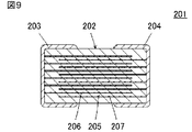
- FIG. 9 shows a cross-sectional view of the multilayer ceramic capacitor 201.
- the multilayer ceramic capacitor 201 includes a ceramic multilayer body 202 and a first external electrode 203 and a second external electrode 204 provided on the surface of the ceramic multilayer body 202.
- the ceramic laminate 202 is a laminate in which capacitor elements each having a ceramic dielectric layer 205 inserted between a first internal electrode 206 and a second internal electrode 207 are connected in parallel.
- Such a multilayer ceramic capacitor 201 is excellent in reliability and durability, and can realize a small size and a large capacity.
- the small-sized and large-capacity monolithic ceramic capacitor 201 often uses a high dielectric constant ceramic material based on barium titanate as the material of the ceramic dielectric layer 205 constituting the ceramic laminate 202.
- a voltage is applied to the multilayer ceramic capacitor 201 including such a ceramic multilayer body 202, a distortion corresponding to the magnitude of the applied voltage is generated in the ceramic multilayer body 202 due to the electrostrictive effect and the inverse piezoelectric effect.
- the ceramic laminate 202 repeatedly expands in the stacking direction and contracts in the plane direction orthogonal to the stacking direction.
- Such vibration of the substrate B may cause malfunction of the acceleration sensor when an acceleration sensor such as a shock sensor is mounted on the substrate B.
- both the solder S and the embedded layer cause the distortion of the ceramic multilayer body 202 to the substrate. It is possible to transmit to B. In that case, there is a concern that the vibration of the substrate B described above becomes large and the audible sound becomes large.
- an object of the present invention is to reduce vibration even if distortion due to application of voltage occurs in an electronic component embedded in an embedded layer including a resin material portion, and further prevent or reduce generation of audible sound due to vibration.
- An electronic component built-in substrate and a manufacturing method thereof are provided.
- the embedded component is reduced in order to reduce vibration of the electronic component built-in substrate and to prevent or reduce generation of audible sound due to vibration. Improvements in layer thickness are achieved.
- An electronic component built-in substrate includes a core substrate having one parallel main surface and the other main surface, at least one electronic component mounted on one main surface of the core substrate, and an embedded layer. .
- the electronic component is a multilayer capacitor including a multilayer body, and a first external electrode and a second external electrode provided on the surface of the multilayer body.
- the multilayer body includes a capacitance developing portion in which a capacitor element in which a dielectric layer is inserted between a first internal electrode and a second internal electrode is stacked, and a first sandwiching the capacitance developing portion.
- the protection part and the second protection part are included.
- the first external electrode is connected to the first internal electrode.
- the second external electrode is connected to the second internal electrode.
- the material of the dielectric in the multilayer capacitor is not particularly limited as long as it can be distorted by applying a voltage.
- the embedded layer is provided so that an electronic component is embedded in one main surface of the core substrate and the outer surface is parallel to the one main surface of the core substrate.
- the buried layer thickness T R the buried layer elastic modulus E R , the core substrate thickness T B , the core substrate elastic modulus E B, and the static when the one principal surface of the core substrate is the reference plane.
- the height T C of the center of the capacity expression unit thereby satisfying the expression (1).
- the buried layer thickness T R In the electronic component built-in substrate, the buried layer thickness T R , the buried layer elastic modulus E R , the core substrate thickness T B , the core substrate elastic modulus E B, and the center of the capacitance developing portion
- the height T C satisfies the relationship represented by the formula (1).
- the electronic component built-in substrate includes a core substrate, a first portion of an embedded layer having a thickness T C above and below the center of the electrostatic capacity developing portion of the electronic component, and an embedded portion obtained by subtracting the first portion from the thickness of the entire embedded layer.
- the first portion of the embedded layer is substantially symmetrical on the top and bottom of the center surface of the capacitance developing portion, and even if distortion occurs in the electronic component, It is considered that the layer and the lower layer vibrate so as to cancel each other's vibrations.
- the relationship represented by the above formula (1) is that the core substrate and the second portion of the buried layer include the interaction with the first portion of the buried layer, as seen from the center plane of the capacitance developing portion. It is inferred that it represents a condition that vibrates so as to cancel each other's vibrations.
- each component in the electronic component built-in substrate satisfies the relationship expressed by the expression (1), thereby reducing vibration of the electronic component built-in substrate and preventing or reducing generation of audible sound due to vibration. it can.
- the first preferred embodiment of the electronic component built-in substrate according to the present invention includes a buried layer thickness T R , a buried layer elastic modulus E R , a core substrate thickness T B, and a core substrate elastic modulus E B.
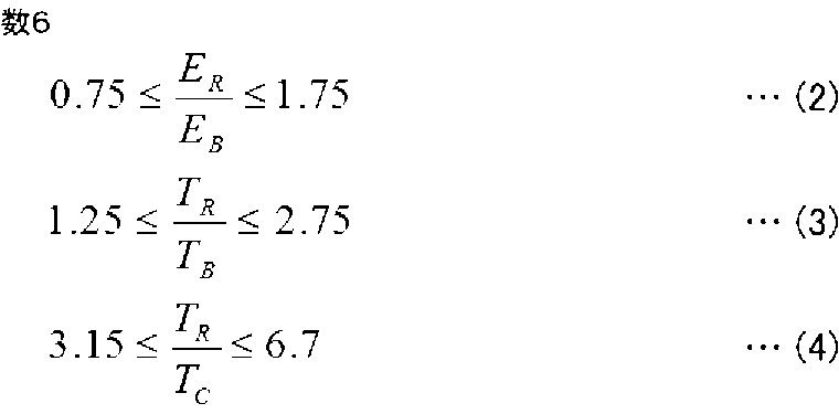
- the buried layer thickness T R the buried layer elastic modulus E R , the core substrate thickness T B , the core substrate elastic modulus E B, and the center of the capacitance developing portion and height T C is, which satisfies the relationship represented by equation (1) to (4) below.
- each component in the electronic component built-in substrate as represented by the above formulas (2) to (4), the above-mentioned core substrate and the second portion of the buried layer are connected to the first portion of the buried layer. It is inferred that they vibrate so as to surely cancel each other's vibrations, as seen from the center plane of the capacitance developing part, including the interaction with the.
- the thickness of the first protective part of the electronic component is thicker than the thickness of the second protective part. Furthermore, the electronic component is mounted such that the first protection portion is on the one main surface side of the core substrate.
- the center of the electrostatic capacity developing portion of the electronic component is more from one main surface of the core substrate than when the first protective portion and the second protective portion have the same thickness. It is in a high position.
- the dimensions of each component in the electronic component built-in substrate satisfy the relationship between the above-described embodiment and the first preferred embodiment, and thus the electronic component built-in substrate has already been reduced to some extent even when there is no embedded layer. Vibration can be further reduced, and generation of audible sound due to vibration can be more reliably prevented or reduced.
- the present invention is also directed to a method for manufacturing an electronic component built-in substrate.
- a method of manufacturing an electronic component built-in substrate according to the present invention includes a core substrate having one parallel main surface and the other main surface, at least one electronic component mounted on one main surface of the core substrate, an embedded layer, The manufacturing method of the electronic component built-in board
- the electronic component is a multilayer capacitor including a multilayer body, and a first external electrode and a second external electrode provided on the surface of the multilayer body.
- the multilayer body includes a capacitance developing portion in which a capacitor element in which a dielectric layer is inserted between a first internal electrode and a second internal electrode is stacked, and a first sandwiching the capacitance developing portion.
- the protection part and the second protection part are included.
- the first external electrode is connected to the first internal electrode.
- the second external electrode is connected to the second internal electrode.
- the embedded layer is provided so that an electronic component is embedded in one main surface of the core substrate and the outer surface is parallel to the one main surface of the core substrate.
- the method for manufacturing an electronic component built-in substrate according to the present invention includes a mounting step and a buried layer forming step.
- the mounting process is a process of mounting an electronic component on one main surface of the core substrate.
- the buried layer forming step is a step of providing a buried layer for embedding the electronic component on one main surface of the core substrate.
- the buried layer R includes the thickness T R of the buried layer, the elastic modulus E R of the buried layer, the thickness T B of the core substrate, the elastic modulus E B of the core substrate, and one of the core substrates. and height T C of the center of the electrostatic capacity developing unit upon a reference plane surface is provided so as to satisfy the expression (1).
- the embedded layer is formed so that each component in the electronic component built-in substrate satisfies the relationship represented by the formula (1).
- a first preferred embodiment of the method of manufacturing an electronic component-embedded substrate according to the present invention the buried layer forming step, the buried layer R has a thickness T R of the buried layer, and the elastic modulus E R of the buried layer, the core substrate
- the thickness T B of the core substrate, the elastic modulus E B of the core substrate, and the center height T C of the capacitance developing portion when one main surface of the core substrate is used as a reference surface are expressed by the above equation (1).
- it is provided so as to further satisfy the expressions (2) to (4).
- the embedded layer is formed so that each component in the electronic component built-in substrate satisfies the relationship expressed by the equations (1) to (4). .
- the buried layer thickness T R the buried layer elastic modulus E R , the core substrate thickness T B , the core substrate elastic modulus E B, and the capacitance developing portion
- the center height T C satisfies the relationship expressed by the above formula (1).
- the embedded layer is formed so that each component in the electronic component built-in substrate satisfies the relationship represented by the above formula (1). To do.
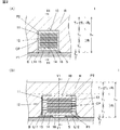
- FIG. 1 is a top view of an electronic component built-in substrate 1 according to an embodiment of the present invention.
- 1 is a cross-sectional view of an electronic component built-in substrate 1 according to an embodiment of the present invention.
- FIG. 2A is a cross-sectional view taken along the line Y1-Y1 in FIG.
- FIG. 2B is a cross-sectional view taken along the line X1-X1 in FIG.
- It is an external appearance perspective view for demonstrating the deflection amount h when the external force F acts on plate-shaped member PM.
- It is a graph which shows the result of having calculated
- FIG. 1 is a top view of an electronic component built-in substrate 1 according to an embodiment of the present invention.
- FIG. 2A is a cross-sectional view taken along the line Y1-Y1 in FIG. 2B is a cross-sectional view taken along the line X1-X1 in FIG.
- the electronic component built-in substrate 1 includes a core substrate B, an electronic component 10, and an embedded layer R.
- the electronic component 10 is mounted on one main surface of the core substrate B having one main surface and the other main surface that are parallel in the error range.
- the embedded layer R is provided so that the electronic component 10 is embedded in one main surface of the core substrate B, and the outer surface is parallel to the one main surface of the core substrate B in an error range.
- the buried layer R includes a resin material portion.
- the resin material portion is formed using a resin material in which a glass material, silica, or the like is dispersed as a filler.
- the buried layer R may further include a conductive material part provided on the surface of the resin material part in addition to the resin material part (not shown in FIGS. 1 and 2).
- the core substrate B is a multilayer substrate corresponding to the above-described FIG. 6, and is illustrated in a simplified manner with internal electrodes and vias not shown.
- the size relationship between the core substrate B and the electronic component 10 is different from the actual one.
- the electronic component 10 is a multilayer ceramic capacitor including a ceramic multilayer body 11, a first external electrode 12, and a second external electrode 13.
- the ceramic multilayer body 11 includes a capacitance developing portion CP in which a capacitor element in which a ceramic dielectric layer 14 is inserted between a first internal electrode 15 and a second internal electrode 16 is laminated. The structure is sandwiched between the ceramic protection part P1 and the second ceramic protection part P2.
- the ceramic laminate 11 has two end faces facing each other and a side face connecting the two end faces.
- the first external electrode 12 is connected to the first internal electrode 15, and the second external electrode 13 is connected to the second internal electrode 16.
- the first external electrode 12 and the second external electrode 13 are each provided on the surface of the ceramic laminate 11.
- the dielectric material may be a ceramic material as long as it can be distorted by voltage application.
- the present invention can also be applied to a multilayer metallized film capacitor which is a multilayer capacitor using a resin material as a dielectric material other than a ceramic material.
- the electronic component 10 is mounted on the mounting lands L11 and L12 using the solder S.
- the material of the mounting lands L11 and L12 and the material of the solder S can be appropriately selected from existing ones.
- the mounting lands L11 and L12 are on a wiring including a conductive pattern (not shown). A voltage is applied to the electronic component 10 through this wiring.
- the electronic component built-in substrate 1 may have a plurality of electronic components 10 mounted thereon. Similarly, electronic components other than the multilayer ceramic capacitor may be mounted on the electronic component built-in substrate 1.
- the electronic component 10 which is a multilayer ceramic capacitor is often made of a high dielectric constant ceramic material based on barium titanate, it may vibrate due to distortion during voltage application. This vibration is transmitted to the substrate B fixed to the electronic component 10 through the solder S. When the electronic component 10 is embedded in the embedded layer R, the substrate B is also transmitted through the embedded layer R. Is transmitted to.
- Buried layer R has a thickness T R of the buried layer, and the elastic modulus E R of the buried layer, the thickness T B of the core substrate, and the elastic modulus E B of the core substrate, and the reference plane of the one main surface of the core board B
- the height T C of the center of the capacitance developing portion satisfies the expression (1), and preferably satisfies the expressions (2) to (4).
- the electronic component built-in substrate 1 includes the core substrate B, the first portion R 1 of the embedded layer having a thickness T C above and below the center of the electrostatic capacity developing portion CP of the electronic component 10, and the embedded layer. It is configured to include three parts, a second part R 2 of the buried layer obtained by subtracting the first part from the entire thickness.
- the first portion R 1 includes the mounting lands L11 and L12 and the solder S, precisely, the top and bottom thereof are symmetrical with respect to the center plane of the electrostatic capacitance developing portion CP of the electronic component 10. Absent. However, the mounting lands L11 and L12 and the solder S are thinner than the thickness of the buried layer R, and can be ignored in order to simplify the structure.
- the upper layer and the lower layer on the center plane of the capacitance developing portion CP are substantially symmetric. In that case, even if distortion occurs due to the application of voltage to the electronic component 10 in the first portion R 1 , the upper layer and the lower layer on the center plane of the capacitance developing part CP mutually vibrate. Will vibrate so as to cancel each other.
- the second portion R 2 of the embedded layer and the core substrate B cancel each other's vibration when viewed from the center plane of the capacitance developing portion CP. It only has to vibrate to fit.
- a single plate-like member PM having a distance L, a width W, a thickness T, and an elastic modulus E between fulcrums as shown in FIG. 3A is caused by the action of an external force F as shown in FIG.
- the deflection amount h is expressed by equation (5).
- Equation (7) indicates that when the deflection of the core substrate B and the second portion R 2 of the buried layer is the same size and in the opposite direction, that is, the core substrate B and the second portion R 2 of the buried layer are It represents the case of vibrating so as to cancel out the vibrations.
- the second portion R 2 and the upper layer of the first portion R 1 influence each other due to factors that are not taken into account when vibrating.
- the core substrate B and the lower layer of the first portion R1 influence each other due to factors that are not taken into account when vibrating. For this reason, the second portion R 2 and the core substrate B cannot be handled as being individually vibrated.
- the thickness T R of the buried layer and the thickness T B of the core substrate are variables, and the ratio E B / B between the elastic modulus E B of the core substrate and the elastic modulus E R of the buried layer.
- a linear equation was assumed in which E R and the center height T C of the capacitance developing portion were constant.
- the actual vibration is obtained using the exponent m of the ratio E B / E R of the elastic modulus E B of the core substrate and the elastic modulus E R of the buried layer as a fitting parameter. Based on the state, a vibration conditional expression was obtained. That is, the above linear equation is expressed by equation (8).
- the vibration parameter VP indicating the vibration of the electronic component built-in substrate 1 is expressed by the equation (9) obtained by dividing the right side of the equation (8) by the elastic modulus E R of the buried layer.
- the vibration parameter VP When the vibration parameter VP is 1, the vibration of the electronic component built-in substrate 1 is the smallest. On the other hand, as the vibration parameter VP is further away from 1, the vibration of the electronic component built-in substrate 1 increases.
- the present inventor has found that by controlling the vibration parameter VP, it is possible to control the vibration of the electronic component built-in substrate and the generation of an audible sound based on the vibration, thereby achieving the present invention.
- the magnitude of the sound pressure corresponding to the vibration of the substrate in the state where the electronic component 10 is not embedded in the embedded layer R is set as the reference sound pressure, and the range of the vibration parameter VP corresponding to the range smaller than the reference sound pressure.
- the sound pressure is a value obtained by converting the largest amplitude among vibrations generated in the audible range into a loudness.
- the inventor of the present invention has defined an upper limit value A and a lower limit value B of the vibration parameter VP that is smaller than the reference sound pressure, and a power exponent m value based on the above technical idea.
- the thickness T R of the electronic component built-buried layer provided on the major surface one substrate 1 the relationship between the sound pressure corresponding to the magnitude of the vibration, based on the finite element method for elastic modulus E R of various buried layer Obtained by simulation. Then, by comparing with the simulation result, the upper limit value A and the lower limit value B of the vibration parameter VP and the power exponent m were determined.
- the thickness T R of the electronic components provided on one main surface of the built-in substrate 1 buried layer the relationship between the sound pressure corresponding to the magnitude of the vibration, the results obtained by simulation based on the finite element method It is a graph to show.
- the sound pressure represents the magnitude of a sound (so-called “squeal”) generated in the L direction of the electronic component 10 (a direction parallel to the core substrate B in FIG. 2B).
- squeal a sound generated in the L direction of the electronic component 10 (a direction parallel to the core substrate B in FIG. 2B).
- the electronic component 10 is mounted such that the internal electrodes 15 and 16 are parallel to the core substrate B.
- the thickness T B of the core substrate is 0.8 mm
- the elastic modulus E B of the core substrate is 20 GPa
- the center height T C of the capacitance developing portion is 0.315 mm.
- Modulus E B of the core substrate B uses a value plausible as the elastic modulus generally glass epoxy substrate used (flexural modulus).
- Electronic component 10 as the length of the L direction is embedded in the buried layer R of 24 mm, and calculating the change in sound pressure due to the change of the thickness T R of the buried layer.
- FIG. 4 shows three simulation results when the elastic modulus E R of the buried layer is 15 GPa, 25 GPa, and 35 GPa.
- the thickness T R was focused on.
- the thickness T R of the buried layer at which the sound pressure is a minimum value is about 1.6 mm, about 1.3 mm, and about 1.15 mm, respectively.
- the exponent m is 3/4
- the upper limit value A of the vibration parameter VP is 1.2
- the lower limit value B is 0.8. I understood.
- the thickness T R of the buried layer, and the elastic modulus E R of the buried layer, the thickness T B of the core substrate, and the elastic modulus E B of the core substrate, when a reference plane one major surface of the core board B When the relationship with the center height T C of the electrostatic capacity developing portion satisfies the expression (1), vibration of the electronic component built-in substrate 1 is reduced, and generation of audible sound due to vibration is prevented or reduced. The Therefore, the sound pressure of the audible sound due to the vibration of the electronic component built-in substrate 1 becomes smaller than the reference sound pressure.
- FIG. 5 is a cross-sectional view of Modification 1A of the electronic component built-in substrate according to the embodiment of the present invention.
- FIG. 5A corresponds to an arrow cross-sectional view (FIG. 2A) of a plane including a Y1-Y1 line in FIG.
- FIG. 5B corresponds to an arrow cross-sectional view (FIG. 2B) of the plane including the line X1-X1 in FIG.
- the thickness of the first ceramic protection portion P1 of the electronic component 10 is larger than the thickness of the second ceramic protection portion P2. Further, the electronic component 10 is mounted such that the first ceramic protection portion P1 is on the one main surface side of the core substrate B.
- the core substrate B is illustrated in a simplified manner as in the above-described embodiment.
- the center of the electrostatic capacity developing portion CP of the electronic component 10 is the same thickness as the first ceramic protective portion P1 and the second ceramic protective portion P2. Compared with the case where it has, it is a higher position from the one main surface of the core substrate B.
- Japanese Patent Laid-Open No. 2013-65820 describes that vibration of an electronic component built-in substrate can be effectively reduced by mounting the electronic component 10 having the above structure on a core substrate B.
- FIGS. 6 and 7 are diagrams schematically showing a mounting process and a buried layer forming process sequentially performed in the example of the method for manufacturing the electronic component built-in substrate 1.
- FIGS. 6 and 7 corresponds to an arrow sectional view (FIG. 2A) of a plane including the Y1-Y1 line of FIG.
- ⁇ Mounting process> 6A and 6B are diagrams schematically showing a mounting process of the method for manufacturing the electronic component built-in substrate 1. Through the mounting process, the electronic component 10 is mounted on one main surface of the core substrate B.
- FIG. 6A shows a stage of preparing the electronic component 10 and the core substrate B on which the electronic component 10 is mounted.
- the electronic component 10 is a multilayer ceramic capacitor having the above-described structure and generating distortion when a voltage is applied.
- the core substrate 10 includes mounting lands L11 and L12 (L12 not shown) for joining the electronic component 10 on one main surface.
- FIG. 6B shows a stage in which the electronic component 10 is mounted on one main surface of the core substrate 10 by joining the mounting lands L11 and L12 using the solder S.
- the center plane of the capacitance developing part CP has a height T C when one main surface of the core substrate B is used as a reference plane.
- ⁇ Embedded layer formation process> 7A and 7B are diagrams schematically showing a buried layer forming step of the method for manufacturing the electronic component built-in substrate 1.
- the embedded layer R is provided on one main surface of the core substrate B so that the electronic component 10 is embedded.
- FIG. 7A shows a step of applying a liquid resin LR to one main surface of the core substrate B on which the electronic component 10 is mounted, for example, with a dispenser D so as to have a predetermined thickness represented by a one-dot chain line. Indicates.
- the apparatus used for coating is not limited to the dispenser D described above, and an existing coating apparatus can be used.
- various coaters such as a curtain coater and a spin coater may be used.
- liquid resin LR is not limited to a single resin material, and a resin material containing a filler such as a glass material or silica as a filler can be used.
- the embedded layer R is not limited to the method of applying the liquid resin LR as shown in FIG. 7A, but a sheet-like prepreg is placed on one main surface of the core substrate B in a semi-cured state, and an electronic component You may form by pressing so that 10 may be embedded.
- FIG. 7B shows a stage in which the liquid resin LR in which the electronic component 10 is embedded is heated and cured to obtain a buried layer R after curing.
- the embedded layer R after curing has its thickness T R , the elastic modulus E R of the embedded layer, the thickness T B of the core substrate, the elastic modulus E B of the core substrate, and the center of the capacitance developing portion. of the height T C is formed so as to satisfy the expression (1).
- the relationship represented by the above formula (1) is that the core substrate B and the second portion R 2 of the buried layer include the interaction between the first portion R 1 of the buried layer and the electrostatic capacitance.
- the core substrate B and the second portion R 2 of the buried layer include the interaction between the first portion R 1 of the buried layer and the electrostatic capacitance.
- the embedded layer R is formed so that each component in the electronic component built-in substrate 1 satisfies the relationship represented by the expression (1), so that the vibration in the audible frequency range described above is generated.
- An electronic component-embedded substrate that is smaller and reliably prevents or reduces the generation of audible sound can be efficiently manufactured.
- the embedded layer R is provided so that each component in the electronic component built-in substrate 1 further satisfies the expressions (2) to (4) in addition to the above expression (1). It is preferred that
- the embedded layer forming step by forming the embedded layer R so that each component in the electronic component built-in substrate 1 satisfies the relationship expressed by the formulas (1) to (4), the above-mentioned audible frequency range is obtained. Therefore, it is possible to efficiently manufacture an electronic component built-in substrate in which the vibration of the electronic component is smaller and the generation of audible sound is reliably prevented or reduced.
- Adjustment of the thickness T R of the buried layer, in anticipation of volume change upon curing of the resin LR liquid, after curing the resin LR liquid may be applied to a thickness of T R. Further, the resin LR liquid was coated in advance larger amount, by removing the excess resin after curing, the thickness T R of the buried layer may be a desired value.
- substrate 10 Electronic component (multilayer ceramic capacitor), 11 Ceramic laminated body, 12 1st external electrode, 13 2nd external electrode, 14 Ceramic dielectric layer, 15 1st internal electrode, 16 2nd internal electrodes, B core substrate, CP capacitance expression of, P1 first ceramic protective part, P2 second ceramic protective part, R buried layer, T C capacitance expression unit center height, T B the thickness of the core substrate, the elastic modulus of E B core substrate, the thickness of T R buried layer, the elastic modulus of E R buried layer.
Landscapes
- Engineering & Computer Science (AREA)
- Manufacturing & Machinery (AREA)
- Microelectronics & Electronic Packaging (AREA)
- Production Of Multi-Layered Print Wiring Board (AREA)
Abstract
電子部品内蔵基板(1)は、コア基板(B)と、コア基板(B)の一方主面に実装された電子部品(10)と、電子部品(10)を埋設して設けられた埋設層(R)とを備える。電子部品(10)は、セラミック積層体(11)を備える積層セラミックコンデンサである。セラミック積層体(11)は、セラミック誘電体層(14)が第1の内部電極(15)と第2の内部電極(16)との間に挿入されてなるコンデンサ素子が積層された静電容量発現部(CP)を含む。埋設層(R)の厚み(TR)と、埋設層(R)の弾性率(ER)と、コア基板(B)の厚み(TB)と、コア基板(B)の弾性率(EB)と、コア基板(B)の一方主面を基準面としたときの静電容量発現部(CP)の中心の高さ(TC)とは、【数1】を満足する。
Description
この発明は、コア基板と、コア基板の一方主面に実装された電子部品と、その電子部品を埋設して設けられた埋設層とを備える電子部品内蔵基板、およびその製造方法に関するものである。
近年、携帯型電子機器の薄型化を受けて、国際公開第2011/135926号(特許文献1)のように、基板内部に電子部品を埋設することにより基板の薄型化を図った電子部品内蔵基板が提案されている。
図8は、特許文献1に記載されている電子部品内蔵基板100の断面図である。図8に記載の電子部品内蔵基板100では、コア基板108に電子部品101、102が実装され、それらの電子部品101、102が埋設されるように埋設層109が形成されている。
このような電子部品内蔵基板100は、軽量であり、かつセラミック基板のように高温焼成を伴わないため、内蔵する電子部品に制約が少ないという利点がある。
ここで、特許文献1に記載の電子部品内蔵基板100の埋設層109に埋設される電子部品101、102として、積層セラミックコンデンサを考える。図9に、積層セラミックコンデンサ201の断面図を示す。
積層セラミックコンデンサ201は、セラミック積層体202と、セラミック積層体202の表面に設けられる第1の外部電極203および第2の外部電極204とを備える。セラミック積層体202は、セラミック誘電体層205が第1の内部電極206と第2の内部電極207との間に挿入されてなるコンデンサ素子が、並列接続されて積層されたものである。そのような積層セラミックコンデンサ201は、信頼性および耐久性に優れ、小型大容量を実現することができる。
小型大容量の積層セラミックコンデンサ201は、セラミック積層体202を構成するセラミック誘電体層205の材料として、チタン酸バリウムを基本材料とする高誘電率のセラミック材料を用いることが多い。そのようなセラミック積層体202を備える積層セラミックコンデンサ201に電圧を印加すると、電歪効果および逆圧電効果により、印加された電圧の大きさに応じた歪みがセラミック積層体202に発生する。それに伴い、セラミック積層体202が、積層方向への膨張、積層方向と直交する面方向への収縮を繰り返す。
近年、積層セラミックコンデンサ201の小型化・薄層化の進展に伴い、誘電体に印加される電界強度が高くなったため、上記のセラミック積層体202の歪みの度合いも大きくなっている。
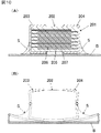
ここで、図10(A)に示すように、積層セラミックコンデンサ201が、はんだSにより基板Bに実装された場合を考える。積層セラミックコンデンサ201に電圧が印加されると、図10(B)に示すように、セラミック積層体202に発生した歪みが、はんだSを介して積層セラミックコンデンサ201に固着されている基板Bを振動させる。
このような基板Bの振動は、基板Bに例えばショックセンサなどの加速度センサが実装されていた場合、加速度センサの誤作動を引き起こす可能性がある。
また、その振動数が可聴域である20Hz~20kHzである場合、可聴音として人間の耳に認識される。この現象は「鳴き(acoustic noise)」とも言われ、電子機器の静寂化に伴い、ノートパソコン、携帯電話、デジタルカメラなどの様々なアプリケーションの電源回路などにおける設計の課題となっている。
積層セラミックコンデンサ201を上記のように基板BにはんだSにより実装し、さらに特許文献1に記載のように埋設層に埋設した場合、はんだSと埋設層とが共にセラミック積層体202の歪みを基板Bに伝達することが考えられる。その場合、前述の基板Bの振動が大きくなり、また可聴音が大きくなることが懸念される。
そこで、この発明の目的は、樹脂材料部を含む埋設層に埋設されている電子部品に電圧の印加による歪みが発生したとしても、振動が低減され、さらに振動による可聴音の発生が防止または低減された電子部品内蔵基板、およびその製造方法を提供することである。
この発明では、埋設層に埋設されている電子部品に電圧の印加による歪みが発生したとしても、電子部品内蔵基板の振動を低減し、さらに振動による可聴音の発生を防止または低減するため、埋設層の厚みについての改良が図られる。
この発明は、まず電子部品内蔵基板に向けられる。
この発明に係る電子部品内蔵基板は、平行な一方主面と他方主面とを有するコア基板と、コア基板の一方主面に実装された、少なくとも1つの電子部品と、埋設層と、を備える。
この発明に係る電子部品内蔵基板は、平行な一方主面と他方主面とを有するコア基板と、コア基板の一方主面に実装された、少なくとも1つの電子部品と、埋設層と、を備える。
上記の電子部品は、積層体と、積層体の表面に設けられる第1の外部電極および第2の外部電極と、を備える積層コンデンサである。
積層体は、誘電体層が第1の内部電極と第2の内部電極との間に挿入されてなるコンデンサ素子が積層された静電容量発現部と、その静電容量発現部を挟む第1の保護部および第2の保護部とを含む。第1の外部電極は、第1の内部電極と接続される。第2の外部電極は、第2の内部電極と接続される。
なお、上記の積層コンデンサにおける誘電体の材質は、電圧の印加により歪みが発生し得るものであれば特に問わない。
上記の埋設層は、コア基板の一方主面に、電子部品を埋設し、かつ外表面が前記コア基板の一方主面と平行となるように設けられている。
そして、埋設層の厚みTRと、埋設層の弾性率ERと、コア基板の厚みTBと、コア基板の弾性率EBと、コア基板の一方主面を基準面としたときの静電容量発現部の中心の高さTCとは、(1)式を満足する。

上記の電子部品内蔵基板では、埋設層の厚みTRと、埋設層の弾性率ERと、コア基板の厚みTBと、コア基板の弾性率EBと、静電容量発現部の中心の高さTCとが、(1)式で表される関係を満足している。
電子部品内蔵基板は、コア基板と、電子部品の静電容量発現部の中心から上下にそれぞれ厚みTCを有する埋設層の第1部分と、埋設層全体の厚みから第1部分を差し引いた埋設層の第2部分と、の3つの部分を含んで構成される。
ここで、埋設層の第1部分は、静電容量発現部の中心面の上下が実質的に対称であり、電子部品に歪みが発生したとしても、静電容量発現部の中心面の上側の層と下側の層とは、互いの振動を打ち消し合うように振動すると考えられる。
上記の(1)式で表される関係は、コア基板と埋設層の第2部分とが、埋設層の第1部分との相互作用を含め、静電容量発現部の中心面から見て、互いの振動を打ち消し合うように振動する条件を表していると推察される。
したがって、電子部品内蔵基板における各構成要素が(1)式で表される関係を満足することにより、電子部品内蔵基板の振動を低減し、さらに振動による可聴音の発生を防止または低減することができる。
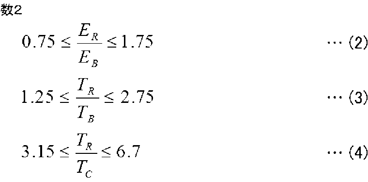
この発明に係る電子部品内蔵基板における第1の好ましい実施形態は、埋設層の厚みTRと、埋設層の弾性率ERと、コア基板の厚みTBと、コア基板の弾性率EBと、コア基板の一方主面を基準面としたときの静電容量発現部の中心の高さTCとが、上記の(1)式に加えて、(2)式~(4)式をさらに満足する。

上記の電子部品内蔵基板では、埋設層の厚みTRと、埋設層の弾性率ERと、コア基板の厚みTBと、コア基板の弾性率EBと、静電容量発現部の中心の高さTCとが、(1)式~(4)式で表される関係を満足している。
電子部品内蔵基板における各構成要素を上記の(2)式~(4)式で表されるように定めることにより、前述のコア基板と埋設層の第2部分とが、埋設層の第1部分との相互作用を含め、静電容量発現部の中心面から見て、互いの振動を確実に打ち消し合うように振動すると推察される。
したがって、電子部品内蔵基板における各構成要素が(1)式~(4)式で表される関係を満足することにより、電子部品内蔵基板の振動を確実に低減し、さらに振動による可聴音の発生を確実に防止または低減することができる。
この発明に係る電子部品内蔵基板における第2の好ましい実施形態は、電子部品の第1の保護部の厚みが、第2の保護部の厚みより厚くなっている。さらに、電子部品は、第1の保護部がコア基板の一方主面側となるように実装されている。
上記の電子部品内蔵基板では、電子部品の静電容量発現部の中心が、第1の保護部と第2の保護部とが同じ厚みを有する場合と比べて、コア基板の一方主面からより高い位置となっている。
上記の構造を有する電子部品をコア基板に実装することにより、効果的に電子部品内蔵基板の振動を低減できることが、別途確認されている。
したがって、電子部品内蔵基板における各構成要素の寸法が前述の実施形態および第1の好ましい実施形態の関係を満足することにより、埋設層がない場合でも、既にある程度まで低減されている電子部品内蔵基板の振動をさらに低減させ、振動による可聴音の発生をさらに確実に防止または低減することができる。
また、この発明は、電子部品内蔵基板の製造方法にも向けられる。
この発明に係る電子部品内蔵基板の製造方法は、平行な一方主面と他方主面とを有するコア基板と、コア基板の一方主面に実装された、少なくとも1つの電子部品と、埋設層と、を備える電子部品内蔵基板の製造方法である。
この発明に係る電子部品内蔵基板の製造方法は、平行な一方主面と他方主面とを有するコア基板と、コア基板の一方主面に実装された、少なくとも1つの電子部品と、埋設層と、を備える電子部品内蔵基板の製造方法である。
上記の電子部品は、積層体と、積層体の表面に設けられる第1の外部電極および第2の外部電極と、を備える積層コンデンサである。
積層体は、誘電体層が第1の内部電極と第2の内部電極との間に挿入されてなるコンデンサ素子が積層された静電容量発現部と、その静電容量発現部を挟む第1の保護部および第2の保護部とを含む。第1の外部電極は、第1の内部電極と接続される。第2の外部電極は、第2の内部電極と接続される。
上記の埋設層は、コア基板の一方主面に、電子部品を埋設し、かつ外表面が前記コア基板の一方主面と平行となるように設けられている。
この発明に係る電子部品内蔵基板の製造方法は、実装工程と、埋設層形成工程と、を備える。
実装工程は、コア基板の一方主面に、電子部品を実装する工程である。
埋設層形成工程は、コア基板の一方主面に、電子部品を埋設する埋設層を設ける工程である。埋設層形成工程において、埋設層Rは、埋設層の厚みTRと、埋設層の弾性率ERと、コア基板の厚みTBと、コア基板の弾性率EBと、コア基板の一方主面を基準面としたときの静電容量発現部の中心の高さTCとが、(1)式を満足するように設けられる。
埋設層形成工程は、コア基板の一方主面に、電子部品を埋設する埋設層を設ける工程である。埋設層形成工程において、埋設層Rは、埋設層の厚みTRと、埋設層の弾性率ERと、コア基板の厚みTBと、コア基板の弾性率EBと、コア基板の一方主面を基準面としたときの静電容量発現部の中心の高さTCとが、(1)式を満足するように設けられる。

上記の電子部品内蔵基板の製造方法では、埋設層形成工程において、電子部品内蔵基板における各構成要素が(1)式で表される関係を満足するように埋設層を形成する。
したがって、前述の可聴周波数域内での振動が小さく、可聴音の発生が防止または低減された電子部品内蔵基板を、効率的に製造することができる。
この発明に係る電子部品内蔵基板の製造方法における第1の好ましい実施形態は、埋設層形成工程において、埋設層Rは、埋設層の厚みTRと、埋設層の弾性率ERと、コア基板の厚みTBと、コア基板の弾性率EBと、コア基板の一方主面を基準面としたときの静電容量発現部の中心の高さTCとが、上記の(1)式に加えて、(2)式~(4)式をさらに満足するように設けられる。
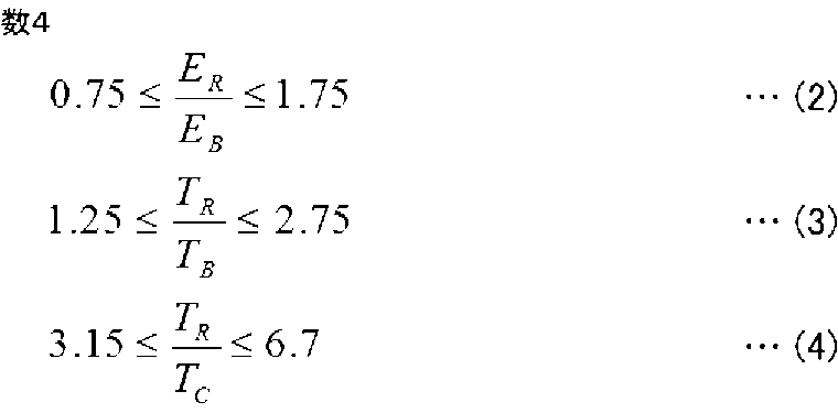
上記の電子部品内蔵基板の製造方法では、埋設層形成工程において、電子部品内蔵基板における各構成要素が(1)式~(4)式で表される関係を満足するように埋設層を形成する。
したがって、前述の可聴周波数域内での振動がより小さく、可聴音の発生が確実に防止または低減された電子部品内蔵基板を、効率的に製造することができる。
この発明に係る電子部品内蔵基板では、埋設層の厚みTRと、埋設層の弾性率ERと、コア基板の厚みTBと、コア基板の弾性率EBと、静電容量発現部の中心の高さTCとが、上記の(1)式で表される関係を満足している。
したがって、埋設層に埋設されている電子部品に電圧の印加による歪みが発生したとしても、電子部品内蔵基板の振動を低減し、さらに振動による可聴音の発生を防止または低減することができる。
また、この発明に係る電子部品内蔵基板の製造方法では、埋設層形成工程において、電子部品内蔵基板における各構成要素が上記の(1)式で表される関係を満足するように埋設層を形成する。
したがって、前述の可聴周波数域内での振動が小さく、可聴音の発生が防止または低減された電子部品内蔵基板を、効率的に製造することができる。
以下にこの発明の実施形態を示して、本発明の特徴とするところをさらに詳しく説明する。
-電子部品内蔵基板の実施形態-
この発明の実施形態に係る電子部品内蔵基板1について、図1および図2を用いて説明する。
この発明の実施形態に係る電子部品内蔵基板1について、図1および図2を用いて説明する。
<電子部品内蔵基板の構造>
図1は、この発明の実施形態に係る電子部品内蔵基板1の上面図である。図2(A)は図1のY1-Y1線を含む面の矢視断面図である。図2(B)は図1のX1-X1線を含む面の矢視断面図である。
図1は、この発明の実施形態に係る電子部品内蔵基板1の上面図である。図2(A)は図1のY1-Y1線を含む面の矢視断面図である。図2(B)は図1のX1-X1線を含む面の矢視断面図である。
この発明の実施形態に係る電子部品内蔵基板1は、コア基板Bと、電子部品10と、埋設層Rとを備える。電子部品10は、誤差範囲において平行な一方主面と他方主面とを有するコア基板Bの一方主面に実装されている。埋設層Rは、コア基板Bの一方主面に、電子部品10を埋設し、かつ外表面がコア基板Bの一方主面と誤差範囲において平行となるように設けられている。
この発明の実施形態に係る電子部品内蔵基板1において、埋設層Rは樹脂材料部を含む。樹脂材料部は、後述するようにフィラーとしてガラス材料やシリカなどを分散させた樹脂材料を用いて形成される。なお、埋設層Rは、樹脂材料部に加えて、樹脂材料部の表面に設けられた導電材料部をさらに含んでいてもよい(図1および図2では不図示)。
なお、コア基板Bは、前述の図6に相当する多層基板であり、内部電極やビアなどを不図示として、簡略化して図示されている。また、この発明の実施形態では、電子部品10を強調するため、コア基板Bと、電子部品10との大きさの関係は、実際のものとは異なっている。
電子部品10は、セラミック積層体11と、第1の外部電極12および第2の外部電極13とを備える積層セラミックコンデンサである。セラミック積層体11は、セラミック誘電体層14が第1の内部電極15と第2の内部電極16との間に挿入されてなるコンデンサ素子が積層された静電容量発現部CPが、第1のセラミック保護部P1および第2のセラミック保護部P2で挟まれた構造となっている。
セラミック積層体11は、互いに対向する2つの端面と、2つの端面を接続する側面とを有する。第1の外部電極12は第1の内部電極15と接続され、第2の外部電極13は、第2の内部電極16と接続されている。第1の外部電極12および第2の外部電極13は、それぞれセラミック積層体11の表面に設けられる。
なお、上記の実施形態では、電子部品10が積層セラミックコンデンサである場合について説明したが、前述のように、誘電体の材質は、電圧の印加により歪みが発生し得るものであればセラミック材料に限られない。例えば、セラミック材料以外の誘電体材料として樹脂材料を用いた積層コンデンサである積層型金属化フィルムコンデンサに対しても、この発明を適用することができる。
図2(A)および(B)において、電子部品10は、実装ランドL11およびL12上にはんだSを用いて実装されている。実装ランドL11およびL12の材質ならびにはんだSの材質は、既存のものから適宜選択して用いることができる。実装ランドL11およびL12は、不図示の導電パターンを含んでなる配線上にある。電子部品10には、この配線を通じて電圧が印加されることになる。
なお、この発明の実施形態に係る電子部品内蔵基板1は、複数の電子部品10が実装されていてもよい。また、同様に電子部品内蔵基板1には、積層セラミックコンデンサ以外の電子部品が実装されていてもよい。
積層セラミックコンデンサである電子部品10は、チタン酸バリウムを基本材料とする高誘電率のセラミック材料が用いられることが多いため、電圧印加時の歪みにより振動する虞がある。この振動は、はんだSを介して電子部品10に固着されている基板Bに伝達されるが、電子部品10が埋設層Rに埋設されている場合には、埋設層Rを介しても基板Bに伝達される。
埋設層Rは、埋設層の厚みTRと、埋設層の弾性率ERと、コア基板の厚みTBと、コア基板の弾性率EBと、コア基板Bの一方主面を基準面としたときの静電容量発現部の中心の高さTCとが(1)式を満足し、好ましくは(2)式~(4)式をさらに満足するように形成されている。

電子部品内蔵基板1は、前述のように、コア基板Bと、電子部品10の静電容量発現部CPの中心から上下にそれぞれ厚みTCを有する埋設層の第1部分R1と、埋設層全体の厚みから第1部分を差し引いた埋設層の第2部分R2と、の3つの部分を含んで構成される。
ここで、第1部分R1は、実装ランドL11およびL12とはんだSとを含んでいるため、正確には、電子部品10の静電容量発現部CPの中心面に対してその上下が対称ではない。しかしながら、実装ランドL11およびL12とはんだSとは、埋設層Rの厚みに比べて薄く、構造の簡略化して考えるために無視しても差し支えない。
すなわち、第1部分R1では、静電容量発現部CPの中心面の上側の層と下側の層とが、実質的に対称であると考えられる。その場合、第1部分R1の内部の電子部品10に電圧の印加による歪みが発生したとしても、静電容量発現部CPの中心面の上側の層と下側の層とは、互いの振動を打ち消し合うように振動することになる。
したがって、電子部品内蔵基板1の振動が低減されるためには、埋設層の第2部分R2とコア基板Bとが、静電容量発現部CPの中心面から見て、互いの振動を打ち消し合うように振動すればよい。
一般に、図3(A)に示すような支点間の距離L、幅W、厚みTおよび弾性率Eを有する単独の板状部材PMが、図3(B)に示すように外力Fの作用によってたわみを生じる際、そのたわみ量hは(5)式で表される。

そして、第2部分R2およびコア基板Bのたわみ量hが、同じ大きさで逆方向であるとして(5)式を適用すると(6)式となる。
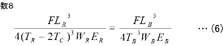
コア基板Bの長さLBと埋設層Rの長さLR、およびコア基板の幅WBと埋設層Rの幅WRとが等しいとして、(6)式をTRについて解くと(7)式となる。

(7)式は、コア基板Bおよび埋設層の第2部分R2のたわみが、同じ大きさで逆方向であるとき、すなわちコア基板Bと埋設層の第2部分R2とが、互いの振動を打ち消し合うように振動する場合を表す。
ただし、実際には、第2部分R2と第1部分R1の上側の層とは、振動する際に、考慮されていない要因により相互に影響を及ぼし合う。同様にコア基板Bと第1部分R1の下側の層とは、振動する際に、考慮されていない要因により相互に影響を及ぼし合う。そのため、第2部分R2とコア基板Bとは、それぞれ単独に振動するものとして扱うことができない。
そのため、上記の相互作用を考慮して、埋設層の厚みTRおよびコア基板の厚みTBが変数であり、コア基板の弾性率EBと埋設層の弾性率ERとの比EB/ERおよび静電容量発現部の中心の高さTCが定数である一次方程式を仮定した。そして、(7)式では1/3となっているコア基板の弾性率EBと埋設層の弾性率ERとの比EB/ERの累乗の指数mをフィッティングパラメータとして、実際の振動状態に基づき、振動条件式を求めた。すなわち、上記の一次方程式は(8)式によって表される。

ここで、電子部品内蔵基板1の振動を示す振動パラメータVPは、(8)式の右辺を埋設層の弾性率ERで除した(9)式によって表される。

振動パラメータVPが1のとき、電子部品内蔵基板1の振動が最も小さくなる。一方、振動パラメータVPが1から離れるほど、電子部品内蔵基板1の振動が大きくなる。
本件発明者は、鋭意研究を重ねた結果、振動パラメータVPを制御することによって、電子部品内蔵基板の振動と、それに基づく可聴音の発生を制御できることを見出し、この発明を為すに至った。その際、電子部品10が埋設層Rに埋設されていない状態の基板の振動に対応する音圧の大きさを基準音圧とし、基準音圧よりも小さくなる範囲に対応する振動パラメータVPの範囲を規定した。音圧とは、可聴域内に発生する振動のうち、最も大きな振幅を音の大きさに変換したものである。
すなわち、本件発明者は、この発明において、上記の技術思想に基づき、基準音圧よりも小さくなる振動パラメータVPの上限値をAおよび下限値をB、ならびに累乗の指数mの値を規定した。
上記の振動パラメータVPの上限値Aおよび下限値B、ならびに累乗の指数mの値の規定の仕方について、以下で具体的に説明する。
電子部品内蔵基板1の一方主面に設けられた埋設層の厚みTRと、振動の大きさに対応する音圧との関係を、種々の埋設層の弾性率ERについて有限要素法に基づくシミュレーションにより求めた。そして、シミュレーション結果と対比することにより、振動パラメータVPの上限値Aおよび下限値B、ならびに累乗の指数mの値を決定した。
図4は、電子部品内蔵基板1の一方主面に設けられた埋設層の厚みTRと、振動の大きさに対応する音圧との関係を、有限要素法に基づくシミュレーションにより求めた結果を示すグラフである。
音圧は、電子部品10のL方向(図2(B)においてコア基板Bと水平な方向)に発生した音(いわゆる「鳴き」)の大きさを表している。シミュレーションにおいて、電子部品10は、内部電極15、16がコア基板Bと平行となるように実装されたものと仮定されている。
また、コア基板の厚みTBは0.8mm、コア基板の弾性率EBは20GPa、静電容量発現部の中心の高さTCは0.315mmとしている。コア基板Bの弾性率EBは、一般的に用いられるガラスエポキシ基板の弾性率(曲げ弾性率)として妥当と思われる値を用いている。電子部品10は、L方向の長さが24mmの埋設層R内に埋設されているとして、埋設層の厚みTRの変化による音圧の変化を計算した。
図4では、埋設層の弾性率ERを15GPa、25GPaおよび35GPaとしたときの3通りのシミュレーション結果が示されている。まず、振動パラメータVPの累乗の指数mの値を決定するために、コア基板Bと埋設層の第2部分R2とが、互いの振動を打ち消し合って音圧の極小となっている埋設層の厚みTRに着目した。埋設層の弾性率ERが上記の各値であるとき、音圧が極小値となる埋設層の厚みTRはそれぞれ約1.6mm、約1.3mmおよび約1.15mmである。
ここで、累乗の指数mを3/4とし、埋設層の弾性率ERを15GPa、25GPaおよび35GPaとして(9)式により埋設層の厚みTRを計算すると、それぞれ1.62mm、1.31mmおよび1.16mmとなり、シミュレーション結果を非常によく再現している。
また、互いの振動を完全に打ち消し合わなくても、電子部品内蔵基板1の振動の大きさ(それに伴う音の大きさ)は、厚みTRの埋設層Rが形成されることにより、埋設層Rがない状態よりも小さくなればよい。
そのような埋設層の厚みTRの範囲を図4に示したシミュレーション結果から求めた。その結果、埋設層の弾性率ERを15GPaとしたとき、TRが1.3~2.1のとき、電子部品内蔵基板1の振動の大きさが、埋設層Rがない状態よりも小さくなることが分かった。同様に、埋設層の弾性率ERを25GPaおよび35GPaとしたとき、それぞれTRが1.1~1.55および1.0~1.3のとき、電子部品内蔵基板1の振動の大きさが、埋設層Rがない状態よりも小さくなることが分かった。
以上のようにして振動パラメータVPを図4のシミュレーション結果に合わせ込むと、累乗の指数mが3/4、振動パラメータVPの上限値Aが1.2、下限値Bが0.8となることが分かった。
これらの値は、簡略化された構造において、コア基板Bと埋設層の第2部分R2とが、前述の埋設層の第1部分R1との相互作用を含め、静電容量発現部CPの中心面から見て、互いの振動を打ち消し合うように振動する条件を表していると考えられる。
すなわち、埋設層の厚みTRと、埋設層の弾性率ERと、コア基板の厚みTBと、コア基板の弾性率EBと、コア基板Bの一方主面を基準面としたときの静電容量発現部の中心の高さTCとの関係が、(1)式を満足するときに、電子部品内蔵基板1の振動が低減され、さらに振動による可聴音の発生が防止または低減される。したがって、電子部品内蔵基板1の振動による可聴音の音圧が、基準音圧よりも小さくなる。

また、上記のTRおよびERの範囲、ならびにTB、TCおよびEBの値から、埋設層の厚みTRと、埋設層の弾性率ERと、コア基板の厚みTBと、コア基板の弾性率EBと、コア基板の一方主面を基準面としたときの静電容量発現部の中心の高さTCとが、上記の(1)式に加えて、(2)式~(4)式をさらに満足するときに、電子部品内蔵基板1の振動は確実に低減され、さらに振動による可聴音の発生が確実に防止または低減される。

<実施形態の変形例>
この発明の実施形態に係る電子部品内蔵基板の変形例1Aについて、図5を用いて説明する。
この発明の実施形態に係る電子部品内蔵基板の変形例1Aについて、図5を用いて説明する。
図5は、この発明の実施形態に係る電子部品内蔵基板の変形例1Aの断面図である。図5(A)は図1のY1-Y1線を含む面の矢視断面図(図2(A))に相当する。図5(B)は図1のX1-X1線を含む面の矢視断面図(図2(B))に相当する。
この発明の実施形態に係る電子部品内蔵基板の変形例1Aは、電子部品10の第1のセラミック保護部P1の厚みが、第2のセラミック保護部P2の厚みより厚くなっている。さらに、電子部品10は、第1のセラミック保護部P1がコア基板Bの一方主面側となるように実装されている。なお、コア基板Bは、前述の実施形態と同様に、簡略化して図示されている。
この発明の実施形態に係る電子部品内蔵基板の変形例1Aでは、電子部品10の静電容量発現部CPの中心が、第1のセラミック保護部P1と第2のセラミック保護部P2とが同じ厚みを有する場合と比べて、コア基板Bの一方主面からより高い位置となっている。
例えば、特開2013-65820号公報には、上記の構造を有する電子部品10をコア基板Bに実装することにより、効果的に電子部品内蔵基板の振動を低減できることが記載されている。
したがって、電子部品内蔵基板1Aにおける各構成要素の寸法が上記の関係を満足することにより、埋設層Rがない場合でも、既にある程度まで低減されている電子部品内蔵基板の振動をさらに低減させ、振動による可聴音の発生をさらに確実に防止または低減することができる。
<電子部品内蔵基板の製造方法>
この発明の実施形態に係る電子部品内蔵基板1の製造方法の一例について、図6および図7を用いて説明する。図6および図7は、電子部品内蔵基板1の製造方法の一例において順次行なわれる実装工程および埋設層形成工程をそれぞれ模式的に示す図である。なお、図6および図7の各図は、図1のY1-Y1線を含む面の矢視断面図(図2(A))に相当する。
この発明の実施形態に係る電子部品内蔵基板1の製造方法の一例について、図6および図7を用いて説明する。図6および図7は、電子部品内蔵基板1の製造方法の一例において順次行なわれる実装工程および埋設層形成工程をそれぞれ模式的に示す図である。なお、図6および図7の各図は、図1のY1-Y1線を含む面の矢視断面図(図2(A))に相当する。
<実装工程>
図6(A)および(B)は、電子部品内蔵基板1の製造方法の実装工程を模式的に示す図である。実装工程により、電子部品10は、コア基板Bの一方主面に実装された状態となる。
図6(A)および(B)は、電子部品内蔵基板1の製造方法の実装工程を模式的に示す図である。実装工程により、電子部品10は、コア基板Bの一方主面に実装された状態となる。
図6(A)は、電子部品10と、電子部品10を実装するコア基板Bとを準備する段階を示す。電子部品10は、前述の構造を有し、電圧印加時に歪みが発生する積層セラミックコンデンサである。コア基板10は、電子部品10を接合するための実装ランドL11およびL12(L12は不図示)を一方主面に備えている。
図6(B)は、電子部品10を、はんだSを用いて実装ランドL11およびL12に接合することにより、コア基板10の一方主面に実装した段階を示す。
このとき、静電容量発現部CPの中心面は、コア基板Bの一方主面を基準面としたとき、高さTCとなっている。
<埋設層形成工程>
図7(A)および(B)は、電子部品内蔵基板1の製造方法の埋設層形成工程を模式的に示す図である。埋設層形成工程により、コア基板Bの一方主面に、電子部品10が埋設されるように埋設層Rが設けられた状態となる。
図7(A)および(B)は、電子部品内蔵基板1の製造方法の埋設層形成工程を模式的に示す図である。埋設層形成工程により、コア基板Bの一方主面に、電子部品10が埋設されるように埋設層Rが設けられた状態となる。
図7(A)は、電子部品10が実装されたコア基板Bの一方主面に、例えばディスペンサDにより、一点鎖線で表される所定の厚みとなるように、液状の樹脂LRを塗布する段階を示す。
塗布に用いる装置は、上記のディスペンサDに限らず、既存の塗布装置を用いることができる。例えば、カーテンコーターやスピンコーターなどの種々のコーターを用いてもよい。
また、液状の樹脂LRは、単一の樹脂材料からなるものに限らず、樹脂材料中にフィラーとしてガラス材料やシリカなどのフィラーを含むものを用いることができる。
さらに、埋設層Rは、図7(A)のような液状の樹脂LRを塗布する方法に限らず、半硬化状態でシート状のプリプレグをコア基板Bの一方主面に載置し、電子部品10が埋設されるように押圧することにより形成してもよい。
図7(B)は、電子部品10が埋設された液状の樹脂LRを加熱し、硬化させることにより、硬化後の埋設層Rとした段階を示す。
このとき、硬化後の埋設層Rは、その厚みTRと、埋設層の弾性率ERと、コア基板の厚みTBと、コア基板の弾性率EBと、静電容量発現部の中心の高さTCとが、(1)式を満足するように形成される。

上記の(1)式で表される関係は、前述のように、コア基板Bと埋設層の第2部分R2とが、埋設層の第1部分R1との相互作用を含め、静電容量発現部CPの中心面から見て、互いの振動を打ち消し合うように振動する条件を表していると考えられる。
すなわち、電子部品内蔵基板1における各構成要素が(1)式で表される関係を満足することにより、電子部品内蔵基板1の振動が低減され、さらに振動による可聴音の発生が防止または低減される。
したがって、埋設層形成工程において、電子部品内蔵基板1における各構成要素が(1)式で表される関係を満足するように埋設層Rを形成することにより、前述の可聴周波数域内での振動がより小さく、可聴音の発生が確実に防止または低減された電子部品内蔵基板を、効率的に製造することができる。
また、埋設層形成工程において、埋設層Rは、電子部品内蔵基板1における各構成要素が、上記の(1)式に加えて、(2)式~(4)式をさらに満足するように設けられることが好ましい。
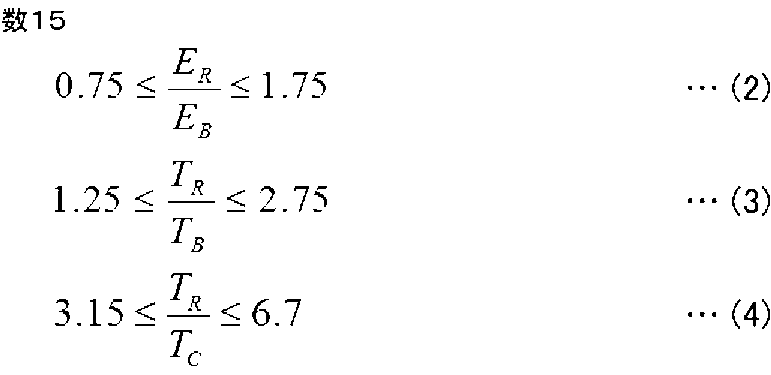
埋設層形成工程において、電子部品内蔵基板1における各構成要素が(1)式~(4)式で表される関係を満足するように埋設層Rを形成することにより、前述の可聴周波数域内での振動がより小さく、可聴音の発生が確実に防止または低減された電子部品内蔵基板を、効率的に製造することができる。
埋設層の厚みTRの調整は、液状の樹脂LRの硬化時の体積変化を見込んで、液状の樹脂LRを硬化後に厚みTRとなるように塗布してもよい。また、予め多めに液状の樹脂LRを塗布し、硬化後に余分な樹脂を除去することにより、埋設層の厚みTRを所望の値としてもよい。
なお、この発明は上記の実施形態に限定されるものではなく、この発明の範囲内において、種々の応用、変形を加えることが可能である。
1 電子部品内蔵基板、10 電子部品(積層セラミックコンデンサ)、11 セラミック積層体、12 第1の外部電極、13 第2の外部電極、14 セラミック誘電体層、15 第1の内部電極、16 第2の内部電極、B コア基板、CP 静電容量発現部、P1 第1のセラミック保護部、P2 第2のセラミック保護部、R 埋設層、TC 静電容量発現部の中心の高さ、TB コア基板の厚み、EB コア基板の弾性率、TR 埋設層の厚み、ER 埋設層の弾性率。
Claims (5)
- 平行な一方主面と他方主面とを有するコア基板と、
前記コア基板の一方主面に実装された、少なくとも1つの電子部品と、
前記コア基板の一方主面に、前記電子部品を埋設し、かつ外表面が前記コア基板の一方主面と平行となるように設けられた埋設層と、を備える電子部品内蔵基板であって、
前記電子部品は、誘電体層が第1の内部電極と第2の内部電極との間に挿入されてなるコンデンサ素子が積層された静電容量発現部と、前記静電容量発現部を挟む第1の保護部および第2の保護部とを含む積層体と、前記積層体の表面に設けられ、前記第1の内部電極と接続される第1の外部電極および前記第2の内部電極と接続される第2の外部電極と、を備える積層コンデンサであり、
埋設層の厚みTRと、埋設層の弾性率ERと、コア基板の厚みTBと、コア基板の弾性率EBと、前記コア基板の一方主面を基準面としたときの静電容量発現部の中心の高さTCとが、

- 前記埋設層の厚みTRと、前記埋設層の弾性率ERと、前記コア基板の厚みTBと、前記コア基板の弾性率EBと、前記コア基板の一方主面を基準面としたときの静電容量発現部の中心の高さTCとが、
- 前記電子部品の前記第1の保護部の厚みは、前記第2の保護部の厚みより厚く、
前記電子部品は、前記第1の保護部が前記コア基板の一方主面側となるように実装されていることを特徴とする、請求項1または2に記載の電子部品内蔵基板。 - 平行な一方主面と他方主面とを有するコア基板と、前記コア基板の一方主面に実装された、少なくとも1つの電子部品と、前記コア基板の一方主面に、前記電子部品を埋設し、かつ外表面が前記コア基板の一方主面と平行となるように設けられた埋設層と、を備える電子部品内蔵基板の製造方法であって、
前記電子部品は、誘電体層が第1の内部電極と第2の内部電極との間に挿入されてなるコンデンサ素子が積層された静電容量発現部と、前記静電容量発現部を挟む第1の保護部および第2の保護部とを含む積層体と、前記積層体の表面に設けられ、前記第1の内部電極と接続される第1の外部電極および前記第2の内部電極と接続される第2の外部電極と、を備える積層コンデンサであり、
前記コア基板の一方主面に、前記電子部品を実装する実装工程と、
埋設層の厚みTRと、埋設層の弾性率ERと、コア基板の厚みTBと、コア基板の弾性率EBと、前記コア基板の一方主面を基準面としたときの静電容量発現部の中心の高さTCとが、

を備えることを特徴とする、電子部品内蔵基板の製造方法。 - 前記埋設層形成工程において、前記埋設層は、前記埋設層の厚みTRと、前記埋設層の弾性率ERと、前記コア基板の厚みTBと、前記コア基板の弾性率EBと、前記コア基板の一方主面を基準面としたときの静電容量発現部の中心の高さTCとが、

Priority Applications (1)
| Application Number | Priority Date | Filing Date | Title |
|---|---|---|---|
| PCT/JP2016/065049 WO2017199436A1 (ja) | 2016-05-20 | 2016-05-20 | 電子部品内蔵基板およびその製造方法 |
Applications Claiming Priority (1)
| Application Number | Priority Date | Filing Date | Title |
|---|---|---|---|
| PCT/JP2016/065049 WO2017199436A1 (ja) | 2016-05-20 | 2016-05-20 | 電子部品内蔵基板およびその製造方法 |
Publications (1)
| Publication Number | Publication Date |
|---|---|
| WO2017199436A1 true WO2017199436A1 (ja) | 2017-11-23 |
Family
ID=60325817
Family Applications (1)
| Application Number | Title | Priority Date | Filing Date |
|---|---|---|---|
| PCT/JP2016/065049 Ceased WO2017199436A1 (ja) | 2016-05-20 | 2016-05-20 | 電子部品内蔵基板およびその製造方法 |
Country Status (1)
| Country | Link |
|---|---|
| WO (1) | WO2017199436A1 (ja) |
Citations (4)
| Publication number | Priority date | Publication date | Assignee | Title |
|---|---|---|---|---|
| JP2007142355A (ja) * | 2005-10-18 | 2007-06-07 | Matsushita Electric Ind Co Ltd | 電子部品内蔵モジュール |
| JP2012248581A (ja) * | 2011-05-25 | 2012-12-13 | Tdk Corp | 積層コンデンサ及び積層コンデンサの製造方法 |
| WO2016035590A1 (ja) * | 2014-09-01 | 2016-03-10 | 株式会社 村田製作所 | 電子部品内蔵基板 |
| JP2016092176A (ja) * | 2014-11-04 | 2016-05-23 | 株式会社村田製作所 | 電子部品内蔵基板およびその製造方法 |
-
2016
- 2016-05-20 WO PCT/JP2016/065049 patent/WO2017199436A1/ja not_active Ceased
Patent Citations (4)
| Publication number | Priority date | Publication date | Assignee | Title |
|---|---|---|---|---|
| JP2007142355A (ja) * | 2005-10-18 | 2007-06-07 | Matsushita Electric Ind Co Ltd | 電子部品内蔵モジュール |
| JP2012248581A (ja) * | 2011-05-25 | 2012-12-13 | Tdk Corp | 積層コンデンサ及び積層コンデンサの製造方法 |
| WO2016035590A1 (ja) * | 2014-09-01 | 2016-03-10 | 株式会社 村田製作所 | 電子部品内蔵基板 |
| JP2016092176A (ja) * | 2014-11-04 | 2016-05-23 | 株式会社村田製作所 | 電子部品内蔵基板およびその製造方法 |
Similar Documents
| Publication | Publication Date | Title |
|---|---|---|
| CN106688315B (zh) | 电子部件内置基板 | |
| KR20130008086A (ko) | 음향 발생기 | |
| TW201127085A (en) | Microphone unit | |
| CN103444205A (zh) | 声发生器及使用了该声发生器的声发生装置 | |
| JP5934303B2 (ja) | 音響発生器、音響発生装置及び電子機器 | |
| CN103765922A (zh) | 声发生器、声发生装置以及电子设备 | |
| WO2017159377A1 (ja) | 積層コンデンサ内蔵基板 | |
| US20150136464A1 (en) | Electronic Device | |
| JP6424570B2 (ja) | 電子部品内蔵基板およびその製造方法 | |
| JP6256306B2 (ja) | 電子部品内蔵基板およびその製造方法 | |
| WO2016035590A1 (ja) | 電子部品内蔵基板 | |
| WO2014045719A1 (ja) | 音響発生器、音響発生装置及び電子機器 | |
| JP5878980B2 (ja) | 音響発生器、音響発生装置および電子機器 | |
| WO2017199436A1 (ja) | 電子部品内蔵基板およびその製造方法 | |
| JP5726375B2 (ja) | 音響発生器、音響発生装置および電子機器 | |
| JP5534938B2 (ja) | 圧電スピーカ | |
| JP6375889B2 (ja) | 電子部品内蔵基板およびその製造方法 | |
| US20190035557A1 (en) | Mounting structure and multilayer capacitor built-in substrate | |
| JP5890209B2 (ja) | 音響発生装置 | |
| JP5933392B2 (ja) | 音響発生器、音響発生装置及び電子機器 | |
| JP2014049907A (ja) | 圧電素子製造方法、内部電極、圧電素子及び圧電素子製造装置 | |
| JP2014039094A (ja) | 音響発生器、音響発生装置及び電子機器 | |
| JP2018148167A (ja) | 回路基板、回路基板の製造方法及び電子装置 |
Legal Events
| Date | Code | Title | Description |
|---|---|---|---|
| NENP | Non-entry into the national phase |
Ref country code: DE |
|
| 121 | Ep: the epo has been informed by wipo that ep was designated in this application |
Ref document number: 16902455 Country of ref document: EP Kind code of ref document: A1 |
|
| 122 | Ep: pct application non-entry in european phase |
Ref document number: 16902455 Country of ref document: EP Kind code of ref document: A1 |
|
| NENP | Non-entry into the national phase |
Ref country code: JP |