WO2017191721A1 - 弾性波装置、デュプレクサ及びマルチプレクサ - Google Patents
弾性波装置、デュプレクサ及びマルチプレクサ Download PDFInfo
- Publication number
- WO2017191721A1 WO2017191721A1 PCT/JP2017/014003 JP2017014003W WO2017191721A1 WO 2017191721 A1 WO2017191721 A1 WO 2017191721A1 JP 2017014003 W JP2017014003 W JP 2017014003W WO 2017191721 A1 WO2017191721 A1 WO 2017191721A1
- Authority
- WO
- WIPO (PCT)
- Prior art keywords
- acoustic wave
- wave element
- elastic wave
- elastic
- acoustic
- Prior art date
- Legal status (The legal status is an assumption and is not a legal conclusion. Google has not performed a legal analysis and makes no representation as to the accuracy of the status listed.)
- Ceased
Links
Images





Classifications
-
- H—ELECTRICITY
- H03—ELECTRONIC CIRCUITRY
- H03H—IMPEDANCE NETWORKS, e.g. RESONANT CIRCUITS; RESONATORS
- H03H9/00—Networks comprising electromechanical or electro-acoustic elements; Electromechanical resonators
- H03H9/25—Constructional features of resonators using surface acoustic waves
-
- H—ELECTRICITY
- H03—ELECTRONIC CIRCUITRY
- H03H—IMPEDANCE NETWORKS, e.g. RESONANT CIRCUITS; RESONATORS
- H03H9/00—Networks comprising electromechanical or electro-acoustic elements; Electromechanical resonators
- H03H9/46—Filters
- H03H9/64—Filters using surface acoustic waves
-
- H—ELECTRICITY
- H03—ELECTRONIC CIRCUITRY
- H03H—IMPEDANCE NETWORKS, e.g. RESONANT CIRCUITS; RESONATORS
- H03H9/00—Networks comprising electromechanical or electro-acoustic elements; Electromechanical resonators
- H03H9/70—Multiple-port networks for connecting several sources or loads, working on different frequencies or frequency bands, to a common load or source
- H03H9/72—Networks using surface acoustic waves
-
- H—ELECTRICITY
- H10—SEMICONDUCTOR DEVICES; ELECTRIC SOLID-STATE DEVICES NOT OTHERWISE PROVIDED FOR
- H10W—GENERIC PACKAGES, INTERCONNECTIONS, CONNECTORS OR OTHER CONSTRUCTIONAL DETAILS OF DEVICES COVERED BY CLASS H10
- H10W74/00—Encapsulations, e.g. protective coatings
- H10W74/40—Encapsulations, e.g. protective coatings characterised by their materials
-
- H—ELECTRICITY
- H10—SEMICONDUCTOR DEVICES; ELECTRIC SOLID-STATE DEVICES NOT OTHERWISE PROVIDED FOR
- H10W—GENERIC PACKAGES, INTERCONNECTIONS, CONNECTORS OR OTHER CONSTRUCTIONAL DETAILS OF DEVICES COVERED BY CLASS H10
- H10W90/00—Package configurations
- H10W90/701—Package configurations characterised by the relative positions of pads or connectors relative to package parts
- H10W90/721—Package configurations characterised by the relative positions of pads or connectors relative to package parts of bump connectors
- H10W90/724—Package configurations characterised by the relative positions of pads or connectors relative to package parts of bump connectors between a chip and a stacked insulating package substrate, interposer or RDL
Definitions
- the present invention relates to an acoustic wave device, a duplexer, and a multiplexer including a plurality of acoustic wave elements.
- An elastic wave device including an elastic wave element is used, for example, in a duplexer or a multiplexer constituting a communication module of a mobile communication terminal.
- Patent Document 1 discloses an acoustic wave device (demultiplexer) in which a transmission acoustic wave element and a reception acoustic wave element are mounted on a mounting substrate.
- the present invention has been made in view of such problems, and an object thereof is to provide an elastic wave device and the like that can suppress a temperature rise and improve power durability.
- an acoustic wave device includes a plurality of acoustic wave elements and a mounting substrate on which the plurality of acoustic wave elements are mounted.
- a first acoustic wave element and a second acoustic wave element positioned adjacent to the first acoustic wave element on the mounting substrate, wherein the first acoustic wave element is larger than the second acoustic wave element. It is an element to which electric power is applied, and at least a part of the outer surface of the first acoustic wave element has a larger surface roughness than the outer surface of the second acoustic wave element.
- the surface area of the outer surface of the first acoustic wave element is large, and the first acoustic wave element
- the structure is easy to dissipate heat. Thereby, the temperature rise of the 1st elastic wave element with large received electric power can be suppressed, and the electric power durability of an elastic wave apparatus can be improved.
- the surface roughness of the outer surface of the second acoustic wave element is smaller than the surface roughness of the outer surface of the first acoustic wave element, that is, the surface area of the outer surface of the second acoustic wave element is small and heat absorption is difficult. .
- the heat generated in the first acoustic wave element is hardly absorbed by the second acoustic wave element, the temperature rise of the second acoustic wave element is suppressed, and the power durability of the acoustic wave device can be improved.
- Each of the first acoustic wave element and the second acoustic wave element includes a side surface continuous with each side of one main surface facing the mounting surface of the mounting substrate, and at least one of the first acoustic wave element The side surface may have a larger surface roughness than the side surface of the second acoustic wave element.
- the first elastic wave element has a larger surface area than the second elastic wave element, and has a structure that easily dissipates heat. Thereby, the temperature rise of a 1st elastic wave element can be suppressed and the electric power durability of an elastic wave apparatus can be improved.
- each of the first acoustic wave element and the second acoustic wave element may include a piezoelectric substrate and an IDT electrode provided on the piezoelectric substrate, and the side surface may be a side surface of the piezoelectric substrate.
- the surface roughness of the side surface of the piezoelectric substrate By increasing the surface roughness of the side surface of the piezoelectric substrate, the temperature rise of the first acoustic wave element can be suppressed and the power durability of the acoustic wave device can be improved.
- a sealing portion provided on the mounting substrate may be provided so as to fill a space between the first acoustic wave element and the second acoustic wave element.
- the second acoustic wave element Since the outer surface of the second acoustic wave element has a smaller surface roughness than the outer surface of the first acoustic wave element and is difficult to absorb heat, the second acoustic wave element is sealed between the first acoustic wave element and the second acoustic wave element. Even if there is a stop, heat generated in the first acoustic wave element is not easily absorbed by the second acoustic wave element. Thereby, the temperature rise of a 2nd acoustic wave element can be suppressed and the power durability of an acoustic wave apparatus can be improved.
- first elastic wave element and the second elastic wave element are viewed in plan, the first elastic wave element and the second elastic wave element are rectangular, and the second elastic wave element is the second elastic wave element.
- the shortest side of the wave element may be arranged to face the first acoustic wave element.
- the area of the second acoustic wave element that absorbs heat generated by the first acoustic wave element is reduced, and the amount of heat absorbed by the second acoustic wave element can be reduced.
- the temperature rise of a 2nd acoustic wave element can be suppressed and the power durability of an acoustic wave apparatus can be improved.
- the first acoustic wave element and the second acoustic wave element are viewed in plan, the first acoustic wave element and the second acoustic wave element are rectangular, and the first acoustic wave element is the first elastic wave element.
- the shortest side of the wave element may be arranged to face the second acoustic wave element.
- the area of the first acoustic wave element facing the second acoustic wave element is reduced, and the amount of heat transfer from the first acoustic wave element to the second acoustic wave element can be reduced.
- the temperature rise of a 2nd acoustic wave element can be suppressed and the power durability of an acoustic wave apparatus can be improved.
- the first acoustic wave element may include a transmitting element, and the second acoustic wave element may be a receiving element.
- the first acoustic wave element including the transmitting element that requires a large amount of power is easily radiated, the temperature rise of the first acoustic wave element is suppressed and the power durability of the acoustic wave device is improved. be able to.
- the second acoustic wave element which is a receiving element to which small electric power is applied, has a structure that hardly absorbs heat, the temperature rise of the second acoustic wave element can be suppressed, and the power durability of the acoustic wave device can be improved.
- each of the plurality of acoustic wave elements may be a surface acoustic wave element or a boundary acoustic wave element.
- the temperature rise of the elastic wave device including the surface acoustic wave element or the boundary acoustic wave element can be suppressed, and the power durability can be improved.
- duplexer according to one aspect of the present invention is configured by the elastic wave device.
- the temperature rise of the duplexer constituted by the elastic wave device can be suppressed, and the power durability can be improved.
- the multiplexer according to one aspect of the present invention is configured by the elastic wave device.
- the elastic wave device of the present invention can suppress temperature rise and improve power durability.
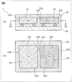
- FIG. 1 is an external view of an acoustic wave device according to an embodiment.
- FIG. 2 is a cross-sectional view of the acoustic wave device according to the embodiment, (a) is a cross-sectional view obtained by cutting along a plane including a line IIa-IIa in FIG. 1, and (b) is a cross-sectional view in (a).
- FIG. 2 is a cross-sectional view (a cross-sectional view when the elastic wave device is viewed in plan) obtained by cutting along a plane including a line IIb-IIb.
- FIG. 3 is a cross-sectional view of an acoustic wave element included in the acoustic wave device shown in FIG. FIG.
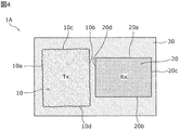
- FIG. 4 is a cross-sectional view of the elastic wave device according to the first modification of the embodiment when viewed in plan.
- FIG. 5 is a cross-sectional view of the elastic wave device according to the second modification of the embodiment when viewed in plan.
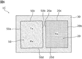
- FIG. 6 is a cross-sectional view of the elastic wave device according to the third modification of the embodiment when viewed in plan.
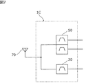
- FIG. 7 is a diagram illustrating a multiplexer configured by the acoustic wave device according to the third modification of the embodiment.
- FIG. 8 is a cross-sectional view of the elastic wave device according to Modification 4 of the embodiment when viewed in plan.
- FIG. 9 is a cross-sectional view of the acoustic wave device according to the fifth modification of the embodiment when viewed in plan.
- the elastic wave device includes a plurality of elastic wave elements (surface acoustic wave elements or boundary acoustic wave elements), and is used, for example, in a duplexer, a multiplexer, or a communication module built in a mobile communication terminal or the like.
- an elastic wave device constituting a duplexer will be described as an example.
- FIG. 1 is an external view of an acoustic wave device 1 according to the present embodiment.
- 2 is a cross-sectional view of the acoustic wave device shown in FIG. 1, wherein (a) is a cross-sectional view obtained by cutting along the plane including the IIa-IIa line in FIG. 1, and (b) is IIb in (a).
- FIG. 6 is a cross-sectional view obtained by cutting along a plane including a line -IIb.
- the acoustic wave device 1 includes a first acoustic wave element 10 (hereinafter referred to as an acoustic wave element 10), a second acoustic wave element 20 (hereinafter referred to as an acoustic wave element 20), and acoustic wave elements 10 and 20.
- Mounting board 40 The acoustic wave element 10 is a transmission filter, and the acoustic wave element 20 is a reception filter.
- the acoustic wave elements 10 and 20 are adjacent to each other on the mounting substrate 40.
- As the mounting substrate 40 a ceramic substrate or a glass epoxy substrate is used.
- the elastic wave device 1 has a sealing portion 30.
- the sealing portion 30 is provided on the mounting substrate 40 so as to fill the space between the acoustic wave element 10 and the acoustic wave element 20 and to cover the acoustic wave elements 10 and 20.
- the sealing part 30 is comprised by resin materials, such as an epoxy, for example.
- the basic structure of the acoustic wave elements 10 and 20 will be described using the acoustic wave element 10 as an example.
- FIG. 3 is a cross-sectional view of the acoustic wave element 10 included in the acoustic wave device 1.
- the acoustic wave element 10 is a WLP (Wafer Level Package) type surface acoustic wave device, and includes a piezoelectric substrate 11, an IDT (Inter Digital Transducer) electrode 12, a wiring electrode 13, a cover layer 15, a columnar electrode 14, a solder bump 16, And a support layer 17.
- the acoustic wave element 10 has a hollow space 19 surrounded by a piezoelectric substrate 11, a support layer 17 erected around the piezoelectric substrate 11, and a cover layer 15 disposed on the support layer 17. have.
- the piezoelectric substrate 11 is a piezoelectric body that constitutes the substrate of the acoustic wave element 10, and is made of, for example, a piezoelectric single crystal such as lithium tantalate (LiTaO 3 ), lithium niobate (LiNbO 3 ), or quartz, or piezoelectric ceramics. .
- a piezoelectric single crystal such as lithium tantalate (LiTaO 3 ), lithium niobate (LiNbO 3 ), or quartz, or piezoelectric ceramics.
- the IDT electrode 12 is a comb-shaped electrode that is provided on the main surface of the piezoelectric substrate 11 and excites surface acoustic waves.
- a metal or alloy such as Ti, Al, Cu, Au, Pt, Ag, Pd, or Ni, or And a laminate of these metals or alloys.
- the wiring electrode 13 is an electrode that constitutes a part of a wiring path that connects the IDT electrode 12 and the outside of the acoustic wave element 10, and is made of, for example, the same material as the IDT electrode 12.
- the support layer 17 is a layer that is erected around the region where the IDT electrode 12 is provided on the main surface of the piezoelectric substrate 11 and is higher than the height of the IDT electrode 12.
- the support layer 17 is made of, for example, a material containing at least one of polyimide, epoxy, benzocyclobutene (BCB), polybenzoxazole (PBO), metal, and silicon oxide.
- the cover layer 15 is a layer that is disposed on the support layer 17 and covers the IDT electrode 12 through the hollow space 19 and is made of a material containing at least one of polyimide, epoxy, BCB, PBO, metal, and silicon oxide. Is done.
- the columnar electrode 14 is an electrode that forms part of a wiring path that connects the wiring electrode 13 and the outside and is formed so as to penetrate the support layer 17 and the cover layer 15.
- the columnar electrode 14 is the same as the IDT electrode 12. Composed of materials.
- the acoustic wave element 10 is provided with solder bumps 16 so as to be exposed downward from the cover layer 15.
- the acoustic wave element 10 is soldered to the mounting substrate 40 via the solder bumps 16.
- the acoustic wave elements 10 and 20 are adjacent to each other via the sealing portion 30.
- the acoustic wave elements 10 and 20 include four side surfaces that are continuous with each side of the one main surface that faces the mounting surface of the mounting substrate 40.
- the acoustic wave element 10 has a rectangular shape in plan view, the side surfaces 10a and 10b are long sides, and the side surfaces 10c and 10d are short sides.
- the acoustic wave element 20 has a rectangular shape in plan view, the side surfaces 20a and 20b are long sides, and the side surfaces 20c and 20d are short sides.
- the side surface 10 b corresponding to the long side of the acoustic wave element 10 and the side surface 20 a corresponding to the long side of the acoustic wave element 20 face each other.
- the acoustic wave element 10 is an element that requires larger power than the acoustic wave element 20. That is, the elastic wave element 10 has a higher rated power than the elastic wave element 20. Specifically, the acoustic wave element 10 is a transmission element such as a transmission filter, and the acoustic wave element 20 is a reception element such as a reception filter. When the duplexer configured by the elastic wave device 1 is used, the elastic wave element 10 that is a transmitting element is supplied with larger power than the elastic wave element 20 that is a receiving element. Therefore, the acoustic wave element 10 generates heat more easily than the acoustic wave element 20 and is likely to increase in temperature.
- the outer surface of the acoustic wave element 10 has a larger surface roughness than the outer surface of the acoustic wave element 20.
- the side surfaces 10 a to 10 d which are part of the outer surface of the acoustic wave element 10 have a larger surface roughness than the side surfaces 20 a to 20 d of the acoustic wave element 20. Therefore, the side surfaces 10a to 10d of the acoustic wave device 10 have a larger surface area than the side surfaces 20a to 20d of the acoustic wave device 20, and have a structure that facilitates heat dissipation.
- the side surfaces 20a to 20d of the acoustic wave element 20 have a smaller surface area than the side surfaces 10a to 10d of the acoustic wave element 10, and are less likely to absorb heat (receive heat).
- the surface roughness in the above is arithmetic average roughness Ra based on JIS B0601.
- the acoustic wave device 1 As described above, in the acoustic wave device 1, at least a part of the outer surface of the acoustic wave element 10 has a larger surface roughness than the outer surface of the acoustic wave element 20 and has a structure that easily radiates heat. The temperature rise can be suppressed, and the power durability can be improved.
- the outer surface of the acoustic wave element 20 has a surface roughness smaller than that of the outer surface of the acoustic wave element 10 and is less likely to absorb heat. The power durability of the acoustic wave device 1 can be improved.
- the side surfaces 10a to 10d are side surfaces of the piezoelectric substrate 11 of the acoustic wave element 10
- the side surfaces 20a to 20d are side surfaces of the piezoelectric substrate 11 of the acoustic wave element 20.
- the surface roughness of the side surfaces of the piezoelectric substrate 11 is changed by changing the dicing conditions, that is, the side surfaces 10a to 10d and the side surfaces 20a to 20d. It is possible to adjust the surface roughness.
- FIG. 4 is a cross-sectional view of the elastic wave device 1A according to Modification 1 of the embodiment when viewed in plan.
- the elastic wave element 20 is disposed such that the shortest side of the elastic wave element 20 faces the elastic wave element 10. Specifically, the side surface 20 d corresponding to the short side of the acoustic wave element 20 faces the side surface 10 b corresponding to the long side of the acoustic wave element 10.
- the shortest side of the elastic wave element 20 is disposed to face the elastic wave element 10. Therefore, even when large electric power is applied to the acoustic wave element 10 to generate heat, the area of the acoustic wave element 20 that absorbs heat is reduced, and the amount of heat absorption can be reduced. Thereby, the temperature rise of the acoustic wave element 20 can be suppressed, and the power durability of the acoustic wave device 1A can be improved.
- FIG. 5 is a cross-sectional view of the acoustic wave device 1B according to Modification 2 of the embodiment when viewed in plan.
- the elastic wave element 10 is arranged such that the shortest side of the elastic wave element 10 faces the elastic wave element 20. Specifically, the side surface 10 c corresponding to the short side of the acoustic wave element 10 faces the side surface 20 d corresponding to the short side of the acoustic wave element 20.
- the shortest side of the elastic wave element 10 is arranged to face the elastic wave element 20. Therefore, even when large electric power is applied to the acoustic wave element 10 to generate heat, the area for transferring heat to the acoustic wave element 20 is reduced, and the amount of heat absorbed by the acoustic wave element 20 can be reduced. Thereby, the temperature rise of the acoustic wave device 20 can be suppressed, and the power durability of the acoustic wave device 1B can be improved.
- FIG. 6 is a cross-sectional view of the elastic wave device 1C according to Modification 3 of the embodiment when viewed in plan.
- FIG. 7 is a diagram illustrating a multiplexer configured by the elastic wave device 1C.
- the elastic wave device (multiplexer) 1C includes an elastic wave element (duplexer) 50 including a transmitting element and a receiving element, and an elastic wave element 20 including a receiving element.
- the acoustic wave element 50 corresponds to the first acoustic wave element in the present embodiment.
- the acoustic wave element 50 has a rectangular shape in plan view, and has side surfaces 50a, 50b, 50c and 50d.
- An antenna 70 is connected to the elastic wave device 1C.
- the elastic wave element 50 is arranged such that the long side of the elastic wave element 50 faces the long side of the elastic wave element 20. Specifically, the side surface 50 b corresponding to the long side of the acoustic wave element 50 faces the side surface 20 a corresponding to the long side of the acoustic wave element 20.
- the elastic wave element 50 since the elastic wave element 50 includes a transmitting element, the elastic wave element 50 requires a larger electric power than the elastic wave element 20. Therefore, in the elastic wave device 1 ⁇ / b> C, at least a part of the outer surface of the elastic wave element 50 has a surface roughness larger than that of the outer surface of the elastic wave element 20, and has a structure that facilitates heat dissipation. Thereby, the temperature rise of the acoustic wave element 50 can be suppressed, and the power durability of the acoustic wave device 1C can be improved.
- FIG. 8 is a cross-sectional view of the acoustic wave device 1D according to the fourth modification of the embodiment when viewed in plan.
- the elastic wave device 1D includes an elastic wave element (duplexer) 50 including a transmitting element and a receiving element, an elastic wave element 20 including a receiving element, and an elastic wave element 10 including a transmitting element.
- an elastic wave element (duplexer) 50 including a transmitting element and a receiving element an elastic wave element 20 including a receiving element
- an elastic wave element 10 including a transmitting element.
- the elastic wave element 50 is arranged such that the long side of the elastic wave element 50 faces the short side of the elastic wave element 20 and the short side of the elastic wave element 10.
- the side surface 50 b corresponding to the long side of the acoustic wave element 50 faces the side surface 20 d corresponding to the short side of the acoustic wave element 20 and the side surface 10 d corresponding to the short side of the acoustic wave element 10. Yes.
- the elastic wave elements 50 and 10 each include a transmitting element, and the elastic wave elements 50 and 10 are applied with a larger electric power than the elastic wave element 20. Therefore, in the acoustic wave device 1 ⁇ / b> D, at least a part of the outer surfaces of the acoustic wave elements 50 and 10 has a larger surface roughness than the outer surface of the acoustic wave element 20, and has a structure that easily radiates heat. Thereby, the temperature rise of the acoustic wave elements 50 and 10 can be suppressed, and the power durability of the acoustic wave device 1D can be improved.
- FIG. 9 is a cross-sectional view of the acoustic wave device 1E according to Modification 5 of the embodiment when viewed in plan.
- the surface acoustic wave device 1E includes a surface acoustic wave element 10 that is a transmission filter, a boundary acoustic wave element 60 that is a transmission filter, one surface acoustic wave element 20 that is a reception filter, and the other surface acoustic wave that is a reception filter. It is comprised with the element 20.
- the boundary acoustic wave element 60 corresponds to the first acoustic wave element in the present embodiment.
- the boundary acoustic wave element 60 has a rectangular shape in plan view, and has side surfaces 60a, 60b, 60c, and 60d.
- the side surface 10c corresponding to the short side of the surface acoustic wave element 10 and the side surface 20d corresponding to the short side of one surface acoustic wave element 20 face each other.
- the side surface 20 c corresponding to the short side of the other surface acoustic wave element 20 and the side surface 60 d corresponding to the short side of the boundary acoustic wave element 60 face each other.
- the side surface 10 b corresponding to the long side of the surface acoustic wave element 10 and the side surface 20 a corresponding to the long side of the other surface acoustic wave element 20 face each other.
- the side surface 20 b corresponding to the long side of one surface acoustic wave element 20 and the side surface 60 a corresponding to the long side of the boundary acoustic wave element 60 face each other.
- Each of the surface acoustic wave element 10 and the boundary acoustic wave element 60 includes a transmitting element, and the surface acoustic wave element 10 and the boundary acoustic wave element 60 are applied with larger electric power than the surface acoustic wave element 20. Therefore, in the acoustic wave device 1E, at least a part of the outer surfaces of the surface acoustic wave element 10 and the boundary acoustic wave element 60 has a surface roughness larger than that of the outer surface of the surface acoustic wave element 20 and is easily radiated. . Thereby, the temperature rise of the surface acoustic wave element 10 and the boundary acoustic wave element 60 can be suppressed, and the power durability of the acoustic wave device 1E can be improved.
- the outer surfaces of the acoustic wave elements 10 and 20 are not limited to the side surfaces 10 a to 10 d and the side surfaces 20 a to 20 d of the piezoelectric substrate 11, but a surface 11 e (surface acoustic wave) opposite to the main surface of the piezoelectric substrate 11. It may be a surface opposite to the propagation surface).
- a surface 11 e surface acoustic wave opposite to the main surface of the piezoelectric substrate 11. It may be a surface opposite to the propagation surface).
- the surface 11e of the piezoelectric substrate 11 is formed by lapping, the surface roughness of the surface 11e of the piezoelectric substrate 11 can be adjusted by changing lapping conditions.
- the present invention can be used, for example, as an elastic wave device constituting a communication module of a mobile communication terminal.
Landscapes
- Physics & Mathematics (AREA)
- Acoustics & Sound (AREA)
- Surface Acoustic Wave Elements And Circuit Networks Thereof (AREA)
Abstract
弾性波装置(1)は、複数の弾性波素子と、複数の弾性波素子が実装される実装基板(40)とを備え、複数の弾性波素子は、第1弾性波素子(10)と、実装基板(40)上で第1弾性波素子(10)の隣に位置する第2弾性波素子(20)とを含み、第1弾性波素子(10)は、第2弾性波素子(20)よりも大きな電力がかかる素子であり、第1弾性波素子(10)の外面の少なくとも一部は、第2弾性波素子(20)の外面よりも表面粗さが大きい。
Description
本発明は、複数の弾性波素子を備える弾性波装置、デュプレクサ及びマルチプレクサに関する。
弾性波素子を備える弾性波装置は、例えば、移動体通信端末の通信モジュールを構成するデュプレクサまたはマルチプレクサに用いられる。
この種の弾性波装置の一例として、特許文献1には、送信用弾性波素子及び受信用弾性波素子を実装基板に実装した弾性波装置(分波器)が開示されている。
しかしながら、特許文献1に記載された弾性波装置では、移動体通信端末を使用して弾性波装置を作動させた場合に、弾性波素子の発熱により温度が上昇し、弾性波素子の特性が変化するという問題がある。
そこで、本発明は、このような問題点に鑑みてなされたものであり、温度上昇を抑制し、耐電力性を向上させることができる弾性波装置等を提供することを目的とする。
上記目的を達成するために、本発明の一形態に係る弾性波装置は、複数の弾性波素子と、前記複数の弾性波素子が実装される実装基板とを備え、前記複数の弾性波素子は、第1弾性波素子と、前記実装基板上で前記第1弾性波素子の隣に位置する第2弾性波素子とを含み、前記第1弾性波素子は、前記第2弾性波素子よりも大きな電力がかかる素子であり、前記第1弾性波素子の外面の少なくとも一部は、前記第2弾性波素子の外面よりも表面粗さが大きい。
このように、第1弾性波素子の外面の少なくとも一部が、第2弾性波素子の外面よりも表面粗さが大きいので、第1弾性波素子の外面の表面積が大きく、第1弾性波素子が放熱しやすい構造となっている。これにより、受給電力が大きい第1弾性波素子の温度上昇を抑制し、弾性波装置の耐電力性を向上させることができる。また、第2弾性波素子の外面の表面粗さが第1弾性波素子の外面の表面粗さよりも小さく、すなわち、第2弾性波素子の外面の表面積が小さく、吸熱しにくい構造となっている。これにより、第1弾性波素子で発生した熱が第2弾性波素子に吸収されにくくなり、第2弾性波素子の温度上昇を抑制し、弾性波装置の耐電力性を向上させることができる。
また、前記第1弾性波素子および前記第2弾性波素子のそれぞれは、前記実装基板の実装面と対向する一方主面の各辺に連なる側面を備え、前記第1弾性波素子の少なくとも1つの側面は、前記第2弾性波素子の側面よりも表面粗さが大きくてもよい。
これによれば、第1弾性波素子は、第2弾性波素子よりも側面の表面積が大きく、放熱しやすい構造となっている。これにより、第1弾性波素子の温度上昇を抑制し、弾性波装置の耐電力性を向上させることができる。
また、前記第1弾性波素子及び前記第2弾性波素子のそれぞれは、圧電基板と前記圧電基板に設けられたIDT電極とを含み、前記側面は、前記圧電基板の側面であってもよい。
これによれば、圧電基板の側面の表面粗さを容易に大きくすることが可能となる。圧電基板の側面の表面粗さを大きくすることで、第1弾性波素子の温度上昇を抑制し、弾性波装置の耐電力性を向上させることができる。
また、さらに、前記第1弾性波素子と前記第2弾性波素子との間を埋めるように、前記実装基板上に設けられる封止部を備えていてもよい。
第2弾性波素子の外面が、第1弾性波素子の外面よりも表面粗さが小さく、吸熱しにくい構造となっているので、第1弾性波素子と第2弾性波素子との間に封止部が存在する場合であっても、第1弾性波素子で発生した熱が、第2弾性波素子に吸収されにくい。これにより、第2弾性波素子の温度上昇を抑制し、弾性波装置の耐電力性を向上させることができる。
また、前記第1弾性波素子及び第2弾性波素子を平面視した場合、前記第1弾性波素子及び第2弾性波素子は矩形形状であり、前記第2弾性波素子は、前記第2弾性波素子の最も短い辺が前記第1弾性波素子に対向して配置されていてもよい。
これによれば、第1弾性波素子で発生した熱を吸収する第2弾性波素子の面積が小さくなり、第2弾性波素子の吸熱量を減らすことができる。これにより、第2弾性波素子の温度上昇を抑制し、弾性波装置の耐電力性を向上させることができる。
また、前記第1弾性波素子及び第2弾性波素子を平面視した場合、前記第1弾性波素子及び第2弾性波素子は矩形形状であり、前記第1弾性波素子は、前記第1弾性波素子の最も短い辺が前記第2弾性波素子に対向して配置されていてもよい。
これによれば、第2弾性波素子に対向する第1弾性波素子の面積が小さくなり、第1弾性波素子から第2弾性波素子への伝熱量を減らすことができる。これにより、第2弾性波素子の温度上昇を抑制し、弾性波装置の耐電力性を向上させることができる。
また、前記第1弾性波素子は送信用素子を含み、前記第2弾性波素子は受信用素子であってもよい。
これによれば、大きな電力がかかる送信用素子を含む第1弾性波素子が放熱しやすい構造となるので、第1弾性波素子の温度上昇を抑制し、弾性波装置の耐電力性を向上させることができる。また、小さな電力がかかる受信用素子である第2弾性波素子が吸熱しにくい構造となるので、第2弾性波素子の温度上昇を抑制し、弾性波装置の耐電力性を向上させることができる。
また、前記複数の弾性波素子のそれぞれは、弾性表面波素子又は弾性境界波素子であってもよい。
これによれば、弾性表面波素子又は弾性境界波素子を含む弾性波装置の温度上昇を抑制し、耐電力性を向上させることができる。
また、本発明の一態様に係るデュプレクサは、上記弾性波装置により構成されている。
これによれば、弾性波装置により構成されるデュプレクサの温度上昇を抑制し、耐電力性を向上させることができる。
また、本発明の一態様に係るマルチプレクサは、上記弾性波装置により構成されている。
これによれば、弾性波装置により構成されるマルチプレクサの温度上昇を抑制し、耐電力性を向上させることができる。
本発明の弾性波装置等は、温度上昇を抑制し、耐電力性を向上させることができる。
以下、本発明の実施の形態について、図面を用いて詳細に説明する。なお、以下で説明する実施の形態は、いずれも本発明の好ましい一具体例を示すものである。以下の実施の形態で示される数値、形状、材料、構成要素、構成要素の配置位置及び接続形態、ステップ、ステップの順序等は、一例であり、本発明を限定する主旨ではない。また、以下の実施の形態における構成要素のうち、本発明の最上位概念を示す独立請求項に記載されていない構成要素については、より好ましい形態を構成する任意の構成要素として説明される。
(実施の形態)
本実施の形態における弾性波装置は、複数の弾性波素子(弾性表面波素子または弾性境界波素子)を備え、例えば、移動体通信端末等に内蔵されるデュプレクサ、マルチプレクサ又は通信モジュールに用いられる。本実施の形態では、デュプレクサを構成する弾性波装置を例に挙げて説明する。
本実施の形態における弾性波装置は、複数の弾性波素子(弾性表面波素子または弾性境界波素子)を備え、例えば、移動体通信端末等に内蔵されるデュプレクサ、マルチプレクサ又は通信モジュールに用いられる。本実施の形態では、デュプレクサを構成する弾性波装置を例に挙げて説明する。
図1は、本実施の形態における弾性波装置1の外観図である。図2は、図1に示す弾性波装置の断面図で、(a)は図1におけるIIa-IIa線を含む面で切断して得られる断面図であり、(b)は(a)におけるIIb-IIb線を含む面で切断して得られる断面図である。
弾性波装置1は、第1弾性波素子10(以下、弾性波素子10と呼ぶ)及び第2弾性波素子20(以下、弾性波素子20と呼ぶ)と、弾性波素子10及び20が実装される実装基板40とを備えている。弾性波素子10は送信フィルタであり、弾性波素子20は受信フィルタである。弾性波素子10及び20は、実装基板40上において、互いに隣り合っている。実装基板40としては、セラミック基板またはガラスエポキシ基板などが用いられる。
また、弾性波装置1は、封止部30を有している。封止部30は、弾性波素子10と弾性波素子20との間を埋め、また、弾性波素子10及び20を覆うように、実装基板40上に設けられている。封止部30は、例えば、エポキシなどの樹脂材料により構成される。
まず、弾性波素子10及び20の基本構造について、弾性波素子10を例に挙げて説明する。
図3は、弾性波装置1に含まれる弾性波素子10の断面図である。
弾性波素子10は、WLP(Wafer Level Package)タイプの弾性表面波デバイスであり、圧電基板11、IDT(Inter Digital Transducer)電極12、配線電極13、カバー層15、柱状電極14、はんだバンプ16、及び、支持層17を有する。弾性波素子10は、その内部に、圧電基板11と、圧電基板11の周囲に立設された支持層17と、支持層17の上に配置されたカバー層15とによって包囲された中空空間19を有している。
圧電基板11は、弾性波素子10の基板を構成する圧電体であり、例えば、タンタル酸リチウム(LiTaO3)、ニオブ酸リチウム(LiNbO3)、水晶などの圧電単結晶又は圧電セラミックスから構成される。
IDT電極12は、圧電基板11の主面に設けられ、弾性表面波を励振する櫛形電極であり、例えば、Ti、Al、Cu、Au、Pt、Ag、Pd、Ni等の金属又は合金、あるいは、それら金属又は合金の積層体から構成される。
配線電極13は、IDT電極12と弾性波素子10の外部とを接続する配線経路の一部を構成する電極であり、例えば、IDT電極12と同様の材料で構成される。
支持層17は、圧電基板11の主面のうちIDT電極12が設けられた領域の周囲に立設され、IDT電極12の高さよりも高い層である。支持層17は、例えば、ポリイミド、エポキシ、ベンゾシクロブテン(Benzocyclobutene:BCB)、ポリベンゾオキサゾール(Polybenzoxazole:PBO)、金属及び酸化珪素の少なくとも一つを含む材料から構成される。
カバー層15は、支持層17の上に配置され、中空空間19を介してIDT電極12を覆う層であり、ポリイミド、エポキシ、BCB、PBO、金属及び酸化珪素の少なくとも一つを含む材料から構成される。
柱状電極14は、配線電極13と外部とを接続する配線経路の一部を構成し、支持層17及びカバー層15を貫通するように形成された電極であり、例えば、IDT電極12と同様の材料で構成される。
なお、弾性波素子10には、カバー層15から下方に露出するようにはんだバンプ16が設けられている。弾性波素子10は、はんだバンプ16を介して実装基板40にはんだ付けされている。
次に、弾性波素子10及び弾性波素子20の互いの配置、構造の違いについて説明する。
図2の(a)及び(b)に示されるように、弾性波素子10及び20は、封止部30を介して互いに隣り合っている。弾性波素子10及び20は、実装基板40の実装面と対向する一方主面の各辺に連なる4つの側面を備える。弾性波素子10は、平面視して矩形形状であり、側面10a及び10bは長辺で、側面10c及び10dは短辺である。弾性波素子20は、平面視して矩形形状であり、側面20a及び20bは長辺で、側面20c及び20dは短辺である。弾性波素子10及び20は、弾性波素子10の長辺に対応する側面10bと、弾性波素子20の長辺に対応する側面20aとが対向している。
弾性波素子10は、弾性波素子20よりも大きな電力がかかる素子である。すなわち、弾性波素子10は、弾性波素子20よりも定格電力が大きい。具体的には、弾性波素子10は送信フィルタなどの送信用素子であり、弾性波素子20は受信フィルタなどの受信用素子である。弾性波装置1により構成されるデュプレクサが使用される場合において、送信用素子である弾性波素子10には、受信用素子である弾性波素子20よりも大きな電力が供給される。そのため、弾性波素子10は、弾性波素子20よりも発熱し、温度上昇しやすい。
また、弾性波素子10の外面の少なくとも一部は、弾性波素子20の外面よりも表面粗さが大きい。具体的には、弾性波素子10の外面の一部である側面10a~10dは、弾性波素子20の側面20a~20dよりも表面粗さが大きい。そのため、弾性波素子10の側面10a~10dは、弾性波素子20の側面20a~20dよりも表面積が大きく、放熱しやすい構造となっている。また、弾性波素子20の側面20a~20dは、弾性波素子10の側面10a~10dよりも表面積が小さく、吸熱(受熱)しにくい構造となっている。なお、上記における表面粗さとは、JIS B0601に準拠した算術平均粗さRaである。
このように、弾性波装置1では、弾性波素子10の外面の少なくとも一部が、弾性波素子20の外面よりも表面粗さが大きく、放熱しやすい構造となっているので、弾性波素子10の温度上昇を抑制し、耐電力性を向上させることができる。また、弾性波装置1では、弾性波素子20の外面が、弾性波素子10の外面よりも表面粗さが小さく、吸熱しにくい構造となっているので、弾性波素子20の温度上昇を抑制し、弾性波装置1の耐電力性を向上させることができる。
なお、側面10a~10dは弾性波素子10の圧電基板11の側面であり、側面20a~20dは弾性波素子20の圧電基板11の側面である。例えば、圧電基板11が、圧電マザー基板からダイシングにより切り出されて形成される場合は、ダイシング条件を変えることで圧電基板11の側面の表面粗さ、すなわち、側面10a~10d及び側面20a~20dの表面粗さを調整することが可能である。
(変形例1)
図4は、実施の形態の変形例1に係る弾性波装置1Aを平面視した場合の断面図である。
図4は、実施の形態の変形例1に係る弾性波装置1Aを平面視した場合の断面図である。
弾性波装置1Aを平面視した場合、弾性波素子20は、弾性波素子20の最も短い辺が弾性波素子10に対向して配置されている。具体的には、弾性波素子20の短辺に対応する側面20dが、弾性波素子10の長辺に対応する側面10bに対向している。
変形例1に係る弾性波装置1Aでは、弾性波素子20の最も短い辺が弾性波素子10に対向して配置されている。そのため、弾性波素子10に大きな電力がかかり発熱した場合であっても、弾性波素子20が熱を吸収する面積が小さくなり、吸熱量を減らすことができる。これにより、弾性波素子20の温度上昇を抑制し、弾性波装置1Aの耐電力性を向上させることができる。
(変形例2)
図5は、実施の形態の変形例2に係る弾性波装置1Bを平面視した場合の断面図である。
図5は、実施の形態の変形例2に係る弾性波装置1Bを平面視した場合の断面図である。
弾性波装置1Bを平面視した場合、弾性波素子10は、弾性波素子10の最も短い辺が弾性波素子20に対向して配置されている。具体的には、弾性波素子10の短辺に対応する側面10cが、弾性波素子20の短辺に対応する側面20dに対向している。
変形例2に係る弾性波装置1Bでは、弾性波素子10の最も短い辺が弾性波素子20に対向して配置されている。そのため、弾性波素子10に大きな電力がかかり発熱した場合であっても、弾性波素子20に対して熱を伝える面積が小さくなり、弾性波素子20の吸熱量を減らすことができる。これにより、弾性波素子20の温度上昇を抑制し、弾性波装置1Bの耐電力性を向上させることができる。
(変形例3)
図6は、実施の形態の変形例3に係る弾性波装置1Cを平面視した場合の断面図である。図7は、弾性波装置1Cにより構成されるマルチプレクサを示す図である。
図6は、実施の形態の変形例3に係る弾性波装置1Cを平面視した場合の断面図である。図7は、弾性波装置1Cにより構成されるマルチプレクサを示す図である。
弾性波装置(マルチプレクサ)1Cは、送信用素子及び受信用素子を含む弾性波素子(デュプレクサ)50と、受信用素子を含む弾性波素子20とを有している。弾性波素子50は、本実施の形態における第1弾性波素子に相当する。弾性波素子50は、平面視して矩形形状であり、側面50a、50b、50c及び50dを有している。なお、弾性波装置1Cには、アンテナ70が接続される。
弾性波装置1Cを平面視した場合、弾性波素子50は、弾性波素子50の長辺が弾性波素子20の長辺に対向して配置されている。具体的には、弾性波素子50の長辺に対応する側面50bが、弾性波素子20の長辺に対応する側面20aに対向している。
弾性波素子50は送信用素子を含んでいるため、弾性波素子50には弾性波素子20よりも大きな電力がかかる。そのため、弾性波装置1Cでは、弾性波素子50の外面の少なくとも一部は、弾性波素子20の外面よりも表面粗さが大きく、放熱しやすい構造となっている。これにより、弾性波素子50の温度上昇を抑制し、弾性波装置1Cの耐電力性を向上させることができる。
(変形例4)
図8は、実施の形態の変形例4に係る弾性波装置1Dを平面視した場合の断面図である。
図8は、実施の形態の変形例4に係る弾性波装置1Dを平面視した場合の断面図である。
弾性波装置1Dは、送信用素子及び受信用素子を含む弾性波素子(デュプレクサ)50と、受信用素子を含む弾性波素子20と、送信用素子を含む弾性波素子10とにより構成される。
弾性波装置1Dを平面視した場合、弾性波素子50は、弾性波素子50の長辺が、弾性波素子20の短辺及び弾性波素子10の短辺に対向して配置されている。具体的には、弾性波素子50の長辺に対応する側面50bが、弾性波素子20の短辺に対応する側面20d、及び、弾性波素子10の短辺に対応する側面10dに対向している。
弾性波素子50及び10はそれぞれ送信用素子を含んでおり、弾性波素子50及び10には、弾性波素子20よりも大きな電力がかかる。そのため、弾性波装置1Dでは、弾性波素子50及び10の外面の少なくとも一部は、弾性波素子20の外面よりも表面粗さが大きく、放熱しやすい構造となっている。これにより、弾性波素子50及び10の温度上昇を抑制し、弾性波装置1Dの耐電力性を向上させることができる。
(変形例5)
図9は、実施の形態の変形例5に係る弾性波装置1Eを平面視した場合の断面図である。
図9は、実施の形態の変形例5に係る弾性波装置1Eを平面視した場合の断面図である。
弾性波装置1Eは、送信フィルタである弾性表面波素子10と、送信フィルタである弾性境界波素子60と、受信フィルタである一方の弾性表面波素子20と、受信フィルタである他方の弾性表面波素子20とにより構成されている。弾性境界波素子60は、本実施の形態における第1弾性波素子に相当する。弾性境界波素子60は、平面視して矩形形状であり、側面60a、60b、60c及び60dを有している。
弾性波装置1Eを平面視した場合、弾性表面波素子10の短辺に対応する側面10cと、一方の弾性表面波素子20の短辺に対応する側面20dとが対向している。また、他方の弾性表面波素子20の短辺に対応する側面20cと、弾性境界波素子60の短辺に対応する側面60dとが対向している。また、弾性表面波素子10の長辺に対応する側面10bと、他方の弾性表面波素子20の長辺に対応する側面20aとが対向している。また、一方の弾性表面波素子20の長辺に対応する側面20bと、弾性境界波素子60の長辺に対応する側面60aとが対向している。
弾性表面波素子10及び弾性境界波素子60のそれぞれは送信用素子を含んでおり、弾性表面波素子10及び弾性境界波素子60には、弾性表面波素子20よりも大きな電力がかかる。そのため、弾性波装置1Eでは、弾性表面波素子10及び弾性境界波素子60の外面の少なくとも一部は、弾性表面波素子20の外面よりも表面粗さが大きく、放熱しやすい構造となっている。これにより、弾性表面波素子10及び弾性境界波素子60の温度上昇を抑制し、弾性波装置1Eの耐電力性を向上させることができる。
(その他の形態)
以上、本発明に係る弾性波装置について、実施の形態及び変形例に基づいて説明したが、本発明は、これらの実施の形態及び変形例に限定されない。本発明の主旨を逸脱しない限り、当業者が思いつく各種変形を実施の形態及び変形例に施したものや、実施の形態及び変形例における一部の構成要素を組み合わせて構築される別の形態も、本発明の範囲内に含まれる。
以上、本発明に係る弾性波装置について、実施の形態及び変形例に基づいて説明したが、本発明は、これらの実施の形態及び変形例に限定されない。本発明の主旨を逸脱しない限り、当業者が思いつく各種変形を実施の形態及び変形例に施したものや、実施の形態及び変形例における一部の構成要素を組み合わせて構築される別の形態も、本発明の範囲内に含まれる。
例えば、本実施の形態において、弾性波素子10及び20の外面は、圧電基板11の側面10a~10d及び側面20a~20dに限られず、圧電基板11の主面と反対の面11e(弾性表面波伝搬面と反対の面)であってもよい。例えば、圧電基板11の面11eが、ラッピングにより形成される場合は、ラッピング条件を変えることで、圧電基板11の面11eの表面粗さを調整することが可能である。圧電基板11の面11eの表面粗さが、弾性波素子20よりも弾性波素子10のほうが大きい場合には、受給電力が大きい弾性波素子10からより多くの熱を放熱することができる。
本発明は、例えば、移動体通信端末の通信モジュールを構成する弾性波装置として利用できる。
1、1A、1B、1C、1D、1E 弾性波装置
10 第1弾性波素子
10a、10b、10c、10d 側面
11 圧電基板
11e 主面と反対の面
12 IDT電極
13 配線電極
14 柱状電極
15 カバー層
16 はんだバンプ
17 支持層
19 中空空間
20 第2弾性波素子
20a、20b、20c、20d 側面
30 封止部
40 実装基板
50、60 第1弾性波素子
50a、50b、50c、50d 側面
60a、60b、60c、60d 側面
10 第1弾性波素子
10a、10b、10c、10d 側面
11 圧電基板
11e 主面と反対の面
12 IDT電極
13 配線電極
14 柱状電極
15 カバー層
16 はんだバンプ
17 支持層
19 中空空間
20 第2弾性波素子
20a、20b、20c、20d 側面
30 封止部
40 実装基板
50、60 第1弾性波素子
50a、50b、50c、50d 側面
60a、60b、60c、60d 側面
Claims (10)
- 複数の弾性波素子と、前記複数の弾性波素子が実装される実装基板とを備え、
前記複数の弾性波素子は、第1弾性波素子と、前記実装基板上で前記第1弾性波素子の隣に位置する第2弾性波素子とを含み、
前記第1弾性波素子は、前記第2弾性波素子よりも大きな電力がかかる素子であり、
前記第1弾性波素子の外面の少なくとも一部は、前記第2弾性波素子の外面よりも表面粗さが大きい
弾性波装置。 - 前記第1弾性波素子および前記第2弾性波素子のそれぞれは、前記実装基板の実装面と対向する一方主面の各辺に連なる側面を備え、
前記第1弾性波素子の少なくとも1つの側面は、前記第2弾性波素子の側面よりも表面粗さが大きい
請求項1に記載の弾性波装置。 - 前記第1弾性波素子及び前記第2弾性波素子のそれぞれは、圧電基板と前記圧電基板に設けられたIDT電極とを含み、
前記側面は、前記圧電基板の側面である
請求項2に記載の弾性波装置。 - さらに、前記第1弾性波素子と前記第2弾性波素子との間を埋めるように、前記実装基板上に設けられる封止部を備える
請求項1~3のいずれか1項に記載の弾性波装置。 - 前記第1弾性波素子及び第2弾性波素子を平面視した場合、
前記第1弾性波素子及び第2弾性波素子は矩形形状であり、
前記第2弾性波素子は、前記第2弾性波素子の最も短い辺が前記第1弾性波素子に対向して配置されている
請求項1~4のいずれか1項に記載の弾性波装置。 - 前記第1弾性波素子及び第2弾性波素子を平面視した場合、
前記第1弾性波素子及び第2弾性波素子は矩形形状であり、
前記第1弾性波素子は、前記第1弾性波素子の最も短い辺が前記第2弾性波素子に対向して配置されている
請求項1~5のいずれか1項に記載の弾性波装置。 - 前記第1弾性波素子は送信用素子を含み、前記第2弾性波素子は受信用素子である
請求項1~6のいずれか1項に記載の弾性波装置。 - 前記複数の弾性波素子のそれぞれは、弾性表面波素子又は弾性境界波素子である
請求項1~7のいずれか1項に記載の弾性波装置。 - 請求項1~8のいずれか1項に記載の弾性波装置により構成されるデュプレクサ。
- 請求項1~8のいずれか1項に記載の弾性波装置により構成されるマルチプレクサ。
Applications Claiming Priority (2)
| Application Number | Priority Date | Filing Date | Title |
|---|---|---|---|
| JP2016092818 | 2016-05-02 | ||
| JP2016-092818 | 2016-05-02 |
Publications (1)
| Publication Number | Publication Date |
|---|---|
| WO2017191721A1 true WO2017191721A1 (ja) | 2017-11-09 |
Family
ID=60203087
Family Applications (1)
| Application Number | Title | Priority Date | Filing Date |
|---|---|---|---|
| PCT/JP2017/014003 Ceased WO2017191721A1 (ja) | 2016-05-02 | 2017-04-03 | 弾性波装置、デュプレクサ及びマルチプレクサ |
Country Status (1)
| Country | Link |
|---|---|
| WO (1) | WO2017191721A1 (ja) |
Cited By (1)
| Publication number | Priority date | Publication date | Assignee | Title |
|---|---|---|---|---|
| WO2023068129A1 (ja) * | 2021-10-18 | 2023-04-27 | 株式会社村田製作所 | フィルタ装置 |
Citations (6)
| Publication number | Priority date | Publication date | Assignee | Title |
|---|---|---|---|---|
| JP2004134480A (ja) * | 2002-10-09 | 2004-04-30 | Seiko Epson Corp | 半導体装置及びその製造方法 |
| WO2008114490A1 (ja) * | 2007-03-16 | 2008-09-25 | Panasonic Corporation | 弾性表面波デバイス |
| WO2012144229A1 (ja) * | 2011-04-22 | 2012-10-26 | 株式会社村田製作所 | 分波器およびこれを備える回路モジュール |
| WO2013121866A1 (ja) * | 2012-02-14 | 2013-08-22 | 株式会社村田製作所 | 電子部品素子およびそれを備えた複合モジュール |
| JP2014207540A (ja) * | 2013-04-12 | 2014-10-30 | パナソニック株式会社 | アンテナ共用器およびこれを用いた電子機器 |
| JP2015204531A (ja) * | 2014-04-14 | 2015-11-16 | 太陽誘電株式会社 | 電子デバイス及びその製造方法 |
-
2017
- 2017-04-03 WO PCT/JP2017/014003 patent/WO2017191721A1/ja not_active Ceased
Patent Citations (6)
| Publication number | Priority date | Publication date | Assignee | Title |
|---|---|---|---|---|
| JP2004134480A (ja) * | 2002-10-09 | 2004-04-30 | Seiko Epson Corp | 半導体装置及びその製造方法 |
| WO2008114490A1 (ja) * | 2007-03-16 | 2008-09-25 | Panasonic Corporation | 弾性表面波デバイス |
| WO2012144229A1 (ja) * | 2011-04-22 | 2012-10-26 | 株式会社村田製作所 | 分波器およびこれを備える回路モジュール |
| WO2013121866A1 (ja) * | 2012-02-14 | 2013-08-22 | 株式会社村田製作所 | 電子部品素子およびそれを備えた複合モジュール |
| JP2014207540A (ja) * | 2013-04-12 | 2014-10-30 | パナソニック株式会社 | アンテナ共用器およびこれを用いた電子機器 |
| JP2015204531A (ja) * | 2014-04-14 | 2015-11-16 | 太陽誘電株式会社 | 電子デバイス及びその製造方法 |
Cited By (1)
| Publication number | Priority date | Publication date | Assignee | Title |
|---|---|---|---|---|
| WO2023068129A1 (ja) * | 2021-10-18 | 2023-04-27 | 株式会社村田製作所 | フィルタ装置 |
Similar Documents
| Publication | Publication Date | Title |
|---|---|---|
| US11831300B2 (en) | Elastic wave filter apparatus | |
| JP6290850B2 (ja) | 弾性波装置および弾性波モジュール | |
| CN101501989B (zh) | 弹性表面波装置的制造方法 | |
| JP6288111B2 (ja) | 弾性波フィルタデバイス | |
| JP7084744B2 (ja) | 弾性波デバイス、モジュールおよびマルチプレクサ | |
| KR102292154B1 (ko) | 탄성파 장치, 고주파 프론트 엔드 회로 및 통신 장치 | |
| JP6547914B2 (ja) | 弾性波装置、高周波フロントエンド回路及び通信装置 | |
| CN111418152A (zh) | 弹性波装置、高频前端电路及通信装置 | |
| US11695389B2 (en) | Acoustic wave device, front-end circuit, and communication apparatus | |
| US11515856B2 (en) | Acoustic wave device, front-end circuit, and communication apparatus | |
| KR101979141B1 (ko) | 탄성 표면파 장치, 고주파 모듈 및 탄성 표면파 장치의 제조 방법 | |
| US10637434B2 (en) | Elastic wave device, high-frequency front end circuit and communication device | |
| WO2019124127A1 (ja) | 弾性波装置、高周波フロントエンド回路及び通信装置 | |
| JP2017199969A (ja) | 回路モジュール | |
| JP2018201083A (ja) | 電子部品 | |
| WO2017191721A1 (ja) | 弾性波装置、デュプレクサ及びマルチプレクサ | |
| US12512811B2 (en) | Acoustic wave device | |
| JP6201066B2 (ja) | 弾性波デバイス | |
| JP2005217670A (ja) | 弾性表面波装置および通信装置 | |
| JP2025086424A (ja) | 弾性波デバイス | |
| JP2024006029A (ja) | 弾性波装置、高周波モジュール、及び、通信装置 | |
| WO2020262607A1 (ja) | 弾性波装置及び弾性波装置の製造方法 |
Legal Events
| Date | Code | Title | Description |
|---|---|---|---|
| NENP | Non-entry into the national phase |
Ref country code: DE |
|
| 121 | Ep: the epo has been informed by wipo that ep was designated in this application |
Ref document number: 17792654 Country of ref document: EP Kind code of ref document: A1 |
|
| 122 | Ep: pct application non-entry in european phase |
Ref document number: 17792654 Country of ref document: EP Kind code of ref document: A1 |
|
| NENP | Non-entry into the national phase |
Ref country code: JP |