WO2017183168A1 - 荷電粒子顕微鏡および試料撮像方法 - Google Patents
荷電粒子顕微鏡および試料撮像方法 Download PDFInfo
- Publication number
- WO2017183168A1 WO2017183168A1 PCT/JP2016/062697 JP2016062697W WO2017183168A1 WO 2017183168 A1 WO2017183168 A1 WO 2017183168A1 JP 2016062697 W JP2016062697 W JP 2016062697W WO 2017183168 A1 WO2017183168 A1 WO 2017183168A1
- Authority
- WO
- WIPO (PCT)
- Prior art keywords
- sample
- charged particle
- lower electrode
- upper electrode
- partition
- Prior art date
- Legal status (The legal status is an assumption and is not a legal conclusion. Google has not performed a legal analysis and makes no representation as to the accuracy of the status listed.)
- Ceased
Links
Images







Classifications
-
- H—ELECTRICITY
- H01—ELECTRIC ELEMENTS
- H01J—ELECTRIC DISCHARGE TUBES OR DISCHARGE LAMPS
- H01J37/00—Discharge tubes with provision for introducing objects or material to be exposed to the discharge, e.g. for the purpose of examination or processing thereof
- H01J37/02—Details
- H01J37/244—Detectors; Associated components or circuits therefor
-
- H—ELECTRICITY
- H01—ELECTRIC ELEMENTS
- H01J—ELECTRIC DISCHARGE TUBES OR DISCHARGE LAMPS
- H01J37/00—Discharge tubes with provision for introducing objects or material to be exposed to the discharge, e.g. for the purpose of examination or processing thereof
- H01J37/02—Details
- H01J37/16—Vessels; Containers
-
- H—ELECTRICITY
- H01—ELECTRIC ELEMENTS
- H01J—ELECTRIC DISCHARGE TUBES OR DISCHARGE LAMPS
- H01J37/00—Discharge tubes with provision for introducing objects or material to be exposed to the discharge, e.g. for the purpose of examination or processing thereof
- H01J37/02—Details
- H01J37/023—Means for mechanically adjusting components not otherwise provided for
-
- H—ELECTRICITY
- H01—ELECTRIC ELEMENTS
- H01J—ELECTRIC DISCHARGE TUBES OR DISCHARGE LAMPS
- H01J37/00—Discharge tubes with provision for introducing objects or material to be exposed to the discharge, e.g. for the purpose of examination or processing thereof
- H01J37/02—Details
- H01J37/04—Arrangements of electrodes and associated parts for generating or controlling the discharge, e.g. electron-optical arrangement or ion-optical arrangement
- H01J37/09—Diaphragms; Shields associated with electron or ion-optical arrangements; Compensation of disturbing fields
-
- H—ELECTRICITY
- H01—ELECTRIC ELEMENTS
- H01J—ELECTRIC DISCHARGE TUBES OR DISCHARGE LAMPS
- H01J37/00—Discharge tubes with provision for introducing objects or material to be exposed to the discharge, e.g. for the purpose of examination or processing thereof
- H01J37/02—Details
- H01J37/04—Arrangements of electrodes and associated parts for generating or controlling the discharge, e.g. electron-optical arrangement or ion-optical arrangement
- H01J37/10—Lenses
- H01J37/12—Lenses electrostatic
-
- H—ELECTRICITY
- H01—ELECTRIC ELEMENTS
- H01J—ELECTRIC DISCHARGE TUBES OR DISCHARGE LAMPS
- H01J37/00—Discharge tubes with provision for introducing objects or material to be exposed to the discharge, e.g. for the purpose of examination or processing thereof
- H01J37/02—Details
- H01J37/18—Vacuum locks ; Means for obtaining or maintaining the desired pressure within the vessel
-
- H—ELECTRICITY
- H01—ELECTRIC ELEMENTS
- H01J—ELECTRIC DISCHARGE TUBES OR DISCHARGE LAMPS
- H01J37/00—Discharge tubes with provision for introducing objects or material to be exposed to the discharge, e.g. for the purpose of examination or processing thereof
- H01J37/02—Details
- H01J37/20—Means for supporting or positioning the object or the material; Means for adjusting diaphragms or lenses associated with the support
-
- H—ELECTRICITY
- H01—ELECTRIC ELEMENTS
- H01J—ELECTRIC DISCHARGE TUBES OR DISCHARGE LAMPS
- H01J37/00—Discharge tubes with provision for introducing objects or material to be exposed to the discharge, e.g. for the purpose of examination or processing thereof
- H01J37/26—Electron or ion microscopes; Electron or ion diffraction tubes
- H01J37/28—Electron or ion microscopes; Electron or ion diffraction tubes with scanning beams
-
- H—ELECTRICITY
- H01—ELECTRIC ELEMENTS
- H01J—ELECTRIC DISCHARGE TUBES OR DISCHARGE LAMPS
- H01J2237/00—Discharge tubes exposing object to beam, e.g. for analysis treatment, etching, imaging
- H01J2237/03—Mounting, supporting, spacing or insulating electrodes
- H01J2237/036—Spacing
-
- H—ELECTRICITY
- H01—ELECTRIC ELEMENTS
- H01J—ELECTRIC DISCHARGE TUBES OR DISCHARGE LAMPS
- H01J2237/00—Discharge tubes exposing object to beam, e.g. for analysis treatment, etching, imaging
- H01J2237/03—Mounting, supporting, spacing or insulating electrodes
- H01J2237/038—Insulating
-
- H—ELECTRICITY
- H01—ELECTRIC ELEMENTS
- H01J—ELECTRIC DISCHARGE TUBES OR DISCHARGE LAMPS
- H01J2237/00—Discharge tubes exposing object to beam, e.g. for analysis treatment, etching, imaging
- H01J2237/20—Positioning, supporting, modifying or maintaining the physical state of objects being observed or treated
- H01J2237/2002—Controlling environment of sample
- H01J2237/2003—Environmental cells
-
- H—ELECTRICITY
- H01—ELECTRIC ELEMENTS
- H01J—ELECTRIC DISCHARGE TUBES OR DISCHARGE LAMPS
- H01J2237/00—Discharge tubes exposing object to beam, e.g. for analysis treatment, etching, imaging
- H01J2237/245—Detection characterised by the variable being measured
- H01J2237/24564—Measurements of electric or magnetic variables, e.g. voltage, current, frequency
-
- H—ELECTRICITY
- H01—ELECTRIC ELEMENTS
- H01J—ELECTRIC DISCHARGE TUBES OR DISCHARGE LAMPS
- H01J2237/00—Discharge tubes exposing object to beam, e.g. for analysis treatment, etching, imaging
- H01J2237/26—Electron or ion microscopes
- H01J2237/2602—Details
- H01J2237/2605—Details operating at elevated pressures, e.g. atmosphere
-
- H—ELECTRICITY
- H01—ELECTRIC ELEMENTS
- H01J—ELECTRIC DISCHARGE TUBES OR DISCHARGE LAMPS
- H01J2237/00—Discharge tubes exposing object to beam, e.g. for analysis treatment, etching, imaging
- H01J2237/26—Electron or ion microscopes
- H01J2237/2602—Details
- H01J2237/2605—Details operating at elevated pressures, e.g. atmosphere
- H01J2237/2608—Details operating at elevated pressures, e.g. atmosphere with environmental specimen chamber
-
- H—ELECTRICITY
- H01—ELECTRIC ELEMENTS
- H01J—ELECTRIC DISCHARGE TUBES OR DISCHARGE LAMPS
- H01J2237/00—Discharge tubes exposing object to beam, e.g. for analysis treatment, etching, imaging
- H01J2237/26—Electron or ion microscopes
- H01J2237/282—Determination of microscope properties
- H01J2237/2826—Calibration
Definitions
- the present invention relates to a charged particle microscope that acquires an image of a sample using a charged particle beam.
- the SEM is an apparatus that scans an electron beam (primary electron beam) focused on a sample surface by an electron lens with a deflector, detects emitted electrons generated from a region irradiated with the electron beam of the sample, and forms an image. .
- the emitted electrons include low energy emitted electrons (hereinafter referred to as secondary electrons) having surface shape information, and backscattered electrons (hereinafter referred to as reflected electrons) having the same energy as the primary electron beam and having composition information. Is included).
- secondary electrons low energy emitted electrons
- reflected electrons backscattered electrons
- the lens barrel constituting the electron optical system such as the electron lens and the deflector is evacuated.
- the sample is placed under vacuum. For these reasons, the electron microscope is not suitable for observing a sample containing water or a sample whose form changes due to a change in atmospheric pressure.
- a diaphragm or a microhole through which an electron beam can be transmitted is provided between the lens barrel that constitutes the electron optical system that needs to be held in vacuum and the housing in which the sample is placed, and the sample is held at a desired atmospheric pressure for observation.
- the SEM that has been made possible has been put into practical use. As a result, it became possible to observe the sample under the atmosphere or under a desired gas pressure or gas species.
- a method of irradiating an electron beam without bringing the diaphragm that separates the lens barrel and the casing into contact with the sample is called a non-diaphragm type.
- the diaphragm non-contact type apparatus has a non-vacuum space between the sample and the diaphragm, and the primary electron beam passes through the non-vacuum space and is irradiated to the sample. Further, among the electrons emitted from the sample, reflected electrons having high energy that is less affected by gas scattering pass through the non-vacuum space and the diaphragm between the sample and the diaphragm, and are detected by a detector installed in the lens barrel. Detected.
- Patent Document 1 discloses a non-contact type scanning electron microscope.
- the scanning electron microscope of Patent Document 1 has a disk-type cathode electrode between a diaphragm separating a lens barrel and a casing, and a sample, and forms an electric field between the electrode and the sample to amplify emitted electrons. And a mechanism for detecting emitted electrons via the electrodes.
- An advantage of the scanning electron microscope is that a surface image of the sample can be acquired by detecting secondary electrons.
- secondary electrons due to the low energy of secondary electrons, secondary electrons are scattered by gas molecules in the sample chamber and transmitted through the diaphragm in an electron microscope that can observe the sample in the atmosphere, under a desired gas pressure or gas species. It was impossible to detect.
- Patent Document 1 since the detection electrode is installed immediately above the sample, reflected electrons are also detected in addition to the secondary electron signal amplified by the electric field. Therefore, it has been difficult to acquire an image having surface contrast information as main contrast by distinguishing and acquiring secondary electrons from reflected electrons.
- An object of the present invention is to obtain an image having surface shape information as a main contrast in an electron microscope capable of observing a sample under the atmosphere, a desired gas pressure, or a gas type.
- the charged particle microscope of the present invention includes a partition that separates a non-vacuum space on which a sample is placed from a vacuum space inside a charged particle optical column, an upper electrode, and a sample.
- a lower electrode a power source for applying a voltage to at least one of the upper electrode and the lower electrode, a sample gap adjusting mechanism for adjusting a distance between the sample and the partition, and the sample based on the current absorbed by the lower electrode
- an image forming unit for forming the image.
- Secondary electrons are selectively measured using the amplification effect caused by ionization collision between gas molecules and electrons generated when a voltage is applied between the upper electrode and the lower electrode.
- the detection method uses a method of measuring the current value flowing through the substrate.
- an electron microscope capable of observing a sample in the atmosphere or under a desired gas pressure or gas species by measuring the current absorbed by the upper electrode or the lower electrode in synchronization with the scanning of the primary electrons.
- the image having the surface shape information as the main contrast can be acquired.
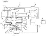
- FIG. 1 is a configuration diagram of an apparatus used in Embodiment 1.
- FIG. The figure which shows the method for acquiring a secondary electron selectively under atmospheric pressure. Simulation results showing the relationship between electron energy and mean free process in atmospheric pressure space.
- substrate current image which shows the relationship between an electric field and sample GAP when the imaging method of Example 1 is used.
- FIG. 10 is a diagram illustrating an example of a circuit configuration for removing a leakage current component according to the third embodiment.
- FIG. 10 is a diagram illustrating an example of an environmental cell holder type secondary electron detection configuration according to a fourth embodiment.
- FIG. 10 shows an example of a method for measuring a sample GAP using an optical microscope in Example 5.
- FIG. 10 is a diagram illustrating an example of a method for electrically measuring a sample GAP in the fifth embodiment.
- an electric field for amplifying secondary electrons is formed between the partition wall and the sample, and the distance between the partition wall and the sample is set to a distance that is not affected by the amplification by scattering of the reflected electrons.
- a scanning electron microscope SEM
- SEM scanning electron microscope
- the present invention can also be applied to a scanning ion microscope, a scanning transmission electron microscope, a combined device of these and a sample processing device, or an analysis / inspection device using these.
- atmospheric pressure means an atmospheric atmosphere or a predetermined gas atmosphere, and means an atmospheric pressure or a pressure environment of the same level. Specifically, it is about 10 ⁇ 5 Pa (atmospheric pressure) to about 10 ⁇ 3 Pa.
- partition wall means that the non-vacuum space in the sample chamber and the vacuum space in the electron optical column are separated to maintain the pressure difference between them, and the charged particle beam can pass or pass through.
- it means an orifice, a thin film, or a member including these.
- a thin film used as a partition wall is referred to as a “diaphragm”, and in the following, an example in which a non-vacuum space and a vacuum space are separated using a diaphragm will be described. Is also possible.
- FIG. 1 shows the configuration of the scanning electron microscope of this example.
- the scanning electron microscope mainly includes an electron optical system, a stage mechanism system, an SEM control system, a signal processing system, and an SEM operation system.
- the electron optical system includes an electron beam source 1 that generates an electron beam, the generated electron beam is focused and guided to the lower part of the electron optical column 2, an optical lens 7 that focuses the sample as a primary electron beam, and scans the primary electrons. It is comprised by elements, such as the deflector 6, and these are stored in the electron optical lens barrel 2.
- FIG. A detector 8 for detecting emitted electrons obtained by the irradiation of the primary electron beam is disposed at the end of the electron beam optical column 2.
- the detector 8 may be outside or inside the electron beam optical column 2.
- the electron optical column 2 may include other lenses, electrodes, and detectors, or some of them may be different from the above, and the configuration of the electron optical system included in the electron beam optical column 2 Is not limited to this.
- the stage mechanism system includes a sample holder 5 on which a sample is placed, a stage 9 that can move in the XYZ axial directions, and an insulator 101 that insulates the sample holder 5 from other members.
- the sample holder 5 may be configured to be able to apply a voltage, and in this case, the sample holder 5 also functions as the lower electrode 33.
- the distance between the diaphragm holding member 35 (upper electrode 32) holding the diaphragm 31 and the sample holder 5 (lower electrode 33) can be adjusted by moving the stage 9 in the Z direction.
- the stage 9 may be tiltable.
- the distance between the diaphragm holding member and the sample holder can be read as the distance between the diaphragm and the sample or the sample GAP.
- the sample GAP is adjusted using the stage 9, but the diaphragm unit 30 itself has a structure that can move in the Z direction, and the sample GAP is adjusted by moving the partition unit 30. Also good.
- a mechanism for adjusting the sample GAP is referred to as a sample GAP adjustment mechanism.
- the SEM control system includes an acceleration voltage control unit 10, a deflection signal control unit 11, an electron lens control unit 12, an XYZ stage control unit 13, an exhaust system control unit 16, and a voltage application control unit 21.
- the acceleration voltage control unit 10 controls the acceleration voltage of the primary electron beam by controlling each component of the electron optical system.
- the deflection signal control unit 11 controls the deflector 6 to control the deflection amount of the primary electron beam so that the primary electron beam scans and irradiates the sample.
- the electronic lens control unit 12 controls other electronic lenses and electrodes.
- the XYZ stage control unit 13 controls the movement amount of the stage 9 according to a user instruction or automatically.
- the exhaust system control unit 16 controls the operation of the vacuum pump, and controls the degree of vacuum inside the electron optical column 2, inside the first housing 3, and inside the second housing 4.
- the voltage application control unit 21 applies power to the diaphragm holding member 35 (upper electrode 32) or the sample holder 5 (lower electrode 33) by controlling a power source capable of applying a voltage thereto.
- the voltage can be controlled. That is, in this embodiment, the diaphragm holding member 35 functions as the upper electrode 32, and the sample holder 5 functions as the lower electrode 33. It is desirable that a voltage having both positive and negative polarities can be applied to the upper electrode 32 or the lower electrode 33.
- the voltage application control unit 21 may be a variable voltage power supply.
- the signal processing system includes a detection signal control unit 14, an image forming unit 15, and a current / voltage conversion unit 19.
- the detection signal control unit 14 performs a current-voltage conversion process on the signal from the detector 8 and outputs it to the image forming unit.
- the image forming unit 15 generates an image based on the signal output from the detector and the information on the electron beam irradiation position from the deflection signal control unit 11.
- the current-voltage converter 19 is connected to at least the sample holder 5 (lower electrode 33), converts the current detected at least one of the lower electrodes 33 into a voltage signal, and outputs the voltage signal to the image forming unit 15.
- the current-voltage converter 19 is connected to both the upper electrode 32 and the lower electrode 33, and may be switchable so that the current in either one can be detected, or the current can be detected in both. There may be.
- the SEM operation system includes an operation unit 17 that operates each unit control system, and a display unit 18 such as a monitor that displays control values and images processed by the image forming unit.
- control unit and the image generation unit described above may be configured as hardware by a dedicated circuit board, or may be configured by software executed by a computer connected to the charged particle microscope.
- hardware When configured by hardware, it can be realized by integrating a plurality of arithmetic units for executing processing on a wiring board or in a semiconductor chip or package.
- software When configured by software, it can be realized by mounting a high-speed general-purpose CPU on a computer and executing a program for executing desired arithmetic processing. It is also possible to upgrade an existing apparatus with a recording medium in which this program is recorded.
- These devices, circuits, and computers are connected by a wired or wireless network, and data is transmitted and received as appropriate.
- the electron optical column 2 is provided so as to protrude into the first housing 3.
- the first casing 3 communicates with the inside of the electron optical barrel 2 through the hole of the magnetic pole of the objective lens at the end of the electron optical barrel, and has a structure for supporting the electron optical barrel 2. Moreover, it connects with the vacuum pump 28 and an exhaust pipe, and the inside of the 1st housing 3 is maintained in a vacuum state.
- the air pressure inside the first housing 3 may be a vacuum degree equivalent to that inside the electron optical column, or may be lower than the vacuum degree of the electron optical column.
- the sample is placed inside the second housing 4 (also referred to as sample chamber).
- the second casing 4 is provided to support the first casing 3 below the first casing, but the arrangement is not limited thereto.
- the inside of the second casing 4 is non-vacuum, that is, an air atmosphere or a predetermined gas atmosphere.
- the second casing may be open to the atmosphere through the opening.
- the inside of the electron optical column 2 that is vacuum and the inside of the first housing 3 and the inside of the second housing 4 that is non-vacuum are partitioned by a partition wall (for example, a diaphragm unit 30).
- the diaphragm unit 30 is provided on the lower surface of the first housing 3 at a position directly below the electron beam optical barrel 2.
- the partition unit 30 includes a diaphragm 31, a base 34 on which the diaphragm 31 is formed, and a diaphragm holding member 35 that holds the base 34.
- the diaphragm 31 can transmit or pass the primary electron beam emitted from the lower end of the electron optical column 2 and has a differential pressure between the inside of the first housing that is vacuum and the inside of the second housing that is non-vacuum. It must be possible to maintain
- the material of the diaphragm 31 is a carbon material, an organic material, a metal material, silicon nitride, silicon carbide, silicon oxide, or the like.
- the thickness of the diaphragm 31 is preferably a thickness that allows primary electrons and reflected electrons to pass therethrough. Although the thickness depends on the window size and material of the diaphragm 31, a thickness of about 20 nm can be used.
- the diaphragm 31 may be a plurality of windows arranged.
- the shape of the diaphragm 31 is not square but may be a rectangle or the like. Any shape may be used. Further, the conductivity of the diaphragm 31 itself does not matter.
- the diaphragm unit 30 having a SiN film having a film thickness of 20 ⁇ m and a window size of 250 ⁇ m is used. However, the present technology is not limited by the diaphragm size.
- the base 34 is a member such as silicon or a metal member.
- the diaphragm holding member 35 is a member for attaching the diaphragm 31 and the base 34 so as to partition the first casing 3 and the second casing 4.
- the diaphragm holding member 35 may be configured to be able to apply a voltage as will be described later. In this case, the diaphragm holding member 35 also functions as the upper electrode 32.
- the primary electron beam passes through the diaphragm unit 30 and finally reaches the sample 100 mounted on the sample holder 5 (lower electrode 33).
- the sample 100 is irradiated with the primary electron beam, secondary electrons and reflected electrons are emitted from the sample.
- secondary electrons can be detected as a current flowing into the lower electrode 33 based on the principle described later with reference to FIG.
- a signal from the current-voltage conversion unit 19 connected to the lower electrode 33 is detected in synchronization with the deflector 6 by the image forming unit 15 to form a substrate current image.
- the substrate current image is displayed on the display unit 18 via the operation unit 17.
- the current amount of the lower electrode is the substrate current amount or the lower electrode current image
- the current amount of the lower electrode is measured by the substrate current measurement or the lower electrode current measurement
- the measured substrate current is measured by the control unit.
- the image formed image is expressed as a substrate current image or a lower electrode image.
- the distance between the diaphragm and the sample is referred to as a sample GAP.
- the distance between the diaphragm and the sample refers to the distance between the diaphragm surface and the sample surface or the distance between the diaphragm surface and the sample holder surface.
- the primary electron beam is represented by PE
- the secondary electron is represented by SE
- the reflected electron is represented by BSE
- the electron / ion current resulting from the amplified secondary electron is represented by I.
- the sample is omitted.
- Secondary electrons are amplified by ionizing collision with gas molecules present in the non-vacuum space between the diaphragm 31 and the lower electrode 33. More specifically, positive ions and electrons are generated by ionization collision with gas molecules, and the secondary electrons lose energy. Thereafter, the generated positive ions and electrons collide with different gas molecules, and positive ions and electrons are generated again. This process is repeated to amplify secondary electrons.
- the voltage application control unit 21 forms an electric field in the non-vacuum space between the diaphragm 31 and the lower electrode 33, thereby giving the secondary electrons energy necessary for amplification, and the total number of ionization collisions. It is possible to amplify signal components derived from secondary electrons.
- FIG. 2 shows an example in which current is detected by the lower electrode.
- a positive voltage is applied to the upper electrode by the voltage application control unit 21, but it is considered that positive ions and electrons generated by ionization collision are mixedly absorbed by the lower electrode 33. .
- the reflected electrons are similarly amplified by ionization collision with gas molecules.
- the reflected electrons have sufficiently higher energy than secondary electrons, amplification is repeated by ionization collision when the sample GAP is small. Pass through the diaphragm 31 before. Therefore, by using the sample GAP with no or little ionization collision of reflected electrons, the amplified current due to secondary electrons can be selectively detected.
- the sample GAP can be adjusted by controlling the stage 9.
- sample GAP (x) / average free path of electron ( ⁇ ) average number of scattering times ( ⁇ ), and the average total amplification in sample GAP is as simple as ⁇ e ⁇ (E) x Can be expressed. Based on this relationship, the current amounts of the reflected electrons and secondary electrons amplified by the electric field are simply expressed as follows.
- ⁇ and ⁇ are electron emission rates emitted from the sample when irradiated with the primary electron beam, the electron emission rate of reflected electrons is ⁇ , and the electron emission rate of secondary electrons is ⁇ .
- ⁇ SE and ⁇ BSE are the average number of scattering times
- x is the sample GAP
- ⁇ (E) is the amount of electron amplification that varies with the electric field.
- the range of the electron emission rate is 0.01-0.6 and ⁇ is 0.1-1.
- FIG. 3 shows the relationship between the average free process and the acceleration voltage of the primary electron beam in the atmospheric pressure space, which is obtained from a theoretical formula for the relationship between the mean free process at each acceleration voltage.
- the vertical axis represents the mean free path
- the horizontal axis represents the energy of accelerated electrons. It can be seen that as the acceleration voltage increases, the mean free process amount of electrons also increases. For example, when the acceleration voltage is 10 keV, the mean free process is 20 ⁇ m, when the acceleration voltage is 20 keV, the mean free process is 40 ⁇ m, and when the acceleration voltage is 30 keV, the mean free process is 60 ⁇ m. Since the energy of the reflected electrons is determined by the acceleration voltage of the primary electron beam, the secondary electrons are selectively amplified and detected by adjusting the sample GAP so that ⁇ BSE ⁇ SE according to the acceleration voltage. I can do it.
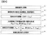
- FIG. 4 shows a flow of acquiring a substrate current image having desired information by selectively detecting emitted electrons.
- the visual field is moved to the observation position of the sample by the stage mechanism system (S1).
- the acceleration voltage and irradiation current which are basic observation conditions, are set using the operation operation of the SEM (S2).
- the sample GAP is adjusted based on the mean free path of the primary electron beam in the gas existing in the non-vacuum space where the sample is placed (S3).
- the acceleration voltage for which the acceleration voltage is set in S2 is used as a parameter.
- the sample GAP is set to be smaller than the mean free path ⁇ PE of the primary electron beam.
- the mean free path may be automatically calculated by simulation or the like from the pressure and type of gas in the sample chamber, or may be obtained by the user.
- the sample GAP may be adjusted by moving the sample in the Z direction by a stage mechanism system. When this step is performed, the sample is irradiated with the primary electron beam.
- an electric field is formed between the upper electrode and the lower electrode by the voltage application control unit 21 (S4).
- the voltage value is adjusted according to whether the desired information is a reflected electron image or a secondary electron image.
- I BSE I SE
- I BSE I SE
- I BSE I SE
- I BSE I SE
- an electric field may be applied to obtain a secondary electron image.
- the applied voltage is increased, the leakage current from the upper electrode to the lower electrode increases as will be described later with reference to FIG. Therefore, it is desirable to set the applied voltage so that the leakage current is smaller than the amount of current caused by the amplified secondary electrons flowing into the substrate.
- Such a value of the applied voltage may be set to a predetermined value in advance.
- the sample GAP is adjusted again (S5). In this step, adjusted to be a ⁇ BSE ⁇ SE. The closer the sample GAP is, the smaller the ⁇ BSE is. Therefore, if the secondary electron image cannot be obtained after the step S4, the sample stage may be brought closer to the diaphragm.
- a current flowing through the substrate through the sample is converted into a signal voltage by the current-voltage conversion unit 19, and the sampled signal voltage is displayed as image data by the image forming unit 15 in synchronization with the deflection signal of the deflection unit 6. Is displayed or stored in the section (S6).
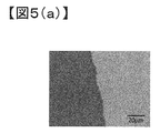
- FIG. 5A is an atmospheric pressure SEM image of the SiC / Au substrate acquired by the backscattered electron detector 8 installed at the lower part of the electron optical column 2. It can be seen that Au has a brighter contrast than the SiC region and is an image caused by reflected electrons.
- FIG. 5B shows the result of verifying the relationship between the electric field formed between the sample and the diaphragm and the sample GAP.
- FIG. 5B compares an example in which the electric field formed between the sample and the diaphragm is no electric field and 100 V / ⁇ m.
- the experimental conditions were an acceleration voltage of 30 kV and an irradiation current of 2 nA, and the substrate current images at no electric field / when an electric field was applied when the sample GAP was 50 ⁇ m, 100 ⁇ m, and 150 ⁇ m were compared.
- the substrate current signal has a contrast obtained by inverting the difference in electron emission rate. Therefore, in FIG. 5B, the substrate current signal is inverted and imaged. If the substrate current image is an image formed by the amplification of reflected electrons, Au is brighter than SiC, and if the image is formed by the amplification of secondary electrons, SiC is brighter. Become.
- the substrate current image is brighter for Au, which has a higher emission rate of reflected electrons, and darker for SiC.
- secondary electrons are not amplified and are reabsorbed by the sample. Since the electrons emitted from the sample are only reflected electrons, a contrast due to the reflected electrons is formed. Moreover, this result became the same tendency in each sample GAP.
- SiC is bright and Au is dark, and the contrast is opposite to the reflected electron image (FIG. 5A). I understood.
- the amplified signal by the secondary electrons is selectively acquired.
- the sample GAP was 50 ⁇ m and 100 ⁇ m when the electric field was 100 V / ⁇ m.
- the amplified signal component derived from the reflected electrons increased with an increase in the average number of scattered electrons. Therefore, the acquired substrate current image becomes close to the reflected electron image. From this result, it was confirmed that the amplification by ionization collision derived from the secondary electron signal can be measured under the condition of the sample gap.
- the sample GAP for which the resolution is guaranteed is preferably x ⁇ 3 ⁇ PE .
- the range of the sample GAP in which secondary electrons can be selectively detected is x ⁇ 3 ⁇ BSE .
- ⁇ BSE means the mean free path of reflected electrons in the gas existing in the non-vacuum space where the sample is placed.
- the value of ⁇ BSE varies depending on the electric field applied between the samples GAP.
- the threshold value is set to 3 times ⁇ BSE , but the actual threshold value depends on the material of the sample and the device configuration.
- the voltage applied to the sample GAP is desirably 3 kV / mm or less, which is an electric breakdown field of air.
- the voltage applied to the upper electrode is 150 V or less when the sample GAP is 50 ⁇ m.
- the emission electrons to be detected can be selectively controlled by adjusting the sample GAP.
- the distance traveled by the emitted electrons is long, reflected electrons with high energy repeat many ionization collisions, so more electrons and ions are generated than secondary electrons, and the substrate current is amplified by reflected electrons. Many of the processed signals are superimposed. That is, in the range of x ⁇ 3 ⁇ BSE , the current image is derived from secondary electrons, and in the range of x ⁇ 3 ⁇ BSE , the current image is rich in reflected electron components.
- an amplification phenomenon due to ionization collision of secondary electrons can be selectively generated, and an image having information due to secondary electrons can be acquired. Become.
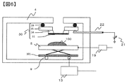
- Fig. 6 shows an outline of the interior of the second housing that holds the sample and the sample stage in the atmosphere.
- the same parts as those in FIG. 1 other than the vicinity of the second housing 4 are omitted, but the same electron beam optical column 2 as that in FIG. Yes.
- the diaphragm holding member 35 functions as the upper electrode 32
- the sample holder 5 functions as the lower electrode 33.
- a voltage is applied to the upper electrode 32 by the voltage application mechanism 22 controlled by the voltage application control unit 21.
- the voltage application mechanism 22 is a metal rod having a leaf spring structure at the tip. A voltage is applied to the upper electrode by contacting the upper electrode through the leaf spring portion.
- the voltage application mechanism 22 is inserted through the insertion portion of the wall surface of the second casing and is connected to the voltage application control unit 21 outside the second housing 4. The voltage application to the voltage application mechanism 22 may be performed from the outside using a terminal on the sample stage 5 side. A terminal connected to the sample holder 5 may be installed in the second housing 4. Further, the voltage application mechanism 22 may be omitted, and the voltage application control unit 21 may be directly wired to the upper electrode 32.
- the current / voltage converter 19 is connected to the lower electrode 33, and the current absorbed by the lower electrode 33 is converted into a voltage and output to the image forming unit 15.
- the sample 100 is placed on the sample holder 5 which is the lower electrode 33.
- a voltage is applied to the upper electrode 32.
- a voltage may be applied to the lower electrode 33.
- the current-voltage converter 19 connected to the lower electrode 33 has a circuit configuration that is electrically floated by the voltage application controller 21, and the upper electrode 32 is grounded.
- the space in which the sample is installed is maintained in an atmospheric state by a sealing material 39 such as an O-ring between the upper electrode 32 and the second housing 4.
- the sample GAP can be adjusted by the Z axis of the stage 9.
- the environment of the second housing 4 is the atmosphere, but the gas inside the second housing may be a gas different from the atmosphere.
- He or Ar may be included.
- He has a smaller element number and density than gas molecules, it has a long mean free path. Therefore, by including He in the gas inside the second casing, the mean free path becomes longer and the adjustment of the sample GAP becomes easier.
- the present invention does not necessarily need to be atmospheric pressure, and the applicable vacuum range is from 1330 Pa to atmospheric pressure. When the pressure decreases, the molecular density in the gas decreases, so the probability that air molecules collide with electrons decreases. Therefore, the mean free path becomes long.
- the sample GAP may be a sample GAP (x ⁇ 3 ⁇ BSE ) within three times the mean free path of reflected electrons.
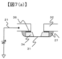
- FIG. 7 is a configuration example for ensuring the conductivity of the upper electrode 32 and the diaphragm 31.
- the diaphragm unit includes a diaphragm 31 that can transmit electrons deposited on a base and an upper electrode 32 that is made of a metal material that fixes the diaphragm.
- the upper electrode 32 has an opening through which the primary electron beam and the reflected electrons pass, and is installed so that the center coincides with the SiN opening of the diaphragm 31.
- the base 34 and the upper electrode 32 on which the diaphragm 31 is formed are fixed using an adhesive 36. At that time, both the opening of the upper electrode 32 and the SiN opening of the diaphragm 31 are made so as not to disturb the primary electron beam and the reflected electrons. It does not matter whether the adhesive 36 has electrical conductivity.
- the conductive material 37 for example, silver paste, carbon paste, or Cu tape can be used. If the base 34 is conductive, the adhesive 36 may also serve as the conductive material 37.
- FIG. 7B shows an example in which the diaphragm 31 and the base 34 are fixed to the upper electrode 32 using the conductive cap 38.
- the base may be attached to the upper electrode 32 with a cap (conductive cap 38) made of a conductive material as shown in FIG. 7B.
- a sealing material 47 such as an O-ring may be provided between the base 34 and the upper electrode 32.
- the conductive cap 38 can be attached to and detached from the diaphragm and the upper electrode. Also in the example of FIG. 7B, as shown in FIG.
- the upper electrode 32 is attached to the second casing 4 via a sealing material 39 such as an O-ring, and the inside of the second casing 4 Is separated from the vacuum space inside the charged particle optical column.
- a sealing material 39 such as an O-ring
- the inside of the second casing 4 Is separated from the vacuum space inside the charged particle optical column.
- FIG. 7A since the diaphragm is fixed to the upper electrode by adhesion, it is necessary to replace the upper electrode together with the diaphragm.
- a removable conductive cap as shown in FIG. 7B, it is not necessary to replace the upper electrode itself, which is a diaphragm holding member, when replacing the diaphragm.
- the diaphragm 31 and the base 34 can be removed from the upper electrode and exchanged. Therefore, the upper electrode can be reused.
- the present embodiment it is possible to selectively acquire secondary electrons under atmospheric pressure by the voltage application mechanism.
- secondary electrons When secondary electrons are detected by the upper electrode, reflected electrons also enter the upper electrode in the same manner, so that it is difficult to discriminate and detect secondary electrons and reflected electrons.
- the method of detecting secondary electrons amplified by measuring the substrate current with the lower electrode as in the present embodiment the electric field formed between the sample GAP and the magnitude of the sample GAP. Thus, it is possible to discriminate and detect secondary electrons and reflected electrons.
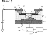
- FIG. 8A shows a sample holder configuration for reducing leakage current.
- An insulating member 40 is installed between the diaphragm 31 and the sample 100. According to another expression, the insulating member 40 is placed on the surface of the diaphragm 31 so as to face the sample. Note that a hole is provided in the central portion of the insulating material (opening portion of the base 34) so that the primary electron beam and the reflected electrons can pass therethrough.
- the insulating member 40 is installed on the outer periphery of the diaphragm 31 so as not to overlap the SiN opening of the diaphragm 31. As a result, the resistance between the upper electrode 32 and the lower electrode 33 is increased, and the leakage current flowing through the lower electrode 33 is reduced.
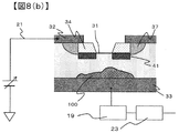
- the insulating member 40 used at this time may be a cellophane tape or a polyimide tape. Further, as shown in FIG. 8B, a film in which an insulating film 41 such as a resist or a PIQ film is formed on the diaphragm 31 itself may be used.
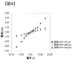
- FIG. 9 shows an actual measurement result of the leakage current to the lower electrode 33 when a voltage is applied to the upper electrode 32.
- FIG. 9 shows measurement results in a state where one layer of a polyimide tape having a thickness of 50 ⁇ m is attached to the diaphragm holder 30 as shown in FIG. The vertical axis is the leakage current amount, and the horizontal axis is the voltage applied to the upper electrode. From this result, it was found that there was a leakage current that could not be removed by the polyimide tape alone, and the amount of leakage current flowing through the lower electrode 33 was proportional to the applied voltage and the sample GAP.
- the current measurement processing unit 23 is provided for the current signal flowing through the lower electrode.
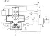
- FIG. 10 shows the overall configuration of the apparatus in this embodiment.
- the current measurement processing unit 23 is an adjustment circuit that measures a leak current and offsets the leak current. It is desirable to measure the amount of leakage current used for offset for each observation. For example, when the sample is replaced, it is desirable to measure again the leakage current used for the offset when the working distance (sample GAP) is changed. In other words, by irradiating the sample with a charged particle beam while an electric field is applied between the upper electrode and the lower electrode, the amount of leakage current used for offset is subtracted from the amount of current flowing into the lower electrode.
- the offset measurement is performed by subtracting the leakage current amount set every time (that is, every pixel) from the current flowing into the lower electrode 33 by the current measurement processing unit 23.
- the current signal is output to the image forming unit 15 and an image is formed.
- a method for measuring leakage current as an offset will be described.
- a voltage is applied from the voltage application control unit 21 to the upper electrode 32 without irradiating the primary electron beam to generate an electric field.
- the value is measured.
- the actually measured leakage current amount is input and stored in the current measurement processing unit 23 as an offset for measuring the lower electrode current.
- the correctable electric field range is desirably up to 1 V / ⁇ m.
- FIG. 11 shows a specific example of the offset adjustment circuit used as the current measurement processing unit 23.
- This circuit is an example, and it is sufficient that offset adjustment is possible and a signal amplifier circuit is provided.
- This circuit may be installed either inside the second housing or outside the second housing.
- an SEM configuration will be described in which a capsule-like sample cell is placed in a vacuum-evacuated casing and secondary electrons from a sample under atmospheric pressure can be selected and detected.
- This sample cell has a space in which a sample can be placed, and the inside of the sample cell can be in an atmosphere of any gas type and pressure. In this embodiment, the inside of the sample cell is the atmosphere.
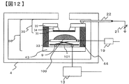
- FIG. 12 shows a schematic diagram of the inside of the second housing 4 in which the sample cell is installed. Since the outside of the second housing is the same as that of FIG.
- the sample cell 50 includes an upper electrode 32, a lower electrode 33, and a sealing material 44.
- the sealing material 44 forms the side wall of the sample cell 50, seals the upper electrode 32 and the lower electrode 33, and maintains an atmospheric pressure space in the vacuum space.
- a diaphragm unit 30 is attached to the upper electrode.
- the upper electrode 32 functions as a lid for the sample cell.
- the sample 100 is disposed on the lower electrode inside the sample cell. That is, it is installed between the upper electrode 32 and the diaphragm unit 30 and the lower electrode 33.
- the voltage application mechanism 22 controlled by the voltage application control unit 21 is installed so as to be in contact with the upper electrode 32, and applies a voltage to the upper electrode 32.
- a voltage may be applied to the lower electrode 33 instead of applying a voltage to the upper electrode 32.
- the current / voltage converter 19 is connected to the lower electrode 33.
- the sealing material 44 between the lower electrode 33 and the upper electrode 32 must maintain an atmospheric pressure space and be electrically separated.
- an insulating material that does not conduct electricity is used for at least a part of the sealing material 44.
- the insulating material may be, for example, an O-ring, a gel sheet, or an adhesive.
- the sealing material 44 itself may be made of an insulating material. Further, this insulating material may be used as a spacer for securing or adjusting the sample GAP.
- the height of the sealing material 44 may be changed or may be changed by using a stage mechanism provided in the sample cell.
- the operation of the stage mechanism is controlled by an XYZ stage controller that can move in the XYZ directions.
- an XYZ stage 9 is installed in the capsule.
- the stage is electrically insulated from the lower electrode 33 by the insulator 101.
- a voltage can be applied between the upper electrode 32 and the lower electrode 33, and the sample GAP between the sample 100 and the diaphragm 31 can be adjusted. Therefore, it is possible to acquire a secondary electron image in a state where the sample is installed under atmospheric pressure even in a vacuum evacuated casing.
- control of the sample GAP is important when implementing the present invention.
- the sample GAP can be narrowed by accurately measuring the height of the sample GAP. Thereby, since the scattering of primary electrons can be reduced under atmospheric pressure, the resolution is improved. Further, since the signal component corresponding to the amplification of ionization scattering by the reflected electrons is reduced, the selectivity of secondary electrons is improved, and the contrast reflecting the surface shape can be obtained more clearly in the base current image.
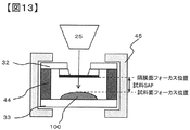
- FIG. 13 shows a schematic diagram of sample GAP measurement using an optical microscope.
- the upper electrode 32, the sealing material 44, and the lower electrode 33 are fixed so as to be sandwiched by the fixing jig 45, thereby creating a sealed space.
- the sample 100 is set so that the observed portion is directly below the SiN opening.
- the XYZ stage 9 is built in the holder, the XYZ stage may be adjusted so that the part to be observed of the sample is directly below.
- an optical microscope is used to adjust the focus position on the sample surface and the SiN diaphragm surface, and the difference in focus position between the sample surface and the diaphragm surface is measured. This difference is used as the sample GAP.
- the method for adjusting the sample GAP may be to adjust the sample GAP by selecting and using a plurality of types of sealing materials 44 having different thicknesses, or by adjusting the fixing force of the fixing jig portion 45. You may adjust 44 in the range of squashing.
- the method of FIG. 13 is effective when an environmental cell type holder as shown in FIG. 12 is used.
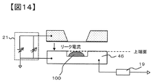
- FIG. 14 shows a method of measuring the sample GAP using the leak current as another example.
- the surface of the observed sample 100 is placed with respect to the upper end surface on the height-adjusting sample stage 46 having a structure in which the portion where the sample 100 is placed is one step lower than the upper end.
- the upper end surface of the height adjustment sample stage 46 and the surface of the sample 100 may be aligned with reference to a focus point of an optical microscope or the like.
- a standard applied voltage is applied from the voltage application control unit 21, and a leak current flowing at that time is measured.
- the sample GAP is obtained from the magnitude of the measured leakage current based on the relationship between the leakage current obtained in advance and the sample GAP.
- the standard applied voltage is constant for each apparatus and is set in advance.
- the relationship between the leakage current and the sample GAP is measured in advance and stored in a database or the like.
- FIG. 15 shows another example of a method for measuring a sample GAP in a scanning electron microscope using electrons.
- the amount of flare increases due to collision with gas molecules, and the beam diameter increases before reaching the sample.
- the beam diameter In vacuum, since there are almost no gas molecules, the beam diameter has almost no flare.
- the sample GAP can be measured by using the flare amount as a parameter.
- a sample made of a heavy metal system such as Au, Cu, or Pt on a thin film placed on Si or Al is used as a standard sample for sample GAP measurement.
- the standard sample is installed at an arbitrary position of the sample holder 5.
- FIG. 15 (a) shows a schematic diagram of a display unit obtained by acquiring the flare amount measurement sample in a vacuum.
- FIG. 15B is a model diagram of an SEM obtained by acquiring a flare amount measurement sample in the atmosphere.
- the display unit 18 and the operation unit 17 input the type, pressure, acceleration voltage, and temperature of the gas molecules in the measurement environment to the user, and the flare amount is obtained by simulation from these parameters. Or you may memorize
- 15 (a) and 15 (b) show an example of screen display for explanation, but the screen display may not be performed if the flare amount is automatically obtained by image processing.
- the sample GAP is obtained from the acquired flare amount by comparing or collating the actually measured flare amount and the flare amount calculated by the simulation by the image processing unit.
- the relationship between the flare amount and the sample GAP may be obtained by simulation or may be obtained by a predetermined relational expression.
- data on the relationship between the flare amount and the sample GAP may be stored in advance, and the sample GAP may be obtained by collating with the data.
- the sample GAP can be measured, so that a substrate current image with high resolution and high secondary electron selectivity can be obtained.
- FIG. 16 shows an operation GUI which is a user interface used in this embodiment.
- the operation GUI shown in FIG. 16 is displayed on the display unit 18.
- Data is input by a mouse or a keyboard connected to the operation unit 17.
- the screen of FIG. 16 may be automatically activated, or the observation conditions may be automatically set as default values.
- the acceleration voltage may be set as a default value.
- the type of gas in the sample chamber when the gas type button 29 is clicked for observation is selected, and the pressure of the gas is input.
- the mean free path is calculated in advance according to the acceleration voltage and stored as a database on the hard disk or memory.
- the operation unit 17 obtains an average free process according to the acceleration voltage set in the measurement condition. Therefore, the mean free process does not need to be calculated by the user, and is automatically set by inputting the gas information in the sample chamber.
- the observation condition setting screen has an applied voltage input window 25, and the user inputs a voltage to be applied to the upper electrode or the lower electrode to the applied voltage input window 25. The voltage of the input value is applied.
- the observation condition setting screen may have a leakage current measurement button 26.
- the user can measure the substrate current detected by the lower electrode by clicking the leak current measurement button 26. Therefore, the leakage current can be measured by pressing the leakage current measurement button under the conditions described in the above embodiment. Further, when the offset button 27 is clicked, the measured leakage current is set as the offset of the substrate current detected by the lower electrode as described in the above-described embodiment.
- this invention is not limited to the above-mentioned Example, Various modifications are included.
- the above-described embodiments have been described in detail for easy understanding of the present invention, and are not necessarily limited to those having all the configurations described.
- a part of the configuration of one embodiment can be replaced with the configuration of another embodiment, and the configuration of another embodiment can be added to the configuration of one embodiment.
- Each of the above-described configurations, functions, processing units, processing means, and the like may be realized by hardware by designing a part or all of them with, for example, an integrated circuit.
- Each of the above-described configurations, functions, and the like may be realized by software by interpreting and executing a program that realizes each function by the processor.
- Information such as programs, tables, and files for realizing each function can be stored in a recording device such as a memory, a hard disk, an SSD (Solid State Drive), or a recording medium such as an IC card, an SD card, or an optical disk.
- a recording device such as a memory, a hard disk, an SSD (Solid State Drive), or a recording medium such as an IC card, an SD card, or an optical disk.
- control lines and information lines indicate what is considered necessary for the explanation, and not all the control lines and information lines on the product are necessarily shown. Actually, it may be considered that almost all the components are connected to each other.
Landscapes
- Chemical & Material Sciences (AREA)
- Analytical Chemistry (AREA)
- Analysing Materials By The Use Of Radiation (AREA)
Abstract
本発明は、大気中で二次電子像観察が可能な電子顕微鏡および観察手法を提供する。 より具体的には、本発明の荷電粒子顕微鏡は、荷電粒子光学鏡筒(2)内部の真空空間から試料が載置される非真空空間を分離する隔壁(31)と、上部電極(35)と、試料(100)が載置される下部電極(5)と、上部電極または下部電極の少なくともいずれか一方に電圧を印加する電源(21)と、試料と前記隔壁の間隔を調整する試料ギャップ調整機構(9)と、下部電極に吸収された電流に基づいて前記試料の画像を形成する画像形成部(15)と、を有する。上部電極と下部電極の間に電圧を印加した際に発生する気体分子と電子の電離衝突による増幅効果を利用して二次電子を選択的に計測する。検出方式は下部電極に流れた電流値を計測する手法を用いる。
Description
本発明は、荷電粒子線を利用して試料の画像を取得する荷電粒子顕微鏡に関する。
顕微鏡の中でも、光源に電子を利用した電子顕微鏡はnmオーダーでの表面形状の観察が可能である。その中でも、走査型電子顕微鏡(以下、SEM)は、微細な表面形状の観察や組成構造の観察に広く使用されている。SEMは、電子レンズによって試料表面に集束した電子線(一次電子線)を偏向器によって走査し、試料の電子線が照射された領域から発生した放出電子を検出して、画像化する装置である。放出電子には、表面形状の情報を有する低エネルギの放出電子(以下、二次電子という)、および一次電子線と同程度のエネルギを有し、組成情報を有する後方散乱電子(以下、反射電子という)が含まれる。
ソフトマテリアルや生物試料を観察する場合には、形状変形や水分蒸発が発生しない大気圧下での高分解能観察が望まれている。しかし、電子線は気体分子との衝突によって散乱されるため、大気圧下では分解能が低下してしまう。そのため、電子レンズや偏向器などの電子光学系を構成する鏡筒は真空排気されている。通常、SEMでは、鏡筒と試料を設置する筐体とを真空排気するため、試料は真空下に配置されることになる。このような理由から電子顕微鏡は含水した試料や気圧変化により形態が変化する試料の観察には不向きであった。
近年、真空保持が必要な電子光学系を構成する鏡筒と試料を設置する筐体の間に電子線が透過可能な隔膜や微小穴を設け、所望の気圧下に試料を保持し、観察を可能にしたSEMが実用化されている。これにより、大気下や所望のガス圧下またはガス種下で試料を観察することが可能となった。鏡筒と筐体を分離する隔膜を試料に接触させずに電子線を照射する方式を隔膜非接触型と呼ぶ。隔膜非接触型の装置では、試料と隔膜との間に非真空の空間を有しており、一次電子線は当該非真空空間を通過し試料に照射される。さらに、試料からの放出電子のうち、気体による散乱の影響が少ない高いエネルギを有する反射電子が、試料と隔膜との間の非真空空間および隔膜を透過し、鏡筒内に設置した検出器によって検出される。
特許文献1は、隔壁非接触型の走査電子顕微鏡が開示されている。特許文献1の走査電子顕微鏡は、鏡筒と筐体を分離する隔膜と試料との間に、円盤型カソード電極を有し、当該電極と試料間に電界を形成して、放出電子を増幅させ、当該電極経由で放出電子を検出する機構を有している。
走査電子顕微鏡の利点として、二次電子を検出することで試料の表面像を取得することができる点がある。しかしながら、二次電子のエネルギが低いため、大気下や所望のガス圧下またはガス種下で試料を観察可能な電子顕微鏡においては、二次電子は試料室内の気体分子によって散乱され、さらに隔膜を透過できず、検出することが困難であった。
また、特許文献1では、検出電極が試料の直上に設置されているため、電界によって増幅された二次電子の信号に加え、反射電子も検出されてしまう。したがって、二次電子を反射電子と弁別して取得して、表面形状情報を主コントラストとする画像を取得することは困難であった。
本発明では、大気下や所望のガス圧下またはガス種下で試料を観察可能な電子顕微鏡において、表面形状情報を主コントラストとする画像を取得することを目的とする。
上記課題を解決するために、本発明の荷電粒子顕微鏡は、荷電粒子光学鏡筒内部の真空空間から試料が載置される非真空空間を分離する隔壁と、上部電極と、試料が載置される下部電極と、上部電極または下部電極の少なくともいずれか一方に電圧を印加する電源と、試料と前記隔壁の間隔を調整する試料ギャップ調整機構と、下部電極に吸収された電流に基づいて前記試料の画像を形成する画像形成部と、を有する。上部電極と下部電極の間に電圧を印加した際に発生する気体分子と電子の電離衝突による増幅効果を利用して二次電子を選択的に計測する。検出方式は基板に流れた電流値を計測する手法を用いる。
本発明によれば、一次電子の走査に同期して、上部電極または下部電極に吸収された電流を測定することにより、大気下や所望のガス圧下またはガス種下で試料を観察可能な電子顕微鏡において、表面形状情報を主コントラストとする画像を取得することができる。
上記した以外の課題、構成及び効果は、以下の実施形態の説明により明らかにされる。
本発明では、隔壁と試料との間に二次電子を増幅させる電界を形成し、かつ、隔壁と試料との間の距離を反射電子の散乱による増幅が影響しない距離にすることで、選択的に二次電子信号を検出する。
以下、図面を参照し、本発明の実施例について詳細に説明する。
以下では、荷電粒子顕微鏡の一例として、走査電子顕微鏡(SEM)について説明する。ただし、これは本発明の単なる一例であって、本発明は以下説明する実施の形態に限定されるものではない。例えば走査イオン顕微鏡や走査透過電子顕微鏡、これらと試料加工装置との複合装置、またはこれらを応用した解析・検査装置にも適用可能である。
また、本明細書において「大気圧」とは大気雰囲気または所定のガス雰囲気であって、大気圧またはこれと同程度の圧力環境のことを意味する。具体的には約10^5Pa(大気圧)から~約10^3Pa程度である。
また、本明細書において「隔壁」とは、試料室内の非真空空間と電子光学鏡筒内の真空空間とを分離することで両者の気圧差を保持し、かつ荷電粒子線が透過又は通過可能な構造をいう。例えばオリフィスや薄膜、またはこれらを含む部材を意味する。なお、隔壁として用いられる薄膜を「隔膜」と称することとし、以下では隔膜を用いて非真空空間と真空空間を区切る実施例を説明するが、本発明の適用に際しては隔膜を小孔に置き換えることも可能である。
図1に、本実施例の走査型電子顕微鏡の構成を示す。走査型電子顕微鏡は、主に電子光学系と、ステージ機構系と、SEM制御系と、信号処理系と、SEM操作系により構成される。
電子光学系は、電子線を発生する電子線源1、発生した電子線を集束して電子光学鏡筒2の下部へ導き、一次電子線として試料を集束する光学レンズ7、一次電子を走査する偏向器6などの要素により構成され、これらは電子光学鏡筒2に格納されている。電子線光学鏡筒2の端部には、上記一次電子線の照射により得られる放出電子を検出する検出器8が配置される。検出器8は電子線光学鏡筒2の外部にあっても内部にあってもよい。電子光学鏡筒2には、これ以外に他のレンズや電極、検出器を含んでもよいし、一部が上記と異なっていてもよく、電子線光学鏡筒2に含まれる電子光学系の構成はこれに限られない。
ステージ機構系は、試料を載置する試料ホルダ5と、XYZ軸方向に移動可能なステージ9、試料ホルダ5をその他の部材と絶縁する絶縁体101とを含んで構成される。試料ホルダ5は後述するように電圧印加可能な構成となっていてもよく、その場合には下部電極33としても機能する。隔膜31が保持された隔膜保持部材35(上部電極32)と試料ホルダ5(下部電極33)の距離を、ステージ9のZ方向の移動によって調整することが可能である。またステージ9は傾斜可能であってもよい。なお、隔膜保持部材と試料ホルダの距離は、隔膜と試料との距離、または試料GAPと読み替えることもできる。本実施例では、ステージ9を用いて試料GAPを調整しているが、隔膜ユニット30自体がZ方向に移動可能な構造を有しており、隔壁ユニット30を動かすことで試料GAPを調整してもよい。試料GAPを調整する機構を試料GAP調整機構と称する。
SEM制御系は、加速電圧制御部10と、偏向信号制御部11と、電子レンズ制御部12と、XYZステージ制御部13と、排気系制御部16、電圧印加制御部21とを含んで構成される。加速電圧制御部10は、電子光学系の各部品を制御することで一次電子線の加速電圧を制御する。偏向信号制御部11は、偏向器6を制御して一次電子線が試料上を走査照射するように一次電子線の偏向量を制御する。電子レンズ制御部12はその他の電子レンズや電極を制御する。XYZステージ制御部13は、ユーザの指示によりまたは自動的にステージ9の移動量を制御する。排気系制御部16は、真空ポンプの動作を制御し、電子光学鏡筒2の内部、第一筺体3の内部および第二筺体4の内部の真空度を制御する。電圧印加制御部21は、後述するように隔膜保持部材35(上部電極32)または試料ホルダ5(下部電極33)の少なくともいずれか一方に電圧が印加可能な電源を制御することによりこれらに印加する電圧を制御することができる。つまり、本実施例では隔膜保持部材35が上部電極32として機能し、試料ホルダ5が下部電極33として機能する。上部電極32または下部電極33には、正負両方の極性の電圧を印加できることが望ましい。これによって試料と隔膜との間の空間(試料GAP)に所望の電界を形成することができる。また、上部電極32、下部電極33は、それぞれ隔膜保持部材、試料ホルダとは別個に設けられてもよい。電圧印加制御部21は可変電圧電源であってもよい。
信号処理系は、検出信号制御部14、画像形成部15、電流電圧変換部19を含んで構成される。検出信号制御部14は検出器8からの信号を電流-電圧変換する処理を行い、画像形成部に出力する。画像形成部15は検出器から出力される信号と、偏向信号制御部11からの電子線照射位置の情報に基づいて画像を生成する。電流電圧変換部19は、隔少なくとも試料ホルダ5(下部電極33)に接続され、下部電極33の少なくとも一方で検出される電流を電圧信号に変換して画像形成部15に出力する。電流電圧変換部19は、上部電極32および下部電極33の両方に接続されていて、どちらか一方における電流を検出できるように切替可能であってもよいし、両方でそれぞれ電流を検出できる構成であってもよい。
SEM操作系は、各部制御系を操作するオペレーション部17と、制御値や画像形成部で処理した画像を表示するモニタ等の表示部18とを含んで構成される。
上記した制御部や画像生成部は、専用の回路基板によってハードウェアとして構成されていてもよいし、荷電粒子顕微鏡に接続されたコンピュータで実行されるソフトウェアによって構成されてもよい。ハードウェアにより構成する場合には、処理を実行する複数の演算器を配線基板上、または半導体チップまたはパッケージ内に集積することにより実現できる。ソフトウェアにより構成する場合には、コンピュータに高速な汎用CPUを搭載して、所望の演算処理を実行するプログラムを実行することで実現できる。このプログラムが記録された記録媒体により、既存の装置をアップグレードすることも可能である。また、これらの装置や回路、コンピュータ間は有線又は無線のネットワークで接続され、適宜データが送受信される。
電子光学鏡筒2は第一筺体3の内部に突出するように設けられている。第一筺体3は、電子光学鏡筒端部の対物レンズの磁極の穴を通して電子光学鏡筒2の内部と連通しており、電子光学鏡筒2を支持する構造となっている。また、真空ポンプ28と排気管によって接続され、第一筺体3の内部は真空状態に維持される。第一筺体3の内部の気圧は電子光学鏡筒の内部と同等の真空度であってもよいし、電子光学鏡筒の真空度よりは低真空となっていてもよい。
試料は第二筺体4(試料室ともいう)の内部に配置される。図1の例では、第二筺体4は第一筺体の下部に第一筺体3を支持するように設けられているが、配置はこれに限られない。第二筺体4の内部は非真空、つまり大気雰囲気または所定のガス雰囲気になっている。第二筺体4の内部が大気である場合には第二筺体は開口部を通じて大気開放されていてもよい。また第二筺体4の内部を所定の圧力のガス雰囲気にする場合にはガス導入口が設けられているとよい。また、必要に応じて第二筺体4の内部を真空状態にするには、第二筺体4に真空ポンプに接続可能な排気ポートを設けることが好ましい。
真空である電子光学鏡筒2の内部および第一筺体3の内部と、非真空である第二筺体4の内部は、隔壁(例えば隔膜ユニット30)によって仕切られている。隔膜ユニット30は、第一筺体3の下面で、上記電子線光学鏡筒2の直下になる位置に設けられている。隔壁ユニット30は、隔膜31、隔膜31が成膜された土台34、土台34を保持する隔膜保持部材35から構成される。隔膜31は、電子光学鏡筒2の下端から放出される一次電子線を透過または通過させることが可能であり、かつ、真空である第一筺体内部と非真空である第二筺体内部の差圧を維持可能なものである必要がある。隔膜31の素材はカーボン材、有機材、金属材、シリコンナイトライド、シリコンカーバイド、酸化シリコンなどである。隔膜31の厚みは一次電子及び反射電子が透過可能な膜厚であることが望ましい。厚さは隔膜31の窓サイズや材料によるが約20nmのものを使用することが可能である。隔膜31は複数配置された多窓であってもよい。隔膜31の形状は正方形でなく、長方形などのような形状でもよい。形状に関してはどのような形状でもかまわない。また、隔膜31自体の導電性は問わない。以下で説明する本実施例においては、一例として、膜厚20μm 、窓サイズ250μm のSiN膜が付いた隔膜ユニット30を使用したが、本技術は隔膜サイズにより制約されるものではない。
土台34は例えばシリコンや金属部材のような部材である。隔膜保持部材35は隔膜31および土台34を第一筺体3と第二筺体4の間を仕切るように取り付ける部材である。隔膜保持部材35には後述するように電圧印加可能な構成となっていてもよく、その場合には上部電極32としても機能する。
一次電子線は、隔膜ユニット30を通って最終的に試料ホルダ5(下部電極33)に搭載された試料100に到達する。試料100に一次電子線が照射されると二次電子および反射電子が試料から放出される。図2を用いて後述する原理により、本実施例では、二次電子を下部電極33に流れ込む電流として検出可能である。下部電極33に接続された電流電圧変換部19からの信号は、画像形成部15で偏向器6に同期して検出され、基板電流像が形成される。基板電流像は、オペレーション部17を介し、表示部18に表示される。
以下では、図1に説明した装置を用いて、大気圧空間に試料が設置された状態で二次電子を選択的に検出する方法について述べる。
以下、本明細書において、下部電極の電流量を基板電流量もしくは下部電極電流像、下部電極の電流量を測定することを基板電流計測もしくは下部電極電流計測、計測した基板電流を制御部にて画像形成した像を基板電流像もしくは下部電極像と表現する。また、本明細書では、隔膜-試料間の距離を試料GAPと呼ぶ。なお、ここで隔膜‐試料間の距離とは、隔膜表面と試料表面との距離または隔膜表面と試料ホルダ表面の距離を指す。
大気圧中にはたくさんの気体分子が存在しており、エネルギを有する1つの電子が気体分子に対して衝突すると、1つの電子と1つのイオンが生成される増幅現象が生じる。無電界の場合、衝突により発生した電子やイオンは消失するが、電界を印加すると衝突により発生した電子やイオンは、なだれ的に増幅する。これは光子に対しても同様の現象が発生する。それらの電子による電離衝突で発生した電子の増幅量はeαxであらわされ、電子の電離衝突が多ければ多いほど増幅量も増加する。本発明者らは、この増幅現象を利用し、エネルギの低い二次電子を選択的に検出する方法を考案した。
図2を用いて、二次電子を増幅して検出する原理を説明する。図2では、一次電子線をPE、二次電子をSE、反射電子をBSE、増幅された二次電子に起因する電子/イオン電流をIと表現している。また、図2では試料を省略して記載している。
一次電子線が試料に照射すると試料表面から二次電子および反射電子が放出される。二次電子は隔膜31と下部電極33の間の非真空空間に存在する気体分子と電離衝突することで増幅される。より具体的には、気体分子との電離衝突により、プラスイオンと電子が生成され、二次電子はエネルギを失う。その後生成されたプラスイオンと電子がそれぞれ別の気体分子と衝突し再度それぞれプラスイオンと電子が生成される。この過程が繰り返されて二次電子が増幅される。本実施例では、電圧印加制御部21により隔膜31と下部電極33の間の非真空空間に電界を形成することで、二次電子に対して増幅に必要なエネルギを付与し、全電離衝突回数を増やすことで二次電子由来の信号成分の増幅が可能である。
増幅された電子またはイオンは上部電極32または下部電極33により吸収される。図2では下部電極により電流検出する例を示している。図2の場合には、電圧印加制御部21により上部電極にプラス電圧を印加しているが、下部電極33では電離衝突により生成されたプラスイオンと電子とが混在して吸収されると考えられる。
この際、反射電子も同様に、気体分子との電離衝突により増幅されるが、反射電子はエネルギが二次電子に比べて十分高いため、試料GAPが小さい場合には、電離衝突により増幅を繰り返す前に隔膜31を通過する。したがって、反射電子の電離衝突が無いもしくは少ない試料GAPにすることで、二次電子による増幅電流分を選択的に検出できる。試料GAPはステージ9を制御することで調整可能である。
気体分子との衝突回数は試料GAP(x)/電子の平均自由工程(λ)=平均散乱回数(γ)で決定し、試料GAP中で平均の全増幅量はγeα(E)xと簡易的に表すことが出来る。その関係を踏まえ、電界によって増幅された反射電子及び二次電子の電流量を簡易的に表すと以下のようになる。


ここで、η及びδは、一次電子線を照射した際に試料から放出される電子放出率であり、反射電子の電子放出率はη、二次電子の電子放出率はδである。γSE及びγBSEは平均散乱回数、xは試料GAP、α(E)は電界により変化する電子増幅量である。本実施例での電子放出率の範囲は、ηは0.01-0.6、δは0.1-1である。気体分子と電子の衝突により電子の増幅が発生することから、反射電子が無散乱状態で隔膜31を抜け、真空中に到達すれば、γBSE=0となるためIBSEの信号成分が下部電極で検出されない。また、二次電子は1回の空気分子との衝突でエネルギを失うため、二次電子の平均散乱回数γSE=1である。
上記二つの式により、γBSE<γSEとなる条件であれば、下部電極にて二次電子を選択的に検出可能である。なお、実際にはγBSEとγSEが近い場合には電子放出率η、δに依存することになるが、一般にη<δであるため、γBSE<γSEであれば二次電子を選択的に検出可能であると言える。ここで試料GAPを小さくすればγBSEを小さくすることができるため、γBSE<γSEを満たすように試料GAPを調整すればよい。
図3は、各加速電圧での平均自由工程の関係を理論式より求め、大気圧空間中における一次電子線の加速電圧と平均自由工程との関係を示している。縦軸は平均自由工程、横軸は加速電子のエネルギである。加速電圧が高くなるに従い、電子の平均自由工程量も増加していることが分かる。たとえば、加速電圧10keVの時、平均自由工程が20μm、加速電圧20keVの場合は平均自由工程が40μm、加速電圧30keVの場合は平均自由工程が60μmである。反射電子のエネルギは一次電子線の加速電圧によって決まるため、加速電圧に応じて、γBSE<γSEとなるように試料GAPを調整することで、二次電子を選択的に増幅させ、検出することが出来る。
図4に放出電子を選択的に検出し、所望の情報を有する基板電流像の取得フローを示す。まず、ステージ機構系により、試料の観察場所に視野移動する(S1)。基本的な観察条件である加速電圧、照射電流をSEMの操作オペレーションを用いて設定する(S2)。
次に、試料が載置される非真空空間に存在する気体中での一次電子線の平均自由工程に基づき、試料GAPを調整する(S3)。平均自由工程を求めるに際して、S2で加速電圧が設定された加速電圧をパラメータとして用いる。このステップでは、試料GAPが一次電子線の平均自由工程λPEより小さくなるように設定する。平均自由工程は試料室内の気体の圧力および種類からシミュレーション等により自動的に計算されてもよいし、ユーザが求めてもよい。試料GAPはステージ機構系により試料をZ方向に移動させて調整すればよい。このステップを実施すると、試料に一次電子線が照射される状態になる。
次に、電圧印加制御部21により、上部電極と下部電極間に電界を形成する(S4)。この際、所望の情報が反射電子像であるか二次電子像であるかに応じて電圧値を調整する。反射電子像を取得したい場合にはIBSE>ISEとなるように調整する。二次電子像を取得したい場合にはIBSE<ISEとなるように調整する。実際には、図5を用いて説明するように電圧を印加しない場合には反射電子の成分が多い像が得られるので、二次電子像を得たい場合に電界をかければよい。印加電圧を大きくすると図9を用いて後述するように上部電極から下部電極へのリーク電流が大きくなる。したがって、印加電圧は、増幅された二次電子が基板へ流入することによる電流量よりリーク電流が小さくなるように設定することが望ましい。このような印加電圧の値は予め所定値に設定されていてもよい。
この段階で所望の情報が得られない場合、再度、試料GAPを調整する(S5)。このステップでは、γBSE<γSEとなるよう調整する。試料GAPを近づけるほど、γBSEが小さくなるので、S4のステップを実施後に二次電子像が取得できていない場合には試料ステージをさらに隔膜に近づければよい。
試料を介して基板に流れる電流は、電流電圧変換部19により信号電圧に変換され、偏向部6の偏向信号に同期して、サンプリングされた信号電圧は、画像形成部15により、画像データとして表示部に表示または保存される(S6)。
したがって、実際にはS5とS6のステップを繰り返して、画像を見ながら所望の画像が得られるまで試料GAPを調整すればよい。
図5(a)(b)を用いて試料GAPと電界を調整した場合における取得画像の違いについて説明する。本実施例による二次電子の選択性を評価するため、試料はSiC領域とAu領域を有する試験用試料(SiC/Au基板)を使用した。試験用試料にSiC/Auを使用した理由は、SiCとAuは、加速電圧30kVにおいて、反射電子の放出率はSiCよりAuの方が高く、二次電子の放出率はSiCの方が高くなるためである。
図5(a)は、電子光学鏡筒2下部に設置した反射電子検出器8で取得したSiC/Au基板の大気圧SEM像である。Auの方がSiC領域より明るいコントラストであり、反射電子起因の画像であることが判る。
図5(b)に、試料と隔膜との間に形成される電界と試料GAPの関係を検証した結果を示す。図5(b)では、試料と隔膜との間に形成される電界を、無電界と100V/μmとした例を比較している。実験条件は、加速電圧30kV、照射電流2nAとし、試料GAPが50μm、100μm、150μmの場合における無電界時/電界印加時での基板電流像を比較した。基板電流信号は、電子放出率の差を反転したコントラストとなる。よって、図5(b)では、基板電流信号を反転し、画像化した。基板電流像が、反射電子の増幅分で形成されている像であれば、Auの方がSiCより明るくなり、二次電子の増幅分で形成されている像であれば、SiCの方が明るくなる。
図5(b)によると、無電界の場合、基板電流像は反射電子の放出率が高いAuの方が明るく、SiCが暗くなっている。無電界の場合、二次電子は増幅されず、試料に再吸収される。試料から放出される電子は反射電子のみとなるため、反射電子起因のコントラストを形成する。また、この結果は各試料GAPで同じ傾向となった。試料GAPを50μmとして試料GAP間に100V/μmの電界を印加した場合は、SiCが明るく、Auが暗くなっており、反射電子像(図5(a))とコントラストが反対になっていることが分かった。放出した電子のうち下部電極側に戻ってくるのは電離衝突により生成させたプラスイオン成分であるため、基板電流量が増加する。これより、二次電子による増幅信号を選択的に取得していることが分かる。また、電界100V/μmの場合において試料GAPが50μm、100μmでは同様の現象が見られたが、試料GAPを150μmとすると、反射電子の平均散乱回数の増加に伴い、反射電子由来の増幅信号成分が増加するため、取得される基板電流像が反射電子像に近くなる。
この結果より、試料ギャップの条件において二次電子信号由来の電離衝突による増幅分の計測が可能なことを確認した。
この結果より、試料ギャップの条件において二次電子信号由来の電離衝突による増幅分の計測が可能なことを確認した。
試料GAPが100μmを超えると、一次電子線の散乱量も増加するため分解能が低下する。よって、分解能が保証される試料GAPは好ましくはx≦3λPEである。また、二次電子が選択的に検出可能な試料GAPの範囲は、x≦3λBSEである。ここでλBSEは試料が載置された空間の非真空空間に存在する気体中での反射電子の平均自由工程を意味している。ただし、λBSEの値は試料GAP間に印加する電界によって変化する。また、ここではλBSEの3倍をしきい値としたが、実際のしきい値は試料の材料や装置構成に依存する。ただし、そのような場合であってもλBSEとλSEの関係に基づいて決められる。さらに、試料GAPに印加する電圧は、空気の絶縁破壊電界である3kV/mm以下となることが望ましい。たとえば、上部電極に印加する電圧は試料GAPが50μmの場合は、150V以下となる。また、本実施例によれば、試料GAPの調整によって、検出対象とする放出電子を選択的に制御できる。放出電子が走行する距離(試料GAP)が長い場合、エネルギの高い反射電子は、電離衝突を多く繰り返すため、二次電子よりも多くの電子とイオンを生み出し、基板電流には、反射電子で増幅された信号が多く重畳される。つまり、x≦3λBSEの範囲では二次電子由来の電流像、x≧3λBSEでは反射電子成分の多い電流像となる。
以上、本実施例を用いれば、大気圧下において試料GAPを調整することで二次電子の電離衝突による増幅現象を選択的に発生させ、二次電子に起因する情報を有する像取得が可能となる。
図6に、試料および試料台を大気下に保持する第二筐体内部の概要を示す。なお、図6では第二筺体4近傍以外の図1と同様の部分は省略しているが、当該第二筐体4の上部には、図1と同じ電子線光学鏡筒2が設置されている。図1を用いて上述した通り、隔膜保持部材35は上部電極32として、試料ホルダ5は下部電極33として機能する。
図6では、電圧印加制御部21で制御された電圧印加機構22によって上部電極32に電圧を印加している。例えば、電圧印加機構22は先端に板バネ構造を持つ金属棒である。板バネ部分を通じて上部電極に接触し電圧を上部電極に印加する。図6では、電圧印加機構22は第二筺体の壁面の挿入部を介して挿入され、第二筐体4外で電圧印加制御部21に接続される構造としている。電圧印加機構22への電圧印加は試料ステージ5側の端子を使用して外部より行っても良い。また、第二筐体4に試料ホルダ5と接続された端子が設置されていても良い。また、電圧印加機構22を省略して、電圧印加制御部21は上部電極32に直接配線されても構わない。ただし、上部電極に直接配線した場合には隔膜31が破損すると上部電極である隔膜保持部材を装置から外す際に配線を取り外す必要が生じる。これに対して図6のように電圧印加機構22を介して接続することで、隔膜交換の際には電圧印加機構22の接触部を外すだけでよく、作業効率が向上する。
下部電極33には電流電圧変換部19が接続されており、下部電極33に吸収された電流は電圧に変換されて画像形成部15に出力される。試料100は下部電極33である試料ホルダ5の上に載置される。
また本実施例では、上部電極32に電圧印加する構成としたが、下部電極33に電圧を印加しても構わない。この場合、下部電極33に接続される電流電圧変換部19は、電圧印加制御部21によって電気的に浮遊した回路構成となり、上部電極32は接地される。
試料が設置される空間は、上部電極32と第二筐体4との間にあるOリングなどの封止材39により大気状態が保たれている。また試料GAPはステージ9のZ軸により調整可能である。
本実施例では、第二筐体4の環境は大気としたが、第二筺体内部の気体は大気と異なるガスであってもよい。例えばHeやArを含んでいても構わない。特に、Heは気体分子を比較して元素番号と密度が小さいため、平均自由工程が長いという性質がある。よって、第二筺体の内部の気体にHeを含めることで、平均自由工程が長くなり、試料GAPの調整が容易になる。また、本発明は必ずしも大気圧である必要はなく、適用可能な真空度範囲は1330Paから大気圧までとする。圧力が低下すると気体中の分子密度が小さくなるため、空気分子と電子が衝突する確率が減少する。よって、平均自由工程は長くなる。低真空下においても、試料GAPをγBSE<γSEとなるよう調整することで、二次電子を選択的に検出できる。現実的には、例えば試料GAPを反射電子の平均自由工程の3倍以内の試料GAP(x≦3λBSE)であればよい。
図6のように、上部電極32に印加した電圧によって隔膜31と試料との間に所望の電界を形成するには、上部電極32と隔膜31とが電気的に接続されている必要がある。図7は、上部電極32と隔膜31の導電性を確保するための構成例である。
図7(a)に、一例を示す。隔膜ユニットは、土台上に成膜された電子が透過可能な隔膜31と隔膜を固定する金属材料で製作された上部電極32で構成されている。上部電極32の中心部には一次電子線および反射電子が通るための開口部を有し、隔膜31のSiN開口部と中心が一致するように設置する。隔膜31が成膜された土台34と上部電極32は接着剤36を使用して固定される。その際、上部電極32の開口部と隔膜31のSiN開口部は共に、一次電子線および反射電子を阻害しないようにする。なお、接着剤36の導電性の有無は問わない。
一次電子および反射電子が透過する隔膜31のSiN開口部は、導電性が十分でないと電子が透過する度に徐々にマイナスの電荷が蓄積されていく。すると、隔膜31が負帯電するため、一次電子線の軌道に対する影響が発生したり、隔膜と試料間で発生するリーク電流等のノイズ成分が増加したりする。そこで、上部電極32と隔膜31を導電性材料37により接続することで、上部電極32と隔膜31との間の導電性を確保し隔膜31に蓄積する負電荷を除去する。導電性材料37としては例えば銀ペースト、カーボンペースト、Cuテープが使用可能である。土台34に導電性がある場合は、接着剤36で導電性材料37の役割を兼用してもよい。
図7(b)には、導電キャップ38を用いて、上部電極32に対して隔膜31および土台34を固定する例を示す。図7(a)の導電性材料による接着の代わりに、図7(b)のように導電性のある材料からなるキャップ(導電キャップ38)によって土台を上部電極32に取り付けてもよい。さらに土台34と上部電極32との間にOリングなどの封止材47が設けられてもよい。導電キャップ38は隔膜および上部電極に対して着脱可能である。図7(b)の例においても、図6に示したように、上部電極32はOリングなどの封止材39を介して第二筐体4に取り付けられており、第二筺体4の内部を荷電粒子光学鏡筒の内部の真空空間から分離している。図7(a)の例では上部電極に隔膜が接着により固定されているので、隔膜交換時に上部電極ごと交換する必要が生じる。これに対して、図7(b)のように着脱可能な導電キャップにより固定することで、隔膜を交換するときに隔膜保持部材である上部電極自体を交換する必要がなくなり、導電キャップの取り外しにより隔膜31および土台34を上部電極から取り外して交換可能である。したがって、上部電極を使い回すことが可能となる。
以上、本実施例を用いれば、電圧印加機構にて大気圧下で二次電子を選択的に取得が可能となる。上部電極で二次電子を検出しようとすると、上部電極には反射電子も同様に入射するため、二次電子と反射電子を弁別して検出することは困難である。これに対して、本実施例のように、下部電極で基板電流を計測することにより増幅された二次電子を検出する方法によれば、試料GAP間に形成される電界と試料GAPの大きさによって、二次電子と反射電子を弁別して検出することが可能である。
上述の実施例において、電圧印加制御部より上部電極に対して電圧を印加した際に、上部電極から下部電極に流れ込むリーク電流が発生する可能性がある。本実施例では、このようなリーク電流によるノイズを低減する方法について説明する。以下では、実施例1と同様の部分については説明を省略する。
二次電子を選択的に取得するために、試料GAPが数十μm-数百μmの状態で、上部電極または下部電極に数V-数十Vの電圧を印加する必要がある。例えば、試料GAPが50μmで、電圧が5Vであると、約100V/mmの電界が発生する。すると、図9(a)の矢印に示すように、大気中の分子をつたい、上部電極から下部電極にリーク電流が発生する。そのリーク電流のオーダーが、電子線の照射下で計測する数nAの信号以上になると、表面形状を有した電子による信号が正常に測定できなくなる。そこで、本実施例では、隔膜ホルダと下部電極間に絶縁材料を入れることでリーク電流低減手法について述べる。
図8(a)はリーク電流を低減するための試料ホルダ構成である。隔膜31と試料100の間に絶縁部材40を設置している。別の表現によれば、絶縁部材40は隔膜31表面に試料に対向するように設置される。なお、絶縁材料の中央部(土台34の開口部)には穴が設けられており、一次電子線および反射電子が通過可能となっている。絶縁部材40は隔膜31の外周に設置し、隔膜31のSiN開口部に重ならないようにする。これによって、上部電極32と下部電極33との間を高抵抗化し、下部電極33に流れるリーク電流を低下させる。この際に使用する絶縁部材40は、セロハンテープやポリイミドテープでもよい。また、図8(b)に示すように、隔膜31自体にレジストやPIQ膜といった絶縁膜41を形成したものを使用してもよい。
図9は、上部電極32に電圧印加した場合の下部電極33へのリーク電流の実測結果である。図9は、図8(a)に示すように、膜厚50μmのポリイミドテープを隔膜ホルダ30に対して1層貼り付けた状態での実測結果である。縦軸をリーク電流量、横軸を上部電極への印加電圧とし、試料GAPごとに実測した結果である。この結果より、ポリイミドテープのみでは除去しきれないリーク電流分が存在し、下部電極33に流れるリーク電流量は印加した電圧と試料GAPに比例することが分かった。
リーク電流は、基板電流像の形成においてバックグラウンドとなるため、本実施例では、下部電極に流れる電流信号に対して、電流計測処理部23を設けている。
図10に本実施例における装置の全体構成を示す。電流計測処理部23以外は図1と同様のため説明を省略する。電流計測処理部23は、リーク電流を測定し、リーク電流分だけオフセットする調整回路である。オフセットに使用するリーク電流量は、観察毎に測定することが望ましい。例えば、試料を交換した場合にはワーキングディスタンス(試料GAP)を変更した場合にオフセットに使用するリーク電流を測定しなおすのが望ましい。つまり、上部電極と下部電極の間に電界をかけた状態で、荷電粒子線を試料に照射することで、下部電極に流れ込む電流量からオフセットに使用するリーク電流量を引く。オフセットに使用するリーク電流量が設定されると、電流計測処理部23によって下部電極33に流れ込む電流から毎回(すなわち1ピクセルごとに)設定されたリーク電流量分引く処理をし、オフセット調整された電流信号分が画像形成部15に出力され画像が形成される。
オフセットとしてのリーク電流の測定方法について説明する。まず、一次電子線を照射しない状態で電圧印加制御部21から上部電極32に電圧を印加し、電界を発生させる。その際に、下部電極33に流れた電流量はリーク電流であるため、その値を測定する。その実測したリーク電流量を、下部電極電流測定用のオフセット分として電流計測処理部23に入力および記憶する。ただし、電界が強い場合、リーク電流が安定しないため、補正値の選択が困難となる。よって、補正可能な電界範囲は1V/μmまでが望ましい。
図11に、電流計測処理部23として用いるオフセット調整回路の具体例を示す。この回路は一例であり、オフセット調整が可能で、かつ、信号増幅回路を有していれば良い。この回路は第二筐体内、第二筐体外どちらに設置してあっても良い。また、オフセット調整回路を用いない方法として、電流計測処理部23をソフトウェアにより実装する方法もある。この場合、例えば電流電圧変換部19による信号変換後、画像形成部15において画像形成部15に入力された信号からデジタル的にオフセット分を差し引いてもよい。つまり画像形成部15において、ピクセルごとの輝度の調整を行うことも可能である。
以上、本実施例を用いれば、リーク電流によるノイズを低減することが可能となり、大気圧下における二次電子像の像質を向上できる。
本実施例では、真空排気した筐体内に、カプセル状の試料セルを配置し、大気圧下にある試料からの二次電子を選択して検出可能な、SEM構成について説明する。この試料セルは、試料を設置可能な空間を有し、試料セル内部を任意のガス種、圧力の雰囲気にすることが可能である。本実施例では試料セル内部を大気としている。
図12に、試料セルが設置された第二筺体4の内部の概略図を示す。第二筺体の外部は図1と同様のため説明を省略する。試料セル50は、上部電極32と、下部電極33と、封止材44で構成されている。封止材44は試料セル50の側壁をなし、上部電極32と下部電極33とを封止し真空空間中に大気圧空間を保持している。上部電極には隔膜ユニット30が取り付けられている。本実施例において、上部電極32は試料セルの蓋として機能している。試料100は試料セルの内部の下部電極上に配置される。すなわち、上部電極32及び隔膜ユニット30と下部電極33の間に設置される。
また、電圧印加制御部21で制御された電圧印加機構22が上部電極32に接触可能に設置され、上部電極32に対して電圧を印加する。上述の実施例と同様、上部電極32に電圧を印加する代わりに下部電極33に対して電圧を印加してもよい。下部電極33には電流電圧変換部19が接続されている。この際、下部電極33と上部電極32間の封止材44は大気圧空間を保持し、且つ、電気的にも分離されていなければならない。このため、封止材44の少なくとも一部には電気を通さない絶縁材料を用いる。絶縁材料は、例えばOリングでもよいし、ゲルシート、接着剤でも良い。また、封止材44自体が絶縁材料で構成されてもよい。また、この絶縁材料は、試料GAPを確保または調整するためのスペーサとして使用されても良い。
また、試料GAPを可変にする際は、封止材44の高さを変更するか、試料セル内に設けられたステージ機構を使用して変更しても良い。ステージ機構の動作はXYZ方向に移動可能なXYZステージ制御部によって制御される。本実施例では、カプセル内に、XYZステージ9を設置している。当該ステージは絶縁体101によって下部電極33と電気的に絶縁されている。
本実施例のカプセル状の試料セルを用いれば、上部電極32と下部電極33間で電圧印加可能で、試料100と隔膜31間の試料GAPを調整できる。したがって、真空排気した筐体内でも試料を大気圧空下に設置した状態で、二次電子像を取得することが可能となる。
本実施例では、試料GAPを計測するための電極間距離制御部について述べる。以下では、実施例1と同様の部分については説明を省略する。
上述のとおり、本発明を実施するときには、試料GAPの制御が重要となる。試料GAPの高さを正確に測定することで、試料GAPを狭くできる。これにより、大気圧下で1次電子の散乱を低減できるため分解能向上につながる。さらに、反射電子による電離散乱の増幅分の信号成分が減少するため、二次電子の選択性が向上し、基盤電流像において表面形状を反映したコントラストをよりはっきりと取得することができる。
図13に、光学式顕微鏡を利用した試料GAP測定の模式図を示す。ホルダ内に試料を設置した状態で、上部電極32、封止材44、下部電極33を固定治具45で挟み込むように固定し、密閉空間を作成する。この際、SiN開口部の真下に観察した部位が来るよう試料100を設置する。ホルダ内にXYZステージ9が内蔵されている場合は、XYZステージによって試料の観察したい部位が真下に来るように調整しても良い。まず、光学式顕微鏡にて、試料面とSiN隔膜面とのそれぞれにフォーカス位置が合うように調整し、試料面と隔膜面のフォーカス位置の差を計測して、この差を試料GAPとする。試料GAPの調整方法は厚みが異なる複数の種類の封止材44を選択して用いることにより試料GAPを調整してもいいし、固定治具部45の固定力を調整することで封止材44をつぶししろの範囲で調整しても良い。図13の方法は、図12のような環境セル型のホルダを使用する場合に有効である。
図14に、また別の例として、リーク電流を用いて試料GAPを測定する方法を述べる。図14に示す方法では、試料100を設置する部分が上端より1段下がった構造を有する高さ調整用試料台46上の上端面に対して、観察した試料100の面を設置する。試料を設置することによる電界への影響を考慮すると、高さ調整用試料台46の上端面と試料100の表面をそろえることが望ましいと考えられる。具体的には、光学顕微鏡等のフォーカス点を基準にして高さ調整用試料台46の上端面と試料100の表面をそろえればよい。その際に、電圧印加制御部21より標準印加電圧を印加し、その際に流れるリーク電流を測定する。予め求めておいたリーク電流と試料GAPとの関係により、測定したリーク電流の大きさから試料GAPを求める。標準印加電圧は装置ごとで一定とし、予め設定しておく。リーク電流と試料GAPとの関係は予め測定しておき、データベース等に記憶しておく。
図15に、また別の例として、電子を利用して、走査型電子顕微鏡中で試料GAPを測定する方法を述べる。大気圧空間では気体分子との衝突によりフレア量が多くなり、試料に到達するまでにビーム径が大きくなってしまう。真空中は、気体分子がほぼ無いため、フレアがほぼ無いビーム径となる。試料GAPが大きいと、その分、電子と気体分子との衝突回数が増え、フレア量が増える。そこでフレア量をパラメータとして用いれば試料GAPを測定することができる。
図15の方法では、試料GAP測定のための標準試料として、SiまたはAl上に設置された、薄膜上のAu、Cu、Ptといった重金属系で作成された試料を用いる。標準試料は、試料ホルダ5の任意の位置に設置される。
図15(a)に、フレア量測定試料を真空中で取得した表示部の模式図示す。また、図15(b)に、フレア量測定試料を大気中で取得したSEMのモデル図を示す。ユーザに対して、表示部18およびオペレーション部17にて、測定環境の気体分子の種類、圧力、加速電圧、温度を入力し、それらのパラメータよりフレア量をシミュレーションにより求める。または、代表的な加速電圧や測定環境に対して予めシミュレーションした結果をデータベース等に記憶しておいてもよい。なお、図15(a)(b)は説明のために画面表示する例を示しているが、フレア量を自動的に画像処理により求められれば、画面表示しなくてもよい。
実際の測定環境において、フレア量を測定したら、実測したフレア量と、シミュレーションによって算出したフレア量を画像処理部で比較または照合することで、取得したフレア量より試料GAPを求める。フレア量と試料GAPとの関係はシミュレーションによって求めてもよいし、予め定められた関係式によって求めてもよい。または予めフレア量と試料GAPとの関係のデータを記憶しておいて、当該データと照合して試料GAPを求めてもよい。
以上、本実施例を用いれば、試料GAPの測定ができるため、分解能が高く、二次電子の選択性が高い基板電流像を得ることができる。
本実施例では、観察条件の自動設定の起動方法について述べる。本実施例で用いた装置は上述の各実施例に組み合わせ可能である。
図16に、本実施例で用いたユーザインターフェースである操作GUIを示す。図16の操作GUIは、表示部18に表示される。またデータの入力はオペレーション部17に接続されたマウスやキーボードなどによって行われる。観察条件を設定する際に図16の画面が自動的に起動されてもよいし、観察条件がデフォルト値として自動的に設定されていてもよい。例えば、加速電圧はデフォルト値で設定されていてもよい。また、ガス種類ボタン29をクリックして観察するときの試料室内の気体の種類を選択し、その気体の圧力を入力する。また、加速電圧に応じて予め平均自由工程を計算しておき、ハードディスクまたはメモリ上にデータベースとして記憶しておく。オペレーション部17は、測定条件に設定された加速電圧に応じた平均自由工程を求める。したがって平均自由工程はユーザが計算する必要が無く、試料室内の気体の情報を入力すれば自動的に設定される。
また、観察条件設定画面は、印加電圧入力ウィンドウ25を有し、ユーザは上部電極または下部電極に印加したい電圧を印加電圧入力ウィンドウ25に入力する。入力された値の電圧が印加される。
また、観察条件設定画面は、リーク電流測定ボタン26を有してもよい。ユーザはリーク電流測定ボタン26をクリックすることで、下部電極で検出される基板電流を測定できる。したがって、上述の実施例で説明した条件下でリーク電流測定ボタンを押すことで、リーク電流の測定が出来る。さらに、オフセットボタン27をクリックすると、上述の実施例で述べたように、測定したリーク電流分を、下部電極で検出される基板電流のオフセットとして設定される。
なお、本発明は上記した実施例に限定されるものではなく、様々な変形例が含まれる。例えば、上記した実施例は本発明を分かりやすく説明するために詳細に説明したものであり、必ずしも説明した全ての構成を備えるものに限定されるものではない。また、ある実施例の構成の一部を他の実施例の構成に置き換えることが可能であり、また、ある実施例の構成に他の実施例の構成を加えることも可能である。また、各実施例の構成の一部について、他の構成の追加・削除・置換をすることが可能である。また、上記の各構成、機能、処理部、処理手段等は、それらの一部又は全部を、例えば集積回路で設計する等によりハードウェアで実現してもよい。また、上記の各構成、機能等は、プロセッサがそれぞれの機能を実現するプログラムを解釈し、実行することによりソフトウェアで実現してもよい。
各機能を実現するプログラム、テーブル、ファイル等の情報は、メモリや、ハードディスク、SSD(Solid State Drive)等の記録装置、または、ICカード、SDカード、光ディスク等の記録媒体に置くことができる。
また、制御線や情報線は説明上必要と考えられるものを示しており、製品上必ずしも全ての制御線や情報線を示しているとは限らない。実際には殆ど全ての構成が相互に接続されていると考えてもよい。
1:電子銃、2:電子光学鏡筒、3:第一筐体、4:第二筐体、5:試料ホルダ、6:偏向器、7:光学レンズ、8:検出器、9:XYZステージ、10:加速電圧制御部、11:偏向信号制御部、12:電子レンズ制御部、13:XYZステージ制御部、14:検出信号制御部、15:画像形成部、16:排気系制御部、17:オペレーション部、18:表示部、19:電流電圧変換部、21:電圧印加制御部、22:電圧印加機構、23:電流計測処理部、24:画像表示部、28:真空ポンプ、30:隔膜ユニット、31:隔膜、32:上部電極、33:下部電極、34:土台、35:隔膜保持部材、36:接着剤、37:導電材料、38:導電キャップ、39:封止材、40:絶縁材料、41:絶縁膜、42:抵抗、43:ステージ土台、44:封止材、45:固定治具、46:高さ調整用試料台、50:試料セル、100:試料、101:絶縁体
Claims (11)
- 荷電粒子線を集束し試料に照射する荷電粒子光学鏡筒と、
前記荷電粒子光学鏡筒内部の真空空間から前記試料が載置される非真空空間を分離する隔壁と、
上部電極と、
前記試料が載置される下部電極と、
前記上部電極または前記下部電極の少なくともいずれか一方に電圧を印加する電源と、
前記試料と前記隔壁の間隔を調整する試料ギャップ調整機構と、
前記下部電極に吸収された電流に基づいて前記試料の画像を形成する画像形成部と、を有する荷電粒子顕微鏡。 - 請求項1に記載の荷電粒子顕微鏡において、
前記隔壁は前記荷電粒子線が透過可能な薄膜または前記荷電粒子線が通過するオリフィスである荷電粒子顕微鏡。 - 請求項1に記載の荷電粒子顕微鏡において、
前記試料と前記隔壁の間隔は、前記試料が載置される非真空空間に存在する気体中での、前記荷電粒子線の平均自由工程に基づいて調整される荷電粒子顕微鏡。 - 請求項1に記載の荷電粒子顕微鏡において、
前記試料と前記隔壁の間隔は、前記試料が載置される非真空空間に存在する気体中での、前記試料から放出される反射電子の平均自由工程の3倍以下に調整される荷電粒子顕微鏡。 - 請求項1に記載の荷電粒子顕微鏡において、
前記隔壁の前記試料に対向する面には、絶縁部材または絶縁膜が配置される荷電粒子顕微鏡。 - 請求項1に記載の荷電粒子顕微鏡において、
前記荷電粒子線を前記試料に照射せずかつ前記上部電極と前記下部電極間に電界をかけた状態で、前記下部電極に吸収されるリーク電流を計測するリーク電流計測部を有し、
前記画像形成部は、前記荷電粒子線を前記試料に照射しかつ前記上部電極と前記下部電極間に電界をかけた状態で前記下部電極に吸収された電流から、前記リーク電流を差し引いた電流値に基づいて前記画像を形成する荷電粒子顕微鏡。 - 請求項6に記載の荷電粒子顕微鏡において、
前記リーク電流の大きさと、前記試料と前記隔壁の間隔との関係を記憶する記憶部と、
前記リーク電流の大きさに基づいて、前記試料と前記隔壁の間隔を求める制御部とを有する荷電粒子顕微鏡。 - 前記荷電粒子光学鏡筒内部の真空空間から隔壁によって分離された非真空空間に配置された下部電極に試料を載置し、
集束した荷電粒子線を前記試料に照射し、
前記上部電極または前記下部電極の少なくともいずれか一方に電圧を印加し、
前記試料と前記隔壁の間隔を調整し、
前記下部電極に吸収された電流を測定し、
前記電流に基づいて前記試料の画像を形成する試料撮像方法。 - 請求項8に記載の試料撮像方法において、
前記試料が載置される非真空空間に存在する気体中での、前記試料からの放出電子の平均自由工程に基づいて、前記試料と前記隔壁の間隔を調整する試料撮像方法。 - 請求項8に記載の試料撮像方法において、
前記試料から放出される反射電子の前記非真空空間における平均自由工程の3倍以下に、前記試料と前記隔壁の間隔を調整する試料撮像方法。 - 請求項8に記載の試料撮像方法において、
前記荷電粒子線を前記試料に照射せずかつ前記上部電極と前記下部電極間に電界をかけた状態で、前記下部電極に吸収されるリーク電流を計測し、
前記荷電粒子線を前記試料に照射しかつ前記上部電極と前記下部電極間に電界をかけた状態で前記下部電極に吸収された電流から、前記リーク電流を差し引いた電流値に基づいて前記画像を形成する試料撮像方法。
Priority Applications (5)
| Application Number | Priority Date | Filing Date | Title |
|---|---|---|---|
| PCT/JP2016/062697 WO2017183168A1 (ja) | 2016-04-22 | 2016-04-22 | 荷電粒子顕微鏡および試料撮像方法 |
| JP2018512729A JP6539779B2 (ja) | 2016-04-22 | 2016-04-22 | 荷電粒子顕微鏡および試料撮像方法 |
| CN201680084947.2A CN109075002B (zh) | 2016-04-22 | 2016-04-22 | 带电粒子显微镜以及试样拍摄方法 |
| US16/094,281 US20210233740A1 (en) | 2016-04-22 | 2016-04-22 | Charged Particle Microscope and Method of Imaging Sample |
| DE112016006577.9T DE112016006577T5 (de) | 2016-04-22 | 2016-04-22 | Ladungsträgermikroskop und Verfahren zum Abbilden einer Probe |
Applications Claiming Priority (1)
| Application Number | Priority Date | Filing Date | Title |
|---|---|---|---|
| PCT/JP2016/062697 WO2017183168A1 (ja) | 2016-04-22 | 2016-04-22 | 荷電粒子顕微鏡および試料撮像方法 |
Publications (1)
| Publication Number | Publication Date |
|---|---|
| WO2017183168A1 true WO2017183168A1 (ja) | 2017-10-26 |
Family
ID=60115818
Family Applications (1)
| Application Number | Title | Priority Date | Filing Date |
|---|---|---|---|
| PCT/JP2016/062697 Ceased WO2017183168A1 (ja) | 2016-04-22 | 2016-04-22 | 荷電粒子顕微鏡および試料撮像方法 |
Country Status (5)
| Country | Link |
|---|---|
| US (1) | US20210233740A1 (ja) |
| JP (1) | JP6539779B2 (ja) |
| CN (1) | CN109075002B (ja) |
| DE (1) | DE112016006577T5 (ja) |
| WO (1) | WO2017183168A1 (ja) |
Cited By (1)
| Publication number | Priority date | Publication date | Assignee | Title |
|---|---|---|---|---|
| WO2020084729A1 (ja) * | 2018-10-25 | 2020-04-30 | 株式会社日立ハイテクノロジーズ | 荷電粒子線装置、荷電粒子線装置のオートフォーカス処理方法、及び検出器 |
Families Citing this family (2)
| Publication number | Priority date | Publication date | Assignee | Title |
|---|---|---|---|---|
| US11355624B2 (en) * | 2019-04-05 | 2022-06-07 | Stmicroelectronics S.R.L. | Electrically confined ballistic devices and methods |
| WO2022070661A1 (ja) * | 2020-09-29 | 2022-04-07 | 国立研究開発法人物質・材料研究機構 | 水素透過検出用試料ホルダー及び水素透過拡散経路観測装置 |
Citations (5)
| Publication number | Priority date | Publication date | Assignee | Title |
|---|---|---|---|---|
| JP2005149733A (ja) * | 2003-11-11 | 2005-06-09 | Jeol Ltd | 走査電子顕微鏡 |
| WO2010084860A1 (ja) * | 2009-01-22 | 2010-07-29 | 株式会社日立ハイテクノロジーズ | 電子顕微鏡 |
| JP2012104478A (ja) * | 2010-11-09 | 2012-05-31 | Fei Co | 荷電粒子ビーム・システム用の環境セル |
| WO2014038287A1 (ja) * | 2012-09-05 | 2014-03-13 | 株式会社日立ハイテクノロジーズ | 荷電粒子線装置用部材、荷電粒子線装置および隔膜部材 |
| WO2015025545A1 (ja) * | 2013-08-23 | 2015-02-26 | 株式会社 日立ハイテクノロジーズ | 隔膜取付部材および荷電粒子線装置 |
Family Cites Families (6)
| Publication number | Priority date | Publication date | Assignee | Title |
|---|---|---|---|---|
| JP2004259577A (ja) * | 2003-02-26 | 2004-09-16 | Hitachi Displays Ltd | 平板型画像表示装置 |
| JP2008262886A (ja) | 2007-04-12 | 2008-10-30 | Beam Seiko:Kk | 走査型電子顕微鏡装置 |
| JP5707082B2 (ja) * | 2010-10-08 | 2015-04-22 | 株式会社日立ハイテクノロジーズ | 液体の表面を浮遊する試料の走査電子顕微鏡観察方法 |
| JP5914020B2 (ja) * | 2012-02-09 | 2016-05-11 | 株式会社日立ハイテクノロジーズ | 荷電粒子線装置 |
| JP5936484B2 (ja) * | 2012-08-20 | 2016-06-22 | 株式会社日立ハイテクノロジーズ | 荷電粒子線装置及び試料観察方法 |
| JP5909431B2 (ja) * | 2012-09-27 | 2016-04-26 | 株式会社日立ハイテクノロジーズ | 荷電粒子線装置 |
-
2016
- 2016-04-22 JP JP2018512729A patent/JP6539779B2/ja active Active
- 2016-04-22 US US16/094,281 patent/US20210233740A1/en not_active Abandoned
- 2016-04-22 DE DE112016006577.9T patent/DE112016006577T5/de not_active Ceased
- 2016-04-22 CN CN201680084947.2A patent/CN109075002B/zh not_active Expired - Fee Related
- 2016-04-22 WO PCT/JP2016/062697 patent/WO2017183168A1/ja not_active Ceased
Patent Citations (5)
| Publication number | Priority date | Publication date | Assignee | Title |
|---|---|---|---|---|
| JP2005149733A (ja) * | 2003-11-11 | 2005-06-09 | Jeol Ltd | 走査電子顕微鏡 |
| WO2010084860A1 (ja) * | 2009-01-22 | 2010-07-29 | 株式会社日立ハイテクノロジーズ | 電子顕微鏡 |
| JP2012104478A (ja) * | 2010-11-09 | 2012-05-31 | Fei Co | 荷電粒子ビーム・システム用の環境セル |
| WO2014038287A1 (ja) * | 2012-09-05 | 2014-03-13 | 株式会社日立ハイテクノロジーズ | 荷電粒子線装置用部材、荷電粒子線装置および隔膜部材 |
| WO2015025545A1 (ja) * | 2013-08-23 | 2015-02-26 | 株式会社 日立ハイテクノロジーズ | 隔膜取付部材および荷電粒子線装置 |
Cited By (4)
| Publication number | Priority date | Publication date | Assignee | Title |
|---|---|---|---|---|
| WO2020084729A1 (ja) * | 2018-10-25 | 2020-04-30 | 株式会社日立ハイテクノロジーズ | 荷電粒子線装置、荷電粒子線装置のオートフォーカス処理方法、及び検出器 |
| JPWO2020084729A1 (ja) * | 2018-10-25 | 2021-09-09 | 株式会社日立ハイテク | 荷電粒子線装置、荷電粒子線装置のオートフォーカス処理方法、及び検出器 |
| US11538659B2 (en) | 2018-10-25 | 2022-12-27 | Hitachi High-Tech Corporation | Charged particle beam device, autofocus processing method of charged particle beam device, and detector |
| JP7218381B2 (ja) | 2018-10-25 | 2023-02-06 | 株式会社日立ハイテク | 荷電粒子線装置、荷電粒子線装置のオートフォーカス処理方法、及び検出器 |
Also Published As
| Publication number | Publication date |
|---|---|
| DE112016006577T5 (de) | 2018-11-22 |
| US20210233740A1 (en) | 2021-07-29 |
| JPWO2017183168A1 (ja) | 2019-02-14 |
| CN109075002A (zh) | 2018-12-21 |
| CN109075002B (zh) | 2020-09-29 |
| JP6539779B2 (ja) | 2019-07-03 |
Similar Documents
| Publication | Publication Date | Title |
|---|---|---|
| US10522327B2 (en) | Method of operating a charged particle beam specimen inspection system | |
| US8097848B2 (en) | Scanning electron microscope | |
| JP6012191B2 (ja) | 荷電粒子顕微鏡に用いられる検出方法 | |
| US7332714B2 (en) | Quadrupole mass spectrometer and vacuum device using the same | |
| JP2016045206A (ja) | Ebspパターンの取得方法 | |
| CN103779159B (zh) | 聚焦粒子束系统和分析带电粒子束的能量的方法 | |
| TWI716575B (zh) | 掃描電子顯微鏡設備及用於成像浮動金屬結構之充電控制的方法 | |
| JP2014238962A (ja) | 電子線装置 | |
| EP3021348A1 (en) | Charged particle microscope with barometric pressure correction | |
| US6774363B2 (en) | Method of preventing charging, and apparatus for charged particle beam using the same | |
| JPS6334588B2 (ja) | ||
| CN106158566A (zh) | 试样观察装置、盖组件及试样观察方法 | |
| JP6539779B2 (ja) | 荷電粒子顕微鏡および試料撮像方法 | |
| EP3937204A1 (en) | Inspection apparatus | |
| JP7294971B2 (ja) | 走査型電子顕微鏡および走査型電子顕微鏡の2次電子検出方法 | |
| JP4095510B2 (ja) | 表面電位測定方法及び試料観察方法 | |
| US20250116587A1 (en) | Method of assessing a sample, apparatus for assessing a sample | |
| US9613781B2 (en) | Scanning electron microscope | |
| KR102207711B1 (ko) | 시료 관찰 장치 및 방법 | |
| Dyukov et al. | Progress in determining of compound composition by BSE imaging in a SEM and the relevant detector disadvantages | |
| US8227753B2 (en) | Multiple current charged particle methods | |
| JP6882576B1 (ja) | 二次電子放出係数の測定方法 | |
| Baranowski et al. | Experimenal method for studying electron beams in gaseous environments using a CMOS image sensor | |
| US20150041667A1 (en) | System and method for characterizing focused charged beams | |
| Bachmann et al. | The “LED‐version” of the electron gun: An electron source for operation in ambient pressure environments based on silicon field emitter arrays |
Legal Events
| Date | Code | Title | Description |
|---|---|---|---|
| ENP | Entry into the national phase |
Ref document number: 2018512729 Country of ref document: JP Kind code of ref document: A |
|
| 121 | Ep: the epo has been informed by wipo that ep was designated in this application |
Ref document number: 16899440 Country of ref document: EP Kind code of ref document: A1 |
|
| 122 | Ep: pct application non-entry in european phase |
Ref document number: 16899440 Country of ref document: EP Kind code of ref document: A1 |