WO2017182910A1 - 半導体装置、及び半導体装置の作製方法 - Google Patents
半導体装置、及び半導体装置の作製方法 Download PDFInfo
- Publication number
- WO2017182910A1 WO2017182910A1 PCT/IB2017/052071 IB2017052071W WO2017182910A1 WO 2017182910 A1 WO2017182910 A1 WO 2017182910A1 IB 2017052071 W IB2017052071 W IB 2017052071W WO 2017182910 A1 WO2017182910 A1 WO 2017182910A1
- Authority
- WO
- WIPO (PCT)
- Prior art keywords
- insulator
- oxide
- conductor
- transistor
- film
- Prior art date
- Legal status (The legal status is an assumption and is not a legal conclusion. Google has not performed a legal analysis and makes no representation as to the accuracy of the status listed.)
- Ceased
Links
Images

















Classifications
-
- H—ELECTRICITY
- H10—SEMICONDUCTOR DEVICES; ELECTRIC SOLID-STATE DEVICES NOT OTHERWISE PROVIDED FOR
- H10P—GENERIC PROCESSES OR APPARATUS FOR THE MANUFACTURE OR TREATMENT OF DEVICES COVERED BY CLASS H10
- H10P30/00—Ion implantation into wafers, substrates or parts of devices
- H10P30/40—Ion implantation into wafers, substrates or parts of devices into insulating materials
-
- H—ELECTRICITY
- H01—ELECTRIC ELEMENTS
- H01J—ELECTRIC DISCHARGE TUBES OR DISCHARGE LAMPS
- H01J37/00—Discharge tubes with provision for introducing objects or material to be exposed to the discharge, e.g. for the purpose of examination or processing thereof
- H01J37/32—Gas-filled discharge tubes
- H01J37/32009—Arrangements for generation of plasma specially adapted for examination or treatment of objects, e.g. plasma sources
- H01J37/32192—Microwave generated discharge
-
- H—ELECTRICITY
- H10—SEMICONDUCTOR DEVICES; ELECTRIC SOLID-STATE DEVICES NOT OTHERWISE PROVIDED FOR
- H10B—ELECTRONIC MEMORY DEVICES
- H10B99/00—Subject matter not provided for in other groups of this subclass
- H10B99/22—Subject matter not provided for in other groups of this subclass including field-effect components
-
- H—ELECTRICITY
- H10—SEMICONDUCTOR DEVICES; ELECTRIC SOLID-STATE DEVICES NOT OTHERWISE PROVIDED FOR
- H10D—INORGANIC ELECTRIC SEMICONDUCTOR DEVICES
- H10D30/00—Field-effect transistors [FET]
- H10D30/60—Insulated-gate field-effect transistors [IGFET]
- H10D30/67—Thin-film transistors [TFT]
-
- H—ELECTRICITY
- H10—SEMICONDUCTOR DEVICES; ELECTRIC SOLID-STATE DEVICES NOT OTHERWISE PROVIDED FOR
- H10D—INORGANIC ELECTRIC SEMICONDUCTOR DEVICES
- H10D30/00—Field-effect transistors [FET]
- H10D30/60—Insulated-gate field-effect transistors [IGFET]
- H10D30/67—Thin-film transistors [TFT]
- H10D30/6704—Thin-film transistors [TFT] having supplementary regions or layers in the thin films or in the insulated bulk substrates for controlling properties of the device
-
- H—ELECTRICITY
- H10—SEMICONDUCTOR DEVICES; ELECTRIC SOLID-STATE DEVICES NOT OTHERWISE PROVIDED FOR
- H10D—INORGANIC ELECTRIC SEMICONDUCTOR DEVICES
- H10D30/00—Field-effect transistors [FET]
- H10D30/60—Insulated-gate field-effect transistors [IGFET]
- H10D30/67—Thin-film transistors [TFT]
- H10D30/6729—Thin-film transistors [TFT] characterised by the electrodes
- H10D30/673—Thin-film transistors [TFT] characterised by the electrodes characterised by the shapes, relative sizes or dispositions of the gate electrodes
- H10D30/6733—Multi-gate TFTs
- H10D30/6734—Multi-gate TFTs having gate electrodes arranged on both top and bottom sides of the channel, e.g. dual-gate TFTs
-
- H—ELECTRICITY
- H10—SEMICONDUCTOR DEVICES; ELECTRIC SOLID-STATE DEVICES NOT OTHERWISE PROVIDED FOR
- H10D—INORGANIC ELECTRIC SEMICONDUCTOR DEVICES
- H10D30/00—Field-effect transistors [FET]
- H10D30/60—Insulated-gate field-effect transistors [IGFET]
- H10D30/67—Thin-film transistors [TFT]
- H10D30/674—Thin-film transistors [TFT] characterised by the active materials
- H10D30/6755—Oxide semiconductors, e.g. zinc oxide, copper aluminium oxide or cadmium stannate
-
- H—ELECTRICITY
- H10—SEMICONDUCTOR DEVICES; ELECTRIC SOLID-STATE DEVICES NOT OTHERWISE PROVIDED FOR
- H10D—INORGANIC ELECTRIC SEMICONDUCTOR DEVICES
- H10D30/00—Field-effect transistors [FET]
- H10D30/60—Insulated-gate field-effect transistors [IGFET]
- H10D30/67—Thin-film transistors [TFT]
- H10D30/6757—Thin-film transistors [TFT] characterised by the structure of the channel, e.g. transverse or longitudinal shape or doping profile
-
- H—ELECTRICITY
- H10—SEMICONDUCTOR DEVICES; ELECTRIC SOLID-STATE DEVICES NOT OTHERWISE PROVIDED FOR
- H10D—INORGANIC ELECTRIC SEMICONDUCTOR DEVICES
- H10D64/00—Electrodes of devices having potential barriers
- H10D64/01—Manufacture or treatment
- H10D64/011—Manufacture or treatment of electrodes ohmically coupled to a semiconductor
-
- H—ELECTRICITY
- H10—SEMICONDUCTOR DEVICES; ELECTRIC SOLID-STATE DEVICES NOT OTHERWISE PROVIDED FOR
- H10D—INORGANIC ELECTRIC SEMICONDUCTOR DEVICES
- H10D86/00—Integrated devices formed in or on insulating or conducting substrates, e.g. formed in silicon-on-insulator [SOI] substrates or on stainless steel or glass substrates
- H10D86/01—Manufacture or treatment
- H10D86/021—Manufacture or treatment of multiple TFTs
- H10D86/0221—Manufacture or treatment of multiple TFTs comprising manufacture, treatment or patterning of TFT semiconductor bodies
-
- H—ELECTRICITY
- H10—SEMICONDUCTOR DEVICES; ELECTRIC SOLID-STATE DEVICES NOT OTHERWISE PROVIDED FOR
- H10D—INORGANIC ELECTRIC SEMICONDUCTOR DEVICES
- H10D86/00—Integrated devices formed in or on insulating or conducting substrates, e.g. formed in silicon-on-insulator [SOI] substrates or on stainless steel or glass substrates
- H10D86/40—Integrated devices formed in or on insulating or conducting substrates, e.g. formed in silicon-on-insulator [SOI] substrates or on stainless steel or glass substrates characterised by multiple TFTs
- H10D86/421—Integrated devices formed in or on insulating or conducting substrates, e.g. formed in silicon-on-insulator [SOI] substrates or on stainless steel or glass substrates characterised by multiple TFTs having a particular composition, shape or crystalline structure of the active layer
- H10D86/423—Integrated devices formed in or on insulating or conducting substrates, e.g. formed in silicon-on-insulator [SOI] substrates or on stainless steel or glass substrates characterised by multiple TFTs having a particular composition, shape or crystalline structure of the active layer comprising semiconductor materials not belonging to the Group IV, e.g. InGaZnO
-
- H—ELECTRICITY
- H10—SEMICONDUCTOR DEVICES; ELECTRIC SOLID-STATE DEVICES NOT OTHERWISE PROVIDED FOR
- H10D—INORGANIC ELECTRIC SEMICONDUCTOR DEVICES
- H10D86/00—Integrated devices formed in or on insulating or conducting substrates, e.g. formed in silicon-on-insulator [SOI] substrates or on stainless steel or glass substrates
- H10D86/40—Integrated devices formed in or on insulating or conducting substrates, e.g. formed in silicon-on-insulator [SOI] substrates or on stainless steel or glass substrates characterised by multiple TFTs
- H10D86/471—Integrated devices formed in or on insulating or conducting substrates, e.g. formed in silicon-on-insulator [SOI] substrates or on stainless steel or glass substrates characterised by multiple TFTs having different architectures, e.g. having both top-gate and bottom-gate TFTs
-
- H—ELECTRICITY
- H10—SEMICONDUCTOR DEVICES; ELECTRIC SOLID-STATE DEVICES NOT OTHERWISE PROVIDED FOR
- H10D—INORGANIC ELECTRIC SEMICONDUCTOR DEVICES
- H10D86/00—Integrated devices formed in or on insulating or conducting substrates, e.g. formed in silicon-on-insulator [SOI] substrates or on stainless steel or glass substrates
- H10D86/40—Integrated devices formed in or on insulating or conducting substrates, e.g. formed in silicon-on-insulator [SOI] substrates or on stainless steel or glass substrates characterised by multiple TFTs
- H10D86/481—Integrated devices formed in or on insulating or conducting substrates, e.g. formed in silicon-on-insulator [SOI] substrates or on stainless steel or glass substrates characterised by multiple TFTs integrated with passive devices, e.g. auxiliary capacitors
-
- H—ELECTRICITY
- H10—SEMICONDUCTOR DEVICES; ELECTRIC SOLID-STATE DEVICES NOT OTHERWISE PROVIDED FOR
- H10D—INORGANIC ELECTRIC SEMICONDUCTOR DEVICES
- H10D86/00—Integrated devices formed in or on insulating or conducting substrates, e.g. formed in silicon-on-insulator [SOI] substrates or on stainless steel or glass substrates
- H10D86/40—Integrated devices formed in or on insulating or conducting substrates, e.g. formed in silicon-on-insulator [SOI] substrates or on stainless steel or glass substrates characterised by multiple TFTs
- H10D86/60—Integrated devices formed in or on insulating or conducting substrates, e.g. formed in silicon-on-insulator [SOI] substrates or on stainless steel or glass substrates characterised by multiple TFTs wherein the TFTs are in active matrices
-
- H—ELECTRICITY
- H10—SEMICONDUCTOR DEVICES; ELECTRIC SOLID-STATE DEVICES NOT OTHERWISE PROVIDED FOR
- H10D—INORGANIC ELECTRIC SEMICONDUCTOR DEVICES
- H10D87/00—Integrated devices comprising both bulk components and either SOI or SOS components on the same substrate
-
- H—ELECTRICITY
- H10—SEMICONDUCTOR DEVICES; ELECTRIC SOLID-STATE DEVICES NOT OTHERWISE PROVIDED FOR
- H10D—INORGANIC ELECTRIC SEMICONDUCTOR DEVICES
- H10D99/00—Subject matter not provided for in other groups of this subclass
-
- H—ELECTRICITY
- H10—SEMICONDUCTOR DEVICES; ELECTRIC SOLID-STATE DEVICES NOT OTHERWISE PROVIDED FOR
- H10H—INORGANIC LIGHT-EMITTING SEMICONDUCTOR DEVICES HAVING POTENTIAL BARRIERS
- H10H29/00—Integrated devices, or assemblies of multiple devices, comprising at least one light-emitting semiconductor element covered by group H10H20/00
- H10H29/10—Integrated devices comprising at least one light-emitting semiconductor component covered by group H10H20/00
-
- H—ELECTRICITY
- H10—SEMICONDUCTOR DEVICES; ELECTRIC SOLID-STATE DEVICES NOT OTHERWISE PROVIDED FOR
- H10P—GENERIC PROCESSES OR APPARATUS FOR THE MANUFACTURE OR TREATMENT OF DEVICES COVERED BY CLASS H10
- H10P14/00—Formation of materials, e.g. in the shape of layers or pillars
- H10P14/60—Formation of materials, e.g. in the shape of layers or pillars of insulating materials
- H10P14/63—Formation of materials, e.g. in the shape of layers or pillars of insulating materials characterised by the formation processes
- H10P14/6326—Deposition processes
- H10P14/6328—Deposition from the gas or vapour phase
- H10P14/6329—Deposition from the gas or vapour phase using physical ablation of a target, e.g. physical vapour deposition or pulsed laser deposition
-
- H—ELECTRICITY
- H10—SEMICONDUCTOR DEVICES; ELECTRIC SOLID-STATE DEVICES NOT OTHERWISE PROVIDED FOR
- H10P—GENERIC PROCESSES OR APPARATUS FOR THE MANUFACTURE OR TREATMENT OF DEVICES COVERED BY CLASS H10
- H10P14/00—Formation of materials, e.g. in the shape of layers or pillars
- H10P14/60—Formation of materials, e.g. in the shape of layers or pillars of insulating materials
- H10P14/63—Formation of materials, e.g. in the shape of layers or pillars of insulating materials characterised by the formation processes
- H10P14/6326—Deposition processes
- H10P14/6328—Deposition from the gas or vapour phase
- H10P14/6334—Deposition from the gas or vapour phase using decomposition or reaction of gaseous or vapour phase compounds, i.e. chemical vapour deposition
- H10P14/6336—Deposition from the gas or vapour phase using decomposition or reaction of gaseous or vapour phase compounds, i.e. chemical vapour deposition in the presence of a plasma [PECVD]
-
- H—ELECTRICITY
- H10—SEMICONDUCTOR DEVICES; ELECTRIC SOLID-STATE DEVICES NOT OTHERWISE PROVIDED FOR
- H10P—GENERIC PROCESSES OR APPARATUS FOR THE MANUFACTURE OR TREATMENT OF DEVICES COVERED BY CLASS H10
- H10P14/00—Formation of materials, e.g. in the shape of layers or pillars
- H10P14/60—Formation of materials, e.g. in the shape of layers or pillars of insulating materials
- H10P14/65—Formation of materials, e.g. in the shape of layers or pillars of insulating materials characterised by treatments performed before or after the formation of the materials
- H10P14/6502—Formation of materials, e.g. in the shape of layers or pillars of insulating materials characterised by treatments performed before or after the formation of the materials of treatments performed before formation of the materials
- H10P14/6512—Formation of materials, e.g. in the shape of layers or pillars of insulating materials characterised by treatments performed before or after the formation of the materials of treatments performed before formation of the materials by exposure to a gas or vapour
- H10P14/6514—Formation of materials, e.g. in the shape of layers or pillars of insulating materials characterised by treatments performed before or after the formation of the materials of treatments performed before formation of the materials by exposure to a gas or vapour by exposure to a plasma
-
- H—ELECTRICITY
- H10—SEMICONDUCTOR DEVICES; ELECTRIC SOLID-STATE DEVICES NOT OTHERWISE PROVIDED FOR
- H10P—GENERIC PROCESSES OR APPARATUS FOR THE MANUFACTURE OR TREATMENT OF DEVICES COVERED BY CLASS H10
- H10P14/00—Formation of materials, e.g. in the shape of layers or pillars
- H10P14/60—Formation of materials, e.g. in the shape of layers or pillars of insulating materials
- H10P14/65—Formation of materials, e.g. in the shape of layers or pillars of insulating materials characterised by treatments performed before or after the formation of the materials
- H10P14/6516—Formation of materials, e.g. in the shape of layers or pillars of insulating materials characterised by treatments performed before or after the formation of the materials of treatments performed after formation of the materials
- H10P14/6529—Formation of materials, e.g. in the shape of layers or pillars of insulating materials characterised by treatments performed before or after the formation of the materials of treatments performed after formation of the materials by exposure to a gas or vapour
- H10P14/6532—Formation of materials, e.g. in the shape of layers or pillars of insulating materials characterised by treatments performed before or after the formation of the materials of treatments performed after formation of the materials by exposure to a gas or vapour by exposure to a plasma
-
- H—ELECTRICITY
- H10—SEMICONDUCTOR DEVICES; ELECTRIC SOLID-STATE DEVICES NOT OTHERWISE PROVIDED FOR
- H10P—GENERIC PROCESSES OR APPARATUS FOR THE MANUFACTURE OR TREATMENT OF DEVICES COVERED BY CLASS H10
- H10P14/00—Formation of materials, e.g. in the shape of layers or pillars
- H10P14/60—Formation of materials, e.g. in the shape of layers or pillars of insulating materials
- H10P14/66—Formation of materials, e.g. in the shape of layers or pillars of insulating materials characterised by the type of materials
- H10P14/668—Formation of materials, e.g. in the shape of layers or pillars of insulating materials characterised by the type of materials the materials being characterised by the deposition precursor materials
- H10P14/6681—Formation of materials, e.g. in the shape of layers or pillars of insulating materials characterised by the type of materials the materials being characterised by the deposition precursor materials the precursor containing a compound comprising Si
- H10P14/6682—Formation of materials, e.g. in the shape of layers or pillars of insulating materials characterised by the type of materials the materials being characterised by the deposition precursor materials the precursor containing a compound comprising Si the compound being a silane, e.g. disilane, methylsilane or chlorosilane
-
- H—ELECTRICITY
- H10—SEMICONDUCTOR DEVICES; ELECTRIC SOLID-STATE DEVICES NOT OTHERWISE PROVIDED FOR
- H10P—GENERIC PROCESSES OR APPARATUS FOR THE MANUFACTURE OR TREATMENT OF DEVICES COVERED BY CLASS H10
- H10P14/00—Formation of materials, e.g. in the shape of layers or pillars
- H10P14/60—Formation of materials, e.g. in the shape of layers or pillars of insulating materials
- H10P14/69—Inorganic materials
- H10P14/692—Inorganic materials composed of oxides, glassy oxides or oxide-based glasses
- H10P14/6921—Inorganic materials composed of oxides, glassy oxides or oxide-based glasses containing silicon
- H10P14/69215—Inorganic materials composed of oxides, glassy oxides or oxide-based glasses containing silicon the material being a silicon oxide, e.g. SiO2
-
- H—ELECTRICITY
- H10—SEMICONDUCTOR DEVICES; ELECTRIC SOLID-STATE DEVICES NOT OTHERWISE PROVIDED FOR
- H10P—GENERIC PROCESSES OR APPARATUS FOR THE MANUFACTURE OR TREATMENT OF DEVICES COVERED BY CLASS H10
- H10P14/00—Formation of materials, e.g. in the shape of layers or pillars
- H10P14/60—Formation of materials, e.g. in the shape of layers or pillars of insulating materials
- H10P14/69—Inorganic materials
- H10P14/692—Inorganic materials composed of oxides, glassy oxides or oxide-based glasses
- H10P14/6921—Inorganic materials composed of oxides, glassy oxides or oxide-based glasses containing silicon
- H10P14/6922—Inorganic materials composed of oxides, glassy oxides or oxide-based glasses containing silicon the material containing Si, O and at least one of H, N, C, F or other non-metal elements, e.g. SiOC, SiOC:H or SiONC
- H10P14/6927—Inorganic materials composed of oxides, glassy oxides or oxide-based glasses containing silicon the material containing Si, O and at least one of H, N, C, F or other non-metal elements, e.g. SiOC, SiOC:H or SiONC the material being a silicon oxynitride, e.g. SiON or SiON:H
-
- H—ELECTRICITY
- H10—SEMICONDUCTOR DEVICES; ELECTRIC SOLID-STATE DEVICES NOT OTHERWISE PROVIDED FOR
- H10P—GENERIC PROCESSES OR APPARATUS FOR THE MANUFACTURE OR TREATMENT OF DEVICES COVERED BY CLASS H10
- H10P14/00—Formation of materials, e.g. in the shape of layers or pillars
- H10P14/60—Formation of materials, e.g. in the shape of layers or pillars of insulating materials
- H10P14/69—Inorganic materials
- H10P14/692—Inorganic materials composed of oxides, glassy oxides or oxide-based glasses
- H10P14/6938—Inorganic materials composed of oxides, glassy oxides or oxide-based glasses the material containing at least one metal element, e.g. metal oxides, metal oxynitrides or metal oxycarbides
- H10P14/6939—Inorganic materials composed of oxides, glassy oxides or oxide-based glasses the material containing at least one metal element, e.g. metal oxides, metal oxynitrides or metal oxycarbides characterised by the metal
- H10P14/69391—Inorganic materials composed of oxides, glassy oxides or oxide-based glasses the material containing at least one metal element, e.g. metal oxides, metal oxynitrides or metal oxycarbides characterised by the metal the material containing aluminium, e.g. Al2O3
-
- H—ELECTRICITY
- H10—SEMICONDUCTOR DEVICES; ELECTRIC SOLID-STATE DEVICES NOT OTHERWISE PROVIDED FOR
- H10P—GENERIC PROCESSES OR APPARATUS FOR THE MANUFACTURE OR TREATMENT OF DEVICES COVERED BY CLASS H10
- H10P32/00—Diffusion of dopants within, into or out of wafers, substrates or parts of devices
- H10P32/20—Diffusion for doping of insulating layers
-
- H—ELECTRICITY
- H10—SEMICONDUCTOR DEVICES; ELECTRIC SOLID-STATE DEVICES NOT OTHERWISE PROVIDED FOR
- H10P—GENERIC PROCESSES OR APPARATUS FOR THE MANUFACTURE OR TREATMENT OF DEVICES COVERED BY CLASS H10
- H10P50/00—Etching of wafers, substrates or parts of devices
- H10P50/20—Dry etching; Plasma etching; Reactive-ion etching
-
- H—ELECTRICITY
- H10—SEMICONDUCTOR DEVICES; ELECTRIC SOLID-STATE DEVICES NOT OTHERWISE PROVIDED FOR
- H10P—GENERIC PROCESSES OR APPARATUS FOR THE MANUFACTURE OR TREATMENT OF DEVICES COVERED BY CLASS H10
- H10P50/00—Etching of wafers, substrates or parts of devices
- H10P50/20—Dry etching; Plasma etching; Reactive-ion etching
- H10P50/26—Dry etching; Plasma etching; Reactive-ion etching of conductive or resistive materials
- H10P50/264—Dry etching; Plasma etching; Reactive-ion etching of conductive or resistive materials by chemical means
- H10P50/266—Dry etching; Plasma etching; Reactive-ion etching of conductive or resistive materials by chemical means by vapour etching only
- H10P50/267—Dry etching; Plasma etching; Reactive-ion etching of conductive or resistive materials by chemical means by vapour etching only using plasmas
-
- H—ELECTRICITY
- H10—SEMICONDUCTOR DEVICES; ELECTRIC SOLID-STATE DEVICES NOT OTHERWISE PROVIDED FOR
- H10P—GENERIC PROCESSES OR APPARATUS FOR THE MANUFACTURE OR TREATMENT OF DEVICES COVERED BY CLASS H10
- H10P52/00—Grinding, lapping or polishing of wafers, substrates or parts of devices
-
- H—ELECTRICITY
- H10—SEMICONDUCTOR DEVICES; ELECTRIC SOLID-STATE DEVICES NOT OTHERWISE PROVIDED FOR
- H10P—GENERIC PROCESSES OR APPARATUS FOR THE MANUFACTURE OR TREATMENT OF DEVICES COVERED BY CLASS H10
- H10P95/00—Generic processes or apparatus for manufacture or treatments not covered by the other groups of this subclass
- H10P95/70—Chemical treatments
-
- H—ELECTRICITY
- H10—SEMICONDUCTOR DEVICES; ELECTRIC SOLID-STATE DEVICES NOT OTHERWISE PROVIDED FOR
- H10P—GENERIC PROCESSES OR APPARATUS FOR THE MANUFACTURE OR TREATMENT OF DEVICES COVERED BY CLASS H10
- H10P95/00—Generic processes or apparatus for manufacture or treatments not covered by the other groups of this subclass
- H10P95/90—Thermal treatments, e.g. annealing or sintering
-
- H—ELECTRICITY
- H01—ELECTRIC ELEMENTS
- H01J—ELECTRIC DISCHARGE TUBES OR DISCHARGE LAMPS
- H01J2237/00—Discharge tubes exposing object to beam, e.g. for analysis treatment, etching, imaging
- H01J2237/32—Processing objects by plasma generation
- H01J2237/33—Processing objects by plasma generation characterised by the type of processing
- H01J2237/336—Changing physical properties of treated surfaces
- H01J2237/3365—Plasma source implantation
-
- H—ELECTRICITY
- H10—SEMICONDUCTOR DEVICES; ELECTRIC SOLID-STATE DEVICES NOT OTHERWISE PROVIDED FOR
- H10D—INORGANIC ELECTRIC SEMICONDUCTOR DEVICES
- H10D30/00—Field-effect transistors [FET]
- H10D30/40—FETs having zero-dimensional [0D], one-dimensional [1D] or two-dimensional [2D] charge carrier gas channels
- H10D30/47—FETs having zero-dimensional [0D], one-dimensional [1D] or two-dimensional [2D] charge carrier gas channels having two-dimensional [2D] charge carrier gas channels, e.g. nanoribbon FETs or high electron mobility transistors [HEMT]
- H10D30/471—High electron mobility transistors [HEMT] or high hole mobility transistors [HHMT]
- H10D30/473—High electron mobility transistors [HEMT] or high hole mobility transistors [HHMT] having confinement of carriers by multiple heterojunctions, e.g. quantum well HEMT
-
- H—ELECTRICITY
- H10—SEMICONDUCTOR DEVICES; ELECTRIC SOLID-STATE DEVICES NOT OTHERWISE PROVIDED FOR
- H10P—GENERIC PROCESSES OR APPARATUS FOR THE MANUFACTURE OR TREATMENT OF DEVICES COVERED BY CLASS H10
- H10P14/00—Formation of materials, e.g. in the shape of layers or pillars
- H10P14/20—Formation of materials, e.g. in the shape of layers or pillars of semiconductor materials
- H10P14/22—Formation of materials, e.g. in the shape of layers or pillars of semiconductor materials using physical deposition, e.g. vacuum deposition or sputtering
-
- H—ELECTRICITY
- H10—SEMICONDUCTOR DEVICES; ELECTRIC SOLID-STATE DEVICES NOT OTHERWISE PROVIDED FOR
- H10P—GENERIC PROCESSES OR APPARATUS FOR THE MANUFACTURE OR TREATMENT OF DEVICES COVERED BY CLASS H10
- H10P14/00—Formation of materials, e.g. in the shape of layers or pillars
- H10P14/20—Formation of materials, e.g. in the shape of layers or pillars of semiconductor materials
- H10P14/32—Formation of materials, e.g. in the shape of layers or pillars of semiconductor materials characterised by intermediate layers between substrates and deposited layers
- H10P14/3202—Materials thereof
- H10P14/3238—Materials thereof being insulating materials
-
- H—ELECTRICITY
- H10—SEMICONDUCTOR DEVICES; ELECTRIC SOLID-STATE DEVICES NOT OTHERWISE PROVIDED FOR
- H10P—GENERIC PROCESSES OR APPARATUS FOR THE MANUFACTURE OR TREATMENT OF DEVICES COVERED BY CLASS H10
- H10P14/00—Formation of materials, e.g. in the shape of layers or pillars
- H10P14/20—Formation of materials, e.g. in the shape of layers or pillars of semiconductor materials
- H10P14/34—Deposited materials, e.g. layers
- H10P14/3402—Deposited materials, e.g. layers characterised by the chemical composition
- H10P14/3434—Deposited materials, e.g. layers characterised by the chemical composition being oxide semiconductor materials
Definitions
- one embodiment of the present invention is not limited to the above technical field.
- One embodiment of the invention disclosed in this specification and the like relates to an object, a method, or a manufacturing method.
- one embodiment of the present invention relates to a process, a machine, a manufacture, or a composition (composition of matter).
- a technique for forming a transistor using a semiconductor thin film has attracted attention.
- the transistor is widely applied to electronic devices such as an integrated circuit (IC) and an image display device (also simply referred to as a display device).
- IC integrated circuit
- image display device also simply referred to as a display device.
- a silicon-based semiconductor material is widely known as a semiconductor thin film applicable to a transistor, but an oxide semiconductor has attracted attention as another material.
- Patent Documents 1 and 2 For example, a technique for manufacturing a display device using a transistor including zinc oxide or an In—Ga—Zn-based oxide as an active layer as an oxide semiconductor is disclosed (see Patent Documents 1 and 2). .
- Patent Document 3 a technique for manufacturing an integrated circuit of a memory device using a transistor including an oxide semiconductor has been disclosed (see Patent Document 3).
- arithmetic devices and the like have been manufactured using transistors including oxide semiconductors.
- a transistor in which an oxide semiconductor is provided as an active layer is known to have a problem in that its electrical characteristics are likely to change due to impurities and oxygen vacancies in the oxide semiconductor, and reliability is low.
- the threshold voltage of the transistor may fluctuate before and after the bias-thermal stress test (BT test).
- an object of one embodiment of the present invention is to provide a semiconductor device with favorable reliability. Another object of one embodiment of the present invention is to provide a semiconductor device including an oxide semiconductor with reduced impurities. Another object of one embodiment of the present invention is to provide a semiconductor device including an oxide semiconductor with reduced oxygen vacancies.
- Another object of one embodiment of the present invention is to provide a semiconductor device having favorable electrical characteristics. Another object of one embodiment of the present invention is to provide a semiconductor device with reduced power consumption. Another object of one embodiment of the present invention is to provide a semiconductor device that can be miniaturized or highly integrated. Another object of one embodiment of the present invention is to provide a semiconductor device with high productivity.
- oxygen vacancies in the oxide semiconductor are reduced by supplying excess oxygen from the oxide insulator around the oxide semiconductor to the oxide semiconductor.
- dehydration and dehydrogenation are performed by heat treatment in order to prevent impurities such as water and hydrogen from entering the oxide semiconductor from an oxide insulator around the oxide semiconductor. Further, in order to prevent impurities such as water and hydrogen from entering the oxide insulator and the like after dehydration and dehydrogenation, the oxide insulator and the oxide semiconductor are covered with water, hydrogen, and the like An insulator having a barrier property against the impurities is formed.
- a first conductor is formed, a first insulator is formed over the first conductor, a second insulator is formed over the first insulator, A third insulator is formed over the first insulator, microwave-excited plasma treatment is performed on the third insulator, and the island-shaped first oxide semiconductor and the first insulator are formed over the third insulator.
- a first insulating film is formed over the oxide semiconductor film, a conductive film is formed over the first insulating film, a part of the first insulating film and the conductive film is removed; A second insulating film is formed so as to cover the oxide semiconductor film, the fourth insulator, and the fourth conductor.
- a sixth insulator is formed in contact with the side surface of the second oxide semiconductor, a seventh insulator is formed in contact with the sixth insulator, and heat treatment is performed.
- a first conductor is formed, a first insulator is formed over the first conductor, a second insulator is formed over the first insulator, A third insulator is formed over the first insulator, microwave-excited plasma treatment is performed on the third insulator, and the island-shaped first oxide semiconductor and the first insulator are formed over the third insulator.
- Forming a second conductor and a third conductor over the oxide semiconductor, and forming an oxide semiconductor film over the first oxide semiconductor, the second conductor, and the third conductor Forming a first insulating film over the oxide semiconductor film, forming a conductive film over the first insulating film, removing a part of the conductive film, forming a fourth conductor;
- a second insulating film is formed so as to cover the first insulating film and the fourth conductor, and part of the oxide semiconductor film, the first insulating film, and the second insulating film is formed.
- the microwave-excited plasma treatment with the above configuration is performed at an oxygen flow rate ratio of 10% to 30%.
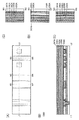
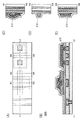
- 4A and 4B are a top view and a cross-sectional view of a semiconductor device according to one embodiment of the present invention.
- 6 is a flowchart illustrating a method for manufacturing a semiconductor device according to one embodiment of the present invention.
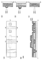
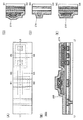
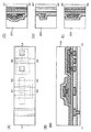
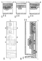
- 4A to 4D illustrate a method for manufacturing a transistor according to one embodiment of the present invention.
- 4A to 4D illustrate a method for manufacturing a transistor according to one embodiment of the present invention.
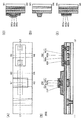
- 4A to 4D illustrate a method for manufacturing a transistor according to one embodiment of the present invention.
- 4A to 4D illustrate a method for manufacturing a transistor according to one embodiment of the present invention.
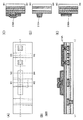
- 4A to 4D illustrate a method for manufacturing a transistor according to one embodiment of the present invention.
- 4A to 4D illustrate a method for manufacturing a transistor according to one embodiment of the present invention.
- 4A to 4D illustrate a method for manufacturing a transistor according to one embodiment of the present invention.
- 4A to 4D illustrate a method for manufacturing a transistor according to one embodiment of the present invention.
- 4A to 4D illustrate a method for manufacturing a transistor according to one embodiment of the present invention.
- 4A to 4D illustrate a method for manufacturing a transistor according to one embodiment of the present invention.
- 4A to 4D illustrate a method for manufacturing a transistor according to one embodiment of the present invention.
- 4A to 4D illustrate a method for manufacturing a transistor according to one embodiment of the present invention.
- FIG. 4A and 4B are a top view and a cross-sectional view of a semiconductor device according to one embodiment of the present invention.
- FIG. 6 is a cross-sectional view of a semiconductor device according to one embodiment of the present invention.
- FIG. 6 is a cross-sectional view of a semiconductor device according to one embodiment of the present invention.
- FIG. 6 is a cross-sectional view of a semiconductor device according to one embodiment of the present invention.
- FIG. 6 is a cross-sectional view of a semiconductor device according to one embodiment of the present invention.
- FIG. 6 is a top view illustrating a manufacturing apparatus according to one embodiment of the present invention.
- FIG. 6 is a top view illustrating a chamber according to one embodiment of the present invention.
- FIG. 6 is a top view illustrating a chamber according to one embodiment of the present invention.
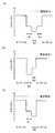
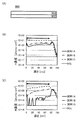
- the figure explaining the structure and SIMS result of a present Example The figure explaining the structure of a present Example.
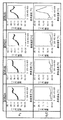
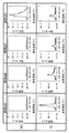
- the figure explaining the structure and TDS result of a present Example The figure explaining the structure and TDS result of a present Example.
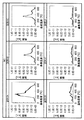
- the figure explaining the structure and SIMS result of a present Example The figure explaining the structure and SIMS result of a present Example.
- ordinal numbers such as “first” and “second” are used to avoid confusion between components, and do not indicate any order or order such as process order or stacking order.
- an ordinal number may be added in the claims to avoid confusion between the constituent elements.
- terms having an ordinal number in this specification and the like may have different ordinal numbers in the claims.
- terms with ordinal numbers are sometimes omitted in the claims.
- the terms “upper” and “lower” do not limit that the positional relationship between the components is directly above or directly below and is in direct contact.
- the expression “electrode B on the insulating layer A” does not require the electrode B to be formed in direct contact with the insulating layer A, and another configuration between the insulating layer A and the electrode B. Do not exclude things that contain elements.
- the channel length refers to, for example, a region where a semiconductor (or a portion where current flows in the semiconductor when the transistor is on) and a gate electrode overlap with each other in a top view of the transistor, or a region where a channel is formed
- the channel length is not necessarily the same in all regions. That is, the channel length of one transistor may not be fixed to one value. Therefore, in this specification, the channel length is any one of values, the maximum value, the minimum value, or the average value in a region where a channel is formed.
- the channel width is, for example, a region in which a semiconductor (or a portion in which a current flows in the semiconductor when the transistor is on) and a gate electrode overlap each other, or a source and a drain in a region where a channel is formed. This is the length of the part. Note that in one transistor, the channel width is not necessarily the same in all regions. That is, the channel width of one transistor may not be fixed to one value. Therefore, in this specification, the channel width is any one of values, the maximum value, the minimum value, or the average value in a region where a channel is formed.
- the impurity of the semiconductor means, for example, a component other than the main component constituting the semiconductor.
- an element having a concentration of less than 0.1 atomic% can be said to be an impurity.
- impurities for example, DOS (Density of States) of a semiconductor may increase, carrier mobility may decrease, or crystallinity may decrease.
- examples of the impurity that changes the characteristics of the semiconductor include a Group 1 element, a Group 2 element, a Group 13 element, a Group 14 element, a Group 15 element, and an oxide semiconductor.
- water may also function as an impurity.
- oxygen vacancies may be formed, for example, by mixing impurities.
- impurities that change the characteristics of the semiconductor include group 1 elements, group 2 elements, group 13 elements, and group 15 elements excluding oxygen and hydrogen.
- Embodiment 1 a semiconductor device provided with a transistor having favorable reliability and a manufacturing method of the semiconductor device will be described with reference to FIGS.
- an oxide semiconductor is used as an active layer. By reducing impurities such as water or hydrogen in the oxide semiconductor and supplying excess oxygen to reduce oxygen vacancies, the reliability of the transistor provided in the semiconductor device can be improved.
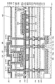
- the semiconductor device 1000 includes a transistor 200 and a transistor 400.
- Transistor 200 and transistor 400 formed over a substrate (not shown) have different structures.
- the transistor 400 may have a smaller drain current (hereinafter referred to as Icut) when the back gate voltage and the top gate voltage are 0 V than the transistor 200.
- Icut drain current
- the transistor 400 is used as a switching element so that the potential of the back gate of the transistor 200 can be controlled. Accordingly, after the node connected to the back gate of the transistor 200 is set to a desired potential, the transistor 400 is turned off, whereby the charge of the node connected to the back gate of the transistor 200 is prevented from being lost. it can.
- FIG. 1A is a top view of the semiconductor device 1000.
- FIG. 1B corresponds to the dashed-dotted line L1-L2 in FIG. 1A and is a cross-sectional view of the transistor 200 and the transistor 400 in the channel length direction.
- 1C corresponds to the one-dot chain line W1-W2 in FIG. 1A and is a cross-sectional view of the transistor 200 in the channel width direction.
- FIG. 1D is a cross-sectional view of the transistor 200 corresponding to the dashed-dotted line W3-W4 in FIG.
- FIG. 1E corresponds to the dashed-dotted line W5-W6 in FIG. 1A and is a cross-sectional view of the transistor 400 in the channel width direction.
- the transistor 200 includes an insulator 212 provided over the insulator 210, and an insulator 212.
- An insulator 214 disposed on the conductor, a conductor 205 (conductor 205a and conductor 205b) disposed on the insulator 214, an insulator 220 disposed on the conductor 205, and an insulator 222, insulator 224, oxide 230 disposed on insulator 224 (oxide 230a, oxide 230b, and oxide 230c), conductor 240a disposed on oxide 230b, and
- the conductor 240b (hereinafter, the conductor 240a and the conductor 240b are collectively referred to as the conductor 240), the layer 245a and the layer 245b (hereinafter, the layer 245a, and 245b collectively referred to as layer 245), an insulator 250 disposed over the oxide 230c, and
- the insulator 212 and the insulator 214 are preferably formed using an insulating material that does not easily transmit impurities such as water or hydrogen.
- an insulating material that does not easily transmit impurities such as water or hydrogen.
- aluminum oxide or the like is preferably used.
- impurities such as hydrogen and water from a lower layer than the insulator 210 can be prevented from diffusing into an upper layer than the insulator 212 and the insulator 214.
- the insulator 212 and the insulator 214 include a hydrogen atom, a hydrogen molecule, a water molecule, an oxygen atom, an oxygen molecule, a nitrogen atom, a nitrogen molecule, a nitrogen oxide molecule (N 2 O, NO, NO 2, and the like), a copper atom, and the like. It is preferable that at least one of the impurities is hardly transmitted. The same applies to the case where an insulating material which does not easily transmit impurities is described below.
- the insulator 212 is preferably formed using an atomic layer deposition (ALD) method.
- ALD atomic layer deposition
- the insulator 214 is preferably formed by a sputtering method. Accordingly, film formation can be performed at a higher film formation speed than that of the insulator 212, and the film thickness can be increased with higher productivity than the insulator 212. With such a stack of the insulator 212 and the insulator 214, barrier properties against impurities such as hydrogen and water can be improved.
- the insulator 212 may be provided below the insulator 214. In the case where the insulator 214 has a sufficient barrier property against impurities, the insulator 212 may not be provided.
- the insulator 212 and the insulator 214 are preferably formed using an insulating material which does not easily transmit oxygen. Thus, downward diffusion of oxygen contained in the insulator 224 and the like can be suppressed. Accordingly, oxygen can be effectively supplied to the oxide 230b.
- an opening is formed in the insulator 210, the insulator 212, and the insulator 214, and the insulator 210, the insulator 212, and the insulator 214 are on the same plane inside the opening.
- a plurality of openings are formed in the insulator 216, one of which is formed so as to overlap with the positions of the openings of the insulator 210, the insulator 212, and the insulator 214, and the diameter of the opening is the insulator 210 , Larger than the openings of the insulator 212 and the insulator 214. Further, the other opening of the insulator 216 reaches the upper surface of the insulator 214.
- a conductor 205a is formed in contact with the inside of the opening of the insulator 216, and a conductor 205b is formed further inside.
- the heights of the upper surfaces of the conductors 205a and 205b and the height of the upper surface of the insulator 216 can be approximately the same.
- the conductor 205a and the conductor 207a be formed using a conductive material that does not easily transmit impurities such as water or hydrogen.
- a conductive material that does not easily transmit impurities such as water or hydrogen.
- tantalum, tantalum nitride, ruthenium, ruthenium oxide, or the like is preferably used, which may be a single layer or a stacked layer. Accordingly, impurities such as hydrogen and water from the lower layer than the insulator 210 can be prevented from diffusing into the upper layer through the conductor 205 or the conductor 207.
- the concentration of impurities such as water, hydrogen, or nitrogen oxide in the insulator 224 is preferably reduced.
- the amount of hydrogen desorbed from the insulator 224 is 2 ⁇ 10 15 in terms of the amount of hydrogen desorbed in terms of hydrogen molecules in the range of 50 ° C. to 500 ° C. in TDS. Molecules / cm 2 or less, preferably 1 ⁇ 10 15 molecules / cm 2 or less, more preferably 5 ⁇ 10 14 molecules / cm 2 or less.
- the oxide 230b an oxide having an electron affinity higher than those of the oxide 230a and the oxide 230c is used.
- the oxide 230b has an electron affinity of 0.07 eV to 1.3 eV, preferably 0.1 eV to 0.7 eV, more preferably 0.1 eV to 0.4 eV, compared to the oxide 230a and the oxide 230c.
- the electron affinity is the difference between the vacuum level and the energy at the bottom of the conduction band.
- one of the conductor 205 and the conductor 260 can function as a gate electrode, and the other can function as a back gate electrode.
- the gate electrode and the back gate electrode are disposed so as to sandwich a semiconductor channel formation region.
- the potential of the back gate electrode may be the same as that of the gate electrode, or may be a ground potential or an arbitrary potential.
- the threshold voltage of the transistor can be changed by changing the potential of the back gate electrode independently of the gate electrode.
- the insulator 272 and the insulator 274 are preferably formed using an insulating material that does not easily transmit impurities such as water or hydrogen.
- an insulating material that does not easily transmit impurities such as water or hydrogen.
- aluminum oxide or the like is preferably used.
- the threshold voltage of the transistor 400 can be higher than that of the transistor 200 by using a semiconductor whose electron affinity is lower than that of the oxide 230b for the oxide 430.
- the oxide 430 and the oxide 230b are In-M-Zn oxide (an oxide containing In, the element M, and Zn)
- y 1 / x 1 is larger than y 2 / x 2
- the oxide 430 and the oxide 230b may be used.
- the hydrogen concentration in the insulator is 2 ⁇ 10 20 atoms / cm 3 or less, preferably 5 ⁇ 10 19 atoms / cm 3 or less, more preferably 1 ⁇ 10 19 atoms / cm 3 or less in SIMS, More preferably, it is 5 ⁇ 10 18 atoms / cm 3 or less.
- the hydrogen concentration of the insulator 216, the insulator 224, the insulator 250, the insulator 450, and the insulator 280 is preferably reduced. At least the hydrogen concentration of the insulator 224, the insulator 250, and the insulator 450 in contact with the oxide 230 or the oxide 430 is preferably reduced.
- a signal due to nitrogen dioxide (NO 2 ) may be observed.
- the signal is split into three signals by N nuclear spins, each having a g value of 2.037 or more and 2.039 or less (referred to as the first signal), and a g value of 2.001 or more and 2.003.
- the g value is observed below (referred to as the second signal) and from 1.964 to 1.966 (referred to as the third signal).
- a silicon oxynitride layer can be used as the insulating layer that emits less nitrogen oxide (NO x ).
- the silicon oxynitride layer is a film in which the amount of released ammonia is larger than the amount of released nitrogen oxide (NO x ) in TDS.
- the amount of released ammonia is 1 ⁇ 10 18 pieces / cm 3 or more 5 ⁇ 10 19 pieces / cm 3 or less.
- the amount of ammonia released is the total amount when the temperature of the heat treatment in TDS is 50 ° C. or higher and 650 ° C. or lower, or 50 ° C. or higher and 550 ° C. or lower.
- the insulating layer containing excess oxygen can also be formed by performing treatment for adding oxygen to the insulating layer.
- the treatment for adding oxygen can be performed by heat treatment under an oxygen atmosphere, ion implantation, ion doping, plasma immersion ion implantation, plasma treatment, or the like.
- the plasma treatment including oxygen it is preferable to use an apparatus having a power source that generates high-density plasma using, for example, microwaves.
- a power supply for applying RF (Radio Frequency) may be provided on the substrate side.
- RF Radio Frequency
- FIGS. 26A, 26B, and 26C a preferable range of the atomic ratio of indium, element M, and zinc included in the oxide according to the present invention will be described. Note that FIG. 26A, FIG. 26B, and FIG. 26C do not describe the atomic ratio of oxygen. In addition, each term of the atomic ratio of indium, element M, and zinc included in the oxide is [In], [M], and [Zn].
- a plurality of phases may coexist in the oxide (two-phase coexistence, three-phase coexistence, etc.).
- two phases of a spinel crystal structure and a layered crystal structure tend to coexist.
- two phases of a bixbite type crystal structure and a layered crystal structure tend to coexist.
- a crystal grain boundary may be formed between different crystal structures.
- the oxide can increase the carrier mobility (electron mobility) of the oxide by increasing the content of indium. That is, an oxide having a high indium content has higher carrier mobility than an oxide having a low indium content.
- CAAC-OS is an oxide with high crystallinity.
- CAAC-OS cannot confirm a clear crystal grain boundary, it can be said that a decrease in electron mobility due to the crystal grain boundary hardly occurs.
- the crystallinity of the oxide may be deteriorated by entry of impurities, generation of defects, or the like, the CAAC-OS can be said to be an oxide with few impurities and defects (such as oxygen vacancies). Therefore, the physical property of the oxide including the CAAC-OS is stable. Therefore, an oxide including a CAAC-OS is resistant to heat and has high reliability.
- an oxide with low carrier density is preferably used.
- the impurity concentration in the oxide semiconductor film may be decreased and the defect level density may be decreased.
- a low impurity concentration and a low density of defect states are referred to as high purity intrinsic or substantially high purity intrinsic.
- the oxide has a carrier density of less than 8 ⁇ 10 11 / cm 3 , preferably less than 1 ⁇ 10 11 / cm 3 , more preferably less than 1 ⁇ 10 10 / cm 3 , and 1 ⁇ 10 ⁇ 9 / cm 3. It may be 3 or more.
- an oxide that is highly purified intrinsic or substantially highly purified intrinsic has a low defect level density and thus may have a low trap level density.
- the charge trapped in the trap level of the oxide takes a long time to disappear, and may behave as if it were a fixed charge. Therefore, a transistor in which a channel region is formed in an oxide having a high trap state density may have unstable electrical characteristics.
- the concentration of silicon and carbon in the oxide and the concentration of silicon and carbon in the vicinity of the interface with the oxide are 2 ⁇ 10. 18 atoms / cm 3 or less, preferably 2 ⁇ 10 17 atoms / cm 3 or less.
- the oxide contains an alkali metal or an alkaline earth metal
- a defect level may be formed and carriers may be generated. Therefore, a transistor including an oxide containing an alkali metal or an alkaline earth metal is likely to be normally on. Therefore, it is preferable to reduce the concentration of alkali metal or alkaline earth metal in the oxide.
- the concentration of alkali metal or alkaline earth metal in the oxide obtained by SIMS is set to 1 ⁇ 10 18 atoms / cm 3 or less, preferably 2 ⁇ 10 16 atoms / cm 3 or less.
- the nitrogen concentration in the oxide is less than 5 ⁇ 10 19 atoms / cm 3 , preferably 5 ⁇ 10 18 atoms / cm 3 in SIMS. cm 3 or less, more preferably 1 ⁇ 10 18 atoms / cm 3 or less, and even more preferably 5 ⁇ 10 17 atoms / cm 3 or less.
- the oxide S1 and the oxide S3 have an energy level at the lower end of the conduction band closer to the vacuum level than the oxide S2.
- the energy level at the lower end of the conduction band of the oxide S2, and the oxide S1 The difference from the energy level at the lower end of the conduction band of the oxide S3 is preferably 0.15 eV or more, or 0.5 eV or more, and 2 eV or less, or 1 eV or less. That is, the difference between the electron affinity of the oxides S1 and S3 and the electron affinity of the oxide S2 is preferably 0.15 eV or more, or 0.5 eV or more, and 2 eV or less, or 1 eV or less.
- the energy level at the lower end of the conduction band changes gently. In other words, it can be said that it is continuously changed or continuously joined.
- the density of defect states in the mixed layer formed at the interface between the oxide S1 and the oxide S2 or the interface between the oxide S2 and the oxide S3 is preferably low.
- the oxide 230a and the oxide 230c may be gallium oxide.
- gallium oxide is used as the oxide 230c, leakage current generated between the conductor 205 and the oxide 230 can be reduced. That is, the off-state current of the transistor 200 can be reduced.
- the above conductive materials may be used for the layer 245a, the layer 245b, the layer 270, and the layer 470.
- a conductive material it is preferable to use a conductive material in which oxygen is hardly released and / or absorbed.
- step S07 the substrate temperature is set to 100 ° C. or higher and heat treatment is performed for about 5 minutes. Accordingly, moisture such as adsorbed water can be removed before the insulator 272 is formed. In particular, by performing heat treatment in an oxygen gas atmosphere, heat treatment can be performed without forming oxygen vacancies in the oxide 230. Subsequently, as illustrated in step S08, an insulator 272 is formed by a sputtering method. Here, as shown in the flowchart, the insulator 272 is continuously formed without being exposed to the outside air from the heat treatment in step S07.
- a high-quality film can be obtained at a relatively low temperature.
- a film formation method that does not use plasma at the time of film formation such as an MOCVD method, an ALD method, or a thermal CVD method, a film on which a surface is formed is hardly damaged and a film with few defects is obtained.
- the oxide 230A and part of the oxide 230B are selectively removed using the conductive film 240B as a mask (see FIGS. 10A to 10E). At this time, part of the insulator 224 may be removed at the same time. After that, the resist mask is removed to form a stacked structure of island-shaped oxide 230a, island-shaped oxide 230b, island-shaped conductive film 240B, layers 245a and 245b, and conductors 247a and 247b. can do.
- the conductors 247a and 247b function as hard masks, and the conductors 247a and 247b are also removed as the etching progresses.
- the conductor 240a and the conductor 240b function as a source electrode and a drain electrode of the transistor, the length of the distance between the conductor 240a and the conductor 240b facing each other is referred to as a channel length of the transistor. Can do. That is, when the opening of the film 245B is set to the minimum processing dimension, the distance between the layer 245a and the layer 245b is the minimum processing dimension, so that a gate line width and a channel length smaller than the minimum processing dimension can be formed. .
- part of the top surface of the conductive film 240B is covered with the layers 245a and 245b during the heat treatment, so that oxidation from the top surface can be prevented.
- an oxide film 230 ⁇ / b> C and an oxide film 230 ⁇ / b> C to be the oxide 430 later are formed.
- the oxide film 230C is formed using an oxide containing a large amount of excess oxygen similarly to the oxide film 230A.
- oxygen can be supplied to the oxide 230b by a subsequent heat treatment.
- one or both of oxygen doping treatment and heat treatment may be performed.
- oxygen contained in the oxide 230a and the oxide 230c can be supplied to the oxide 230b.
- oxygen vacancies in the oxide 230b can be reduced. Therefore, when an oxygen-deficient oxide is used for the oxide 230b, a semiconductor containing excess oxygen is preferably used for the oxide 230c.
- the conductive film 260A, the conductive film 260B, and the conductive film 260C are formed in this order (see FIGS. 14A to 14E).
- a metal oxide formed by a sputtering method is used as the conductive film 260A
- titanium nitride is used as the conductive film 260B
- tungsten is used as the conductive film 260C.
- oxygen can be added to the insulator 250 so that the oxygen is in an excess state. Accordingly, oxygen can be effectively supplied from the insulator 250 to the oxide 230b.
- part of the film 270A is selectively removed using a photolithography method, so that the layer 270 and the layer 470 functioning as a gate cap are formed.
- the layer 270 and the layer 470 functioning as a gate cap are formed.
- the oxide film 230C is etched using the layer 270 and the layer 470 as a mask (see FIGS. 17A to 17E).
- the etching treatment in this step may be performed by wet etching or the like.
- wet etching is performed using phosphoric acid.
- the island-shaped oxide 230c and the island-shaped oxide 430 are formed. Even when a part of the oxide film 230C remains as a residue, the oxide film 230C can be removed to expose the side surface of the oxide 230b.
- the temperature is preferably 410 ° C. or lower, more preferably 400 ° C. or lower.
- the heating temperature is preferably higher than the substrate temperature at the time of film formation of the insulator 272 described later.
- the insulator 272 and the insulator 274 have a function of releasing hydrogen contained in the insulator 224, the oxide 230a, the oxide 230b, and the like as water to the outside of the insulator 274. Note that when the insulator 272 is formed at a low temperature, the function of gettering impurities in the film such as the oxide 230b is improved.
- the substrate is carried into a film formation apparatus having a plurality of chambers, and heat treatment is performed in the chamber of the film formation apparatus.
- impurities such as moisture adsorbed on the substrate before the insulator 282 can be formed can be removed.
- the insulator 282 is formed by a sputtering method in a chamber different from the chamber in which the heat treatment of the film formation apparatus is performed. The insulator 282 is formed continuously without being exposed to the outside air from the immediately preceding heat treatment.
- the insulator 284 is formed over the insulator 282 by an ALD method (see FIGS. 22A to 22E).
- the semiconductor device described in this embodiment is not limited to that illustrated in FIG. For example, it is good also as a structure as shown in FIG.
- the semiconductor device 1000 illustrated in FIG. 23 includes a region in which the layer 270, the insulator 250, and the oxide 230c extend beyond the end portion of the conductor 260 and overlap and overlap with each other in the extending portion. 1 is different from the semiconductor device 1000 shown in FIG. 1 in that the end portion of 270, the end portion of the insulator 250, and the end portion of the oxide 230c are substantially coincident.
- the insulator 272 and the side surface of the insulator 250 are in contact with each other. Accordingly, oxygen can be added from the insulator 272 to the insulator 250. Further, impurities such as hydrogen contained in the insulator 250 can be gettered to the insulator 272 and diffused outward.
- one embodiment of the present invention can provide a semiconductor device with favorable reliability.
- a semiconductor device including an oxide with reduced impurities can be provided.
- a semiconductor device including an oxide with reduced oxygen vacancies can be provided.
- the back gate voltage of the transistor 200 is controlled by the transistor 400.
- the top gate and the back gate of the transistor 400 are diode-connected to the source, and the source of the transistor 400 and the back gate of the transistor 200 are connected.
- the negative potential of the back gate of the transistor 200 is held in this configuration, the voltage between the top gate and the source of the transistor 400 and the voltage between the back gate and the source are 0V.
- the Icut of the transistor 400 is very small. Therefore, with this structure, the negative potential of the back gate of the transistor 200 can be maintained for a long time without supplying power to the transistor 200 and the transistor 400.
- the memory device including the transistor 200 and the transistor 400 can hold stored data for a long time.
- the memory device illustrated in FIGS. 28 and 29 has a characteristic that the potential of the gate of the transistor 300 can be held, so that information can be written, held, and read as described below.
- a memory cell array can be formed by arranging the memory devices shown in FIGS. 28 and 29 in a matrix.
- a desired potential can be obtained by supplying the wiring 3005 with a potential at which the transistor 300 becomes “non-conductive” regardless of the charge applied to the node FG, that is, a potential lower than V th_H. Only the memory cell information can be read out.
- the transistor 300 is an n-channel transistor, the memory cell has a NAND structure.
- the memory device illustrated in FIGS. 28 and 29 may not include the transistor 300. Even when the transistor 300 is not provided, information writing and holding operations can be performed by operations similar to those of the memory device described above.
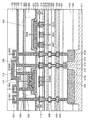
- FIG. 1 An example of a memory device of one embodiment of the present invention is illustrated in FIG.
- the memory device includes a transistor 400, a transistor 300, a transistor 200, and a capacitor 100.
- the transistor 200 is provided above the transistor 300
- the capacitor 100 is provided above the transistor 300 and the transistor 200.
- the transistor 300 includes a conductor 316, an insulator 314, a semiconductor region 312 formed of part of the substrate 311, a low resistance region 318a functioning as a source region or a drain region, and a low resistance region 318b. Have.
- the region in which the channel of the semiconductor region 312 is formed, the region in the vicinity thereof, the low resistance region 318a serving as the source region or the drain region, the low resistance region 318b, and the like preferably include a semiconductor such as a silicon-based semiconductor. It preferably contains crystalline silicon. Alternatively, a material containing Ge (germanium), SiGe (silicon germanium), GaAs (gallium arsenide), GaAlAs (gallium aluminum arsenide), or the like may be used. A structure using silicon in which effective mass is controlled by applying stress to the crystal lattice and changing the lattice spacing may be employed. Alternatively, the transistor 300 may be a HEMT (High Electron Mobility Transistor) by using GaAs, GaAlAs, or the like.
- HEMT High Electron Mobility Transistor
- an insulator having a barrier property against hydrogen is preferably used as in the case of the insulator 324.
- the conductor 356 preferably includes a conductor having a barrier property against hydrogen.
- a conductor having a barrier property against hydrogen is formed in an opening portion of the insulator 350 having a barrier property against hydrogen.
- a conductor 285 and the like are embedded in the insulator 220, the insulator 222, the insulator 224, the insulator 272, the insulator 274, and the insulator 110.
- the conductor 287 functions as a plug or a wiring electrically connected to the capacitor 100, the transistor 200, or the transistor 300.
- the conductor 112 functions as one of the electrodes of the capacitor 100. Note that the conductor 287 and the conductor 112 can be formed at the same time.
- the conductor 287 and the conductor 112 include a metal film containing an element selected from molybdenum, titanium, tantalum, tungsten, aluminum, copper, chromium, neodymium, and scandium, or a metal nitride film containing any of the above elements as a component (Tantalum nitride, titanium nitride film, molybdenum nitride film, tungsten nitride film) or the like can be used.
- the insulator 130, the insulator 132, and the insulator 134 include, for example, silicon oxide, silicon oxynitride, silicon nitride oxide, silicon nitride, aluminum oxide, aluminum oxynitride, aluminum nitride oxide, aluminum nitride, hafnium oxide, hafnium oxynitride, Nitride hafnium oxide, hafnium nitride, or the like may be used, and a stacked layer or a single layer can be used.
- An insulator 150 is provided over the conductor 116 and the insulator 134.
- the insulator 150 can be provided using a material similar to that of the insulator 320. Further, the insulator 150 may function as a planarization film that covers the concave and convex shapes below the insulator 150.
- the partial pressure of the gas molecule (atom) whose m / z is 28 in the transfer chamber 2704 and each chamber is, for example, 3 ⁇ 10 ⁇ 5 Pa or less, preferably 1 ⁇ 10 ⁇ 5 Pa or less, more preferably 3 ⁇ 10 ⁇ 6 Pa or less.
- the partial pressure of the gas molecule (atom) whose m / z is 44 in the transfer chamber 2704 and each chamber is, for example, 3 ⁇ 10 ⁇ 5 Pa or less, preferably 1 ⁇ 10 ⁇ 5 Pa or less, and more preferably 3 ⁇ 10 ⁇ 6 Pa or less.
- the total pressure and partial pressure in the transfer chamber 2704 and each chamber can be measured using a mass spectrometer.
- a mass spectrometer also referred to as Q-mass
- Q-mass Qulee CGM-051 manufactured by ULVAC, Inc.
- the transfer chamber 2704 and each chamber have a small external leak or internal leak.
- the leak rate of the transfer chamber 2704 and each chamber is 3 ⁇ 10 ⁇ 6 Pa ⁇ m 3 / s or less, preferably 1 ⁇ 10 ⁇ 6 Pa ⁇ m 3 / s or less.
- the leak rate of a gas molecule (atom) having an m / z of 18 is 1 ⁇ 10 ⁇ 7 Pa ⁇ m 3 / s or less, preferably 3 ⁇ 10 ⁇ 8 Pa ⁇ m 3 / s or less.
- a member constituting the manufacturing apparatus 2700 aluminum, chromium, titanium, zirconium, nickel, or vanadium that emits less impurities and contains less impurities is used. Further, the above-described member may be used by being coated with an alloy containing iron, chromium, nickel and the like. Alloys containing iron, chromium, nickel, etc. are rigid, heat resistant and suitable for processing. Here, if the surface irregularities of the member are reduced by polishing or the like in order to reduce the surface area, the emitted gas can be reduced.
- the adsorbate present in the transfer chamber 2704 and each chamber does not affect the pressure in the transfer chamber 2704 and each chamber because it is adsorbed on the inner wall and the like, but causes of gas release when the transfer chamber 2704 and each chamber are exhausted It becomes. Therefore, although there is no correlation between the leak rate and the exhaust speed, it is important to desorb as much as possible the adsorbate present in the transfer chamber 2704 and each chamber using a pump having a high exhaust capability and exhaust it in advance.
- the transfer chamber 2704 and each chamber may be baked to promote desorption of the adsorbate. Baking can increase the desorption rate of the adsorbate by about 10 times. Baking may be performed at 100 ° C to 450 ° C.
- the desorption rate of water or the like that is difficult to desorb only by exhausting can be further increased.
- the desorption rate of the adsorbate can be further increased.
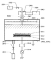
- the high-frequency generator 2803 has a function of generating a microwave of 0.3 GHz to 3.0 GHz, 0.7 GHz to 1.1 GHz, or 2.2 GHz to 2.8 GHz, for example.
- the microwave generated by the high frequency generator 2803 is transmitted to the mode converter 2805 through the waveguide 2804.
- the microwave transmitted as the TE mode is converted into the TEM mode.
- the microwave is transmitted to the slot antenna plate 2808 through the waveguide 2807.
- the slot antenna plate 2808 is provided with a plurality of slot holes, and the microwave passes through the slot holes and the dielectric plate 2809. Then, an electric field can be generated below the dielectric plate 2809 to generate high-density plasma 2810.
- ions and radicals corresponding to the gas species supplied from the gas supply source 2801 exist. For example, oxygen radicals or nitrogen radicals exist.
- Samples 1A to 1C each include a substrate 902 and an insulator 904 over the substrate 902 as a structure 900 illustrated in FIG.
- Sample 1A a sample in which microwave excitation plasma treatment was performed on the insulator 904 while applying an RF bias to the substrate was referred to as Sample 1A.
- Sample 1B A sample in which the insulator 904 was subjected to microwave excitation plasma treatment without an RF bias was referred to as Sample 1B.
- Sample 1C a sample in which the insulator 904 was not subjected to the microwave excitation plasma treatment was designated as Sample 1C.
- the sample 2A to the sample 2C were subjected to microwave excitation plasma treatment for 60 minutes using a microwave plasma treatment apparatus.
- the microwave-excited plasma treatment was performed in an atmosphere of argon (Ar) with a flow rate of 150 sccm and oxygen (O 2 ) with a flow rate of 50 sccm.
- the pressure of the reaction chamber was 60 Pa, a high frequency (RF) bias of 13.56 MHz was applied, and plasma was generated by a microwave of 4000 W (2.45 GHz).
- microwave-excited plasma processing step for sample 2A plasma processing was performed while applying a high frequency (RF) bias of 600 W.
- microwave-excited plasma processing step for sample 2B plasma processing was performed while applying a 300 W radio frequency (RF) bias.
- RF radio frequency
- Samples 4A to 4H include a substrate 922, an insulator 924 over the substrate 922, an oxide 926 over the insulator 924, and an insulator 928 over the oxide 926 as a structure 920 illustrated in FIG. And an insulator 930 over the insulator 928.
- a silicon substrate was prepared as the substrate 922.
- a thermal oxide film having a thickness of 100 nm was formed as an insulator 924 over the substrate 922.
- SIMS measurement results of each sample> SIMS analysis was performed from the substrate side using the oxide 926 of Samples 4A to 4H as a quantitative layer, and the results of detecting the hydrogen (H) concentration are shown in FIGS. 42 (B) to 42 (E).
- the hydrogen concentration was evaluated by secondary ion mass spectrometry (SIMS), and a dynamic SIMS device IMS-7f manufactured by CAMECA was used as an analyzer.
- SIMS secondary ion mass spectrometry
- FIG. 42D and FIG. 42B indicate that hydrogen in the oxide 926 can be reduced by performing heat treatment after the insulator 930 is formed. 42D and 42C, the oxide 926 is subjected to heat treatment after the insulator 930 is formed even when the temperature of the insulator 928 is high. It has been found that the hydrogen in it can be reduced to the background level.
- hydrogen in the oxide can be reduced by performing heat treatment after contacting the oxide with aluminum oxide having a low deposition temperature.
- heat treatment is performed after stacking aluminum oxide deposited using a sputtering method and aluminum oxide deposited using an ALD method on an oxide, thereby effectively reducing hydrogen in the oxide. I understood that I could do it.
Landscapes
- Physics & Mathematics (AREA)
- Engineering & Computer Science (AREA)
- Plasma & Fusion (AREA)
- Chemical & Material Sciences (AREA)
- Analytical Chemistry (AREA)
- Thin Film Transistor (AREA)
- Semiconductor Memories (AREA)
- Metal-Oxide And Bipolar Metal-Oxide Semiconductor Integrated Circuits (AREA)
- Non-Volatile Memory (AREA)
- Optics & Photonics (AREA)
Abstract
Description
本実施の形態では、良好な信頼性を有するトランジスタが設けられた半導体装置、及び当該半導体装置の作製方法について、図1乃至図25を用いて説明する。本実施の形態に示す半導体装置に設けられたトランジスタでは、活性層として酸化物半導体を用いている。当該酸化物半導体中の水または水素などの不純物を低減させ、過剰酸素を供給して酸素欠損を低減させることにより、半導体装置に設けられたトランジスタの信頼性を向上させることができる。
図1(A)、図1(B)、図1(C)、図1(D)、および図1(E)は、半導体装置1000を示す上面図および断面図である。半導体装置1000はトランジスタ200およびトランジスタ400を有する。基板(図示せず)の上に形成されたトランジスタ200およびトランジスタ400は、異なる構成を有する。例えば、トランジスタ400は、トランジスタ200と比較して、バックゲート電圧及びトップゲート電圧が0Vのときのドレイン電流(以下、Icutと呼ぶ。)が小さい構成とすればよい。トランジスタ400をスイッチング素子として、トランジスタ200のバックゲートの電位を制御できる構成とする。これにより、トランジスタ200のバックゲートと接続するノードを所望の電位にした後、トランジスタ400をオフ状態にすることで、トランジスタ200のバックゲートと接続するノードの電荷が消失することを抑制することができる。
図1(A)、図1(B)、図1(C)、および図1(D)に示すように、トランジスタ200は、絶縁体210の上に配置された絶縁体212と、絶縁体212の上に配置された絶縁体214と、絶縁体214の上に配置された導電体205(導電体205a、および導電体205b)と、導電体205の上に配置された絶縁体220、絶縁体222、および絶縁体224と、絶縁体224の上に配置された酸化物230(酸化物230a、酸化物230b、および酸化物230c)と、酸化物230bの上に配置された導電体240a、および導電体240b(以下、導電体240a、および導電体240bをまとめて導電体240ともいう)と、導電体240の上に配置された層245a、および層245b(以下、層245a、および層245bをまとめて層245ともいう)と、酸化物230cの上に配置された絶縁体250と、絶縁体250の上に配置された導電体260(導電体260a、導電体260b、および導電体260c)と、導電体260cの上に配置された層270と、層270の上に配置された絶縁体272と、絶縁体272の上に配置された絶縁体274と、を有する。
図1(A)、図1(B)、図1(E)に示すように、トランジスタ400は、絶縁体210の上に配置された絶縁体212と、絶縁体212の上に配置された絶縁体214と、絶縁体214の上に配置された導電体403(導電体403a、および導電体403b)、導電体405(導電体405a、および導電体405b)、導電体407(導電体407a、および導電体407b)と、導電体403、導電体405、および導電体407の上に配置された絶縁体220、絶縁体222、および絶縁体224と、絶縁体224、導電体405、および導電体407の上に配置された酸化物430と、酸化物430の上に配置された絶縁体450と、絶縁体450の上に配置された導電体460(導電体460a、導電体460b、および導電体460c)と、導電体460cの上に配置された層470と、層470の上に配置された絶縁体272と、絶縁体272の上に配置された絶縁体274と、を有する。以下、トランジスタ200で説明した構成については省略する。
〔絶縁体〕
絶縁体210、絶縁体216、絶縁体220、絶縁体224、絶縁体250、絶縁体450、および絶縁体280は、例えば、ホウ素、炭素、窒素、酸素、フッ素、マグネシウム、アルミニウム、シリコン、リン、アルゴン、ガリウム、ゲルマニウム、イットリウム、ジルコニウム、ランタン、ネオジム、ハフニウムまたはタンタルを含む絶縁材料を、単層で、または積層で用いればよい。例えば、酸化シリコン、酸化窒化シリコン、窒化酸化シリコン、窒化シリコン、窒化アルミニウム、酸化アルミニウム、窒化酸化アルミニウム、酸化窒化アルミニウム、酸化マグネシウム、酸化ガリウム、酸化ゲルマニウム、酸化イットリウム、酸化ジルコニウム、酸化ランタン、酸化ネオジム、酸化ハフニウム、酸化タンタル、アルミニウムシリケートなどから選ばれた材料を、単層でまたは積層して用いる。また、酸化物材料、窒化物材料、酸化窒化物材料、窒化酸化物材料のうち、複数の材料を混合した材料を用いてもよい。
以下に、本発明に係る酸化物230、および酸化物430について説明する。
酸化物は、単結晶酸化物と、それ以外の非単結晶酸化物と、に分けられる。非単結晶酸化物としては、例えば、CAAC−OS(c−axis aligned crystalline oxide semiconductor)、多結晶酸化物、nc−OS(nanocrystalline oxide semiconductor)、擬似非晶質酸化物(a−like OS:amorphous−like oxide semiconductor)および非晶質酸化物などがある。
次に、図26(A)、図26(B)、および図26(C)を用いて、本発明に係る酸化物が有するインジウム、元素M及び亜鉛の原子数比の好ましい範囲について説明する。なお、図26(A)、図26(B)、および図26(C)には、酸素の原子数比については記載しない。また、酸化物が有するインジウム、元素M、及び亜鉛の原子数比のそれぞれの項を[In]、[M]、および[Zn]とする。
続いて、上記酸化物をトランジスタに用いる場合について説明する。
ここで、酸化物中における各不純物の影響について説明する。
続いて、該酸化物を2層構造、または3層構造とした場合について述べる。酸化物S1、酸化物S2、および酸化物S3の積層構造、および積層構造に接する絶縁体のバンド図と、酸化物S2および酸化物S3の積層構造、および積層構造に接する絶縁体のバンド図と、酸化物S1および酸化物S2の積層構造、および積層構造に接する絶縁体のバンド図と、について、図27を用いて説明する。
導電体205、導電体207、導電体403、導電体405、導電体407、導電体240、導電体260および導電体460を形成するための導電性材料としては、アルミニウム、クロム、銅、銀、金、白金、タンタル、ニッケル、チタン、モリブデン、タングステン、ハフニウム、バナジウム、ニオブ、マンガン、マグネシウム、ジルコニウム、ベリリウム、インジウムなどから選ばれた金属元素を1種以上含む材料を用いることができる。また、リン等の不純物元素を含有させた多結晶シリコンに代表される、電気伝導度が高い半導体、ニッケルシリサイドなどのシリサイドを用いてもよい。
基板として用いる材料に大きな制限はないが、少なくとも後の加熱処理に耐えうる程度の耐熱性を有していることが必要となる。例えば、基板としてシリコンや炭化シリコンなどを材料とした単結晶半導体基板、多結晶半導体基板、シリコンゲルマニウムなどを材料とした化合物半導体基板等を用いることができる。また、SOI基板や、半導体基板上に歪トランジスタやFIN型トランジスタなどの半導体素子が設けられたものなどを用いることもできる。または、高電子移動度トランジスタ(HEMT:High Electron Mobility Transistor)に適用可能なヒ化ガリウム、ヒ化アルミニウムガリウム、ヒ化インジウムガリウム、窒化ガリウム、リン化インジウム、シリコンゲルマニウムなどを用いてもよい。すなわち、基板は、単なる支持基板に限らず、他のトランジスタなどのデバイスが形成された基板であってもよい。この場合、トランジスタ200、またはトランジスタ400のゲート、ソース、またはドレインの少なくとも一つは、上記他のデバイスと電気的に接続されていてもよい。
半導体装置1000の作製方法例について図2乃至図25を用いて説明する。ここで、図2は半導体装置1000の作製工程の一部を示すフローチャートである。図2に示すフローチャートでは、左側に工程(ステップ)を記載し、右側に各工程に係る、水素または水などの不純物、及び酸素の挙動に関わる効果を示している。図24はマイクロ波によって励起されるプラズマ中に含まれるラジカル、およびイオンのエネルギー準位を説明する図である。また、図25は、酸化アルミニウムによる、酸化物中の水素を低減するメカニズムを説明する模式図である。
本実施の形態に示す半導体装置は図1に示すものに限られるものではない。例えば、図23に示すような構成としてもよい。
本実施の形態では、半導体装置の一形態を、図28乃至図30を用いて説明する。
本発明の一態様である半導体装置を使用した、記憶装置の一例を図28乃至図30に示す。
図28、および図29に示す記憶装置は、トランジスタ300のゲートの電位が保持可能という特性を有することで、以下に示すように、情報の書き込み、保持、読み出しが可能である。
図28、および図29に示す記憶装置は、トランジスタ300を有さない構成としてもよい。トランジスタ300を有さない場合も、先に述べた記憶装置と同様の動作により情報の書き込みおよび保持動作が可能である。
本発明の一態様の記憶装置の一例を、図28に示す。記憶装置は、トランジスタ400、トランジスタ300、トランジスタ200、容量素子100を有する。トランジスタ200はトランジスタ300の上方に設けられ、容量素子100はトランジスタ300、およびトランジスタ200の上方に設けられている。
記憶装置の変形例の一例を、図29に示す。図29は、図29と、トランジスタ300の構成、および絶縁体272、および絶縁体274の形状などが異なる。
また、本実施の形態の変形例の一例を、図30に示す。図30は、図30に示す記憶装置を、マトリクス状に配置した場合における、行の一部を抜き出した断面図である。
<製造装置>
以下では、本発明の一態様に係る高密度プラズマ処理を行う製造装置について説明する。
以下では、本発明の一態様に係る試料1A、試料1B、および試料1Cについて説明する。試料1A乃至試料1Cは、図34(A)に示す、構造900として、基板902と、基板902上の絶縁体904と、を有する。
次に、試料1A乃至試料1CにSIMS分析を行って水素(H)濃度、および窒素(N)濃度を検出した結果を図34(B)、および図34(C)に示す。なお、水素濃度評価は、二次イオン質量分析(Secondary Ion Mass Spectrometry:SIMS)により行い、分析装置としてアルバック・ファイ社製ダイナミックSIMS装置PHI ADEPT−1010を用いた。
以下では、本発明の一態様に係る試料2A、試料2B、試料2C、および試料2Dについて説明する。試料2A乃至試料2Dは、図35に示す、構造910として、基板912と、基板912上の絶縁体914と、絶縁体914上の絶縁体916を有する。
TDS分析を行った結果を、図36、および図37に示す。なお、当該TDS分析においては、水素分子に相当する質量電荷比m/z=2の放出量と、水分子に相当する質量電荷比m/z=18の放出量と、一酸化窒素に相当する質量電荷比m/z=30の放出量と、酸素分子に相当する質量電荷比m/z=32の放出量と、を測定した。TDS分析装置として、電子科学社製WA1000Sを使い、昇温レートは30℃/minとした。
以下では、本発明の一態様に係る試料3A、試料3B、試料3C、試料3D、試料3E、および試料2Fについて説明する。試料3A乃至試料3Fは、図35に示す、構造910として、基板912と、基板912上の絶縁体914と、絶縁体914上の絶縁体916を有する。
TDS分析を行った結果を、図38乃至図41に示す。なお、当該TDS分析においては、水素分子に相当する質量電荷比m/z=2の放出量と、水分子に相当する質量電荷比m/z=18の放出量と、一酸化窒素に相当する質量電荷比m/z=30の放出量と、酸素分子に相当する質量電荷比m/z=32の放出量と、を測定した。TDS分析装置として、電子科学社製WA1000Sを使い、昇温レートは30℃/minとした。
以下では、本発明の一態様に係る試料4A、試料4B、試料4C、試料4D、試料4E、試料4F、試料4G、および試料4Hについて説明する。試料4A乃至試料4Hは、図42(A)に示す、構造920として、基板922と、基板922上の絶縁体924と、絶縁体924上の酸化物926と、酸化物926上の絶縁体928と、絶縁体928上の絶縁体930と、を有する。

次に、試料4A乃至試料4Hの酸化物926を定量層として、基板側からSIMS分析を行い、水素(H)濃度を検出した結果を図42(B)、乃至図42(E)に示す。なお、水素濃度評価は、二次イオン質量分析(Secondary Ion Mass Spectrometry:SIMS)により行い、分析装置としてCAMECA社製ダイナミックSIMS装置IMS−7fを用いた。
101 容量素子
110 絶縁体
112 導電体
116 導電体
130 絶縁体
132 絶縁体
134 絶縁体
150 絶縁体
200 トランジスタ
201 トランジスタ
205 導電体
205a 導電体
205b 導電体
207 導電体
207a 導電体
207b 導電体
s210 絶縁体
212 絶縁体
214 絶縁体
216 絶縁体
218 導電体
220 絶縁体
222 絶縁体
224 絶縁体
226 絶縁体
230 酸化物
230a 酸化物
230A 酸化膜
230b 酸化物
230B 酸化膜
230c 酸化物
230C 酸化膜
240 導電体
240a 導電体
240A 導電膜
240b 導電体
240B 導電膜
245 層
245a 層
245A 膜
245b 層
245B 膜
247a 導電体
247A 導電膜
247b 導電体
247B 導電膜
250 絶縁体
250A 絶縁膜
260 導電体
260a 導電体
260A 導電膜
260b 導電体
260B 導電膜
260c 導電体
260C 導電膜
270 層
272 絶縁体
274 絶縁体
280 絶縁体
281 バルブ
282 絶縁体
284 絶縁体
285 導電体
287 導電体
290 レジストマスク
299 領域
300 トランジスタ
301 トランジスタ
311 基板
312 半導体領域
314 絶縁体
316 導電体
318a 低抵抗領域
318b 低抵抗領域
320 絶縁体
322 絶縁体
324 絶縁体
326 絶縁体
328 導電体
330 導電体
350 絶縁体
352 絶縁体
354 絶縁体
356 導電体
358 絶縁体
400 トランジスタ
403 導電体
403a 導電体
403b 導電体
405 導電体
405a 導電体
405b 導電体
405c 導電体
407 導電体
407a 導電体
407b 導電体
407c 導電体
430 酸化物
450 絶縁体
460 導電体
460a 導電体
460b 導電体
460c 導電体
470 層
480 開口
900 構造
902 基板
904 絶縁体
910 構造
912 基板
914 絶縁体
916 絶縁体
920 構造
922 基板
924 絶縁体
926 酸化物
928 絶縁体
930 絶縁体
1000 半導体装置
2700 製造装置
2701 大気側基板供給室
2702 大気側基板搬送室
2703a ロードロック室
2703b アンロードロック室
2704 搬送室
2706a チャンバー
2706b チャンバー
2706c チャンバー
2706d チャンバー
2761 カセットポート
2762 アライメントポート
2763a 搬送ロボット
2763b 搬送ロボット
2801 ガス供給源
2802 バルブ
2803 高周波発生器
2804 導波管
2805 モード変換器
2806 ガス管
2807 導波管
2808 スロットアンテナ板
2809 誘電体板
2810 高密度プラズマ
2811 基板
2812 基板ホルダ
2813 加熱機構
2815 マッチングボックス
2816 高周波電源
2817 真空ポンプ
2818 バルブ
2819 排気口
2820 ランプ
2821 ガス供給源
2822 バルブ
2823 ガス導入口
2824 基板
2825 基板ホルダ
2826 加熱機構
2827 真空ポンプ
2828 真空ポンプ
2829 バルブ
2830 排気口
3001 配線
3002 配線
3003 配線
3004 配線
3005 配線
3006 配線
3007 配線
3008 配線
3009 配線
3010 配線
Claims (7)
- 第1の導電体を形成し、
前記第1の導電体上に第1の絶縁体を形成し、
前記第1の絶縁体上に第2の絶縁体を形成し、
前記第2の絶縁体上に第3の絶縁体を形成し、
前記第3の絶縁体にマイクロ波励起プラズマ処理を行い、
前記第3の絶縁体上に、島状の第1の酸化物半導体と、前記第1の酸化物半導体上の第2の導電体、および第3の導電体と、を形成し、
前記第1の酸化物半導体、前記第2の導電体、および前記第3の導電体上に、酸化物半導体膜を形成し、
前記酸化物半導体膜上に、第1の絶縁膜を形成し、
前記第1の絶縁膜上に導電膜を形成し、
前記第1の絶縁膜、および前記導電膜の一部を除去し、第4の絶縁体、および第4の導電体を形成し、
前記酸化物半導体膜と、前記第4の絶縁体と、前記第4の導電体と、を覆うように、第2の絶縁膜を形成し、
前記酸化物半導体膜、および前記第2の絶縁膜、の一部を除去し、第2の酸化物半導体、および第5の絶縁体を形成することで、前記第1の酸化物半導体の側面を露出し、
前記第1の酸化物半導体の側面、および前記第2の酸化物半導体の側面と接して、第6の絶縁体を形成し、
前記第6の絶縁体と接して、第7の絶縁体を形成し、
加熱処理を行うことを特徴とする半導体装置の作製方法。 - 第1の導電体を形成し、
前記第1の導電体上に第1の絶縁体を形成し、
前記第1の絶縁体上に第2の絶縁体を形成し、
前記第2の絶縁体上に第3の絶縁体を形成し、
前記第3の絶縁体にマイクロ波励起プラズマ処理を行い、
前記第3の絶縁体上に、島状の第1の酸化物半導体と、前記第1の酸化物半導体上の第2の導電体、および第3の導電体と、を形成し、
前記第1の酸化物半導体、前記第2の導電体、および前記第3の導電体上に、酸化物半導体膜を形成し、
前記酸化物半導体膜上に、第1の絶縁膜を形成し、
前記第1の絶縁膜上に導電膜を形成し、
前記導電膜の一部を除去し、第4の導電体を形成し、
前記第1の絶縁膜と、前記第4の導電体と、を覆うように、第2の絶縁膜を形成し、
前記酸化物半導体膜、前記第1の絶縁膜、および前記第2の絶縁膜、の一部を除去し、第2の酸化物半導体、前記第4の絶縁体、および第5の絶縁体を形成することで、前記第1の酸化物半導体の側面を露出し、
前記第1の酸化物半導体の側面、および前記第2の酸化物半導体の側面と接して、第6の絶縁体を形成し、
前記第6の絶縁体と接して、第7の絶縁体を形成し、
加熱処理を行うことを特徴とする半導体装置の作製方法。 - 請求項1または請求項2において、
前記マイクロ波励起プラズマ処理は、圧力が70Pa以下で行うことを特徴とする半導体装置の作製方法。 - 請求項1または請求項2において、
前記マイクロ波励起プラズマ処理は、酸素流量比が10%以上30%以下で行うことを特徴とする半導体装置の作製方法。 - 請求項1または請求項2において、
前記マイクロ波励起プラズマ処理は、RFバイアスを基板に印加しながら、行うことを特徴とする半導体装置の作製方法。 - 請求項1または請求項2において、
前記第6の絶縁体は、120℃以上150℃以下の基板温度で、スパッタリング法により形成することを特徴とする半導体装置の作製方法。 - 請求項1または請求項2において、
前記第6の絶縁体は、成膜装置で100℃以上の加熱処理を行った後、前記成膜装置にて大気開放することなく、成膜することを特徴とする半導体装置の作製方法。
Priority Applications (3)
| Application Number | Priority Date | Filing Date | Title |
|---|---|---|---|
| US16/093,268 US20190139783A1 (en) | 2016-04-22 | 2017-04-11 | Semiconductor device and method for fabricating semiconductor device |
| JP2018512507A JP6902024B2 (ja) | 2016-04-22 | 2017-04-11 | 半導体装置の作製方法 |
| KR1020187030408A KR20180134919A (ko) | 2016-04-22 | 2017-04-11 | 반도체 장치 및 반도체 장치의 제작 방법 |
Applications Claiming Priority (2)
| Application Number | Priority Date | Filing Date | Title |
|---|---|---|---|
| JP2016-086299 | 2016-04-22 | ||
| JP2016086299 | 2016-04-22 |
Publications (1)
| Publication Number | Publication Date |
|---|---|
| WO2017182910A1 true WO2017182910A1 (ja) | 2017-10-26 |
Family
ID=60115798
Family Applications (1)
| Application Number | Title | Priority Date | Filing Date |
|---|---|---|---|
| PCT/IB2017/052071 Ceased WO2017182910A1 (ja) | 2016-04-22 | 2017-04-11 | 半導体装置、及び半導体装置の作製方法 |
Country Status (4)
| Country | Link |
|---|---|
| US (1) | US20190139783A1 (ja) |
| JP (1) | JP6902024B2 (ja) |
| KR (1) | KR20180134919A (ja) |
| WO (1) | WO2017182910A1 (ja) |
Cited By (5)
| Publication number | Priority date | Publication date | Assignee | Title |
|---|---|---|---|---|
| US10032918B2 (en) | 2016-04-22 | 2018-07-24 | Semiconductor Energy Laboratory Co., Ltd. | Semiconductor device and method for manufacturing the same |
| JP2020102622A (ja) * | 2018-12-21 | 2020-07-02 | 株式会社半導体エネルギー研究所 | 半導体装置、および半導体装置の作製方法 |
| JPWO2019130162A1 (ja) * | 2017-12-27 | 2021-01-14 | 株式会社半導体エネルギー研究所 | 半導体装置、および半導体装置の作製方法 |
| WO2022038447A1 (ja) * | 2020-08-19 | 2022-02-24 | 株式会社半導体エネルギー研究所 | 半導体装置の作製方法 |
| WO2025216817A1 (en) * | 2024-04-10 | 2025-10-16 | Applied Materials, Inc. | Methods for bonding semiconductor substrates |
Families Citing this family (9)
| Publication number | Priority date | Publication date | Assignee | Title |
|---|---|---|---|---|
| JPWO2020049396A1 (ja) | 2018-09-05 | 2021-08-26 | 株式会社半導体エネルギー研究所 | 半導体装置、および半導体装置の作製方法 |
| US11211461B2 (en) * | 2018-12-28 | 2021-12-28 | Semiconductor Energy Laboratory Co., Ltd. | Semiconductor device and memory device |
| US12396214B2 (en) * | 2019-03-15 | 2025-08-19 | Semiconductor Energy Laboratory Co., Ltd. | Semiconductor device |
| JP7315661B2 (ja) * | 2019-04-12 | 2023-07-26 | 株式会社半導体エネルギー研究所 | 半導体装置、および半導体装置の作製方法 |
| JPWO2021070007A1 (ja) | 2019-10-11 | 2021-04-15 | ||
| KR20220120577A (ko) | 2019-12-27 | 2022-08-30 | 가부시키가이샤 한도오따이 에네루기 켄큐쇼 | 반도체 장치, 반도체 장치의 제작 방법 |
| WO2022043809A1 (ja) * | 2020-08-27 | 2022-03-03 | 株式会社半導体エネルギー研究所 | 半導体装置の作製方法 |
| US20240313121A1 (en) * | 2021-07-21 | 2024-09-19 | Semiconductor Energy Laboratory Co., Ltd. | Semiconductor device |
| US12295163B2 (en) | 2021-12-16 | 2025-05-06 | Asm Ip Holding B.V. | Formation of gate stacks comprising a threshold voltage tuning layer |
Citations (8)
| Publication number | Priority date | Publication date | Assignee | Title |
|---|---|---|---|---|
| JP2014030012A (ja) * | 2012-07-06 | 2014-02-13 | Semiconductor Energy Lab Co Ltd | 半導体装置およびその作製方法 |
| JP2015019057A (ja) * | 2013-06-11 | 2015-01-29 | 株式会社半導体エネルギー研究所 | 半導体装置、および半導体装置の作製方法 |
| JP2015073093A (ja) * | 2013-09-04 | 2015-04-16 | 株式会社半導体エネルギー研究所 | 半導体装置および半導体装置の作製方法 |
| JP2015188063A (ja) * | 2014-02-07 | 2015-10-29 | 株式会社半導体エネルギー研究所 | 半導体装置 |
| JP2016001736A (ja) * | 2014-05-23 | 2016-01-07 | 株式会社半導体エネルギー研究所 | 半導体装置の作製方法 |
| JP2016001722A (ja) * | 2014-04-08 | 2016-01-07 | 株式会社半導体エネルギー研究所 | 半導体装置及び該半導体装置を含む電子機器 |
| JP2016006867A (ja) * | 2014-05-30 | 2016-01-14 | 株式会社半導体エネルギー研究所 | 半導体装置、該半導体装置を有する表示装置 |
| JP2016048798A (ja) * | 2009-12-08 | 2016-04-07 | 株式会社半導体エネルギー研究所 | 半導体装置 |
Family Cites Families (1)
| Publication number | Priority date | Publication date | Assignee | Title |
|---|---|---|---|---|
| US9006733B2 (en) * | 2012-01-26 | 2015-04-14 | Semiconductor Energy Laboratory Co., Ltd. | Semiconductor device and method for manufacturing thereof |
-
2017
- 2017-04-11 US US16/093,268 patent/US20190139783A1/en not_active Abandoned
- 2017-04-11 WO PCT/IB2017/052071 patent/WO2017182910A1/ja not_active Ceased
- 2017-04-11 JP JP2018512507A patent/JP6902024B2/ja active Active
- 2017-04-11 KR KR1020187030408A patent/KR20180134919A/ko not_active Ceased
Patent Citations (8)
| Publication number | Priority date | Publication date | Assignee | Title |
|---|---|---|---|---|
| JP2016048798A (ja) * | 2009-12-08 | 2016-04-07 | 株式会社半導体エネルギー研究所 | 半導体装置 |
| JP2014030012A (ja) * | 2012-07-06 | 2014-02-13 | Semiconductor Energy Lab Co Ltd | 半導体装置およびその作製方法 |
| JP2015019057A (ja) * | 2013-06-11 | 2015-01-29 | 株式会社半導体エネルギー研究所 | 半導体装置、および半導体装置の作製方法 |
| JP2015073093A (ja) * | 2013-09-04 | 2015-04-16 | 株式会社半導体エネルギー研究所 | 半導体装置および半導体装置の作製方法 |
| JP2015188063A (ja) * | 2014-02-07 | 2015-10-29 | 株式会社半導体エネルギー研究所 | 半導体装置 |
| JP2016001722A (ja) * | 2014-04-08 | 2016-01-07 | 株式会社半導体エネルギー研究所 | 半導体装置及び該半導体装置を含む電子機器 |
| JP2016001736A (ja) * | 2014-05-23 | 2016-01-07 | 株式会社半導体エネルギー研究所 | 半導体装置の作製方法 |
| JP2016006867A (ja) * | 2014-05-30 | 2016-01-14 | 株式会社半導体エネルギー研究所 | 半導体装置、該半導体装置を有する表示装置 |
Cited By (9)
| Publication number | Priority date | Publication date | Assignee | Title |
|---|---|---|---|---|
| US10032918B2 (en) | 2016-04-22 | 2018-07-24 | Semiconductor Energy Laboratory Co., Ltd. | Semiconductor device and method for manufacturing the same |
| JPWO2019130162A1 (ja) * | 2017-12-27 | 2021-01-14 | 株式会社半導体エネルギー研究所 | 半導体装置、および半導体装置の作製方法 |
| JP7308760B2 (ja) | 2017-12-27 | 2023-07-14 | 株式会社半導体エネルギー研究所 | 半導体装置 |
| JP2020102622A (ja) * | 2018-12-21 | 2020-07-02 | 株式会社半導体エネルギー研究所 | 半導体装置、および半導体装置の作製方法 |
| JP7379134B2 (ja) | 2018-12-21 | 2023-11-14 | 株式会社半導体エネルギー研究所 | 半導体装置、および半導体装置の作製方法 |
| WO2022038447A1 (ja) * | 2020-08-19 | 2022-02-24 | 株式会社半導体エネルギー研究所 | 半導体装置の作製方法 |
| JPWO2022038447A1 (ja) * | 2020-08-19 | 2022-02-24 | ||
| JP7756646B2 (ja) | 2020-08-19 | 2025-10-20 | 株式会社半導体エネルギー研究所 | 半導体装置の作製方法 |
| WO2025216817A1 (en) * | 2024-04-10 | 2025-10-16 | Applied Materials, Inc. | Methods for bonding semiconductor substrates |
Also Published As
| Publication number | Publication date |
|---|---|
| US20190139783A1 (en) | 2019-05-09 |
| KR20180134919A (ko) | 2018-12-19 |
| JP6902024B2 (ja) | 2021-07-14 |
| JPWO2017182910A1 (ja) | 2019-02-21 |
Similar Documents
| Publication | Publication Date | Title |
|---|---|---|
| JP6968567B2 (ja) | 半導体装置の作製方法 | |
| JP6902024B2 (ja) | 半導体装置の作製方法 | |
| TWI804463B (zh) | 半導體裝置及半導體裝置的製造方法 | |
| JP2017199901A (ja) | 半導体装置、及び半導体装置の作製方法 | |
| US9905703B2 (en) | Method for manufacturing semiconductor device | |
| JP6995523B2 (ja) | 半導体装置 | |
| JP6224931B2 (ja) | 半導体装置 | |
| JP6253947B2 (ja) | 半導体装置 | |
| US9443987B2 (en) | Semiconductor device | |
| TW201405665A (zh) | 絕緣膜,用於製造半導體的方法,及半導體裝置 | |
| KR20150137988A (ko) | 반도체 장치 및 그 제작 방법, 및 전자 기기 | |
| KR20140128243A (ko) | 반도체 장치 및 그 제작 방법 | |
| JP2018011053A (ja) | 半導体装置、及び半導体装置の作製方法 | |
| JP2018067708A (ja) | 半導体装置およびその作製方法 | |
| JPWO2019016642A1 (ja) | 半導体装置、および半導体装置の作製方法 | |
| US8824194B2 (en) | Semiconductor device and method for driving the same |
Legal Events
| Date | Code | Title | Description |
|---|---|---|---|
| ENP | Entry into the national phase |
Ref document number: 2018512507 Country of ref document: JP Kind code of ref document: A |
|
| ENP | Entry into the national phase |
Ref document number: 20187030408 Country of ref document: KR Kind code of ref document: A |
|
| NENP | Non-entry into the national phase |
Ref country code: DE |
|
| 121 | Ep: the epo has been informed by wipo that ep was designated in this application |
Ref document number: 17785533 Country of ref document: EP Kind code of ref document: A1 |
|
| 122 | Ep: pct application non-entry in european phase |
Ref document number: 17785533 Country of ref document: EP Kind code of ref document: A1 |